US9738070B1 - Integrated piezo printhead - Google Patents
Integrated piezo printhead Download PDFInfo
- Publication number
- US9738070B1 US9738070B1 US15/141,229 US201615141229A US9738070B1 US 9738070 B1 US9738070 B1 US 9738070B1 US 201615141229 A US201615141229 A US 201615141229A US 9738070 B1 US9738070 B1 US 9738070B1
- Authority
- US
- United States
- Prior art keywords
- piezoelectric
- diaphragm
- ink
- printhead
- jet printhead
- Prior art date
- Legal status (The legal status is an assumption and is not a legal conclusion. Google has not performed a legal analysis and makes no representation as to the accuracy of the status listed.)
- Active
Links
Images


Classifications
-
- B—PERFORMING OPERATIONS; TRANSPORTING
- B41—PRINTING; LINING MACHINES; TYPEWRITERS; STAMPS
- B41J—TYPEWRITERS; SELECTIVE PRINTING MECHANISMS, i.e. MECHANISMS PRINTING OTHERWISE THAN FROM A FORME; CORRECTION OF TYPOGRAPHICAL ERRORS
- B41J2/00—Typewriters or selective printing mechanisms characterised by the printing or marking process for which they are designed
- B41J2/005—Typewriters or selective printing mechanisms characterised by the printing or marking process for which they are designed characterised by bringing liquid or particles selectively into contact with a printing material
- B41J2/01—Ink jet
- B41J2/135—Nozzles
- B41J2/14—Structure thereof only for on-demand ink jet heads
- B41J2/14201—Structure of print heads with piezoelectric elements
- B41J2/14233—Structure of print heads with piezoelectric elements of film type, deformed by bending and disposed on a diaphragm
-
- B—PERFORMING OPERATIONS; TRANSPORTING
- B05—SPRAYING OR ATOMISING IN GENERAL; APPLYING FLUENT MATERIALS TO SURFACES, IN GENERAL
- B05D—PROCESSES FOR APPLYING FLUENT MATERIALS TO SURFACES, IN GENERAL
- B05D1/00—Processes for applying liquids or other fluent materials
-
- B—PERFORMING OPERATIONS; TRANSPORTING
- B41—PRINTING; LINING MACHINES; TYPEWRITERS; STAMPS
- B41J—TYPEWRITERS; SELECTIVE PRINTING MECHANISMS, i.e. MECHANISMS PRINTING OTHERWISE THAN FROM A FORME; CORRECTION OF TYPOGRAPHICAL ERRORS
- B41J2/00—Typewriters or selective printing mechanisms characterised by the printing or marking process for which they are designed
- B41J2/005—Typewriters or selective printing mechanisms characterised by the printing or marking process for which they are designed characterised by bringing liquid or particles selectively into contact with a printing material
- B41J2/01—Ink jet
- B41J2/135—Nozzles
- B41J2/16—Production of nozzles
- B41J2/1607—Production of print heads with piezoelectric elements
- B41J2/161—Production of print heads with piezoelectric elements of film type, deformed by bending and disposed on a diaphragm
-
- B—PERFORMING OPERATIONS; TRANSPORTING
- B41—PRINTING; LINING MACHINES; TYPEWRITERS; STAMPS
- B41J—TYPEWRITERS; SELECTIVE PRINTING MECHANISMS, i.e. MECHANISMS PRINTING OTHERWISE THAN FROM A FORME; CORRECTION OF TYPOGRAPHICAL ERRORS
- B41J2/00—Typewriters or selective printing mechanisms characterised by the printing or marking process for which they are designed
- B41J2/005—Typewriters or selective printing mechanisms characterised by the printing or marking process for which they are designed characterised by bringing liquid or particles selectively into contact with a printing material
- B41J2/01—Ink jet
- B41J2/135—Nozzles
- B41J2/16—Production of nozzles
- B41J2/1621—Manufacturing processes
- B41J2/1623—Manufacturing processes bonding and adhesion
-
- B—PERFORMING OPERATIONS; TRANSPORTING
- B41—PRINTING; LINING MACHINES; TYPEWRITERS; STAMPS
- B41J—TYPEWRITERS; SELECTIVE PRINTING MECHANISMS, i.e. MECHANISMS PRINTING OTHERWISE THAN FROM A FORME; CORRECTION OF TYPOGRAPHICAL ERRORS
- B41J2/00—Typewriters or selective printing mechanisms characterised by the printing or marking process for which they are designed
- B41J2/005—Typewriters or selective printing mechanisms characterised by the printing or marking process for which they are designed characterised by bringing liquid or particles selectively into contact with a printing material
- B41J2/01—Ink jet
- B41J2/135—Nozzles
- B41J2/16—Production of nozzles
- B41J2/1621—Manufacturing processes
- B41J2/1626—Manufacturing processes etching
- B41J2/1628—Manufacturing processes etching dry etching
-
- B—PERFORMING OPERATIONS; TRANSPORTING
- B41—PRINTING; LINING MACHINES; TYPEWRITERS; STAMPS
- B41J—TYPEWRITERS; SELECTIVE PRINTING MECHANISMS, i.e. MECHANISMS PRINTING OTHERWISE THAN FROM A FORME; CORRECTION OF TYPOGRAPHICAL ERRORS
- B41J2/00—Typewriters or selective printing mechanisms characterised by the printing or marking process for which they are designed
- B41J2/005—Typewriters or selective printing mechanisms characterised by the printing or marking process for which they are designed characterised by bringing liquid or particles selectively into contact with a printing material
- B41J2/01—Ink jet
- B41J2/135—Nozzles
- B41J2/16—Production of nozzles
- B41J2/1621—Manufacturing processes
- B41J2/1626—Manufacturing processes etching
- B41J2/1629—Manufacturing processes etching wet etching
-
- B—PERFORMING OPERATIONS; TRANSPORTING
- B41—PRINTING; LINING MACHINES; TYPEWRITERS; STAMPS
- B41J—TYPEWRITERS; SELECTIVE PRINTING MECHANISMS, i.e. MECHANISMS PRINTING OTHERWISE THAN FROM A FORME; CORRECTION OF TYPOGRAPHICAL ERRORS
- B41J2/00—Typewriters or selective printing mechanisms characterised by the printing or marking process for which they are designed
- B41J2/005—Typewriters or selective printing mechanisms characterised by the printing or marking process for which they are designed characterised by bringing liquid or particles selectively into contact with a printing material
- B41J2/01—Ink jet
- B41J2/135—Nozzles
- B41J2/16—Production of nozzles
- B41J2/1621—Manufacturing processes
- B41J2/1631—Manufacturing processes photolithography
-
- B—PERFORMING OPERATIONS; TRANSPORTING
- B41—PRINTING; LINING MACHINES; TYPEWRITERS; STAMPS
- B41J—TYPEWRITERS; SELECTIVE PRINTING MECHANISMS, i.e. MECHANISMS PRINTING OTHERWISE THAN FROM A FORME; CORRECTION OF TYPOGRAPHICAL ERRORS
- B41J2/00—Typewriters or selective printing mechanisms characterised by the printing or marking process for which they are designed
- B41J2/005—Typewriters or selective printing mechanisms characterised by the printing or marking process for which they are designed characterised by bringing liquid or particles selectively into contact with a printing material
- B41J2/01—Ink jet
- B41J2/135—Nozzles
- B41J2/16—Production of nozzles
- B41J2/1621—Manufacturing processes
- B41J2/1632—Manufacturing processes machining
- B41J2/1634—Manufacturing processes machining laser machining
-
- B—PERFORMING OPERATIONS; TRANSPORTING
- B41—PRINTING; LINING MACHINES; TYPEWRITERS; STAMPS
- B41J—TYPEWRITERS; SELECTIVE PRINTING MECHANISMS, i.e. MECHANISMS PRINTING OTHERWISE THAN FROM A FORME; CORRECTION OF TYPOGRAPHICAL ERRORS
- B41J2/00—Typewriters or selective printing mechanisms characterised by the printing or marking process for which they are designed
- B41J2/005—Typewriters or selective printing mechanisms characterised by the printing or marking process for which they are designed characterised by bringing liquid or particles selectively into contact with a printing material
- B41J2/01—Ink jet
- B41J2/135—Nozzles
- B41J2/16—Production of nozzles
- B41J2/1621—Manufacturing processes
- B41J2/164—Manufacturing processes thin film formation
- B41J2/1645—Manufacturing processes thin film formation thin film formation by spincoating
-
- B—PERFORMING OPERATIONS; TRANSPORTING
- B41—PRINTING; LINING MACHINES; TYPEWRITERS; STAMPS
- B41M—PRINTING, DUPLICATING, MARKING, OR COPYING PROCESSES; COLOUR PRINTING
- B41M1/00—Inking and printing with a printer's forme
- B41M1/12—Stencil printing; Silk-screen printing
-
- H—ELECTRICITY
- H10—SEMICONDUCTOR DEVICES; ELECTRIC SOLID-STATE DEVICES NOT OTHERWISE PROVIDED FOR
- H10N—ELECTRIC SOLID-STATE DEVICES NOT OTHERWISE PROVIDED FOR
- H10N30/00—Piezoelectric or electrostrictive devices
- H10N30/01—Manufacture or treatment
- H10N30/07—Forming of piezoelectric or electrostrictive parts or bodies on an electrical element or another base
- H10N30/074—Forming of piezoelectric or electrostrictive parts or bodies on an electrical element or another base by depositing piezoelectric or electrostrictive layers, e.g. aerosol or screen printing
- H10N30/077—Forming of piezoelectric or electrostrictive parts or bodies on an electrical element or another base by depositing piezoelectric or electrostrictive layers, e.g. aerosol or screen printing by liquid phase deposition
- H10N30/078—Forming of piezoelectric or electrostrictive parts or bodies on an electrical element or another base by depositing piezoelectric or electrostrictive layers, e.g. aerosol or screen printing by liquid phase deposition by sol-gel deposition
-
- B—PERFORMING OPERATIONS; TRANSPORTING
- B41—PRINTING; LINING MACHINES; TYPEWRITERS; STAMPS
- B41J—TYPEWRITERS; SELECTIVE PRINTING MECHANISMS, i.e. MECHANISMS PRINTING OTHERWISE THAN FROM A FORME; CORRECTION OF TYPOGRAPHICAL ERRORS
- B41J2/00—Typewriters or selective printing mechanisms characterised by the printing or marking process for which they are designed
- B41J2/005—Typewriters or selective printing mechanisms characterised by the printing or marking process for which they are designed characterised by bringing liquid or particles selectively into contact with a printing material
- B41J2/01—Ink jet
- B41J2/135—Nozzles
- B41J2/14—Structure thereof only for on-demand ink jet heads
- B41J2/14201—Structure of print heads with piezoelectric elements
- B41J2/14233—Structure of print heads with piezoelectric elements of film type, deformed by bending and disposed on a diaphragm
- B41J2002/14266—Sheet-like thin film type piezoelectric element
-
- H—ELECTRICITY
- H10—SEMICONDUCTOR DEVICES; ELECTRIC SOLID-STATE DEVICES NOT OTHERWISE PROVIDED FOR
- H10N—ELECTRIC SOLID-STATE DEVICES NOT OTHERWISE PROVIDED FOR
- H10N30/00—Piezoelectric or electrostrictive devices
- H10N30/80—Constructional details
- H10N30/85—Piezoelectric or electrostrictive active materials
- H10N30/853—Ceramic compositions
Definitions
- the present application is related to the field of ink jet printing devices and more particularly to methods and structures for an integrated piezoelectric ink jet print head.
- Drop on demand ink jet technology is widely used in the printing industry.
- Printers using drop on demand ink jet technology may use a plurality (i.e., an array) of electrostatic actuators, piezoelectric actuators, or thermal actuators to eject ink from a plurality of nozzles in an aperture plate (nozzle plate).
- piezoelectric ink jets are generally favored, for example because they can use a wider variety of inks.
- Piezoelectric ink jet print heads include an array of actuators (i.e., piezoelectric elements or transducers).
- One process to form the array includes detachably bonding a blanket or bulk piezoelectric layer including a lead zirconate titanate composition to a transfer carrier with an adhesive, and dicing the blanket piezoelectric layer to form a plurality of individual piezoelectric elements.
- a plurality of dicing saw passes can be used to remove all the piezoelectric material between adjacent piezoelectric elements to provide the correct spacing between each piezoelectric element.
- Piezoelectric ink jet print heads can typically further include a flexible diaphragm to which the array of piezoelectric elements is bonded, for example with an epoxy adhesive.
- the diaphragm may be a metal layer that functions as a lower electrode that is common to a plurality of actuators, or a non-metal layer coated with a metal layer that provides an individual, electrically conductive lower electrode for each actuator.
- the actuator bends or deflects, causing the diaphragm to flex which expels a quantity of ink from a chamber through a nozzle.
- the flexing further draws ink into the chamber from a main ink reservoir through an opening to replace the expelled ink.
- the bulk piezoelectric composition can have a thickness from about 2 mils to 4 mils (50 micrometers, ⁇ m, to 100 ⁇ m), and a stainless steel diaphragm having a thickness that is from about 20 ⁇ m to 50 ⁇ m thick.
- the bulk piezoelectric layer can be diced into square or parallelogram shapes to conform to square or parallelogram body chambers. During printing, ink is ejected from the body chambers through the nozzles in the aperture plate.
- a thin film actuator array may be bonded to relatively long and narrow body chambers to insure robustness of the diaphragm and to control vibrational modes of the diaphragm.
- a method for precise formation of thin film actuators and an associated printhead structure is desirable.
- sintering aids have induced the formation of a second non-piezoelectric phase in the final sintered films, which can lead to a substantial damaging effect on the electrical and physical properties of the films and usually need to process under reducing conditions to match the temperature limits of the substrates.
- a simple process for high quality BNKT-BMT thick films using a chemical solution modified hybrid deposition technique that is, the use of multiple infiltration process using the same composition BNKT-BMT solution without any additional sintering aids.
- the annealing temperature of the thick films is lowered to 700° C. with much enhanced piezoelectric performance of the films.
- a piezoelectric ink-jet printhead comprising: a plurality of ink ejectors including, a nozzle; an ink chamber; at least one body chamber; at least one diaphragm material, wherein the diaphragm material consists of a foil with built up piezoelectric material, configured such that the deflection of the diaphragm on the at least one body chamber contributes to a pressure pulse that is used to eject a drop of liquid from the nozzle; and a top electrode, the top electrode being individually addressable through drive electronics in electrical communication with the top electrode.
- a piezoelectric ink-jet printhead comprising: a plurality of ink ejectors including, a nozzle; an ink chamber; at least one body chamber; at least one diaphragm material, wherein the diaphragm consists of a foil with built up piezoelectric material, configured such that the deflection of the diaphragm on the at least one body chamber contributes to a pressure pulse that is used to eject a drop of liquid from the nozzle; and a top electrode, the top electrode individually addressable through drive electronics in electrical communication with the top electrode; wherein the piezoelectric printhead is formed by depositing a liquid sol-gel solution comprising a piezoelectric material over a substrate; curing the liquid sol-gel solution on the substrate to form a cured piezoelectric composite; and forming an actuator array for the ink jet printhead from the piezoelectric composite, wherein the actuator array comprises a plurality of individually addressable actuators.
- a method for fabricating BNKT-BMT thick hybrid films comprising: deposition of a BNKT-BMT paste on a stainless steel membrane substrate using screen printing or any other method of applying the paste, wherein the deposited BNKT-BMT paste is then cured; and infiltration of the BNKT-BMT paste solution having the same composition as the screen printed films, wherein the infiltrated BNKT-BMT paste is cured, wherein after 10-40 infiltrations and curing cycles, a thick hybrid film is annealed at 650° C.-800° C. for 30 minutes to 2 hours with a final thickness in the range of 5 ⁇ m-50 ⁇ m.
- the exemplary embodiments may take form in various components and arrangements of components, and in various steps and arrangements of steps.
- the drawings are only for purposes of illustrating the preferred embodiments and are not to be construed as limiting the present exemplary embodiment.
- FIG. 1 depicts as exemplary embodiment of a piezoelectric printhead
- FIGS. 2-8 are cross sections depicting an embodiment of the present teachings to form a piezoelectric ink jet printhead
- FIGS. 9 and 10 are cross sections depicting another embodiment of the present teachings to form a piezoelectric ink jet printhead
- FIG. 11 is a perspective depiction of a printer including a printhead according to an embodiment of the present teachings.
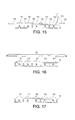
- FIGS. 12-17 illustrate a series of step used to fabricate a piezoelectric printhead utilizing a stencil to apply a paste according to an exemplary embodiment of this disclosure.
- the word “printer” encompasses any apparatus that performs a print outputting function for any purpose, such as a digital copier, bookmaking machine, facsimile machine, a multi-function machine, electrostatographic device, etc.
- a relatively thin-film piezo driver system that retains the use of existing low-cost adhesive based jet stack fabrication processes with polymers and metal foil layers.
- This approach avoids the cost and complexity of a MEMS based fabrication process.
- the piezoelectric material is deposited and built up directly on a foil using methods such as spin on or even spray solution techniques. These solutions can include a variety of Sol Gel chemistries, often built up layer by layer. This is in contrast to a traditional thick film technique where paste-like films are placed on a substrate via screen or stencil printed and fired as one layer.
- a thick film piezo driver system where a paste-like film is applied to a metal foil layer substrate which functions as a diaphragm.
- the foil which acts as a diaphragm can also act as a common electrode, often ground, while the top signal electrode can be formed by a wide variety of methods, including, but not limited to, sputtered and plated metal films, printed conductive electrodes, and blanket films, patterned or directly written.
- the foil layer substrate with the piezo material is bonded to the remainder of the jetstack as part of a final lamination process.
- addressing individual elements is accomplished by a number of means including blanket metal scribed or etched to singulate actuators, or the metal can be patterned to form electrodes directly.
- Extensions of the disclosed method and device to integrate a piezo material into a foil substrate, for use as a printhead include 1) continuous processing, where coils or webs of diaphragm stock are coated with piezo material and processed in a reel to reel fashion; 2) near net shape where punched or etched diaphragms are formed singly or in sheets and have piezo material processed directly onto them.
- an exemplary embodiment of the present disclosure including a structure for forming an actuator array driver system directly on a substrate, a diaphragm, or, specifically, a printhead structure.
- a piezo printhead array structure 8 the structure including ink chambers 76 enclosed with walls 70 , aperture plate 72 and a foil substrate 12 which functions as a diaphragm to expel ink from nozzles 74 .
- Each individual actuators 60 is attached to the foil substrate 12 and includes a top plate 50 , a first sol-gel layer 10 and a second sol-gel layer 30 .
- a voltage is applied between the top plate 50 acting as an electrode and foil substrate 12 acting as a common electrode for the printhead actuators 60 , which energizes the sol-gel layers 10 and 30 , i.e., piezoelectric material, to expand the foil substrate, i.e., diaphragm, to expel ink droplets from nozzles 74 .
- the sol-gel layers 10 and 30 i.e., piezoelectric material
- FIGS. 2-7 are cross sections depicting various in-process structures that can be formed during an embodiment of the present teachings. It will be understood that the FIGS. are generalized schematic depictions and that a structure in accordance with an embodiment may include other substructures that are not depicted for simplicity, while various depicted substructures may be removed or modified.
- FIG. 2 illustrates the deposition of a liquid actuator material 10 onto a substrate 12 from a dispenser 14 .
- the dispenser 14 may be a spin coat apparatus that includes, for example, a chuck or platform 16 that positions the substrate 12 and rotates the substrate 12 .
- Other dispensers are also contemplated including, but not limited to, a spray coating apparatus and a dip coating apparatus.
- the substrate 12 may be a printhead diaphragm that will be subsequently attached to a printhead jet stack as described below.
- the diaphragm may be removably attached to a supporting substrate during formation of the piezoelectric layer.
- the diaphragm may already be attached to a portion of the printhead jet stack such that the substrate 12 includes the printhead diaphragm and jet stack, and FIG. 2 depicts depositing the actuator material 10 onto a printhead diaphragm that is attached to a printhead jet stack.
- the substrate 12 may be a transfer layer that is not present in the final printhead structure.
- the material foil diaphragm 12 thickness is from 500 nm (0.5 ⁇ m) and 30,000 nm (30 ⁇ m).
- the actuator material 10 may be a liquid, chemically stable sol-gel solution or composite that includes a piezoelectric material in an appropriate solution.
- the sol-gel solution can include from about 0.3 moles per liter (mol/L) to about 0.7 mol/L of the piezoelectric material, wherein the piezoelectric material includes a Bi—Na—K—Ti—O oxide (i.e., an oxide that may be of the composition Bi v Na w K x Ti y O z , where the values of v-z are as described below, or another form).
- the prescribed elements are present as solubilized molecular precursors.
- the piezoelectric material may further include a Bi—Mg—Ti—O oxide (i.e., an oxide that may be in the form in the form Bi a Mg b Ti c O d , where the values of a-d are as described below, or another form).
- a Bi—Mg—Ti—O oxide i.e., an oxide that may be in the form in the form Bi a Mg b Ti c O d , where the values of a-d are as described below, or another form).
- the sol-gel solution can include the piezoelectric material, either Bi—Na—K—Ti—O or a mixture of Bi—Na—K—Ti—O and Bi—Mg—Ti—O (i.e., Bi—Na—K—Ti-O+Bi-Mg—Ti—O) in a range of from about 15 wt % to about 40 wt % of the piezoelectric sol-gel solution.
- the molecular precursors of the piezoelectric material solute are mixed with a sufficient amount of solvent and, optionally, any additional materials as described herein, such that the piezoelectric material has a concentration of from about 0.3 mol/L to about 0.7 mol/L.
- the solvent may include one or more of butanol (i.e., butyl alcohol, C 4 H 9 OH), ethanol (i.e., ethyl alcohol, C 2 H 5 OH), methanol (i.e., methyl alcohol, CH 3 OH), isopropanol (i.e., isopropyl alcohol, C 3 H 7 OH) and 2-methoxyethanol (i.e., methyl cellulose, C 3 H 8 O 2 ).
- Other alcoholic solvents are contemplated.
- the sol-gel solution may have a viscosity in the range of from about 4.0 centipoise (cP) to about 8.0 cP.
- the sol-gel solution may be prepared using various techniques.
- Bi, Na, K, and Ti precursors may be mixed within the solvent and then reacted together to form the sol-gel.
- the oxygen component to form the Bi v Na w K x Ti y O z oxide piezoelectric material is provided by the molecular precursors.
- the sol-gel is to also include Bi a Mg b Ti c O d , then Bi, Mg, and Ti precursors may be subsequently mixed in the Bi—N—K—Ti—O solution, forming a Bi v Na w K x Ti y O z —Bi a Mg b Ti c O d solid solution during the subsequent annealing process described below.
- the oxygen component to form the Bi a Mg b Ti c O d oxide piezoelectric material is provided by the molecular precursors.
- two separate solutions can be prepared.
- Bi, Na, K, and Ti precursors may be mixed within a solvent and then reacted together to form a first sol-gel component.
- Bi, Mg, and Ti precursors may be mixed within a solvent and the reacted together to form a second sol-gel component. Subsequently, the first sol-gel component and the second sol-gel component are mixed together to form the sol-gel.
- the sol-gel solution may be dispensed at a temperature of from about room temperature (i.e., about 20° C.) to about 100° C.
- the substrate 12 can be rotated by the spin coat apparatus 14 to form a thin sol-gel layer 10 having a relatively uniform thickness as depicted in FIG. 3 .
- the substrate 12 may be rotated at a speed of from about 2500 rotations per minute (rpm) to about 3500 rpm, or from about 2750 rpm to about 3250 rpm, or about 3000 rpm.
- Rotation can be performed for a duration sufficient to thin the sol-gel layer 10 to a thickness of between about 50 nanometers (nm) for each coating layer and about 200 nm for each coating layer. Multiple coating layers may be applied as described below to form a final structure having a desired thickness.
- the sol-gel layer 10 is subjected to a first curing process to partially or completely dry the sol-gel layer to remove at least part of the solvent component.
- the first curing process, and subsequent curing processes as described below, may include a drying process that heats the sol-gel layer using one or more of a sintering process, a pyrolizing process, a calcination process, and/or an annealing process.
- the molecular precursors react during this high temperature processing to result in the final oxide piezoelectric of the desired composition.
- the sol-gel layer 10 of FIG. 3 can be heated to a first temperature of from about 400° C. to about 500° C., or from about 425° C. to about 475° C., or to about 450° C.
- the first temperature can be maintained for from about 4 minutes to about 10 minutes, or from about 6 minutes to about 8 minutes, for example about 7 minutes.
- the sol-gel layer 10 can be heated to a second temperature of from about 600° C. to about 700° C., or from about 625° C. to about 675° C., or to about 650° C.
- the second temperature can be maintained for between about 1 minute and about 5 minutes, or from about 2 minutes to about 4 minutes, for example about 3 minutes.
- FIG. 4 depicts two sol-gel layers 10 , 30 that together form an actuator layer laminate or composite 32 (hereinafter, a piezoelectric composite 32 ), it will be understood that any number of actuator layers can be formed during fabrication of the piezoelectric composite 32 .
- each sol-gel layer is formed directly on the previous partially or completely cured sol-gel layer with no intervening layers between, such that the piezoelectric composite includes at least two layers of piezoelectric material that physically contact each other.
- a single actuator layer 10 may be of a sufficient thickness that additional piezoelectric layers are not needed, in which case the piezoelectric composite refers to a single piezoelectric layer.
- the FIG. 4 structure is subjected to a second or final curing process to remove most or all of the solvent component of the sol-gel layers that form the piezoelectric composite 32 .
- the final curing process can including heating the FIG. 4 structure to a temperature of from about 600° C. to about 700° C., or from about 625° C. to about 675° C., or to about 650° C. This temperature can be maintained for a duration of between about 20 minutes and about 40 minutes, or from about 25 minutes to about 35 minutes, for example about 30 minutes.
- the resulting piezoelectric composite 32 can have a desired thickness, for example from 500 nm (0.5 ⁇ m) to about 25,000 nm (0.25 ⁇ m) or from about 500 nm (0.5 ⁇ m) to about 900 nm (0.9 ⁇ m), or from about 600 nm (0.6 ⁇ m) to about 800 nm (0.8 ⁇ m), or about 700 nm (0.7 ⁇ m).
- the chemical composition of the fully cured piezoelectric composite may include Bi—Na—K—Ti—O, in the form Bi v Na w K x Ti y O z , where “v” ranges from 0 to 0.5 (i.e., 0 ⁇ 0.5, where the range of the Bi component is from 0 to 0.5 mol), “w” is in the range of about 0.5 ⁇ 1, “x” is in the range of about 0 ⁇ 0.5, “y” is in the range of about 0.5 ⁇ 1 and “z” is in the range of about 1.5 ⁇ 3.5.
- the Bi—Na—K—Ti—O may be modified with (i.e., mixed in solution with) Bi—Mg—Ti—O in the form Bi a Mg b Ti c O d , where “a” is in the range of from about 0.5 ⁇ 1, “b” is in the range of from about 0 ⁇ 0.5, “c” is in the range of from about 0 ⁇ 0.5, and “d” is in the range of from about 1.5 ⁇ 3.5.
- An embodiment can include 1 ⁇ y[Bi 0.5 (Na x , K 1-x )TiO 3 ]+yBi(Mg 0.5 ,Ti 0.5 )O 3 .
- “x” may be in the range of from about 0.5 ⁇ 0.8 and “y” may range from about 0 ⁇ 0.1.
- the piezoelectric material oxides may be in the form 0.965Bi 0.5 (Na 0.78 K 0.22 ) 0.5 TiO 3 +0.035Bi(Mg 0.5 Ti 0.5 )O 3 solid solution.
- an electrically conductive top electrode layer 40 can be formed on the exposed surface of the piezoelectric composite 32 .
- the top electrode layer 40 may be formed as a blanket layer as depicted.
- the top electrode layer 40 can be, for example, a metal such as copper, gold, titanium, nickel, or a metal alloy, or an electrically conductive non-metal, and may be formed to a thickness of from about 100 nm (0.1 ⁇ m) to about 1100 nm (1.1 ⁇ m).
- the top electrode layer 40 may be formed using sputtering, chemical vapor deposition, electroplating, or another suitable process.
- the top electrode layer 40 is patterned to result in the array of individual top electrodes (i.e., top plates) 50 as depicted in FIG. 6 .
- Patterning can be performed, for example, using a lithographic process that masks and chemically and/or mechanically etches a portion of the top electrode layer 40 to result in the top electrode array 50 .
- a laser ablation process may be used.
- the plurality of top electrodes 50 can be directly formed, written, or printed onto the top of the FIG. 4 structure such that the individual patterning of blanket layer 40 of FIG. 5 is not necessary and processing bypasses the FIG. 5 structure and proceeds directly from FIG. 4 to FIG. 5 .
- the piezoelectric composite 32 is patterned as depicted in FIG. 7 to provide an array of individual actuators 60 .
- the piezoelectric composite 32 can be patterned using, for example, lithography and chemical and/or mechanical etching, a dicing process using, for example, a dicing saw such as a wafer saw, or another process.
- the substrate 12 may be used as an etch stop layer.
- the substrate 12 in this embodiment the printhead diaphragm 12 , is removed from the platform 16 ( FIG. 2 ) if it has not already removed during prior processing.
- the printhead diaphragm 12 , array of actuators 60 , and array of top plates 50 are then bonded to a printhead jet stack using a suitable adhesive or other bonding technique, such as brazing, soldering, clamping, etc., as part of a final lamination process, ideally at a temperature to prevent damage to the material.
- the printhead jet stack may include a plurality of walls 70 and an aperture plate 72 having a plurality of nozzles 74 as depicted in FIG. 8 .
- the walls 70 , aperture plate 72 , and diaphragm 12 may provide a plurality of ink chambers 76 .
- a plurality of ink ejectors are formed in part by a nozzle 74 , an ink chamber 76 , the diaphragm 12 , an actuator 60 , and a top electrode 50 .
- Each top electrode is individually addressable through drive electronics (not individually depicted for simplicity) in electrical communication with the top electrode 50 , the diaphragm 12 , and the actuator 60 .
- the electrically conductive diaphragm 12 functions as a bottom electrode (i.e., bottom plate) that is common to a plurality of ejectors.
- ink 106 FIG.
- the associated actuator 60 bends or deflects, which deflects the diaphragm 60 over the associated ink chamber 76 , and creates a pressure pulse in the ink chamber 76 to eject ink from the associated nozzle 74 .
- the preparation for BNKT-BMT thick hybrid films can be divided into two major steps: (1) the deposition of BNKT-BMT paste using a conventional screen printing method, or other method of applying paste such as syringe dispensing, material jetting, etc., on a stainless steel membrane substrate and subsequent drying at 250° C.-600° C. for 15 minutes to 1 hour, and (2) the infiltration of the BNKT-BMT solution having the same composition of the screen printed films or other lead-free piezoelectric solution, and drying in the range of 250° C.-600° C. for 5-20 minutes. After completion of infiltration and drying process, the hybrid films are finally annealed at 650°-800° C. for 30 minutes to 2 hours. The final field thickness of the hybrid and the screen printed films is in the range of 5-50 ⁇ m.
- FIGS. 12-17 shown is a series of steps associated with producing a printhead structure using a piezo paste material according to an exemplary embodiment of this disclosure.
- a stenciling process is used to apply the piezo paste; however, it is to be understood that the exemplary embodiment provided is not limited to a stenciling process, but can also include any other method of applying paste material.
- a stencil 110 is provided which is brought into contact with a metal film substrate 12 as shown in FIG. 13 .
- a piezo paste material 112 is deposited on the stencil 110 and squeezed across the stencil 110 as shown in FIG. 15 , where the piezo paste material 112 is deposited on the foil substrate 12 .
- the stencil 110 is removed and the piezo paste is cured as shown in FIG. 17 .
- a release layer 80 may be formed over a substrate 82 , and a top electrode layer 84 may be formed on the release layer 80 .
- a piezoelectric composite 86 including one or more individual piezoelectric layers, may be formed on the top electrode layer 84 , for example, using a process as described above.
- the top electrode layer 84 and the piezoelectric composite 86 may be released from the substrate 82 , for example, by dissolving a dissolvable release layer 80 in a solvent, or by heating and flowing the release layer 80 if the release layer 80 is a thermoplastic.
- the piezoelectric composite 86 may then be bonded to a diaphragm 12 using, for example, an adhesive 90 or other bonding technique.
- the diaphragm 12 may be part of a completed jet stack 92 during attachment of the top electrode layer 84 and the piezoelectric composite 86 .
- the diaphragm 12 , top electrode layer 84 , and piezoelectric composite 86 may be subsequently attached to the jet stack 92 . In either case, processing can continue to form individual top electrodes 50 and actuators 60 , for example depicted in FIG. 8 , and other drive electronics.
- the exposed surface of the diaphragm 12 of FIG. 2 can be treated or cleaned to enhance the contact bond between the diaphragm 12 and the cured piezoelectric sol-gel solution 10 .
- the exposed surface of the diaphragm 12 can be chemically treated using, for example, one or more solvents, detergents, or a mild etchant.
- the exposed surface of the diaphragm 12 can be treated through exposure to plasma such as an oxygen plasma and/or reducing gases including hydrogen.
- the exposed surface of the diaphragm 12 can be treated using an ultrasonic cleaning process, or treated using a polishing process such as a chemical, a mechanical, or a chemical-mechanical polishing process.
- an optional adhesion layer, a buffer layer, or a surface energy modification layer can be formed over the exposed surface of the diaphragm 12 prior to applying or dispensing the sol-gel layer 10 to the diaphragm 12 .
- One or more of these treatments which may be represented by layer 80 in FIG. 9 , for example, can be performed either before or after attachment to the chuck 16 of the spin coating apparatus 14 .
- various printhead structures may be positioned in a stack press to enhance or facilitate physical and/or electrical attachment of various printhead layers.
- the completed printhead may include other ink chambers, ink paths, ink reservoirs, electrical structures that serve as drive electronics, or other electrical or mechanical structures related to the functionality, appearance, or attachment of the printhead.
- FIG. 11 depicts a printer 100 including a printer housing 102 into which at least one printhead 104 including an embodiment of the present teachings has been installed.
- the housing 102 may encase the printhead 104 .
- ink 106 is ejected from one or more printheads 104 .
- the printhead 104 is operated in accordance with digital instructions to create a desired image on a print medium 108 such as a paper sheet, plastic, etc.
- the printhead 104 may move back and forth relative to the print medium 108 in a scanning motion to generate the printed image swath by swath.
- the printhead 104 may be held fixed and the print medium 108 moved relative to it, creating an image as wide as the printhead 104 in a single pass.
- the printhead 104 can be narrower than, or as wide as, the print medium 108 .
- the printhead 104 can print to an intermediate surface such as a rotating drum or belt (not depicted for simplicity) for subsequent transfer to a print medium.
- the exemplary embodiment also relates to an apparatus for performing the operations discussed herein.
- This apparatus may be specially constructed for the required purposes, or it may comprise a general-purpose computer selectively activated or reconfigured by a computer program stored in the computer.
- a computer program may be stored in a computer readable storage medium, such as, but is not limited to, any type of disk including floppy disks, optical disks, CD-ROMs, and magnetic-optical disks, read-only memories (ROMs), random access memories (RAMs), EPROMs, EEPROMs, magnetic or optical cards, or any type of media suitable for storing electronic instructions, and each coupled to a computer system bus.
- a machine-readable medium includes any mechanism for storing or transmitting information in a form readable by a machine (e.g., a computer).
- a machine-readable medium includes read only memory (“ROM”); random access memory (“RAM”); magnetic disk storage media; optical storage media; flash memory devices; and electrical, optical, acoustical or other form of propagated signals (e.g., carrier waves, infrared signals, digital signals, etc.), just to mention a few examples.
- the methods illustrated throughout the specification may be implemented in a computer program product that may be executed on a computer.
- the computer program product may comprise a non-transitory computer-readable recording medium on which a control program is recorded, such as a disk, hard drive, or the like.
- a non-transitory computer-readable recording medium such as a disk, hard drive, or the like.
- Common forms of non-transitory computer-readable media include, for example, floppy disks, flexible disks, hard disks, magnetic tape, or any other magnetic storage medium, CD-ROM, DVD, or any other optical medium, a RAM, a PROM, an EPROM, a FLASH-EPROM, or other memory chip or cartridge, or any other tangible medium from which a computer can read and use.
- the method may be implemented in transitory media, such as a transmittable carrier wave in which the control program is embodied as a data signal using transmission media, such as acoustic or light waves, such as those generated during radio wave and infrared data communications, and the like.
- transitory media such as a transmittable carrier wave
- the control program is embodied as a data signal using transmission media, such as acoustic or light waves, such as those generated during radio wave and infrared data communications, and the like.
Landscapes
- Engineering & Computer Science (AREA)
- Manufacturing & Machinery (AREA)
- Physics & Mathematics (AREA)
- Optics & Photonics (AREA)
- Chemical & Material Sciences (AREA)
- Dispersion Chemistry (AREA)
- Particle Formation And Scattering Control In Inkjet Printers (AREA)
Abstract
Description
Claims (20)
Priority Applications (2)
| Application Number | Priority Date | Filing Date | Title |
|---|---|---|---|
| CN201710245942.XA CN107336524B (en) | 2015-09-11 | 2017-04-14 | Integrated piezoelectric printhead |
| EP17166856.9A EP3246166B1 (en) | 2015-09-11 | 2017-04-18 | Integrated piezo printhead |
Applications Claiming Priority (1)
| Application Number | Priority Date | Filing Date | Title |
|---|---|---|---|
| US14/851,422 US9662880B2 (en) | 2015-09-11 | 2015-09-11 | Integrated thin film piezoelectric printhead |
Publications (1)
| Publication Number | Publication Date |
|---|---|
| US9738070B1 true US9738070B1 (en) | 2017-08-22 |
Family
ID=58256962
Family Applications (2)
| Application Number | Title | Priority Date | Filing Date |
|---|---|---|---|
| US14/851,422 Active US9662880B2 (en) | 2015-09-11 | 2015-09-11 | Integrated thin film piezoelectric printhead |
| US15/141,229 Active US9738070B1 (en) | 2015-09-11 | 2016-04-28 | Integrated piezo printhead |
Family Applications Before (1)
| Application Number | Title | Priority Date | Filing Date |
|---|---|---|---|
| US14/851,422 Active US9662880B2 (en) | 2015-09-11 | 2015-09-11 | Integrated thin film piezoelectric printhead |
Country Status (3)
| Country | Link |
|---|---|
| US (2) | US9662880B2 (en) |
| EP (1) | EP3246166B1 (en) |
| CN (1) | CN107336524B (en) |
Cited By (1)
| Publication number | Priority date | Publication date | Assignee | Title |
|---|---|---|---|---|
| CN107336524A (en) * | 2015-09-11 | 2017-11-10 | 施乐公司 | Integrated form piezoelectric printhead |
Families Citing this family (6)
| Publication number | Priority date | Publication date | Assignee | Title |
|---|---|---|---|---|
| GB2566309B (en) | 2017-09-08 | 2021-06-16 | Xaar Technology Ltd | A method for the manufacture of a MEMS device |
| US12225822B2 (en) * | 2017-11-30 | 2025-02-11 | Jabil Inc. | System for manufacturing piezoelectronics |
| CN110642219A (en) * | 2019-09-18 | 2020-01-03 | 西安交通大学 | A beam film type PZT thin film piezoelectric array print head and its manufacturing method |
| CN111703207B (en) * | 2020-05-13 | 2021-09-14 | 苏州锐发打印技术有限公司 | Piezoelectric ink-jet printing device with single-layer internal electrode |
| US11832520B2 (en) * | 2021-04-27 | 2023-11-28 | Taiwan Semiconductor Manufacturing Company, Ltd. | Voltage breakdown uniformity in piezoelectric structure for piezoelectric devices |
| US12414474B2 (en) * | 2021-10-21 | 2025-09-09 | Baker Hughes Oilfield Operations Llc | Methods of forming piezoelectric materials, piezoelectric devices, and associated tooling and systems |
Citations (19)
| Publication number | Priority date | Publication date | Assignee | Title |
|---|---|---|---|---|
| US6158847A (en) * | 1995-07-14 | 2000-12-12 | Seiko Epson Corporation | Laminated ink-jet recording head, a process for production thereof and a printer equipped with the recording head |
| US6514427B2 (en) | 1999-10-18 | 2003-02-04 | Matsushita Electric Industrial Co., Ltd. | Piezoelectric ceramic composition and piezoelectric element containing the same |
| US20040164650A1 (en) * | 2003-02-25 | 2004-08-26 | Palo Alto Research Center Incorporated | Methods to make piezoelectric ceramic thick film array and single elements and devices |
| US6955419B2 (en) | 2003-11-05 | 2005-10-18 | Xerox Corporation | Ink jet apparatus |
| US6987348B2 (en) | 2002-12-13 | 2006-01-17 | Palo Alto Research Center Inc. | Piezoelectric transducers |
| US7048361B2 (en) | 2003-11-05 | 2006-05-23 | Xerox Corporation | Ink jet apparatus |
| US20070008388A1 (en) | 2004-03-02 | 2007-01-11 | Kiyoshi Yamaguchi | Liquid drop discharge head, liquid drop discharge device, and image forming device |
| US7965021B2 (en) | 2009-01-20 | 2011-06-21 | Panasonic Corporation | Piezoelectric thin film and method of manufacturing the same, ink jet head, method of forming image with the ink jet head, angular velocity sensor, method of measuring angular velocity with the angular velocity sensor, piezoelectric generating element, and method of generating electric power with the piezoelectric generating element |
| WO2011129072A1 (en) | 2010-04-15 | 2011-10-20 | パナソニック株式会社 | Piezoelectric thin film, ink-jet head, method for forming image using ink-jet head, angular-velocity sensor, method for determining angular velocity using angular-velocity sensor, piezoelectric power-generating element, and method for generating power using piezoelectric power-generating element |
| WO2011158491A1 (en) | 2010-06-16 | 2011-12-22 | パナソニック株式会社 | Piezoelectric membrane, inkjet head, method using an inkjet head to form images, angular-velocity sensor, method using an angular-velocity sensor to measure angular velocity, piezoelectric generation element, and electricity-generation method using piezoelectric generation elements |
| US8183748B2 (en) | 2009-10-13 | 2012-05-22 | Panasonic Corporation | Piezoelectric thin film, ink jet head, method for forming image with the ink jet head, angular velocity sensor, method for measuring angular velocity with the angular velocity sensor, piezoelectric generating element and method for generating electric power with the piezoelectric generating element |
| WO2012104945A1 (en) | 2011-02-03 | 2012-08-09 | パナソニック株式会社 | Piezoelectric thin film, method for manufacturing same, inkjet head, method for forming image using inkjet head, angular velocity sensor, method for measuring angular velocity using angular velocity sensor, piezoelectric power generation element, and method for generating power using piezoelectric power generation element |
| US8288020B2 (en) | 2009-04-20 | 2012-10-16 | Panasonic Corporation | Piezoelectric thin film and method of manufacturing the same, ink jet head, method of forming image with the ink jet head, angular velocity sensor, method of measuring angular velocity with the angular velocity sensor, piezoelectric generating element, and method of generating electric power with the piezoelectric generating element |
| US8390179B2 (en) | 2010-06-16 | 2013-03-05 | Panasonic Corporation | Piezoelectric film and method of manufacturing the same, ink jet head, method of forming image by the ink jet head, angular velocity sensor, method of measuring angular velocity by the angular velocity sensor, piezoelectric generating element, and method of generating electric power using the piezoelectric generating element |
| US8393719B2 (en) | 2010-06-16 | 2013-03-12 | Panasonic Corporation | Piezoelectric film, ink jet head, method of forming image by the ink jet head, angular velocity sensor, method of measuring angular velocity by the angular velocity sensor, piezoelectric generating element, and method of generating electric power using the piezoelectric generating element |
| US20130155155A1 (en) | 2011-12-20 | 2013-06-20 | Seiko Epson Corporation | Liquid ejecting head, liquid ejecting apparatus, and piezoelectric element |
| US20130162708A1 (en) | 2011-12-26 | 2013-06-27 | Seiko Epson Corporation | Liquid ejecting apparatus and control method of liquid ejecting head |
| US20130169716A1 (en) | 2011-12-28 | 2013-07-04 | Seiko Epson Corporation | Liquid ejecting apparatus |
| US20130222482A1 (en) | 2012-02-28 | 2013-08-29 | Canon Kabushiki Kaisha | Piezoelectric element, liquid discharge head and liquid discharge apparatus |
Family Cites Families (8)
| Publication number | Priority date | Publication date | Assignee | Title |
|---|---|---|---|---|
| JPH10202874A (en) * | 1997-01-24 | 1998-08-04 | Seiko Epson Corp | Ink jet printer head and method of manufacturing the same |
| JP3666177B2 (en) * | 1997-04-14 | 2005-06-29 | 松下電器産業株式会社 | Inkjet recording device |
| US7175262B2 (en) * | 2002-03-18 | 2007-02-13 | Seiko Epson Corporation | Liquid-jet head, method of manufacturing the same and liquid-jet apparatus |
| JP3952048B2 (en) * | 2003-09-29 | 2007-08-01 | ブラザー工業株式会社 | Liquid transfer device and method for manufacturing liquid transfer device |
| JP4218594B2 (en) * | 2004-06-08 | 2009-02-04 | ブラザー工業株式会社 | Inkjet head |
| JP5476901B2 (en) * | 2009-09-30 | 2014-04-23 | ブラザー工業株式会社 | Method for manufacturing piezoelectric actuator and piezoelectric actuator |
| JP6011760B2 (en) * | 2011-12-08 | 2016-10-19 | セイコーエプソン株式会社 | Piezoelectric element manufacturing method, liquid ejecting head manufacturing method, and liquid ejecting apparatus manufacturing method |
| US9662880B2 (en) * | 2015-09-11 | 2017-05-30 | Xerox Corporation | Integrated thin film piezoelectric printhead |
-
2015
- 2015-09-11 US US14/851,422 patent/US9662880B2/en active Active
-
2016
- 2016-04-28 US US15/141,229 patent/US9738070B1/en active Active
-
2017
- 2017-04-14 CN CN201710245942.XA patent/CN107336524B/en active Active
- 2017-04-18 EP EP17166856.9A patent/EP3246166B1/en active Active
Patent Citations (22)
| Publication number | Priority date | Publication date | Assignee | Title |
|---|---|---|---|---|
| US6158847A (en) * | 1995-07-14 | 2000-12-12 | Seiko Epson Corporation | Laminated ink-jet recording head, a process for production thereof and a printer equipped with the recording head |
| US6514427B2 (en) | 1999-10-18 | 2003-02-04 | Matsushita Electric Industrial Co., Ltd. | Piezoelectric ceramic composition and piezoelectric element containing the same |
| US6987348B2 (en) | 2002-12-13 | 2006-01-17 | Palo Alto Research Center Inc. | Piezoelectric transducers |
| US20040164650A1 (en) * | 2003-02-25 | 2004-08-26 | Palo Alto Research Center Incorporated | Methods to make piezoelectric ceramic thick film array and single elements and devices |
| US6955419B2 (en) | 2003-11-05 | 2005-10-18 | Xerox Corporation | Ink jet apparatus |
| US7048361B2 (en) | 2003-11-05 | 2006-05-23 | Xerox Corporation | Ink jet apparatus |
| US20070008388A1 (en) | 2004-03-02 | 2007-01-11 | Kiyoshi Yamaguchi | Liquid drop discharge head, liquid drop discharge device, and image forming device |
| US7965021B2 (en) | 2009-01-20 | 2011-06-21 | Panasonic Corporation | Piezoelectric thin film and method of manufacturing the same, ink jet head, method of forming image with the ink jet head, angular velocity sensor, method of measuring angular velocity with the angular velocity sensor, piezoelectric generating element, and method of generating electric power with the piezoelectric generating element |
| US8288020B2 (en) | 2009-04-20 | 2012-10-16 | Panasonic Corporation | Piezoelectric thin film and method of manufacturing the same, ink jet head, method of forming image with the ink jet head, angular velocity sensor, method of measuring angular velocity with the angular velocity sensor, piezoelectric generating element, and method of generating electric power with the piezoelectric generating element |
| US8183748B2 (en) | 2009-10-13 | 2012-05-22 | Panasonic Corporation | Piezoelectric thin film, ink jet head, method for forming image with the ink jet head, angular velocity sensor, method for measuring angular velocity with the angular velocity sensor, piezoelectric generating element and method for generating electric power with the piezoelectric generating element |
| US20120038714A1 (en) | 2010-04-15 | 2012-02-16 | Panasonic Corporation | Piezoelectric thin film, ink jet head, method of forming image by the ink jet head, angular velocity sensor, method of measuring angular velocity by the angular velocity sensor, piezoelectric generating element, and method of generating electric power using the piezoelectric generating element |
| WO2011129072A1 (en) | 2010-04-15 | 2011-10-20 | パナソニック株式会社 | Piezoelectric thin film, ink-jet head, method for forming image using ink-jet head, angular-velocity sensor, method for determining angular velocity using angular-velocity sensor, piezoelectric power-generating element, and method for generating power using piezoelectric power-generating element |
| WO2011158491A1 (en) | 2010-06-16 | 2011-12-22 | パナソニック株式会社 | Piezoelectric membrane, inkjet head, method using an inkjet head to form images, angular-velocity sensor, method using an angular-velocity sensor to measure angular velocity, piezoelectric generation element, and electricity-generation method using piezoelectric generation elements |
| US20120281046A1 (en) | 2010-06-16 | 2012-11-08 | Panasonic Corporation | Piezoelectric film and method of manufacturing the same, ink jet head, method of forming image by the ink jet head, angular velocity sensor, method of measuring angular velocity by the angular velocity sensor, piezoelectric generating element, and method of generating electric power using the piezoelectric generating element |
| US8390179B2 (en) | 2010-06-16 | 2013-03-05 | Panasonic Corporation | Piezoelectric film and method of manufacturing the same, ink jet head, method of forming image by the ink jet head, angular velocity sensor, method of measuring angular velocity by the angular velocity sensor, piezoelectric generating element, and method of generating electric power using the piezoelectric generating element |
| US8393719B2 (en) | 2010-06-16 | 2013-03-12 | Panasonic Corporation | Piezoelectric film, ink jet head, method of forming image by the ink jet head, angular velocity sensor, method of measuring angular velocity by the angular velocity sensor, piezoelectric generating element, and method of generating electric power using the piezoelectric generating element |
| WO2012104945A1 (en) | 2011-02-03 | 2012-08-09 | パナソニック株式会社 | Piezoelectric thin film, method for manufacturing same, inkjet head, method for forming image using inkjet head, angular velocity sensor, method for measuring angular velocity using angular velocity sensor, piezoelectric power generation element, and method for generating power using piezoelectric power generation element |
| US20130136951A1 (en) | 2011-02-03 | 2013-05-30 | Panasonic Corporation | Piezoelectric thin film, method for manufacturing same, inkjet head, method for forming image using inkjet head, angular velocity sensor, method for measuring angular velocity using angular velocity sensor, piezoelectric power generation element, and method for generating power using piezoelectric power generation element |
| US20130155155A1 (en) | 2011-12-20 | 2013-06-20 | Seiko Epson Corporation | Liquid ejecting head, liquid ejecting apparatus, and piezoelectric element |
| US20130162708A1 (en) | 2011-12-26 | 2013-06-27 | Seiko Epson Corporation | Liquid ejecting apparatus and control method of liquid ejecting head |
| US20130169716A1 (en) | 2011-12-28 | 2013-07-04 | Seiko Epson Corporation | Liquid ejecting apparatus |
| US20130222482A1 (en) | 2012-02-28 | 2013-08-29 | Canon Kabushiki Kaisha | Piezoelectric element, liquid discharge head and liquid discharge apparatus |
Non-Patent Citations (1)
| Title |
|---|
| U.S. Appl. No. 14/851,422, filed Sep. 11, 2015, Hays et al. |
Cited By (2)
| Publication number | Priority date | Publication date | Assignee | Title |
|---|---|---|---|---|
| CN107336524A (en) * | 2015-09-11 | 2017-11-10 | 施乐公司 | Integrated form piezoelectric printhead |
| CN107336524B (en) * | 2015-09-11 | 2020-05-22 | 施乐公司 | Integrated piezoelectric printhead |
Also Published As
| Publication number | Publication date |
|---|---|
| US9662880B2 (en) | 2017-05-30 |
| US20170072691A1 (en) | 2017-03-16 |
| EP3246166A3 (en) | 2018-03-07 |
| CN107336524B (en) | 2020-05-22 |
| EP3246166B1 (en) | 2021-08-25 |
| EP3246166A2 (en) | 2017-11-22 |
| CN107336524A (en) | 2017-11-10 |
Similar Documents
| Publication | Publication Date | Title |
|---|---|---|
| US9738070B1 (en) | Integrated piezo printhead | |
| US8425026B2 (en) | Electromechanical transducer film and method for manufacturing electromechanical transducer film | |
| US9085145B2 (en) | Method of forming electromechanical transducer film, electromechanical transducer film, electromechanical transducer element, and liquid discharge head | |
| WO2010137737A1 (en) | Method for producing electromechanical transducer, electromechanical transducer produced by the method, liquid-droplet jetting head, and liquid-droplet jetting apparatus | |
| JP6680301B2 (en) | INKJET HEAD, METHOD FOR MANUFACTURING THE SAME, AND INKJET RECORDING DEVICE | |
| JP2017112281A (en) | Electromechanical conversion element, liquid discharge head, liquid discharging device, method for manufacturing electromechanical conversion film, and method for manufacturing liquid discharge head | |
| JP6442860B2 (en) | Precursor sol-gel solution, electromechanical transducer, droplet discharge head, and ink jet recording apparatus | |
| JP5884272B2 (en) | Thin film manufacturing method | |
| JP2016062984A (en) | Piezoelectric actuator, manufacturing method thereof, liquid cartridge, and image forming apparatus | |
| JP6281629B2 (en) | Substrate with piezoelectric thin film, piezoelectric actuator, ink jet head, ink jet printer, and method for manufacturing ferroelectric thin film | |
| JP6390177B2 (en) | Method for producing electro-mechanical conversion film | |
| JP2016155283A (en) | Electromechanical conversion member, droplet discharge head, image forming apparatus, ink cartridge, micropump, and electromechanical conversion member manufacturing method | |
| JP6606933B2 (en) | Substrate manufacturing method and droplet discharge head manufacturing method | |
| JP6287188B2 (en) | Piezoelectric actuator, method for manufacturing piezoelectric actuator, droplet discharge head, liquid cartridge, and image forming apparatus | |
| JP5754198B2 (en) | Liquid ejecting head, liquid ejecting apparatus, and piezoelectric actuator | |
| JP5853355B2 (en) | Electric-mechanical conversion membrane manufacturing method | |
| JP2001047623A (en) | Inkjet printer head | |
| JP2005246789A (en) | Liquid discharge head and its manufacturing method | |
| JP2013045783A (en) | Thin film manufacturing device and thin film manufacturing method | |
| JP2013146657A (en) | Method for producing film pattern, electromechanical conversion film, electromechanical transducer, liquid discharge head, and image forming apparatus | |
| JP2012186278A (en) | Manufacturing method of electromechanical conversion film and electromechanical conversion film | |
| JP2013065698A (en) | Electro-mechanical conversion element, droplet discharge head, droplet discharge device, and image forming apparatus | |
| JP2010214801A (en) | Liquid jetting head, liquid jetting apparatus and piezoelectric element | |
| JP2005353746A (en) | Actuator and inkjet head | |
| JP2008142966A (en) | Inkjet recording head |
Legal Events
| Date | Code | Title | Description |
|---|---|---|---|
| AS | Assignment |
Owner name: XEROX CORPORATION, CONNECTICUT Free format text: ASSIGNMENT OF ASSIGNORS INTEREST;ASSIGNORS:NYSTROM, PETER J.;HAYS, ANDREW W.;KINGON, ANGUS I.;AND OTHERS;SIGNING DATES FROM 20160426 TO 20160427;REEL/FRAME:038411/0315 |
|
| AS | Assignment |
Owner name: BROWN UNIVERSITY, RHODE ISLAND Free format text: ASSIGNMENT OF ASSIGNORS INTEREST;ASSIGNORS:KINGON, ANGUS I.;KIM, SEUNGHYUN;SIGNING DATES FROM 20170224 TO 20170228;REEL/FRAME:041419/0957 Owner name: XEROX CORPORATION, CONNECTICUT Free format text: CORRECTIVE ASSIGNMENT TO CORRECT THE INVENTORSHIP REMOVING ANGUS I. KINGON AND SEUNGHYUN KIM PREVIOUSLY RECORDED ON REEL 038411 FRAME 0315. ASSIGNOR(S) HEREBY CONFIRMS THE ASSIGNMENT;ASSIGNORS:HAYS, ANDREW W.;NYSTROM, PETER J.;REEL/FRAME:041840/0534 Effective date: 20160426 |
|
| STCF | Information on status: patent grant |
Free format text: PATENTED CASE |
|
| MAFP | Maintenance fee payment |
Free format text: PAYMENT OF MAINTENANCE FEE, 4TH YEAR, LARGE ENTITY (ORIGINAL EVENT CODE: M1551); ENTITY STATUS OF PATENT OWNER: LARGE ENTITY Year of fee payment: 4 |
|
| AS | Assignment |
Owner name: CITIBANK, N.A., AS COLLATERAL AGENT, NEW YORK Free format text: SECURITY INTEREST;ASSIGNOR:XEROX CORPORATION;REEL/FRAME:064760/0389 Effective date: 20230621 |
|
| AS | Assignment |
Owner name: JEFFERIES FINANCE LLC, AS COLLATERAL AGENT, NEW YORK Free format text: SECURITY INTEREST;ASSIGNOR:XEROX CORPORATION;REEL/FRAME:065628/0019 Effective date: 20231117 |
|
| AS | Assignment |
Owner name: XEROX CORPORATION, CONNECTICUT Free format text: TERMINATION AND RELEASE OF SECURITY INTEREST IN PATENTS RECORDED AT RF 064760/0389;ASSIGNOR:CITIBANK, N.A., AS COLLATERAL AGENT;REEL/FRAME:068261/0001 Effective date: 20240206 Owner name: CITIBANK, N.A., AS COLLATERAL AGENT, NEW YORK Free format text: SECURITY INTEREST;ASSIGNOR:XEROX CORPORATION;REEL/FRAME:066741/0001 Effective date: 20240206 |
|
| MAFP | Maintenance fee payment |
Free format text: PAYMENT OF MAINTENANCE FEE, 8TH YEAR, LARGE ENTITY (ORIGINAL EVENT CODE: M1552); ENTITY STATUS OF PATENT OWNER: LARGE ENTITY Year of fee payment: 8 |
|
| AS | Assignment |
Owner name: U.S. BANK TRUST COMPANY, NATIONAL ASSOCIATION, AS COLLATERAL AGENT, CONNECTICUT Free format text: FIRST LIEN NOTES PATENT SECURITY AGREEMENT;ASSIGNOR:XEROX CORPORATION;REEL/FRAME:070824/0001 Effective date: 20250411 |
|
| AS | Assignment |
Owner name: U.S. BANK TRUST COMPANY, NATIONAL ASSOCIATION, AS COLLATERAL AGENT, CONNECTICUT Free format text: SECOND LIEN NOTES PATENT SECURITY AGREEMENT;ASSIGNOR:XEROX CORPORATION;REEL/FRAME:071785/0550 Effective date: 20250701 |