US9711615B2 - Multichannel devices with improved performance and methods of making the same - Google Patents
Multichannel devices with improved performance and methods of making the same Download PDFInfo
- Publication number
- US9711615B2 US9711615B2 US15/222,039 US201615222039A US9711615B2 US 9711615 B2 US9711615 B2 US 9711615B2 US 201615222039 A US201615222039 A US 201615222039A US 9711615 B2 US9711615 B2 US 9711615B2
- Authority
- US
- United States
- Prior art keywords
- heterostructure
- channel
- layer
- heterostructures
- thickness
- Prior art date
- Legal status (The legal status is an assumption and is not a legal conclusion. Google has not performed a legal analysis and makes no representation as to the accuracy of the status listed.)
- Active
Links
- 238000000034 method Methods 0.000 title claims description 47
- 239000002019 doping agent Substances 0.000 claims description 26
- 238000000151 deposition Methods 0.000 claims description 14
- 230000008569 process Effects 0.000 claims description 14
- 238000005530 etching Methods 0.000 claims description 8
- 229910002601 GaN Inorganic materials 0.000 description 61
- JMASRVWKEDWRBT-UHFFFAOYSA-N Gallium nitride Chemical compound [Ga]#N JMASRVWKEDWRBT-UHFFFAOYSA-N 0.000 description 59
- 239000000463 material Substances 0.000 description 27
- 230000000694 effects Effects 0.000 description 19
- 230000004888 barrier function Effects 0.000 description 12
- 230000005684 electric field Effects 0.000 description 12
- 238000004519 manufacturing process Methods 0.000 description 11
- 239000000969 carrier Substances 0.000 description 10
- 230000015556 catabolic process Effects 0.000 description 6
- 230000006911 nucleation Effects 0.000 description 6
- 238000010899 nucleation Methods 0.000 description 6
- RNQKDQAVIXDKAG-UHFFFAOYSA-N aluminum gallium Chemical compound [Al].[Ga] RNQKDQAVIXDKAG-UHFFFAOYSA-N 0.000 description 5
- 230000015572 biosynthetic process Effects 0.000 description 5
- 230000008021 deposition Effects 0.000 description 5
- PXHVJJICTQNCMI-UHFFFAOYSA-N Nickel Chemical compound [Ni] PXHVJJICTQNCMI-UHFFFAOYSA-N 0.000 description 4
- 229910052782 aluminium Inorganic materials 0.000 description 4
- XAGFODPZIPBFFR-UHFFFAOYSA-N aluminium Chemical compound [Al] XAGFODPZIPBFFR-UHFFFAOYSA-N 0.000 description 4
- 239000000203 mixture Substances 0.000 description 4
- 229920002120 photoresistant polymer Polymers 0.000 description 4
- 239000007787 solid Substances 0.000 description 4
- 230000005533 two-dimensional electron gas Effects 0.000 description 4
- 239000004047 hole gas Substances 0.000 description 3
- 238000001020 plasma etching Methods 0.000 description 3
- 230000010287 polarization Effects 0.000 description 3
- 230000004044 response Effects 0.000 description 3
- 239000000758 substrate Substances 0.000 description 3
- 230000008719 thickening Effects 0.000 description 3
- 229910052581 Si3N4 Inorganic materials 0.000 description 2
- VYPSYNLAJGMNEJ-UHFFFAOYSA-N Silicium dioxide Chemical compound O=[Si]=O VYPSYNLAJGMNEJ-UHFFFAOYSA-N 0.000 description 2
- FTWRSWRBSVXQPI-UHFFFAOYSA-N alumanylidynearsane;gallanylidynearsane Chemical compound [As]#[Al].[As]#[Ga] FTWRSWRBSVXQPI-UHFFFAOYSA-N 0.000 description 2
- 230000008901 benefit Effects 0.000 description 2
- 230000007423 decrease Effects 0.000 description 2
- 230000003247 decreasing effect Effects 0.000 description 2
- 238000009826 distribution Methods 0.000 description 2
- 238000005516 engineering process Methods 0.000 description 2
- 230000005669 field effect Effects 0.000 description 2
- 239000012212 insulator Substances 0.000 description 2
- 239000011777 magnesium Substances 0.000 description 2
- 229910052751 metal Inorganic materials 0.000 description 2
- 239000002184 metal Substances 0.000 description 2
- 229910052759 nickel Inorganic materials 0.000 description 2
- 238000000059 patterning Methods 0.000 description 2
- 230000009467 reduction Effects 0.000 description 2
- HQVNEWCFYHHQES-UHFFFAOYSA-N silicon nitride Chemical compound N12[Si]34N5[Si]62N3[Si]51N64 HQVNEWCFYHHQES-UHFFFAOYSA-N 0.000 description 2
- 229910052814 silicon oxide Inorganic materials 0.000 description 2
- 230000002269 spontaneous effect Effects 0.000 description 2
- PIGFYZPCRLYGLF-UHFFFAOYSA-N Aluminum nitride Chemical compound [Al]#N PIGFYZPCRLYGLF-UHFFFAOYSA-N 0.000 description 1
- JBRZTFJDHDCESZ-UHFFFAOYSA-N AsGa Chemical compound [As]#[Ga] JBRZTFJDHDCESZ-UHFFFAOYSA-N 0.000 description 1
- OKTJSMMVPCPJKN-UHFFFAOYSA-N Carbon Chemical compound [C] OKTJSMMVPCPJKN-UHFFFAOYSA-N 0.000 description 1
- GYHNNYVSQQEPJS-UHFFFAOYSA-N Gallium Chemical compound [Ga] GYHNNYVSQQEPJS-UHFFFAOYSA-N 0.000 description 1
- FYYHWMGAXLPEAU-UHFFFAOYSA-N Magnesium Chemical compound [Mg] FYYHWMGAXLPEAU-UHFFFAOYSA-N 0.000 description 1
- 229910000676 Si alloy Inorganic materials 0.000 description 1
- XUIMIQQOPSSXEZ-UHFFFAOYSA-N Silicon Chemical compound [Si] XUIMIQQOPSSXEZ-UHFFFAOYSA-N 0.000 description 1
- 230000004075 alteration Effects 0.000 description 1
- AUCDRFABNLOFRE-UHFFFAOYSA-N alumane;indium Chemical compound [AlH3].[In] AUCDRFABNLOFRE-UHFFFAOYSA-N 0.000 description 1
- 238000000231 atomic layer deposition Methods 0.000 description 1
- 229910052799 carbon Inorganic materials 0.000 description 1
- 238000005229 chemical vapour deposition Methods 0.000 description 1
- 239000004020 conductor Substances 0.000 description 1
- PMHQVHHXPFUNSP-UHFFFAOYSA-M copper(1+);methylsulfanylmethane;bromide Chemical compound Br[Cu].CSC PMHQVHHXPFUNSP-UHFFFAOYSA-M 0.000 description 1
- 238000005336 cracking Methods 0.000 description 1
- 229910021419 crystalline silicon Inorganic materials 0.000 description 1
- 230000001419 dependent effect Effects 0.000 description 1
- 229910052731 fluorine Inorganic materials 0.000 description 1
- 239000011737 fluorine Substances 0.000 description 1
- -1 fluorine ions Chemical class 0.000 description 1
- 229910052733 gallium Inorganic materials 0.000 description 1
- 229910052732 germanium Inorganic materials 0.000 description 1
- GNPVGFCGXDBREM-UHFFFAOYSA-N germanium atom Chemical compound [Ge] GNPVGFCGXDBREM-UHFFFAOYSA-N 0.000 description 1
- PCHJSUWPFVWCPO-UHFFFAOYSA-N gold Chemical compound [Au] PCHJSUWPFVWCPO-UHFFFAOYSA-N 0.000 description 1
- 229910052737 gold Inorganic materials 0.000 description 1
- 239000010931 gold Substances 0.000 description 1
- 230000006872 improvement Effects 0.000 description 1
- 238000009616 inductively coupled plasma Methods 0.000 description 1
- 229910052749 magnesium Inorganic materials 0.000 description 1
- 230000004048 modification Effects 0.000 description 1
- 238000012986 modification Methods 0.000 description 1
- 238000001451 molecular beam epitaxy Methods 0.000 description 1
- 238000005457 optimization Methods 0.000 description 1
- 238000002161 passivation Methods 0.000 description 1
- 229910052594 sapphire Inorganic materials 0.000 description 1
- 239000010980 sapphire Substances 0.000 description 1
- 239000004065 semiconductor Substances 0.000 description 1
- 229910052710 silicon Inorganic materials 0.000 description 1
- 239000010703 silicon Substances 0.000 description 1
- HBMJWWWQQXIZIP-UHFFFAOYSA-N silicon carbide Chemical compound [Si+]#[C-] HBMJWWWQQXIZIP-UHFFFAOYSA-N 0.000 description 1
- 238000004088 simulation Methods 0.000 description 1
Images


Classifications
-
- H—ELECTRICITY
- H01—ELECTRIC ELEMENTS
- H01L—SEMICONDUCTOR DEVICES NOT COVERED BY CLASS H10
- H01L29/00—Semiconductor devices adapted for rectifying, amplifying, oscillating or switching, or capacitors or resistors with at least one potential-jump barrier or surface barrier, e.g. PN junction depletion layer or carrier concentration layer; Details of semiconductor bodies or of electrodes thereof ; Multistep manufacturing processes therefor
- H01L29/66—Types of semiconductor device ; Multistep manufacturing processes therefor
- H01L29/68—Types of semiconductor device ; Multistep manufacturing processes therefor controllable by only the electric current supplied, or only the electric potential applied, to an electrode which does not carry the current to be rectified, amplified or switched
- H01L29/76—Unipolar devices, e.g. field effect transistors
- H01L29/772—Field effect transistors
- H01L29/778—Field effect transistors with two-dimensional charge carrier gas channel, e.g. HEMT ; with two-dimensional charge-carrier layer formed at a heterojunction interface
- H01L29/7782—Field effect transistors with two-dimensional charge carrier gas channel, e.g. HEMT ; with two-dimensional charge-carrier layer formed at a heterojunction interface with confinement of carriers by at least two heterojunctions, e.g. DHHEMT, quantum well HEMT, DHMODFET
- H01L29/7783—Field effect transistors with two-dimensional charge carrier gas channel, e.g. HEMT ; with two-dimensional charge-carrier layer formed at a heterojunction interface with confinement of carriers by at least two heterojunctions, e.g. DHHEMT, quantum well HEMT, DHMODFET using III-V semiconductor material
- H01L29/7785—Field effect transistors with two-dimensional charge carrier gas channel, e.g. HEMT ; with two-dimensional charge-carrier layer formed at a heterojunction interface with confinement of carriers by at least two heterojunctions, e.g. DHHEMT, quantum well HEMT, DHMODFET using III-V semiconductor material with more than one donor layer
-
- H—ELECTRICITY
- H01—ELECTRIC ELEMENTS
- H01L—SEMICONDUCTOR DEVICES NOT COVERED BY CLASS H10
- H01L21/00—Processes or apparatus adapted for the manufacture or treatment of semiconductor or solid state devices or of parts thereof
- H01L21/02—Manufacture or treatment of semiconductor devices or of parts thereof
- H01L21/04—Manufacture or treatment of semiconductor devices or of parts thereof the devices having at least one potential-jump barrier or surface barrier, e.g. PN junction, depletion layer or carrier concentration layer
- H01L21/18—Manufacture or treatment of semiconductor devices or of parts thereof the devices having at least one potential-jump barrier or surface barrier, e.g. PN junction, depletion layer or carrier concentration layer the devices having semiconductor bodies comprising elements of Group IV of the Periodic System or AIIIBV compounds with or without impurities, e.g. doping materials
- H01L21/30—Treatment of semiconductor bodies using processes or apparatus not provided for in groups H01L21/20 - H01L21/26
- H01L21/302—Treatment of semiconductor bodies using processes or apparatus not provided for in groups H01L21/20 - H01L21/26 to change their surface-physical characteristics or shape, e.g. etching, polishing, cutting
- H01L21/306—Chemical or electrical treatment, e.g. electrolytic etching
- H01L21/3065—Plasma etching; Reactive-ion etching
-
- H—ELECTRICITY
- H01—ELECTRIC ELEMENTS
- H01L—SEMICONDUCTOR DEVICES NOT COVERED BY CLASS H10
- H01L29/00—Semiconductor devices adapted for rectifying, amplifying, oscillating or switching, or capacitors or resistors with at least one potential-jump barrier or surface barrier, e.g. PN junction depletion layer or carrier concentration layer; Details of semiconductor bodies or of electrodes thereof ; Multistep manufacturing processes therefor
- H01L29/02—Semiconductor bodies ; Multistep manufacturing processes therefor
- H01L29/06—Semiconductor bodies ; Multistep manufacturing processes therefor characterised by their shape; characterised by the shapes, relative sizes, or dispositions of the semiconductor regions ; characterised by the concentration or distribution of impurities within semiconductor regions
- H01L29/10—Semiconductor bodies ; Multistep manufacturing processes therefor characterised by their shape; characterised by the shapes, relative sizes, or dispositions of the semiconductor regions ; characterised by the concentration or distribution of impurities within semiconductor regions with semiconductor regions connected to an electrode not carrying current to be rectified, amplified or switched and such electrode being part of a semiconductor device which comprises three or more electrodes
- H01L29/1025—Channel region of field-effect devices
- H01L29/1029—Channel region of field-effect devices of field-effect transistors
- H01L29/1058—Channel region of field-effect devices of field-effect transistors with PN junction gate
-
- H—ELECTRICITY
- H01—ELECTRIC ELEMENTS
- H01L—SEMICONDUCTOR DEVICES NOT COVERED BY CLASS H10
- H01L29/00—Semiconductor devices adapted for rectifying, amplifying, oscillating or switching, or capacitors or resistors with at least one potential-jump barrier or surface barrier, e.g. PN junction depletion layer or carrier concentration layer; Details of semiconductor bodies or of electrodes thereof ; Multistep manufacturing processes therefor
- H01L29/02—Semiconductor bodies ; Multistep manufacturing processes therefor
- H01L29/12—Semiconductor bodies ; Multistep manufacturing processes therefor characterised by the materials of which they are formed
- H01L29/15—Structures with periodic or quasi periodic potential variation, e.g. multiple quantum wells, superlattices
- H01L29/157—Doping structures, e.g. doping superlattices, nipi superlattices
-
- H—ELECTRICITY
- H01—ELECTRIC ELEMENTS
- H01L—SEMICONDUCTOR DEVICES NOT COVERED BY CLASS H10
- H01L29/00—Semiconductor devices adapted for rectifying, amplifying, oscillating or switching, or capacitors or resistors with at least one potential-jump barrier or surface barrier, e.g. PN junction depletion layer or carrier concentration layer; Details of semiconductor bodies or of electrodes thereof ; Multistep manufacturing processes therefor
- H01L29/02—Semiconductor bodies ; Multistep manufacturing processes therefor
- H01L29/12—Semiconductor bodies ; Multistep manufacturing processes therefor characterised by the materials of which they are formed
- H01L29/20—Semiconductor bodies ; Multistep manufacturing processes therefor characterised by the materials of which they are formed including, apart from doping materials or other impurities, only AIIIBV compounds
- H01L29/2003—Nitride compounds
-
- H—ELECTRICITY
- H01—ELECTRIC ELEMENTS
- H01L—SEMICONDUCTOR DEVICES NOT COVERED BY CLASS H10
- H01L29/00—Semiconductor devices adapted for rectifying, amplifying, oscillating or switching, or capacitors or resistors with at least one potential-jump barrier or surface barrier, e.g. PN junction depletion layer or carrier concentration layer; Details of semiconductor bodies or of electrodes thereof ; Multistep manufacturing processes therefor
- H01L29/02—Semiconductor bodies ; Multistep manufacturing processes therefor
- H01L29/12—Semiconductor bodies ; Multistep manufacturing processes therefor characterised by the materials of which they are formed
- H01L29/20—Semiconductor bodies ; Multistep manufacturing processes therefor characterised by the materials of which they are formed including, apart from doping materials or other impurities, only AIIIBV compounds
- H01L29/201—Semiconductor bodies ; Multistep manufacturing processes therefor characterised by the materials of which they are formed including, apart from doping materials or other impurities, only AIIIBV compounds including two or more compounds, e.g. alloys
- H01L29/205—Semiconductor bodies ; Multistep manufacturing processes therefor characterised by the materials of which they are formed including, apart from doping materials or other impurities, only AIIIBV compounds including two or more compounds, e.g. alloys in different semiconductor regions, e.g. heterojunctions
-
- H—ELECTRICITY
- H01—ELECTRIC ELEMENTS
- H01L—SEMICONDUCTOR DEVICES NOT COVERED BY CLASS H10
- H01L29/00—Semiconductor devices adapted for rectifying, amplifying, oscillating or switching, or capacitors or resistors with at least one potential-jump barrier or surface barrier, e.g. PN junction depletion layer or carrier concentration layer; Details of semiconductor bodies or of electrodes thereof ; Multistep manufacturing processes therefor
- H01L29/66—Types of semiconductor device ; Multistep manufacturing processes therefor
- H01L29/66007—Multistep manufacturing processes
- H01L29/66075—Multistep manufacturing processes of devices having semiconductor bodies comprising group 14 or group 13/15 materials
- H01L29/66227—Multistep manufacturing processes of devices having semiconductor bodies comprising group 14 or group 13/15 materials the devices being controllable only by the electric current supplied or the electric potential applied, to an electrode which does not carry the current to be rectified, amplified or switched, e.g. three-terminal devices
- H01L29/66409—Unipolar field-effect transistors
- H01L29/66431—Unipolar field-effect transistors with a heterojunction interface channel or gate, e.g. HFET, HIGFET, SISFET, HJFET, HEMT
-
- H—ELECTRICITY
- H01—ELECTRIC ELEMENTS
- H01L—SEMICONDUCTOR DEVICES NOT COVERED BY CLASS H10
- H01L29/00—Semiconductor devices adapted for rectifying, amplifying, oscillating or switching, or capacitors or resistors with at least one potential-jump barrier or surface barrier, e.g. PN junction depletion layer or carrier concentration layer; Details of semiconductor bodies or of electrodes thereof ; Multistep manufacturing processes therefor
- H01L29/66—Types of semiconductor device ; Multistep manufacturing processes therefor
- H01L29/66007—Multistep manufacturing processes
- H01L29/66075—Multistep manufacturing processes of devices having semiconductor bodies comprising group 14 or group 13/15 materials
- H01L29/66227—Multistep manufacturing processes of devices having semiconductor bodies comprising group 14 or group 13/15 materials the devices being controllable only by the electric current supplied or the electric potential applied, to an electrode which does not carry the current to be rectified, amplified or switched, e.g. three-terminal devices
- H01L29/66409—Unipolar field-effect transistors
- H01L29/66446—Unipolar field-effect transistors with an active layer made of a group 13/15 material, e.g. group 13/15 velocity modulation transistor [VMT], group 13/15 negative resistance FET [NERFET]
- H01L29/66462—Unipolar field-effect transistors with an active layer made of a group 13/15 material, e.g. group 13/15 velocity modulation transistor [VMT], group 13/15 negative resistance FET [NERFET] with a heterojunction interface channel or gate, e.g. HFET, HIGFET, SISFET, HJFET, HEMT
-
- H—ELECTRICITY
- H01—ELECTRIC ELEMENTS
- H01L—SEMICONDUCTOR DEVICES NOT COVERED BY CLASS H10
- H01L29/00—Semiconductor devices adapted for rectifying, amplifying, oscillating or switching, or capacitors or resistors with at least one potential-jump barrier or surface barrier, e.g. PN junction depletion layer or carrier concentration layer; Details of semiconductor bodies or of electrodes thereof ; Multistep manufacturing processes therefor
- H01L29/66—Types of semiconductor device ; Multistep manufacturing processes therefor
- H01L29/68—Types of semiconductor device ; Multistep manufacturing processes therefor controllable by only the electric current supplied, or only the electric potential applied, to an electrode which does not carry the current to be rectified, amplified or switched
- H01L29/76—Unipolar devices, e.g. field effect transistors
- H01L29/772—Field effect transistors
- H01L29/778—Field effect transistors with two-dimensional charge carrier gas channel, e.g. HEMT ; with two-dimensional charge-carrier layer formed at a heterojunction interface
- H01L29/7782—Field effect transistors with two-dimensional charge carrier gas channel, e.g. HEMT ; with two-dimensional charge-carrier layer formed at a heterojunction interface with confinement of carriers by at least two heterojunctions, e.g. DHHEMT, quantum well HEMT, DHMODFET
- H01L29/7783—Field effect transistors with two-dimensional charge carrier gas channel, e.g. HEMT ; with two-dimensional charge-carrier layer formed at a heterojunction interface with confinement of carriers by at least two heterojunctions, e.g. DHHEMT, quantum well HEMT, DHMODFET using III-V semiconductor material
-
- H—ELECTRICITY
- H01—ELECTRIC ELEMENTS
- H01L—SEMICONDUCTOR DEVICES NOT COVERED BY CLASS H10
- H01L29/00—Semiconductor devices adapted for rectifying, amplifying, oscillating or switching, or capacitors or resistors with at least one potential-jump barrier or surface barrier, e.g. PN junction depletion layer or carrier concentration layer; Details of semiconductor bodies or of electrodes thereof ; Multistep manufacturing processes therefor
- H01L29/02—Semiconductor bodies ; Multistep manufacturing processes therefor
- H01L29/06—Semiconductor bodies ; Multistep manufacturing processes therefor characterised by their shape; characterised by the shapes, relative sizes, or dispositions of the semiconductor regions ; characterised by the concentration or distribution of impurities within semiconductor regions
- H01L29/0657—Semiconductor bodies ; Multistep manufacturing processes therefor characterised by their shape; characterised by the shapes, relative sizes, or dispositions of the semiconductor regions ; characterised by the concentration or distribution of impurities within semiconductor regions characterised by the shape of the body
Landscapes
- Engineering & Computer Science (AREA)
- Power Engineering (AREA)
- Microelectronics & Electronic Packaging (AREA)
- Physics & Mathematics (AREA)
- Computer Hardware Design (AREA)
- General Physics & Mathematics (AREA)
- Condensed Matter Physics & Semiconductors (AREA)
- Ceramic Engineering (AREA)
- Manufacturing & Machinery (AREA)
- Chemical & Material Sciences (AREA)
- Materials Engineering (AREA)
- Plasma & Fusion (AREA)
- Junction Field-Effect Transistors (AREA)
Abstract
A transistor device is provided that comprises a base structure, and a superlattice structure overlying the base structure and comprising a multichannel ridge having sloping sidewalls. The multichannel ridge comprises a plurality of heterostructures that each form a channel of the multichannel ridge, wherein a parameter of at least one of the heterostructures is varied relative to other heterostructures of the plurality of heterostructures. The transistor device further comprises a three-sided gate contact that wraps around and substantially surrounds the top and sides of the multichannel ridge along at least a portion of its depth.
Description
This application is a divisional application of U.S. patent application Ser. No. 14/533752, filed 5 Nov. 2014, now U.S. Pat. No. 9,419,120, issued on 16 Aug. 2016, which is incorporated herein in its entirety.
The present invention relates generally to electronics, and more particularly to multichannel devices with improved performance and methods of making the same.
Certain heterostructure materials, such as Aluminum Gallium Nitride (AlGaN) and GaN, create an electron well (i.e., a sheet of electrons) at the interface between the two dissimilar materials resulting from the piezoelectric effect and spontaneous polarization effect therebetween. The resulting sheet of electrons that forms at this interface are typically referred to as a Two-Dimensional Electron Gas (“2DEG”) channel. Equally applicable is a superlattice structure having a plurality of two-dimensional hole gas (2DHG) channels. Both types of structures can be referred to as “2D×G channel(s)” devices. FETs that operate by generating and controlling the electrons in the 2D×G channel are conventionally referred to as high electron mobility transistors (“HEMTs”).
By stacking a plurality of these two-material heterostructures, and with the addition of appropriate doping in the layers to maintain the presence of the 2D×G channels when stacking a plurality of heterostructure layers, the electron sheets are able to act in parallel, allowing for greater current flow through the superlattice device. When this type of FET is “on”, the superlattice device has a lower on-resistance, relative to a single heterostructure-layer device, because the multiple 2DEG channels allow a proportionally higher current to flow between the source and drain, resulting in an overall reduction in on-resistance. This type of structure has been well suited for providing an ultra low channel resistance high frequency switch.
In SLCFETs, multiple pairs of barrier and channel epitaxial layers are grown (e.g., AlGaN/GaN) to produce multiple conducting two dimensional electron gas (2DEG) channels. Due to difficulties in pinching these off from the top, the epitaxial is instead etched into ridges and pinched off via a gate contact from the sides. Due to limits imposed on both ridge width and sidewall slope by fabrication techniques, these FETs tend to show significantly higher pinch-off voltages and electric fields than do most standard, single channel, top pinching FETs. Specifically, for top pinching standard FETs, the gate is very close to the channel—typically on the order of 5-20 nanometers (nm), thus allowing small pinch-off voltages. However, for sidewall gates pinching-off etched ridges, distances from gate to the center of the ridge typically are below 100 nm—significantly increasing the necessary pinch-off voltage.
Though one would ideally want straight ridge sidewalls, typical limits in fabrication cause these ridges to be etched with sloped sidewalls instead of straight sidewalls. Such sidewall slopes lead to larger pinch-off voltages being required for the lower channels than for the upper channels because of their wider ridge widths. In the case of very shallow slopes, such non-uniformity in the pinch-off voltage can cause the lower channels to be too wide to pinch-off since the device will break down due to high electric fields at the edge of the sidewall gates before the high pinch-off voltage can be reached. Also, a non-uniform pinch-off voltage per channel means that channels that pinch-off early no longer contribute conduction current, thus increasing the on-state resistance from its optimal.
In accordance with an example, a transistor device is provided that comprises a base structure, and a superlattice structure overlying the base structure and comprising a multichannel ridge having sidewalls. The multichannel ridge comprises a plurality of heterostructures that each form a channel of the multichannel ridge, wherein a parameter of at least one of the heterostructures is varied relative to other heterostructures of the plurality of heterostructures. The transistor device further comprises a gate contact that wraps around and substantially surrounds the top and at least one side of the multichannel ridge along at least a portion of its depth.
In accordance with another example, a super-lattice castellated gate heterojunction field effect transistor (SLCFET) is provided. The SLCFET comprises a base structure, and a superlattice structure overlying the base structure and comprising a plurality of multichannel ridges having sidewalls and being spaced apart from each other by non-channel openings. The multichannel ridge comprises a plurality of heterostructures that each form a portion of a channel of the SLCFET along with each other parallel heterostructures of the plurality of multichannel ridges, wherein a parameter of at least one of the parallel heterostructures of each of the multichannel ridges is varied. The SLCFET also comprises a gate contact that wraps around and substantially surrounds the top and sides of each the plurality of multichannel ridges along at least a portion of its depth and is interconnected together through the non-channel openings.
In yet another example, a method of forming a transistor device is provided. The method comprises forming a superlattice structure comprising a plurality of heterostructures over a base structure by sequentially depositing each layer of a plurality heterostructures over the base structure with one layer of each heterostructure being doped, and etching away openings in the superlattice structure over a channel region to form a castellated region in the channel region of alternating multichannel ridges with edges and non-channel openings, wherein a parameter of at least one corresponding parallel heterostructures of each of the multichannel ridges is varied. The method further comprises performing a gate contact fill process to form a gate contact that wraps around and substantially surrounds the top and sides of each the plurality of multichannel ridges along at least a portion of its depth and connects each one of the alternating multichannel bridges to one another through the non-channel openings.
Multichannel devices with improved performance are disclosed along with methods of making these multichannel devices. The techniques disclosed herein can provide for optimization of one or more device parameters such as, for example, the breakdown voltage, the pinch-off voltage, linearity and other device parameters. The device can be a side-pinching gate control contact multi-channel device, such as a super-lattice castellated gate heterojunction field effect transistor (SLCFET). The SLCFET can be used as low-loss switches for a variety of applications such as time delay units, low loss phase shifters and attenuators, switch matrices, T/R switches and circulator replacements or as amplifiers. Though such multi-channel devices offer low on-state resistance, pinch-off voltages can be very high with such side-pinching structures, such that the pinch-off voltages can be high enough to significantly limit the device breakdown voltage or prevent the device from pinching-off entirely.
The SLCFET is a solid-state RF switch technology that offers 2-3 times improvement in on-state resistance (Ron) versus conventional technology through the use of stacked semiconductor channels. However, SLCFET devices have limitations in their breakdown and pinch-off voltage due to the high electric fields inside the devices. The present techniques mitigate the problems associated with these high electric fields, and facilitate a SLCFET that successfully supports higher voltage and power modes of operation.
It is to be appreciated that the sidewall pinch-off voltage for a particular channel is dependent on the ridge width for that channel. Specifically, Vpo˜N*Wridge 2 where, for that particular channel, Vpo is the pinch-off voltage, Wridge is the ridge width, and N is the channel carrier concentration which, for such SLCFETs is the two dimensional electron gas (2DEG) concentration. Though one would ideally want straight ridge sidewalls, typical limits in fabrication cause these ridges to be etched with sloped sidewalls instead of straight sidewalls. For example, the ridge width of a first channel can be over four times smaller than that of the sixth channel. Such sidewall slopes leads to larger pinch-off voltages being required for the lower channels than for the upper channels because of their wider ridge widths. In the case of very shallow slopes, such non-uniformity in the pinch-off voltage can cause the lower channels to be too wide to pinch-off since the device will break down due to high electric fields at the edge of the sidewall gates before the high pinch-off voltage can be reached. Also, a non-uniform pinch-off voltage per channel means that channels that pinch-off early no longer contribute conduction current, thus increasing the on-state resistance from its optimal.
In one example, a modulated doping technique is provided to optimize the pinch-off voltage of each of multiple 2DEG (two-dimensional electron gas) or 2DHG (two-dimensional hole gas) channels by varying the carrier concentration of the channels versus channel number within the multi-channel epitaxial stack to provide a substantially equal pinch-off voltage for each channel. Since such a side pinching device requires the etching of ridges into the multi-channel stack, variations in carrier concentration versus channel can compensate for a sloped sidewall profile that is introduced during etching. Tailoring can be adjusted for a fixed pinch-off voltage per channel, minimizing the specific on-resistance of the device for a given pinch-off voltage. Such modulated doping can alternately be used to optimize the linearity of the FET by tailoring the pinch-off profile for each channel, adding up to a more linear net transconductance. It is to be appreciated that the modulated doping can be employed to optimize other parameters of the multichannel device.
As previously stated, the pinch-off voltage for a particular channel depends both on its width and on its carrier concentration (2DEG concentration). Therefore, the 2DEG concentration of the channel can be used as a second variable that can compensate for the widening ridge width in a particular channel in order to keep the pinch-off voltage constant for each channel. Alternatively, it can be used to determine an arbitrary profile for Vpo versus channel. This is graphically illustrated in FIG. 2 , which illustrates a first graph 40 of width versus channel number. A second graph 42 illustrates a dopant concentration in the barrier layer versus channel number for both a uniform dopant concentration shown with solid dots and a modulated dopant concentration shown with solid boxes. It is to be appreciated that doping in the barrier layer gives rise to and is roughly proportional the 2DEG concentration. A third graph 44 compares the pinch-off voltage dependence versus channel for both a flat AlGaN barrier doping case (i.e. flat 2DEG concentration per channel shown with solid dots) and one which is scaled as ˜Wridge −2 in order to attain a roughly flat pinch-off profile (shown with solid boxes).
There are at least three purposes for which one can tailor the channel concentrations. The first, as stated, is to keep Vpo constant per channel. This minimizes the on-state resistance of the FET for a given pinch-off voltage. A second method is to tailor the channel concentrations to achieve a uniform breakdown voltage for each channel, thus minimizing the on-state resistance for a given breakdown voltage. A third approach is to tailor the channel concentration to achieve a more linear response of the FET by achieving a more linear transconductance versus gate voltage response. This is achieved by tailoring the carrier concentration of each channel to achieve a particular transconductance response for each channel which, when summed up, result in a net FET transconductance that is more linear. In practice, for GaN SLCFETs, the 2DEG concentration for the channels below the top channel is determined by the doping in the barrier layer (AlGaN). So, it is by grading the doping concentration of the barrier layers that one can achieve the desired Vpo profile.
The general effect of a uniform 2DEG concentration per channel profile on V po profile can be seen graphically in FIG. 3(a) , which show cross sections of the ridge, with increasingly depleted 2DEG distributions as a function of gate bias for constant 2DEG concentration for each channel regardless of width. The general effect of 2DEG concentration profile on Vpo profile can be seen graphically in FIG. 3(b) , which show cross sections of the ridge, with increasingly depleted 2DEG concentration distributions as a function of gate bias with decreasing doping concentration for increasing channel width.
It is also to be appreciated that fringing electric fields caused by the applied voltage on the gate contact aids in the function of pinching off the device. However, free carriers through various channels in a multichannel superlattice structure can act as shields to block these fringing fields. Specifically, for the single channel stack shown in FIG. 4(a) , the channel is depleted by both lateral fields from the side gate and by vertical components of fringing fields that are able to reach that channel. However, for the tightly spaced multi-channel stacks shown in FIG. 4(b) , the helpful fringing fields are blocked from reaching the inner channels due to shielding caused by free carriers through the outer (top and bottom) channels. However, if one loosens the spacing between channels by thickening up the channel layers (thicker GaN in this example), then fringing fields can more easily penetrate into the ridge to aid in the pinch-off of inner channels as well, as illustrated in FIG. 4(c) . Furthermore, it has been found from simulation that most of the pinch-off voltage benefit can be derived simply by growing thicker channel epitaxial for alternate channels, as illustrated in FIG. 4(d) , as opposed to all channels. Since thicker epitaxial stack growth presents its own problems (both in the epitaxial growth and in subsequent fabrication), the alternate thicker layer epitaxial growth can mitigate these problems associated with the thicker epitaxial layers.
Therefore, in another example, a channel thickness variation technique is disclosed that involves thickening of various channel epitaxial layers to allow fringing electric fields to aid in the pinch-off of the device. These thickened channels can be each inner channel besides the top and bottom channels, or alternatively, every other inner channel besides the top and bottom channels. It can be further appreciated that either of the thickening of the channels techniques can be combined with the modulated doping technique.
Although these examples methods are illustrated with GaN SLCFETs, they are equally applicable to any other material system that can produce multiple channels perpendicular to the surface, and are equally applicable to any other side-pinching device for such a multi-channel stack.
These methods alone or in combination limit the voltage necessary to pinch-off the device while maintaining a low on-state resistance, and also enable the drain to be driven to higher voltages before breakdown. The modulated doping method can tailor the pinch-off voltages of individual channels to produce a fixed pinch-off voltage, which can minimize the on-state resistance for a given pinch-off voltage. Alternatively, non-uniform pinch-off voltages can be tailored for other uses, for example, to improve linearity. The second method, which uses thicker channel epitaxial method, is for reducing the pinch-off for channels near this epitaxial.
As an example, a SLCFET structure described herein includes a multichannel device composed of a plurality of aluminum gallium nitride (AlGaN)/gallium nitride (GaN) heterojunction layers of a prescribed thickness and composition, which is known as an AlGaN/GaN superlattice, formed on a single integrated circuit. A 2-dimensional electron gas (2DEG) forms at the interface between the AlGaN and GaN layers resulting in high electron mobility. Equally applicable is a superlattice structure having a plurality of two-dimensional hole gas (2DHG) channels. Both types of structures can be referred to as “2D×G channel(s)” devices.
Example methods of fabrication involve sequential growth of multichannel profiles in a monolithic epitaxial scheme. By sequentially growing the epitaxial multichannel devices, all devices fabricated from this structure will benefit from the inherently high quality material properties, atomically flat interfaces and compositional control associated with epitaxial growth.
Carriers which form a 2DEG in a standard channel of AlGaN/GaN are spontaneously generated and maintained due to piezoelectric and spontaneous polarization. In this case, the AlGaN barrier is strained by virtue of its epitaxial relationship with the GaN channel and since these materials are piezoelectric, free carriers are generated in the channel. Since carrier concentration in AlGaN/GaN heterostructures is controlled largely by the strain state of barrier and channel layers, the present examples disclose that the SLCFET structure can be created through precise control of composition, thickness and order of AlGaN and GaN layers. An epitaxial scheme and device fabrication method is provided that exploits this phenomenon which is unique to the GaN-based material system, and allows for fabrication of low loss RF switches.
Although the present example is illustrated with respect to employing a layer of AlGaN overlying a layer of GaN for each heterostructure, a variety of heterostructures could be employed as long as the heterostructure comprises two layers of dissimilar materials designed to create a sheet of electrons (i.e. a 2DEG channel) or a sheet of holes (i.e., a 2DHG channel) at the interface between the two dissimilar materials. Various heterostructure materials are known to produce 2DEG and 2DHG channels at the interface therebetween, including but not limited to Aluminum Gallium Nitride (AlGaN) and Gallium Nitride (GaN), Aluminum Gallium Arsenide (AlGaAs) and Gallium Arsenide (GaAs), Indium Aluminum Nitride (InAlN) and Gallium Nitride (GaN), alloys of Silicon (Si) and Germanium (Ge), and noncentrosymmetric oxidesheterojunction overlying a base structure.
It is to be appreciated that in a single heterostructure, the dissimilar materials cause an imbalance stress in the system which allows polarization and/or piezoelectric effects to induce carriers to form in a potential well formed by the heterostructure, i.e., to create a 2D×G channel. However, in a superlattice structure where multiple heterostructures are stacked on top of each other, all heterostructures beneath the top heterostructure will become balanced and carriers that would otherwise induce in those potential wells will not be induced. Adding a doping layer near the interface where the potential well is formed will act to induce the carriers into that potential well, replacing the effect that would have occurred but for the balancing effect of multiple symmetric heterostructures.
Although the examples herein are illustrated with respect to a three-sided gate, a two-sided gate that covers the top and at least one side of the gate could be employed. Additionally, a four-sided gate could be employed that covers the top, bottom and sides of portions of the multilayer epitaxial stack. It is further appreciated that a dielectric layer can be employed to provide an interface between the gate contact and the multilayer stack. It is yet further appreciated that modulating doping for one or more heterostructures of the superlattice structure can be employed for a variety of different reasons that are not illustrated or limited by the present examples. It is yet further appreciated that varying the thickness for one or more heterostructures of the superlattice structure can be employed for a variety of different reasons that are not illustrated or limited by the present examples.
The base structure 12 can comprise a substrate layer 14, a nucleation layer 16 and a buffer layer 18 of, for example, silicon carbide (SiC), aluminum nitride (AlN) and aluminum gallium nitride (AlGaN), respectively. Optionally, the base structure 12 can comprise a substrate layer 14 of sapphire, a nucleation layer 16 comprising a combination of a low-temperature GaN layer and a high-temperature GaN layer, and a buffer layer 18 based on the material of the superlattice structure to be located thereon, if required. The base structure 12 can alternatively comprise a substrate layer 14 of (111)-orientated crystalline silicon, a nucleation layer 16 comprising AlN and a buffer layer 18 comprising a series of discrete AlGaN layers (typically between two and eight layers), each discrete layer having a different aluminum composition. Other base structures will be apparent to those skilled in the art.
During the deposition, growth or other formation process of each AlGaN layer, a delta doping of an n-type dopant such as silicon (Si) can be added at the beginning of each of such AlGaN layers by introducing the dopant gas for a brief time interval, allowing the delta-doping for a confined thickness within the AlGaN layers to induce a 2DEG channel within each heterostructure. Similarly, a p-type dopant such as magnesium (Mg) could be introduced to induce a 2DHG channel in relevant heterostructures, as applicable. Other n-type and p-type dopants will be apparent to those skilled in the art. In one example, the delta-doping concentration is preferably between about 1E17 cm−3 and about 1E20 cm−3. Other doping profiles will be apparent to those skilled in the art.
In accordance with the example, of FIG. 1B , the doping is modulated or varied in concentration to provide for substantially equal pinch off for each channel. For example, the first AlGaN layer 30 of the first heterostructure 22 has a first dopant concentration, the second AlGaN layer 34 of the second heterostructure 24 has a second dopant concentration, and the third AlGaN layer 38 of the third heterostructure 26 has a third dopant concentration, wherein the third dopant concentration is greater than the second dopant concentration and the second dopant concentration is greater than the first dopant concentration. The higher the dopant concentration, the higher the carrier concentration in the given channel during operation. In this manner, since the pinchoff voltage depends on both carrier concentration and the ridge width, an increase in dopant concentration can be employed to compensate for narrow ridge widths, and a decrease in dopant concentration can be employed to compensate for wider ridge widths to substantially equalized pinch-off voltage for each channel.
In the example of FIG. 1B , each GaN layer of the heterostructures can have a thickness of about 5 nm to about 20 nm (e.g., 10 nm) and each AlGaN layer can have a thickness of about 5 nm to about 15 nm (e.g., 7 nm). The castellated gate contact 25 is formed in a central longitudinal portion of a channel region that extends along at least a portion of the depth of the plurality of superlattice structure ridges 20 formed between castellated trench openings 27 that form non-channel openings.
Although the superlattice structure ridges 20 are each illustrated as having three heterostructures, the superlattice structure ridges 20 can comprise a plurality of heterostructures, between 2 and N, wherein N is defined as the maximum number of heterostructures that can be grown, deposited or otherwise formed on each other without cracking or other mechanical failure in the layers or 2DEG channels. As will be appreciated by one skilled in the art, the value of N is a function of the specific heterostructure materials and thickness of each layer. The specific number of heterostructures within the superlattice structure and the heteromaterials can vary, and the relative positions of AlGaN and GaN may be reversed, as will be appreciated by one skilled in the art.
The percentage of aluminum in the AlGaN layers 30, 34 and 38 can range from about 0.1 to 100 percent. For example, the percentage of aluminum in the AlGaN layers can be between about 20% and 100% aluminum-content aluminum gallium nitride. The AlGaN layers can be graded or non-graded. In one example embodiment, each AlGaN layer within the multi-channel stack is graded, the term “graded” being used to denote the process of gradually changing the percentage of aluminum to its specified percentage, relative to the percentage of gallium, as known in the art.
As stated above, another method to reduce and/or control the pinch-off voltage of laterally pinching multi-channel epitaxial stacks is to increase the thickness of the middle channel epitaxial layers. This has the effect of allowing the fringing electric fields to penetrate into the interior of the ridge, as opposed to only the top and bottom channels in the example of FIG. 1B , thus aiding in pinch-off and reducing the overall pinch-off voltage.
In accordance with the example of FIG. 5 , during the deposition, growth or other formation process of each AlGaN layer, the doping is uniformly applied to each heterostructure. However the thickness of the middle heterostructures 64 and 66 of the superlattice structure ridges 60 are increased in thickness to facilitate the effect of allowing the fringing electric fields to penetrate into the interior of the ridges of the middle heterostructures 64 and 66, thus aiding in pinch-off and reducing the overall pinch-off voltage of the middle channels. In particular, the thickness of the second GaN layer 74 of the second heterostructure 64 and the thickness of the third GaN layer 78 of the third heterostructures 66 are increased relative to the thickness of the first GaN layer 70 of the first heterostructure 62 and the thickness of the fourth GaN layer 82 of the fourth heterostructure 68.
In accordance with the example of FIG. 6 , during the deposition, growth or other formation process of each AlGaN layer, the doping is uniformly applied to each heterostructure. However the thickness of every other middle heterostructure 114 and 118 of each of the superlattice structure ridges 110 are increased in thickness to facilitate the effect of allowing the fringing electric fields to penetrate into the interior of the ridges, of the middle channels formed from the middle heterostructures 114, 116 and 118, thus aiding in pinch-off and reducing the overall pinch-off voltage. In particular, the thickness of the second GaN layer 126 of the second heterostructure 114 and the thickness of the fourth GaN layer 134 of the fourth heterostructures 118 are increased relative to the thickness of the first GaN layer 122 of the first heterostructure 112, the thickness of the third GaN layer 130 of the third heterostructure 116 and the thickness of the fifth GaN layer 138 of the fifth heterostructure 120. It is to be noted that in the every other thicker GaN layer example, the fringing fields are added from one side for each channel, while the every thicker GaN layer example, the fringing fields are added on both sides of each channel.
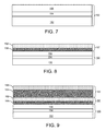
Turning now to FIGS. 7-13 , an example fabrication is discussed in connection with formation of the example of a SLCFET device structure that utilizes a combination of the techniques discussed in FIGS. 1-6 , such that the resultant structure has both a thicker middle layer to facilitate the utilization of fringing fields, and modulated doping concentrations for each channel based on channel width. FIG. 7 illustrates a cross-sectional view of an epitaxial structure in its early stages of fabrication. The epitaxial structure includes a base structure 150. As stated above, the base structure 150 can comprise a base layer 152, a nucleation layer 154 and a buffer layer 156 formed of a variety of different materials as described above.
It should be noted that for illustrative purposes, the bottom GaN is shown as being thinner than the thicker GaN. However, in practice, a back barrier structure of about 50 nm GaN is below the bottom AlGaN barrier followed by a 4% AlGaN back barrier underneath that to prevent current leakage under the gated ridges.
As illustrated in the cross-sectional view of FIG. 11 , an etch mask 176 is formed over the superlattice structure formed from the first, second and third heterostructures 157, 163, and 169, respectively. The etch mask 176 can be formed by depositing, patterning and developing a photoresist material layer over the superlattice structure, depositing a hard mask material, such as for example, a thick layer of metal (e.g., nickel) (about 300 Å) or the like in the patterned openings, and then removing the photoresist material layer to leave a resultant hard mask. The hard mask 176 provides covered regions that protect underylying areas of the superlattice structure, where the multi-ridge multi-channels will reside, and also covered regions that protect the source and drain regions (not shown). The mask 176 also includes openings 179 over the superlattice structure exposing a top layer of AlGaN 172 for forming underlying castellated non-channel openings 181 (see FIG. 12 ). Alternatively, a hard mask material such as an insulator material (e.g., silicon oxide (SiO2), silicon nitride (SiN), etc.) can be deposited over the superlattice structure followed by a depositing and patterning of photoresist material with a subsequent etching of the insulator material and stripping of the photoresist material to form the resultant mask 176.
What have been described above are examples of the invention. It is, of course, not possible to describe every conceivable combination of components or methodologies for purposes of describing the invention, but one of ordinary skill in the art will recognize that many further combinations and permutations of the invention are possible. Accordingly, the invention is intended to embrace all such alterations, modifications, and variations that fall within the scope of this application, including the appended claims.
Claims (6)
1. A method of forming a transistor device, the method comprising:
forming a superlattice structure comprising a plurality of heterostructures over a base structure by sequentially depositing each layer of the plurality of heterostructures over the base structure with one layer of each heterostructure being doped;
etching away openings in the superlattice structure over a channel region to form a castellated region in the channel region of alternating multichannel ridges with edges and nonchannel openings, wherein a parameter of at least one of corresponding parallel heterostructures of each of the alternating multichannel ridges is varied; and
performing a gate contact fill process to form a gate contact that wraps around and substantially surrounds the top and sides of each the alternating multichannel ridges along at least a portion of its depth and connects each one of the alternating multichannel ridges to one another through the non-channel openings.
2. The method of claim 1 , wherein the parameter is a dopant concentration.
3. The method of claim 1 , wherein the parameter is a dopant concentration for each heterostructure, such that longer width channels associated with a given heterostructure are doped with less dopant concentration than shorter width channels associated with a given heterostructure for each of the plurality of heterostructures to substantially equalize the pinch-off voltage of each channel of the SLCFET during operation.
4. The method of claim 1 , wherein the parameter is a thickness.
5. The method of claim 1 , wherein the parameter is a thickness, such that each inner heterostructure is formed with a greater thickness than a thickness of at least one of a top heterostructure and a bottom heterostructure for each of the alternating multichannel ridges.
6. The method of claim 1 , wherein the parameter is a thickness, such that every other inner heterostructure is formed with a greater thickness than a thickness of at least one of a top heterostructure and a bottom heterostructure for each of the alternating multichannel ridges.
Priority Applications (2)
| Application Number | Priority Date | Filing Date | Title |
|---|---|---|---|
| US15/222,039 US9711615B2 (en) | 2014-11-05 | 2016-07-28 | Multichannel devices with improved performance and methods of making the same |
| US15/624,445 US10084075B2 (en) | 2014-11-05 | 2017-06-15 | Methods of making multichannel devices with improved performance |
Applications Claiming Priority (2)
| Application Number | Priority Date | Filing Date | Title |
|---|---|---|---|
| US14/533,752 US9419120B2 (en) | 2014-11-05 | 2014-11-05 | Multichannel devices with improved performance |
| US15/222,039 US9711615B2 (en) | 2014-11-05 | 2016-07-28 | Multichannel devices with improved performance and methods of making the same |
Related Parent Applications (1)
| Application Number | Title | Priority Date | Filing Date |
|---|---|---|---|
| US14/533,752 Division US9419120B2 (en) | 2014-11-05 | 2014-11-05 | Multichannel devices with improved performance |
Related Child Applications (1)
| Application Number | Title | Priority Date | Filing Date |
|---|---|---|---|
| US15/624,445 Continuation US10084075B2 (en) | 2014-11-05 | 2017-06-15 | Methods of making multichannel devices with improved performance |
Publications (2)
| Publication Number | Publication Date |
|---|---|
| US20160336425A1 US20160336425A1 (en) | 2016-11-17 |
| US9711615B2 true US9711615B2 (en) | 2017-07-18 |
Family
ID=55853582
Family Applications (3)
| Application Number | Title | Priority Date | Filing Date |
|---|---|---|---|
| US14/533,752 Active US9419120B2 (en) | 2014-11-05 | 2014-11-05 | Multichannel devices with improved performance |
| US15/222,039 Active US9711615B2 (en) | 2014-11-05 | 2016-07-28 | Multichannel devices with improved performance and methods of making the same |
| US15/624,445 Active US10084075B2 (en) | 2014-11-05 | 2017-06-15 | Methods of making multichannel devices with improved performance |
Family Applications Before (1)
| Application Number | Title | Priority Date | Filing Date |
|---|---|---|---|
| US14/533,752 Active US9419120B2 (en) | 2014-11-05 | 2014-11-05 | Multichannel devices with improved performance |
Family Applications After (1)
| Application Number | Title | Priority Date | Filing Date |
|---|---|---|---|
| US15/624,445 Active US10084075B2 (en) | 2014-11-05 | 2017-06-15 | Methods of making multichannel devices with improved performance |
Country Status (1)
| Country | Link |
|---|---|
| US (3) | US9419120B2 (en) |
Cited By (3)
| Publication number | Priority date | Publication date | Assignee | Title |
|---|---|---|---|---|
| US10784341B2 (en) | 2019-01-21 | 2020-09-22 | Northrop Grumnian Systems Corporation | Castellated superjunction transistors |
| US10804387B1 (en) | 2019-03-21 | 2020-10-13 | Northrop Grumman Systems Corporation | Vertical superlattice transistors |
| US11342440B2 (en) | 2019-07-22 | 2022-05-24 | Northrop Grumman Systems Corporation | Passivated transistors |
Families Citing this family (11)
| Publication number | Priority date | Publication date | Assignee | Title |
|---|---|---|---|---|
| US9466679B2 (en) * | 2014-08-13 | 2016-10-11 | Northrop Grumman Systems Corporation | All around contact device and method of making the same |
| US10388746B2 (en) | 2017-07-06 | 2019-08-20 | Teledyne Scientific & Imaging, Llc | FET with buried gate structure |
| CN109427779B (en) * | 2017-08-22 | 2021-07-13 | 中芯国际集成电路制造(上海)有限公司 | Semiconductor structure and forming method thereof |
| US10658501B2 (en) | 2018-02-21 | 2020-05-19 | Mitsubishi Electric Research Laboratories, Inc. | Vertically stacked multichannel pyramid transistor |
| US10325982B1 (en) * | 2018-05-17 | 2019-06-18 | Northrop Grumman Systems Corporation | Drain ledge for self-aligned gate and independent channel region and drain-side ridges for SLCFET |
| CN110676167A (en) * | 2018-07-02 | 2020-01-10 | 西安电子科技大学 | AlInN/GaN high electron mobility transistor with multi-channel fin structure and manufacturing method |
| US11881511B2 (en) * | 2018-12-19 | 2024-01-23 | Intel Corporation | Superlattice FINFET with tunable drive current capability |
| US10879382B1 (en) | 2019-06-26 | 2020-12-29 | Northrop Grumman Systems Corporation | Enhancement mode saddle gate device |
| US11257941B2 (en) * | 2020-01-28 | 2022-02-22 | Infineon Technologies Austria Ag | High electron mobility transistor with doped semiconductor region in gate structure |
| US11967619B2 (en) * | 2020-09-16 | 2024-04-23 | Teledyne Scientific & Imaging, Llc | Laterally-gated transistors and lateral Schottky diodes with integrated lateral field plate structures |
| US20230299743A1 (en) * | 2022-03-17 | 2023-09-21 | Northrop Grumman Systems Corporation | Acoustic resonator filter system |
Citations (7)
| Publication number | Priority date | Publication date | Assignee | Title |
|---|---|---|---|---|
| US20020117681A1 (en) * | 2001-02-23 | 2002-08-29 | Weeks T. Warren | Gallium nitride material devices and methods including backside vias |
| US20060249748A1 (en) * | 2005-05-03 | 2006-11-09 | Nitronex Corporation | Gallium nitride material structures including substrates and methods associated with the same |
| US7692298B2 (en) | 2004-09-30 | 2010-04-06 | Sanken Electric Co., Ltd. | III-V nitride semiconductor device comprising a concave shottky contact and an ohmic contact |
| US20110127581A1 (en) | 2009-12-01 | 2011-06-02 | Bethoux Jean-Marc | Heterostructure for electronic power components, optoelectronic or photovoltaic components |
| US20120217512A1 (en) * | 2009-11-19 | 2012-08-30 | Philippe Renaud | Lateral power transistor device and method of manufacturing the same |
| US20140110759A1 (en) * | 2011-07-01 | 2014-04-24 | Panasonic Corporation | Semiconductor device |
| US20150123215A1 (en) | 2013-11-01 | 2015-05-07 | Samsung Electronics Co., Ltd. | Crystalline multiple-nanosheet iii-v channel fets |
-
2014
- 2014-11-05 US US14/533,752 patent/US9419120B2/en active Active
-
2016
- 2016-07-28 US US15/222,039 patent/US9711615B2/en active Active
-
2017
- 2017-06-15 US US15/624,445 patent/US10084075B2/en active Active
Patent Citations (7)
| Publication number | Priority date | Publication date | Assignee | Title |
|---|---|---|---|---|
| US20020117681A1 (en) * | 2001-02-23 | 2002-08-29 | Weeks T. Warren | Gallium nitride material devices and methods including backside vias |
| US7692298B2 (en) | 2004-09-30 | 2010-04-06 | Sanken Electric Co., Ltd. | III-V nitride semiconductor device comprising a concave shottky contact and an ohmic contact |
| US20060249748A1 (en) * | 2005-05-03 | 2006-11-09 | Nitronex Corporation | Gallium nitride material structures including substrates and methods associated with the same |
| US20120217512A1 (en) * | 2009-11-19 | 2012-08-30 | Philippe Renaud | Lateral power transistor device and method of manufacturing the same |
| US20110127581A1 (en) | 2009-12-01 | 2011-06-02 | Bethoux Jean-Marc | Heterostructure for electronic power components, optoelectronic or photovoltaic components |
| US20140110759A1 (en) * | 2011-07-01 | 2014-04-24 | Panasonic Corporation | Semiconductor device |
| US20150123215A1 (en) | 2013-11-01 | 2015-05-07 | Samsung Electronics Co., Ltd. | Crystalline multiple-nanosheet iii-v channel fets |
Cited By (4)
| Publication number | Priority date | Publication date | Assignee | Title |
|---|---|---|---|---|
| US10784341B2 (en) | 2019-01-21 | 2020-09-22 | Northrop Grumnian Systems Corporation | Castellated superjunction transistors |
| US10985243B2 (en) | 2019-01-21 | 2021-04-20 | Northrop Grumman Systems Corporation | Castellated superjunction transistors |
| US10804387B1 (en) | 2019-03-21 | 2020-10-13 | Northrop Grumman Systems Corporation | Vertical superlattice transistors |
| US11342440B2 (en) | 2019-07-22 | 2022-05-24 | Northrop Grumman Systems Corporation | Passivated transistors |
Also Published As
| Publication number | Publication date |
|---|---|
| US20160126340A1 (en) | 2016-05-05 |
| US20160336425A1 (en) | 2016-11-17 |
| US9419120B2 (en) | 2016-08-16 |
| US10084075B2 (en) | 2018-09-25 |
| US20170288045A1 (en) | 2017-10-05 |
Similar Documents
| Publication | Publication Date | Title |
|---|---|---|
| US10084075B2 (en) | Methods of making multichannel devices with improved performance | |
| US9755021B2 (en) | Integrated multichannel and single channel device structure and method of making the same | |
| EP2973722B1 (en) | Superlattice crenelated gate field effect transistor | |
| US9472634B2 (en) | All around contact device and method of making the same | |
| TWI624945B (en) | Recessed field plate transistor structures | |
| EP1747589B1 (en) | Methods of fabricating nitride-based transistors having regrown ohmic contact regions and nitride-based transistors having regrown ohmic contact regions | |
| US7592211B2 (en) | Methods of fabricating transistors including supported gate electrodes | |
| EP3326210B1 (en) | Semiconductor device and method for fabricating semiconductor device | |
| KR20220076516A (en) | Stepped Field Plates Proximate Conduction Channel and Related Manufacturing Methods | |
| CN109935630B (en) | Semiconductor device and method for manufacturing the same | |
| US11594625B2 (en) | III-N transistor structures with stepped cap layers | |
| KR20190112526A (en) | Heterostructure Field Effect Transistor and production method thereof | |
| TW202315119A (en) | Gan vertical trench mosfets and methods of manufacturing the same | |
| CN108831922B (en) | GaN HEMT device with GaAs and GaN composite channel and preparation method thereof | |
| US10804387B1 (en) | Vertical superlattice transistors | |
| US11342440B2 (en) | Passivated transistors | |
| US10985243B2 (en) | Castellated superjunction transistors | |
| CN111448667B (en) | Semiconductor device with enhanced transistor structure | |
| WO2023184129A1 (en) | Semiconductor device and method for manufacturing the same | |
| US20230420541A1 (en) | Multi-threshold voltage galium nitride high electron mobility transistor | |
| KR20230023659A (en) | Ohmic Contacts for Multi-Channel FETs | |
| CN117012825A (en) | Transistor with dielectric spacer and method of manufacturing the same | |
| CN114725192A (en) | 5G base station-oriented voltage-resistant radio frequency device and preparation method thereof |
Legal Events
| Date | Code | Title | Description |
|---|---|---|---|
| STCF | Information on status: patent grant |
Free format text: PATENTED CASE |
|
| CC | Certificate of correction | ||
| MAFP | Maintenance fee payment |
Free format text: PAYMENT OF MAINTENANCE FEE, 4TH YEAR, LARGE ENTITY (ORIGINAL EVENT CODE: M1551); ENTITY STATUS OF PATENT OWNER: LARGE ENTITY Year of fee payment: 4 |