US9698155B2 - Semiconductor devices and methods of fabricating the same - Google Patents
Semiconductor devices and methods of fabricating the same Download PDFInfo
- Publication number
- US9698155B2 US9698155B2 US14/563,432 US201414563432A US9698155B2 US 9698155 B2 US9698155 B2 US 9698155B2 US 201414563432 A US201414563432 A US 201414563432A US 9698155 B2 US9698155 B2 US 9698155B2
- Authority
- US
- United States
- Prior art keywords
- insulating layers
- forming
- layer
- substrate
- region
- Prior art date
- Legal status (The legal status is an assumption and is not a legal conclusion. Google has not performed a legal analysis and makes no representation as to the accuracy of the status listed.)
- Active
Links
- 239000004065 semiconductor Substances 0.000 title claims abstract description 73
- 238000000034 method Methods 0.000 title claims description 63
- 239000000758 substrate Substances 0.000 claims abstract description 62
- 239000010410 layer Substances 0.000 claims description 449
- 238000000926 separation method Methods 0.000 claims description 40
- 230000008569 process Effects 0.000 claims description 37
- 238000005530 etching Methods 0.000 claims description 26
- 229910052751 metal Inorganic materials 0.000 claims description 26
- 239000002184 metal Substances 0.000 claims description 26
- 239000012535 impurity Substances 0.000 claims description 21
- 239000000463 material Substances 0.000 claims description 15
- 238000004519 manufacturing process Methods 0.000 claims description 13
- 230000000149 penetrating effect Effects 0.000 claims description 10
- 229910021332 silicide Inorganic materials 0.000 claims description 9
- FVBUAEGBCNSCDD-UHFFFAOYSA-N silicide(4-) Chemical compound [Si-4] FVBUAEGBCNSCDD-UHFFFAOYSA-N 0.000 claims description 9
- 150000004767 nitrides Chemical class 0.000 claims description 8
- 239000002356 single layer Substances 0.000 claims 2
- 230000002093 peripheral effect Effects 0.000 description 20
- 238000010586 diagram Methods 0.000 description 10
- 229910052710 silicon Inorganic materials 0.000 description 10
- XUIMIQQOPSSXEZ-UHFFFAOYSA-N Silicon Chemical compound [Si] XUIMIQQOPSSXEZ-UHFFFAOYSA-N 0.000 description 9
- 230000015572 biosynthetic process Effects 0.000 description 9
- 239000010703 silicon Substances 0.000 description 9
- VYPSYNLAJGMNEJ-UHFFFAOYSA-N Silicium dioxide Chemical compound O=[Si]=O VYPSYNLAJGMNEJ-UHFFFAOYSA-N 0.000 description 8
- 230000000903 blocking effect Effects 0.000 description 8
- 229910052814 silicon oxide Inorganic materials 0.000 description 8
- 238000004891 communication Methods 0.000 description 7
- 230000010365 information processing Effects 0.000 description 6
- 230000010354 integration Effects 0.000 description 6
- 229910021420 polycrystalline silicon Inorganic materials 0.000 description 5
- 229920005591 polysilicon Polymers 0.000 description 5
- 101100481702 Arabidopsis thaliana TMK1 gene Proteins 0.000 description 4
- OKTJSMMVPCPJKN-UHFFFAOYSA-N Carbon Chemical compound [C] OKTJSMMVPCPJKN-UHFFFAOYSA-N 0.000 description 4
- 229910052581 Si3N4 Inorganic materials 0.000 description 4
- 238000003491 array Methods 0.000 description 4
- 238000005229 chemical vapour deposition Methods 0.000 description 4
- HQVNEWCFYHHQES-UHFFFAOYSA-N silicon nitride Chemical compound N12[Si]34N5[Si]62N3[Si]51N64 HQVNEWCFYHHQES-UHFFFAOYSA-N 0.000 description 4
- 238000005516 engineering process Methods 0.000 description 3
- 238000002513 implantation Methods 0.000 description 3
- 238000005468 ion implantation Methods 0.000 description 3
- 238000012545 processing Methods 0.000 description 3
- NBIIXXVUZAFLBC-UHFFFAOYSA-N Phosphoric acid Chemical compound OP(O)(O)=O NBIIXXVUZAFLBC-UHFFFAOYSA-N 0.000 description 2
- 229910052787 antimony Inorganic materials 0.000 description 2
- WATWJIUSRGPENY-UHFFFAOYSA-N antimony atom Chemical compound [Sb] WATWJIUSRGPENY-UHFFFAOYSA-N 0.000 description 2
- 238000000231 atomic layer deposition Methods 0.000 description 2
- 239000002041 carbon nanotube Substances 0.000 description 2
- 229910021393 carbon nanotube Inorganic materials 0.000 description 2
- 238000012937 correction Methods 0.000 description 2
- 230000009977 dual effect Effects 0.000 description 2
- 230000001747 exhibiting effect Effects 0.000 description 2
- 230000006870 function Effects 0.000 description 2
- 229910052732 germanium Inorganic materials 0.000 description 2
- GNPVGFCGXDBREM-UHFFFAOYSA-N germanium atom Chemical compound [Ge] GNPVGFCGXDBREM-UHFFFAOYSA-N 0.000 description 2
- 229910021389 graphene Inorganic materials 0.000 description 2
- 238000009413 insulation Methods 0.000 description 2
- 239000011229 interlayer Substances 0.000 description 2
- 239000002086 nanomaterial Substances 0.000 description 2
- 230000004044 response Effects 0.000 description 2
- 239000011669 selenium Substances 0.000 description 2
- 239000007787 solid Substances 0.000 description 2
- 238000003860 storage Methods 0.000 description 2
- 229910052714 tellurium Inorganic materials 0.000 description 2
- PORWMNRCUJJQNO-UHFFFAOYSA-N tellurium atom Chemical compound [Te] PORWMNRCUJJQNO-UHFFFAOYSA-N 0.000 description 2
- 229910006107 GeBiTe Inorganic materials 0.000 description 1
- 229910005872 GeSb Inorganic materials 0.000 description 1
- BUGBHKTXTAQXES-UHFFFAOYSA-N Selenium Chemical compound [Se] BUGBHKTXTAQXES-UHFFFAOYSA-N 0.000 description 1
- 229910000577 Silicon-germanium Inorganic materials 0.000 description 1
- GWEVSGVZZGPLCZ-UHFFFAOYSA-N Titan oxide Chemical compound O=[Ti]=O GWEVSGVZZGPLCZ-UHFFFAOYSA-N 0.000 description 1
- XHCLAFWTIXFWPH-UHFFFAOYSA-N [O-2].[O-2].[O-2].[O-2].[O-2].[V+5].[V+5] Chemical compound [O-2].[O-2].[O-2].[O-2].[O-2].[V+5].[V+5] XHCLAFWTIXFWPH-UHFFFAOYSA-N 0.000 description 1
- LEVVHYCKPQWKOP-UHFFFAOYSA-N [Si].[Ge] Chemical compound [Si].[Ge] LEVVHYCKPQWKOP-UHFFFAOYSA-N 0.000 description 1
- 229910052782 aluminium Inorganic materials 0.000 description 1
- 229910000147 aluminium phosphate Inorganic materials 0.000 description 1
- 239000002885 antiferromagnetic material Substances 0.000 description 1
- DQBAOWPVHRWLJC-UHFFFAOYSA-N barium(2+);dioxido(oxo)zirconium Chemical compound [Ba+2].[O-][Zr]([O-])=O DQBAOWPVHRWLJC-UHFFFAOYSA-N 0.000 description 1
- 229910052797 bismuth Inorganic materials 0.000 description 1
- 229910052796 boron Inorganic materials 0.000 description 1
- 229910052799 carbon Inorganic materials 0.000 description 1
- 230000015556 catabolic process Effects 0.000 description 1
- 239000000919 ceramic Substances 0.000 description 1
- 239000005387 chalcogenide glass Substances 0.000 description 1
- 230000008859 change Effects 0.000 description 1
- 150000001875 compounds Chemical class 0.000 description 1
- 239000011370 conductive nanoparticle Substances 0.000 description 1
- 239000004020 conductor Substances 0.000 description 1
- 238000013500 data storage Methods 0.000 description 1
- 238000000151 deposition Methods 0.000 description 1
- 230000008030 elimination Effects 0.000 description 1
- 238000003379 elimination reaction Methods 0.000 description 1
- 239000003302 ferromagnetic material Substances 0.000 description 1
- 229910000449 hafnium oxide Inorganic materials 0.000 description 1
- WIHZLLGSGQNAGK-UHFFFAOYSA-N hafnium(4+);oxygen(2-) Chemical compound [O-2].[O-2].[Hf+4] WIHZLLGSGQNAGK-UHFFFAOYSA-N 0.000 description 1
- 239000007943 implant Substances 0.000 description 1
- 229910052738 indium Inorganic materials 0.000 description 1
- WPYVAWXEWQSOGY-UHFFFAOYSA-N indium antimonide Chemical compound [Sb]#[In] WPYVAWXEWQSOGY-UHFFFAOYSA-N 0.000 description 1
- 238000002955 isolation Methods 0.000 description 1
- 229910000473 manganese(VI) oxide Inorganic materials 0.000 description 1
- 238000012986 modification Methods 0.000 description 1
- 230000004048 modification Effects 0.000 description 1
- 229910052759 nickel Inorganic materials 0.000 description 1
- PXHVJJICTQNCMI-UHFFFAOYSA-N nickel Substances [Ni] PXHVJJICTQNCMI-UHFFFAOYSA-N 0.000 description 1
- 229910000480 nickel oxide Inorganic materials 0.000 description 1
- 229910000484 niobium oxide Inorganic materials 0.000 description 1
- URLJKFSTXLNXLG-UHFFFAOYSA-N niobium(5+);oxygen(2-) Chemical compound [O-2].[O-2].[O-2].[O-2].[O-2].[Nb+5].[Nb+5] URLJKFSTXLNXLG-UHFFFAOYSA-N 0.000 description 1
- 230000003647 oxidation Effects 0.000 description 1
- 238000007254 oxidation reaction Methods 0.000 description 1
- 230000001590 oxidative effect Effects 0.000 description 1
- TWNQGVIAIRXVLR-UHFFFAOYSA-N oxo(oxoalumanyloxy)alumane Chemical compound O=[Al]O[Al]=O TWNQGVIAIRXVLR-UHFFFAOYSA-N 0.000 description 1
- GNRSAWUEBMWBQH-UHFFFAOYSA-N oxonickel Chemical compound [Ni]=O GNRSAWUEBMWBQH-UHFFFAOYSA-N 0.000 description 1
- 229910052760 oxygen Inorganic materials 0.000 description 1
- RVTZCBVAJQQJTK-UHFFFAOYSA-N oxygen(2-);zirconium(4+) Chemical compound [O-2].[O-2].[Zr+4] RVTZCBVAJQQJTK-UHFFFAOYSA-N 0.000 description 1
- 238000000059 patterning Methods 0.000 description 1
- 229910052711 selenium Inorganic materials 0.000 description 1
- 230000003068 static effect Effects 0.000 description 1
- VTMHSJONDPRVMJ-UHFFFAOYSA-N strontium barium(2+) oxygen(2-) zirconium(4+) Chemical compound [O--].[O--].[O--].[O--].[Sr++].[Zr+4].[Ba++] VTMHSJONDPRVMJ-UHFFFAOYSA-N 0.000 description 1
- VEALVRVVWBQVSL-UHFFFAOYSA-N strontium titanate Chemical compound [Sr+2].[O-][Ti]([O-])=O VEALVRVVWBQVSL-UHFFFAOYSA-N 0.000 description 1
- 229910014031 strontium zirconium oxide Inorganic materials 0.000 description 1
- CZXRMHUWVGPWRM-UHFFFAOYSA-N strontium;barium(2+);oxygen(2-);titanium(4+) Chemical compound [O-2].[O-2].[O-2].[O-2].[Ti+4].[Sr+2].[Ba+2] CZXRMHUWVGPWRM-UHFFFAOYSA-N 0.000 description 1
- FCCTVDGKMTZSPU-UHFFFAOYSA-N strontium;dioxido(oxo)zirconium Chemical compound [Sr+2].[O-][Zr]([O-])=O FCCTVDGKMTZSPU-UHFFFAOYSA-N 0.000 description 1
- 239000003826 tablet Substances 0.000 description 1
- 229910052718 tin Inorganic materials 0.000 description 1
- 229910052719 titanium Inorganic materials 0.000 description 1
- 239000010936 titanium Substances 0.000 description 1
- OGIDPMRJRNCKJF-UHFFFAOYSA-N titanium oxide Inorganic materials [Ti]=O OGIDPMRJRNCKJF-UHFFFAOYSA-N 0.000 description 1
- 229910000314 transition metal oxide Inorganic materials 0.000 description 1
- 229910001935 vanadium oxide Inorganic materials 0.000 description 1
- 229910001928 zirconium oxide Inorganic materials 0.000 description 1
Images


Classifications
-
- H—ELECTRICITY
- H10—SEMICONDUCTOR DEVICES; ELECTRIC SOLID-STATE DEVICES NOT OTHERWISE PROVIDED FOR
- H10B—ELECTRONIC MEMORY DEVICES
- H10B43/00—EEPROM devices comprising charge-trapping gate insulators
- H10B43/20—EEPROM devices comprising charge-trapping gate insulators characterised by three-dimensional arrangements, e.g. with cells on different height levels
- H10B43/23—EEPROM devices comprising charge-trapping gate insulators characterised by three-dimensional arrangements, e.g. with cells on different height levels with source and drain on different levels, e.g. with sloping channels
- H10B43/27—EEPROM devices comprising charge-trapping gate insulators characterised by three-dimensional arrangements, e.g. with cells on different height levels with source and drain on different levels, e.g. with sloping channels the channels comprising vertical portions, e.g. U-shaped channels
-
- H—ELECTRICITY
- H01—ELECTRIC ELEMENTS
- H01L—SEMICONDUCTOR DEVICES NOT COVERED BY CLASS H10
- H01L21/00—Processes or apparatus adapted for the manufacture or treatment of semiconductor or solid state devices or of parts thereof
- H01L21/70—Manufacture or treatment of devices consisting of a plurality of solid state components formed in or on a common substrate or of parts thereof; Manufacture of integrated circuit devices or of parts thereof
- H01L21/71—Manufacture of specific parts of devices defined in group H01L21/70
- H01L21/768—Applying interconnections to be used for carrying current between separate components within a device comprising conductors and dielectrics
-
- H01L27/11582—
-
- H—ELECTRICITY
- H01—ELECTRIC ELEMENTS
- H01L—SEMICONDUCTOR DEVICES NOT COVERED BY CLASS H10
- H01L23/00—Details of semiconductor or other solid state devices
- H01L23/48—Arrangements for conducting electric current to or from the solid state body in operation, e.g. leads, terminal arrangements ; Selection of materials therefor
-
- H—ELECTRICITY
- H01—ELECTRIC ELEMENTS
- H01L—SEMICONDUCTOR DEVICES NOT COVERED BY CLASS H10
- H01L23/00—Details of semiconductor or other solid state devices
- H01L23/52—Arrangements for conducting electric current within the device in operation from one component to another, i.e. interconnections, e.g. wires, lead frames
- H01L23/538—Arrangements for conducting electric current within the device in operation from one component to another, i.e. interconnections, e.g. wires, lead frames the interconnection structure between a plurality of semiconductor chips being formed on, or in, insulating substrates
- H01L23/5384—Conductive vias through the substrate with or without pins, e.g. buried coaxial conductors
-
- H—ELECTRICITY
- H01—ELECTRIC ELEMENTS
- H01L—SEMICONDUCTOR DEVICES NOT COVERED BY CLASS H10
- H01L27/00—Devices consisting of a plurality of semiconductor or other solid-state components formed in or on a common substrate
- H01L27/02—Devices consisting of a plurality of semiconductor or other solid-state components formed in or on a common substrate including semiconductor components specially adapted for rectifying, oscillating, amplifying or switching and having at least one potential-jump barrier or surface barrier; including integrated passive circuit elements with at least one potential-jump barrier or surface barrier
- H01L27/04—Devices consisting of a plurality of semiconductor or other solid-state components formed in or on a common substrate including semiconductor components specially adapted for rectifying, oscillating, amplifying or switching and having at least one potential-jump barrier or surface barrier; including integrated passive circuit elements with at least one potential-jump barrier or surface barrier the substrate being a semiconductor body
- H01L27/06—Devices consisting of a plurality of semiconductor or other solid-state components formed in or on a common substrate including semiconductor components specially adapted for rectifying, oscillating, amplifying or switching and having at least one potential-jump barrier or surface barrier; including integrated passive circuit elements with at least one potential-jump barrier or surface barrier the substrate being a semiconductor body including a plurality of individual components in a non-repetitive configuration
- H01L27/0688—Integrated circuits having a three-dimensional layout
-
- H01L27/11556—
-
- H01L27/11565—
-
- H01L27/2409—
-
- H01L27/2481—
-
- H01L27/249—
-
- H—ELECTRICITY
- H01—ELECTRIC ELEMENTS
- H01L—SEMICONDUCTOR DEVICES NOT COVERED BY CLASS H10
- H01L29/00—Semiconductor devices adapted for rectifying, amplifying, oscillating or switching, or capacitors or resistors with at least one potential-jump barrier or surface barrier, e.g. PN junction depletion layer or carrier concentration layer; Details of semiconductor bodies or of electrodes thereof ; Multistep manufacturing processes therefor
- H01L29/66—Types of semiconductor device ; Multistep manufacturing processes therefor
- H01L29/68—Types of semiconductor device ; Multistep manufacturing processes therefor controllable by only the electric current supplied, or only the electric potential applied, to an electrode which does not carry the current to be rectified, amplified or switched
- H01L29/76—Unipolar devices, e.g. field effect transistors
- H01L29/772—Field effect transistors
- H01L29/78—Field effect transistors with field effect produced by an insulated gate
- H01L29/7827—Vertical transistors
-
- H—ELECTRICITY
- H10—SEMICONDUCTOR DEVICES; ELECTRIC SOLID-STATE DEVICES NOT OTHERWISE PROVIDED FOR
- H10B—ELECTRONIC MEMORY DEVICES
- H10B41/00—Electrically erasable-and-programmable ROM [EEPROM] devices comprising floating gates
- H10B41/20—Electrically erasable-and-programmable ROM [EEPROM] devices comprising floating gates characterised by three-dimensional arrangements, e.g. with cells on different height levels
- H10B41/23—Electrically erasable-and-programmable ROM [EEPROM] devices comprising floating gates characterised by three-dimensional arrangements, e.g. with cells on different height levels with source and drain on different levels, e.g. with sloping channels
- H10B41/27—Electrically erasable-and-programmable ROM [EEPROM] devices comprising floating gates characterised by three-dimensional arrangements, e.g. with cells on different height levels with source and drain on different levels, e.g. with sloping channels the channels comprising vertical portions, e.g. U-shaped channels
-
- H—ELECTRICITY
- H10—SEMICONDUCTOR DEVICES; ELECTRIC SOLID-STATE DEVICES NOT OTHERWISE PROVIDED FOR
- H10B—ELECTRONIC MEMORY DEVICES
- H10B43/00—EEPROM devices comprising charge-trapping gate insulators
- H10B43/10—EEPROM devices comprising charge-trapping gate insulators characterised by the top-view layout
-
- H—ELECTRICITY
- H10—SEMICONDUCTOR DEVICES; ELECTRIC SOLID-STATE DEVICES NOT OTHERWISE PROVIDED FOR
- H10B—ELECTRONIC MEMORY DEVICES
- H10B63/00—Resistance change memory devices, e.g. resistive RAM [ReRAM] devices
- H10B63/20—Resistance change memory devices, e.g. resistive RAM [ReRAM] devices comprising selection components having two electrodes, e.g. diodes
-
- H—ELECTRICITY
- H10—SEMICONDUCTOR DEVICES; ELECTRIC SOLID-STATE DEVICES NOT OTHERWISE PROVIDED FOR
- H10B—ELECTRONIC MEMORY DEVICES
- H10B63/00—Resistance change memory devices, e.g. resistive RAM [ReRAM] devices
- H10B63/80—Arrangements comprising multiple bistable or multi-stable switching components of the same type on a plane parallel to the substrate, e.g. cross-point arrays
- H10B63/84—Arrangements comprising multiple bistable or multi-stable switching components of the same type on a plane parallel to the substrate, e.g. cross-point arrays arranged in a direction perpendicular to the substrate, e.g. 3D cell arrays
- H10B63/845—Arrangements comprising multiple bistable or multi-stable switching components of the same type on a plane parallel to the substrate, e.g. cross-point arrays arranged in a direction perpendicular to the substrate, e.g. 3D cell arrays the switching components being connected to a common vertical conductor
-
- H—ELECTRICITY
- H10—SEMICONDUCTOR DEVICES; ELECTRIC SOLID-STATE DEVICES NOT OTHERWISE PROVIDED FOR
- H10N—ELECTRIC SOLID-STATE DEVICES NOT OTHERWISE PROVIDED FOR
- H10N70/00—Solid-state devices without a potential-jump barrier or surface barrier, and specially adapted for rectifying, amplifying, oscillating or switching
- H10N70/20—Multistable switching devices, e.g. memristors
- H10N70/231—Multistable switching devices, e.g. memristors based on solid-state phase change, e.g. between amorphous and crystalline phases, Ovshinsky effect
-
- H—ELECTRICITY
- H10—SEMICONDUCTOR DEVICES; ELECTRIC SOLID-STATE DEVICES NOT OTHERWISE PROVIDED FOR
- H10N—ELECTRIC SOLID-STATE DEVICES NOT OTHERWISE PROVIDED FOR
- H10N70/00—Solid-state devices without a potential-jump barrier or surface barrier, and specially adapted for rectifying, amplifying, oscillating or switching
- H10N70/801—Constructional details of multistable switching devices
- H10N70/881—Switching materials
- H10N70/883—Oxides or nitrides
- H10N70/8833—Binary metal oxides, e.g. TaOx
-
- H—ELECTRICITY
- H01—ELECTRIC ELEMENTS
- H01L—SEMICONDUCTOR DEVICES NOT COVERED BY CLASS H10
- H01L2924/00—Indexing scheme for arrangements or methods for connecting or disconnecting semiconductor or solid-state bodies as covered by H01L24/00
-
- H—ELECTRICITY
- H01—ELECTRIC ELEMENTS
- H01L—SEMICONDUCTOR DEVICES NOT COVERED BY CLASS H10
- H01L2924/00—Indexing scheme for arrangements or methods for connecting or disconnecting semiconductor or solid-state bodies as covered by H01L24/00
- H01L2924/0001—Technical content checked by a classifier
- H01L2924/0002—Not covered by any one of groups H01L24/00, H01L24/00 and H01L2224/00
-
- H01L45/04—
-
- H01L45/06—
-
- H01L45/1226—
-
- H01L45/144—
-
- H01L45/146—
-
- H01L45/147—
-
- H01L45/148—
-
- H—ELECTRICITY
- H10—SEMICONDUCTOR DEVICES; ELECTRIC SOLID-STATE DEVICES NOT OTHERWISE PROVIDED FOR
- H10N—ELECTRIC SOLID-STATE DEVICES NOT OTHERWISE PROVIDED FOR
- H10N70/00—Solid-state devices without a potential-jump barrier or surface barrier, and specially adapted for rectifying, amplifying, oscillating or switching
- H10N70/20—Multistable switching devices, e.g. memristors
-
- H—ELECTRICITY
- H10—SEMICONDUCTOR DEVICES; ELECTRIC SOLID-STATE DEVICES NOT OTHERWISE PROVIDED FOR
- H10N—ELECTRIC SOLID-STATE DEVICES NOT OTHERWISE PROVIDED FOR
- H10N70/00—Solid-state devices without a potential-jump barrier or surface barrier, and specially adapted for rectifying, amplifying, oscillating or switching
- H10N70/801—Constructional details of multistable switching devices
- H10N70/821—Device geometry
- H10N70/823—Device geometry adapted for essentially horizontal current flow, e.g. bridge type devices
-
- H—ELECTRICITY
- H10—SEMICONDUCTOR DEVICES; ELECTRIC SOLID-STATE DEVICES NOT OTHERWISE PROVIDED FOR
- H10N—ELECTRIC SOLID-STATE DEVICES NOT OTHERWISE PROVIDED FOR
- H10N70/00—Solid-state devices without a potential-jump barrier or surface barrier, and specially adapted for rectifying, amplifying, oscillating or switching
- H10N70/801—Constructional details of multistable switching devices
- H10N70/881—Switching materials
- H10N70/882—Compounds of sulfur, selenium or tellurium, e.g. chalcogenides
- H10N70/8828—Tellurides, e.g. GeSbTe
-
- H—ELECTRICITY
- H10—SEMICONDUCTOR DEVICES; ELECTRIC SOLID-STATE DEVICES NOT OTHERWISE PROVIDED FOR
- H10N—ELECTRIC SOLID-STATE DEVICES NOT OTHERWISE PROVIDED FOR
- H10N70/00—Solid-state devices without a potential-jump barrier or surface barrier, and specially adapted for rectifying, amplifying, oscillating or switching
- H10N70/801—Constructional details of multistable switching devices
- H10N70/881—Switching materials
- H10N70/883—Oxides or nitrides
- H10N70/8836—Complex metal oxides, e.g. perovskites, spinels
-
- H—ELECTRICITY
- H10—SEMICONDUCTOR DEVICES; ELECTRIC SOLID-STATE DEVICES NOT OTHERWISE PROVIDED FOR
- H10N—ELECTRIC SOLID-STATE DEVICES NOT OTHERWISE PROVIDED FOR
- H10N70/00—Solid-state devices without a potential-jump barrier or surface barrier, and specially adapted for rectifying, amplifying, oscillating or switching
- H10N70/801—Constructional details of multistable switching devices
- H10N70/881—Switching materials
- H10N70/884—Other compounds of groups 13-15, e.g. elemental or compound semiconductors
Definitions
- the present inventive concepts relates to a semiconductor device, more particularly, to a vertical-type semiconductor device and a method of manufacturing the same.
- a density of integration in memory devices is an important factor in determining the prices of products.
- 2D Two-Dimensional
- a density of integration is mainly determined by the occupied area of memory cells, which is affected by the level of fine pattern forming technology.
- this fine pattern forming technology performed by high-cost equipments, may limit a density of integration in 2D semiconductor memory devices.
- 3D memory devices including memory cells three-dimensionally arranged have been proposed.
- a process technology which reduces manufacturing costs per bit relative to 2D memory devices and secures reliable product characteristics is required.
- a semiconductor device includes a plurality of horizontal electrodes vertically stacked on a substrate.
- a plurality of first insulating layers each is disposed between a corresponding pair of the plurality of horizontal electrodes.
- a plurality of second insulating layers each is disposed between a corresponding pair of the plurality of first insulating layers and is disposed at the same vertical level as a corresponding one of the plurality of horizontal electrodes.
- a contact structure penetrates the first and second insulating layers. The contact structure is in contact with the first insulating layers and the second insulating layers.
- a semiconductor device includes a stack structure disposed on a substrate.
- the stack structure includes four or more first insulating layers and four or more second insulating layers sequentially stacked one over the other.
- a contact structure penetrates the stack structure.
- Four or more horizontal electrodes are extended between the first insulating layers.
- the first insulating layers and the second insulating layers are in contact with the contact structure.
- the first insulating layers include different materials from the second insulating layers.
- a plurality of first insulating layers and a plurality of second insulating layers are alternately stacked on a substrate.
- Spaces are formed between the plurality of second insulating layers by partially etching the plurality of second insulating layers.
- the spaces are defined by the plurality of first insulating layers and remaining portions of the plurality of second insulating layers.
- Horizontal electrodes are disposed in the spaces.
- a contact structure penetrates the plurality of first insulating layers and the remaining portions of the plurality of second insulating layers.
- a semiconductor device includes a plurality of first insulating layers and a plurality of second layers alternately and vertically stacked on a substrate.
- Each of the plurality of second layers includes a horizontal electrode horizontally separated by a second insulating layer.
- a contact plug penetrates the plurality of first insulating layers and the second insulating layer of the plurality of second layers.
- FIG. 1 is a block diagram illustrating a semiconductor device according to an exemplary embodiment of the inventive concept
- FIG. 2 is a block diagram schematically illustrating a memory cell array of FIG. 1 .
- FIG. 3 is a plan view illustrating a semiconductor device and a method of fabricating the same, according to an exemplary embodiment of the inventive concept.
- FIGS. 4 through 11 are sectional views taken along lines A-A′ and B-B′ of FIG. 3 .
- FIG. 12 is a plan view illustrating a semiconductor device and a method of fabricating the same, according to an exemplary embodiment of the inventive concept.
- FIG. 13 is a sectional view taken along lines A-A′ and B-B′ of FIG. 12 .
- FIG. 14 is a plan view illustrating a semiconductor device and a method of fabricating the same, according to an exemplary embodiment of the inventive concept.
- FIG. 15 is a sectional view taken along lines A-A′ and B-B′ of FIG. 14 .
- FIGS. 16 through 19 are plan views illustrating a process of forming residual insulating layers, according to some exemplary embodiments of the inventive concept.
- FIGS. 20 through 21 are plan views illustrating a process of forming residual insulating layers, according to an exemplary embodiment of the inventive concept.
- FIG. 22 is a plan view illustrating a semiconductor device and a method of fabricating the same, according to an exemplary embodiment of the inventive concept.
- FIGS. 23 through 25 are sectional views taken along lines A-A′ and B-B′ of FIG. 22 .
- FIGS. 26 and 27 are sectional views illustrating a process of forming a first conductive region according to an exemplary embodiment of the inventive concept, taken along lines A-A′ and B-B′ of FIG. 3 .
- FIGS. 28 and 29 are sectional views illustrating a process of forming a first conductive region according to an exemplary embodiment of the inventive concept, taken along lines A-A′ and B-B′ of FIG. 3 .
- FIGS. 30A through 30D are sectional views illustrating memory elements according to some exemplary embodiments of the inventive concept.
- FIGS. 31A through 31D are sectional views illustrating memory elements according to exemplary embodiments of the inventive concept.
- FIG. 32 is a plan view illustrating an example of interconnection between conductive lines, according to an exemplary embodiment of the inventive concept.
- FIGS. 33 and 35 are sectional views taken along a line A-A′ of FIG. 32
- FIGS. 34 and 36 are sectional views taken along a line B-B′ of FIG. 32 .
- FIG. 37 is a plan view illustrating an example of interconnection between conductive lines, according to an exemplary embodiment of the inventive concept.
- FIGS. 38 and 40 are sectional views taken along a line A-A′ of FIG. 37
- FIGS. 39 and 41 are sectional views taken along a line B-B′ of FIG. 37 .
- FIGS. 42 and 43 are plan views illustrating examples of interconnection between conductive lines, according to exemplary embodiments of the inventive concept.
- FIG. 44 is a plan view illustrating a memory cell region and a pad contact region, according to an exemplary embodiment of the inventive concept.
- FIG. 45 is a sectional view taken along a line C-C′ of FIG. 44 .
- FIGS. 46 and 47 are sectional views illustrating a process of forming a pad contact region and a peripheral circuit region, according to an exemplary embodiment of the inventive concept.
- FIG. 48 is a schematic block diagram illustrating an example of memory systems including a semiconductor device according to an exemplary embodiment of the inventive concept.
- FIG. 49 is a schematic block diagram illustrating an example of memory cards including a semiconductor device according to an exemplary embodiment of the inventive concept.
- FIG. 50 is a schematic block diagram illustrating an example of information processing systems including a semiconductor device according to an exemplary embodiment of the inventive concept.
- inventive concepts will be described below in more detail with reference to the accompanying drawings.
- inventive concepts may, however, be embodied in different forms and should not be construed as limited to the embodiments set forth herein; rather, these exemplary embodiments are provided so that this disclosure will be thorough and complete, and will fully convey the concept of example embodiments to those of ordinary skill in the art.
- the thicknesses of layers and regions are exaggerated for clarity.
- Like reference numerals denote like elements throughout the specification and drawings, and thus their description will be omitted.
- first”, “second”, etc. may be used herein to describe various elements, components, regions, layers and/or sections, these elements, components, regions, layers and/or sections should not be limited by these terms. These terms are only used to distinguish one element, component, region, layer or section from another element, component, region, layer or section. Thus, a first element, component, region, layer or section discussed below could be termed a second element, component, region, layer or section without departing from the teachings of example embodiments.
- spatially relative terms such as “beneath,” “below,” “lower,” “above,” “upper” and the like, may be used herein for ease of description to describe one element or feature's relationship to another element(s) or feature(s) as illustrated in the figures. It will be understood that the spatially relative terms are intended to encompass different orientations of the device in use or operation in addition to the orientation depicted in the figures. For example, if the device in the figures is turned over, elements described as “below” or “beneath” other elements or features would then be oriented “above” the other elements or features. Thus, the exemplary term “below” may encompass both an orientation of above and below. The device may be otherwise oriented (rotated 90 degrees or at other orientations) and the spatially relative descriptors used herein interpreted accordingly.
- Example embodiments of the inventive concept are described herein with reference to cross-sectional illustrations that are schematic illustrations of idealized embodiments (and intermediate structures) of exemplary embodiments. As such, variations from the shapes of the illustrations as a result, for example, of manufacturing techniques and/or tolerances, are to be expected. Thus, exemplary embodiments of the inventive concepts should not be construed as limited to the particular shapes of regions illustrated herein but are to include deviations in shapes that result, for example, from manufacturing. For example, an implanted region illustrated as a rectangle may have rounded or curved features and/or a gradient of implant concentration at its edges rather than a binary change from implanted to non-implanted region.
- a buried region formed by implantation may result in some implantation in the region between the buried region and the surface through which the implantation takes place.
- the regions illustrated in the figures are schematic in nature and their shapes are not intended to illustrate the actual shape of a region of a device and are not intended to limit the scope of example embodiments.
- FIG. 1 is a block diagram illustrating a semiconductor device according to an exemplary embodiment of the inventive concept.
- a nonvolatile memory device according to an exemplary embodiment of the inventive concept includes a memory cell array 10 , an address decoder 20 , a read/write circuit 30 , a data input/output circuit 40 , and a control logic 50 .
- the memory cell array 10 is connected to the address decoder 20 through a plurality of word lines WL, and be connected to the read/write circuit 30 through a plurality of bit lines BL.
- the memory cell array 10 includes a plurality of memory cells (not shown).
- the memory cell array 10 may store one or more bits in each cell.
- the address decoder 20 is connected to the memory cell array 10 through the word lines WL.
- the address decoder 20 operates according to the control of the control logic 50 .
- the address decoder 20 may receive an address ADDR from the outside.
- the address decoder 20 decodes a row address among the received address ADDR to select a corresponding word line from among the word lines WL.
- the address decoder 20 decodes a column address among the address ADDR and transfers the decoded column address to the read/write circuit 30 .
- the address decoder 20 may include elements such as a row decoder, a column decoder and an address buffer.
- the read/write circuit 30 is connected to the memory cell array 10 through the bit line BL.
- the read/write circuit 30 may be connected to the data input/output circuit 40 through the data lines DL.
- the read/write circuit 30 may operate according to the control of the control logic 50 .
- the read/write circuit 30 receives the decoded column address from the address decoder 20 , and selects a bit line BL using the decoded column address.
- the read/write circuit 30 receives data from the data input/output circuit 40 and writes the received data in the memory cell array 10 .
- the read/write circuit 30 reads data from the memory cell array 10 and transfers the read data to the data input/output circuit 40 .
- the read/write circuit 30 reads data from a first storage region (not shown) of the memory cell array 10 , and writes the read data in a second storage region (not shown) of the memory cell array 10 .
- the read/write circuit 30 may perform a copy-back operation.
- the read/write circuit 30 may include elements which include a page buffer (not shown) or a page register (not shown) and a column selection circuit (not shown). As another example, the read/write circuit 30 may include elements which include a sensing amplifier, a write driver and a column selection circuit.
- the data input/output circuit 40 is connected to the read/write circuit 30 through the data lines DL.
- the data input/output circuit 40 operates according to the control of the control logic 50 .
- the data input/output circuit 40 exchanges data DATA with the outside.
- the data input/output circuit 40 transfers the data DATA to the read/write circuit 30 through the data lines DL.
- the data input/output circuit 40 outputs the data DATA, which is transferred from the read/write circuit 30 through the data lines DL, to the outside.
- the data input/output circuit 40 may include a data buffer (not shown).
- the control logic 50 is connected to the address decoder 20 , the read/write circuit 30 and the data input/output circuit 40 .
- the control logic 50 controls the operation of a 3D semiconductor device.
- the control logic 50 operates in response to a control signal CTRL transferred from the outside.
- FIG. 2 is a block diagram illustrating as an example of the memory cell array 10 of FIG. 1 .
- the memory cell array 10 may include a plurality of memory blocks BLK 1 to BLKh.
- Each of the memory blocks BLK 1 to BLKh may have a vertical 3D structure.
- the each of the memory blocks BLK 1 to BLKh may include structures that are extended in first to third directions intersecting each other.
- the each of the memory blocks BLK 1 to BLKh includes a plurality of cell strings (not shown) that are extended in the third direction.
- FIG. 3 is a plan view illustrating a semiconductor device according to an exemplary embodiment of the inventive concept.
- FIGS. 4 through 11 are sectional views taken along lines A-A′ and B-B′ of FIG. 3 .
- the substrate 100 may include a silicon substrate, a germanium substrate, or a silicon-germanium substrate.
- the substrate 100 may include a doped region having a first conductivity type.
- the first conductivity type may be a p-type.
- a first conductive region 101 is provided in the substrate 100 .
- the first conductive region 101 may be configured to apply a specific voltage to the substrate 100 .
- the first conductive region 101 may be a doped region provided in an upper region of the substrate 100 .
- the first conductive region 101 may have the same conductivity type as the substrate 100 and have a doping concentration higher than the substrate 100 .
- the first conductive region 101 may have a line shape extending along an x direction.
- the first conductive region 101 may be formed by an ion implantation process.
- a buffer insulating layer 105 is formed on the substrate 100 .
- the buffer insulating layer 105 may include a silicon oxide layer.
- the buffer insulating layer 105 may be formed using a thermal oxidation process.
- Second insulating layers 110 and first insulating layers 120 are alternately stacked on the buffer insulating layer 105 .
- the numbers of the first insulating layers 120 and the second insulating layers 110 may be four or more.
- a pair of the first and second insulating layers 120 and 110 may be repeatedly formed ten or more times.
- the second insulating layers 110 and the first insulating layers 120 may include materials having etch selectivity with respect to each other.
- the first insulating layers 120 may include materials having a much lower etch rate than that of the second insulating layers 110 to the specific etch recipe.
- the etch selectivity may be quantitatively expressed in terms of a ratio of an etch rate of the second insulating layers 110 to that of the first insulating layers 120 .
- the second insulating layers 110 may include materials having etch selectivity of 1:10 to 1:200 (or 1:30 to 1:100) with respect to the first insulating layers 120 .
- the second insulating layers 110 may include a silicon nitride layer, a silicon oxynitride layer, and/or a polysilicon layer.
- the first insulating layers 120 may include a silicon oxide layer.
- the insulating layers 110 and 120 may be formed by a chemical vapor deposition (CVD).
- cell holes 125 are formed through the insulating layers 110 and 120 to expose the substrate 100 using an anisotropic etching process.
- a semiconductor layer 130 and a gap-fill insulating layer 140 are sequentially formed to fill each of the cell holes 125 .
- the semiconductor layer 130 may be conformally formed in such a manner that the cell holes 125 are not completely filled with the semiconductor layer 130 .
- the semiconductor layer 130 may be formed to conformally cover sidewalls of the insulating layers 110 and 120 and a top surface of the substrate 100 .
- the sidewalls of the insulating layers 110 and 120 and the top surface of the substrate 100 define the cell holes 125 .
- the gap-fill insulating layer 140 may be formed to fill the cell holes 125 provided with the semiconductor layer 130 .
- the semiconductor layer 130 and the gap-fill insulating layer 140 may cover a top surface of an uppermost one of the first insulating layers 120 .
- the semiconductor layer 130 may fill the cell holes 125 .
- the gap-fill insulating layer 140 need not be provided.
- the semiconductor layer 130 may include a polysilicon layer having the first conductivity type.
- the gap-fill insulating layer 140 may include a silicon oxide layer or a silicon oxynitride layer.
- the semiconductor layer 130 may include a conductive layer (e.g., a doped semiconductor layer, a metal layer, a conductive metal nitride layer, a silicide layer), or a nano structure (e.g., a carbon nanotube or a graphene layer).
- the semiconductor layer 130 and the gap-fill insulating layer 140 may be formed using a chemical vapor deposition process or an atomic layer deposition (ALD) process.
- ALD atomic layer deposition
- separation regions 126 may be formed to expose the substrate 100 through the gap-fill insulating layer 140 , and the insulating layers 110 and 120 .
- the separation regions 126 may be delimited by sidewalls of the insulating layers 110 and 120 and the top surface of the substrate 100 .
- the separation regions 126 may be formed to have a trench-shaped structure extending along the x direction.
- the second insulating layers 110 exposed by the separation regions 126 may be partially removed to form recess regions 144 .
- the recess regions 144 may be empty regions produced by removing the second insulating layers 110 .
- the formation of the recess regions 144 may be performed using an etching solution containing a phosphoric acid.
- Each of the recess regions 144 may be formed to partially expose a sidewall of the semiconductor layer 130 .
- portions of the second insulating layers 110 may remain between the first insulating layers 120 , even after the formation of the recess regions 144 .
- the residual insulating layers 111 may be formed to be overlapped with the first conductive region 101 , in plan view. The formation of the residual insulating layers 111 will be described in more detail with reference to FIGS. 16 through 21 .
- a memory element 135 and horizontal electrodes PG are formed in the recess regions 144 .
- a memory layer (not shown) and a conductive layer (not shown) may be sequentially formed in the recess regions 144 and in the separation region 126 .
- the memory element 135 and horizontal electrodes PG may be formed by removing portions of the memory layer and the conductive layer located in the separation region 126 or at the outside of the recess regions 144 .
- the memory element 135 may include a tunnel insulating layer (not shown), a charge storing layer (not shown) on the tunnel insulating layer, and a blocking insulating layer (not shown) on the charge storing layer.
- the memory element 135 may be a variable resistance pattern.
- the horizontal electrodes PG are vertically spaced apart from each other by the first insulating layers 120 .
- the horizontal electrodes PG may include a doped silicon layer, a metal layer, a metal silicide layer, and/or a conductive metal nitride layer.
- the memory element 135 and the horizontal electrodes PG will be described in more detail with reference to FIGS. 30A through 30D and FIGS. 31A through 31D .
- Impurity regions 102 are formed in an upper portion of the substrate 100 exposed by the separation regions 126 .
- the impurity regions 102 may include a different conductivity type (e.g., a second conductivity type or n-type) from and having a higher concentration than the substrate 100 .
- the impurity regions 102 may be of a line shape extending along the x direction.
- the impurity regions 102 may serve as common source lines of the semiconductor device.
- separation layers 145 are formed to fill the separation regions 126 .
- an insulating layer (not shown) may be formed in the separation regions 126 and may be formed on an upper surface of the gap-fill insulating layer 140 of FIG. 9 .
- the insulating layer may include a silicon oxide layer and/or a silicon oxynitride layer.
- a planarization process may be performed to remove the insulating layer (now shown), the gap-fill insulating layer 140 of FIG. 9 and the semiconductor layer 130 of FIG. 9 . In such a case, the separation layers 145 are left in the separation regions 126 and the gap-fill insulating layer 140 of FIG.
- the gap-fill insulating layer 140 of FIG. 9 is localized in each of the cell holes 125 to form the gap-fill insulating patterns 141 .
- Second conductive regions 132 are formed on the cell pillars PL. For example, upper portions of the cell pillars PL may be removed, and a doped polysilicon layer or a metal layer may be deposited.
- the second conductive regions 132 may include a doped pattern of an n-type semiconductor.
- the second conductive regions 132 may serve as drain regions of the semiconductor device.
- a first interlayered insulating layer 114 is formed to cover the second conductive regions 132 using a chemical vapor deposition.
- the first interlayered insulating layer 114 may include a silicon oxide layer and/or a silicon oxynitride layer.
- a contact plug CTS is formed through the residual insulating layers 111 .
- the contact plug CTS is electrically connected to the first conductive region 101 through the first interlayered insulating layer 114 , the first insulating layers 120 , and the residual insulating layers 111 .
- the contact plugs CTS may be arranged along a direction in which the residual insulating layers 111 are extended.
- the contact plugs CTS may be arranged in the x direction.
- the contact plug CTS is formed in contact hole 128 and is in contact with the first conductive region 101 exposed by the contact hole 128 .
- the contact hole 128 may be formed by using an anisotropic etching process.
- the contact plug CTS may include a metal layer, a conductive metal nitride layer, a metal silicide layer, and/or a doped semiconductor layer.
- a metal silicide layer may be formed between the contact plug CTS and the first conductive region 101 .
- the semiconductor includes the horizontal electrodes PG, the cell pillars PL, and contact plugs CTS.
- the horizontal electrodes PG are sequentially stacked on the substrate 100 .
- the horizontal electrodes PG are horizontally separated from each other by the separation layers 145 and extend along the x direction.
- the impurity regions 102 are provided in the substrate 100 below the separation layers 145 .
- the impurity regions 102 may include doped regions having a different conductivity type from the substrate 100 .
- the impurity regions 102 may serve as the common source lines of the semiconductor device.
- the cell pillars PL are connected to the substrate 100 through the horizontal electrodes PG.
- the cell pillars PL include a first row of cell pillars adjacent to the separation layers 145 and a second row of cell pillars adjacent to the residual insulating layers 111 .
- the memory elements 135 are provided between the cell pillars PL and the horizontal electrodes PG.
- each of the memory elements 135 may include the tunnel insulating layer, the charge storing layer on the tunnel insulating layer, and the blocking insulating layer on the charge storing layer.
- each of the memory elements 135 may include a variable resistance pattern.
- the horizontal electrodes PG are vertically separated from each other by the first insulating layers 120 .
- the residual insulating layers 111 are provided between the first insulating layers 120 .
- the residual insulating layers 111 are located at the same level as the corresponding one of the horizontal electrodes PG.
- the horizontal electrodes PG partially fill interlayer regions between the first insulating layers, and the residual insulating layers 111 fill the remaining portions of the interlayer regions.
- Top and bottom surfaces of the residual insulating layers 111 are in contact with the first insulating layers 120 .
- Each of the residual insulating layers 111 is extended along a direction in which the separation layers 145 are extended.
- the separation layers 145 may be extended along the x direction.
- the horizontal electrodes PG may include portions interposed between the cell pillars PL and the residual insulating layers 111 .
- the residual insulating layers 111 may include a material having etch selectivity with respect to the first insulating layers 120 .
- the first insulating layers 120 include a silicon oxide layer
- the residual insulating layers 111 may include a silicon nitride layer, a silicon oxynitride layer, and/or a polysilicon layer.
- the contact plug CTS is connected to the first conductive region 101 of the substrate 100 penetrating the first insulating layers 120 and the residual insulating layers 111 .
- the contact plug CTS is in contact with the first insulating layers 120 and the residual insulating layers 111 .
- the first conductive region 101 may include a doped region having the same conductivity type as and having a higher concentration than the substrate 100 .
- the contact plug CTS is electrically separated from the horizontal electrodes PG by the first insulating layers 120 and the residual insulating layers 111 .
- the contact plugs CTS may be arranged along a direction in which the residual insulating layers 111 are extended.
- the residual insulating layers 111 are extended along the x direction.
- the contact plugs CTS may be spaced apart at a distance that may be greater than that between the cell pillars PL arranged along the x direction.
- the number of memory elements 135 may be increased by stacking more layers on the substrate 100 .
- the residual insulating layers 111 surrounding the contact plug CTS may eliminate an additional insulation layer to isolate the contact plug CTS from the horizontal electrodes PG.
- the additional insulating layer may have a thickness that is necessary to prevent an electrical breakdown of the additional insulation layer, and thus this elimination increases integration density of the vertical-type semiconductor memory cells.
- portions of the second insulating layers 111 remain, and the contact plug CTS penetrates the remaining portions of the second insulating layers 111 .
- This structure of the contact plug CTS enables to omit a process of forming the additional insulating layer to electrically separate the horizontal electrodes PG from the contact plug CTS.
- a contact structure of the semiconductor device may be fabricated using a simplified process without a process step of forming the additional insulating layer.
- this omission of the additional insulating layer reduces a size of the contact hole 128 in which the contact plug CTS is provided, and thus, the semiconductor device increases integration density of memory cells.
- FIG. 12 is a plan view illustrating semiconductor devices and methods of fabricating the same, according to an exemplary embodiment of the inventive concept.
- FIG. 13 is a sectional view taken along lines A-A′ and B-B′ of FIG. 12 .
- the exemplary embodiment of FIGS. 12 and 13 is substantially similar to that of FIGS. 3 to 11 , except for a structure of a contact plug CTS.
- the elements and features previously shown and described will not be described in much further detail.
- a contact plug CTS of FIG. 12 is extended along a direction in which the residual insulating layers 111 are extended.
- the residual insulating layers 111 are extended along the x direction, and are formed in a trench 129 exposing a portion of the substrate 100 .
- the contact plug CTS includes a line-shaped horizontal section extending along the separation layers 145 .
- the first conductive region 101 is extended along the extending direction of the contact plug CTS and is electrically connected to the contact CTS.
- the trench 129 may be formed using an anisotropic etching process.
- the trench 129 may be delimited by sidewalls of the residual insulating layers 111 , sidewalls of the first insulating layers 120 , and the top surface of the substrate 100 .
- FIG. 14 is a plan view illustrating a semiconductor device and a method of fabricating the same, according to an exemplary embodiment of the inventive concept
- FIG. 15 is a sectional view taken along lines A-A and B-B′ of FIG. 14
- This exemplary embodiment of FIGS. 14 and 15 is substantially similar to that of FIGS. 3 to 11 , except for a shape of the cell pillars PL and a structural relationship between the cell pillars PL and the horizontal electrodes PG.
- the elements and features of this example previously shown and described will not be described in much further detail.
- the cell pillars PL of FIG. 14 are separated from each other by second gap-fill insulating patterns 142 arranged along the x direction.
- Each of the cell pillars PL has a ‘U’-shaped structure filled with a first gap-fill insulating pattern 141 .
- Each of the first gap-fill insulating patterns 141 has substantially the same width as the corresponding one of the cell pillars PL and is in contact with the second gap-fill insulating patterns 142 .
- trenches 127 may be formed, exposing the substrate 100 .
- a semiconductor layer (not shown) and an insulating layer (not shown) may be formed in the trenches 127 (not shown).
- the semiconductor layer (not shown) and the insulating layer (not shown) may be divided along the x direction to form the cell pillars PL.
- the second gap-fill insulating patterns 142 are formed between the cell pillars PL.
- the second gap-fill insulating patterns 142 may include a silicon oxide layer and/or a silicon ox nitride layer.
- the horizontal electrodes PG are separated from the residual insulating layers 111 with the cell pillars PL interposed therebetween.
- the residual insulating layers 111 and the first insulating layers 120 provided along the sidewall of the contact plug CTS are separated from the horizontal electrodes PG by the cell pillars PL and the second gap-fill insulating patterns 142 .
- the residual insulating layers 111 are in contact with the sidewalls of the cell pillars PL.
- FIGS. 16 through 19 are plan views illustrating a process of forming the residual insulating layers 111 according to an exemplary embodiment of the inventive concept.
- FIGS. 16 through 19 are plan views illustrating a process of forming the residual insulating layers 111 according to an exemplary embodiment of the inventive concept.
- the elements and features of this example previously shown and described will not be described in much further detail.
- FIG. 16 shows an intermediate step of the process of forming the recess regions described with reference to FIGS. 7 and 8 .
- the first insulating layers 120 include first sub-dielectric layers RG 1 and second sub-dielectric layers RG 2 separated by the separation regions 126 .
- the first sub-dielectric layers RG 1 may have smaller width than the second sub-dielectric layers RG 2 .
- the second insulating layers 110 may be removed using an etching solution selectively etching the second insulating layers 110 with respect to the first insulating layers 120 .
- the etching solution may be supplied through the separation regions 126 . As shown in FIG.
- the etching solution may be flowed into spaces between the first insulating layers to etch the second insulating layers 110 in a horizontal direction. Arrows in FIG. 17 represent an inflow direction of the etching solution.
- the etching solution may isotropically etch the second insulating layers 110 .
- the second insulating layers 110 may be etched to have substantially the same lateral depth (for example, in the y direction) from the separation regions 126 . Further, the cell pillars PL are partially exposed, as the result of the horizontal etching of the second insulating layers 110 .
- the second insulating layers 110 are completely removed from regions between the first sub-dielectric layers RG 1 having a width smaller than the second sub-dielectric layers RG 2 .
- the second insulating layers 110 remain in regions between the second sub-dielectric layers RG 2 having a width greater than the first sub-dielectric layer.
- the sidewall of all the cell pillars PL are completely exposed, and thus, the second insulating layers 110 are removed except the residual insulating layer 111 .
- the residual insulating layers 111 are positioned within a localized region between two arrays of the cell pillars PL.
- a width d3 of the residual insulating layer 111 is equal to a width of d2 ⁇ 2*d1.
- the width d2 of the second sub-dielectric layers RG 2 may be greater than twice the width d1 of the first sub-dielectric layers RG 1 .
- the residual insulating layer 111 is interposed between a first and a second separation regions 126 _ a and 126 _ b .
- the first separation region 126 _ a is positioned between the RG 1 and RG 2 at the left to the residual insulating layer 111
- the second separation region 126 _ b is positioned between the RG 1 and RG 2 at the right to the residual insulating layer 111 .
- the residual insulating layer 111 is interposed between the first and second separation regions 126 _ a and 126 _ b .
- a distance d5 between the first separation region 126 _ a and the residual insulating layers 111 may be substantially the same with a distance d6 between the second separation region 126 _ b and the residual insulating layer 111 .
- the width d3 of the residual insulating layers 111 may be greater than a width d4 of the separation regions 126 .
- the horizontal etching process may be stopped at the stage depicted in FIG. 18 .
- the residual insulating layers 111 are penetrated by some of the cell pillars PL, and the subsequent processes described above with reference to FIGS. 9 to 11 are performed thereto.
- FIGS. 20 through 21 are plan views illustrating a process of forming the residual insulating layers 111 according to an exemplary embodiment of the inventive concept. For the sake of brevity, the elements and features of previously shown and described will not be described in much further detail.
- the cell pillars includes two kinds of arrays including a first array of cell pillars PL 1 and a second array of cell pillars PL 2 .
- the second array of cell pillars PL 2 is shifted by a predetermined distance in the x axis.
- the first sub-dielectric layers RG 1 includes the first and the second cell pillars PL 1 and PL 2
- the second sub-dielectric layers RG 2 includes two first arrays of cell pillars PL 1 .
- the two first arrays of cell pillars PL 1 are spaced apart from each other by the residual insulating layer 111 interposed therebetween.
- the horizontal etching process may be stopped when the second insulating layers 110 disposed between the first sub-dielectric layers RG 1 are completely removed.
- the cell pillars PL penetrating the second sub-dielectric layers RG 2 may be exposed.
- the width d3 of the residual insulating layers 111 may equal to a width of d2 ⁇ d1.
- FIG. 22 is a plan view illustrating semiconductor devices and methods of fabricating the same, according to an exemplary embodiment of the inventive concept, and FIGS. 23 through 25 are sectional views taken along lines A-A′ and B-B′ of FIG. 22 .
- FIGS. 23 through 25 are sectional views taken along lines A-A′ and B-B′ of FIG. 22 .
- the impurity region 102 and the first conductive region 101 are formed in an upper region of the substrate 100 .
- the impurity region 102 is commonly connected to the cell pillars PL spaced apart from each other in both y direction and x direction.
- the impurity region 102 may be formed using an ion implantation process.
- the impurity region 102 may be formed to have a different conductivity type from that of the substrate 100 .
- the first conductive region 101 is a line-shaped doped region extending along the x direction.
- the first conductive region 101 may include the same conductivity type as that of the substrate 100 and may have an impurity concentration higher than that of the substrate 100 .
- the buffer insulating layer 105 is formed on the substrate 100 provided with the impurity region 102 and the first conductive region 101 .
- the first insulating layers 120 and the horizontal electrodes PG are alternately stacked on the buffer insulating layer 105 .
- each of the horizontal electrodes PG may include a doped semiconductor layer.
- the memory element 135 is formed in the cell holes 125 penetrating the first insulating layers 120 and the horizontal electrodes PG.
- the memory element 135 is interposed between sidewalls of the cell holes 125 and the cell pillars PL.
- the cell pillars PL is connected to the impurity region 102 through the memory element 135 .
- the second conductive regions 132 are formed on the cell pillars PL.
- the second conductive regions 132 may be formed by partially removing upper portions of the cell pillars PL and depositing a doped polysilicon layer or a metal layer thereon.
- the second conductive regions 132 may include n-type impurities.
- the first interlayered insulating layer 114 is formed to cover the cell pillars PL.
- the contact hole 128 is formed to expose the substrate 100 through the first insulating layers 120 and the horizontal electrodes PG.
- the contact hole 128 is formed to expose side surfaces of the first insulating layers 120 and the horizontal electrodes PG.
- the contact hole 128 may be formed by performing an anisotropic etching process.
- the contacts CTS are formed in the contact holes 128 .
- the contacts CTS are connected to the first conductive regions 101 , respectively.
- second insulating layers 112 are locally formed on the side surfaces of the horizontal electrodes PG exposed by the contact holes 128 .
- the second insulating layers 112 are also formed on the top surface of the substrate 100 exposed by the contact holes 128 .
- the second insulating layers 112 may include oxide layers, which may be formed by thermally oxidizing the exposed side surfaces of the horizontal electrodes PG.
- the contact plugs CTS are formed in the contact holes 128 .
- the contact plugs CTS are connected to the first conductive regions 101 , respectively.
- an etching process may be further performed to remove partially the second insulating layers 112 and expose the top surface of the first conductive regions 101 .
- Each of the second insulating layers 112 are formed to surround the contact plugs CTS.
- each of the second insulating layers 112 may be shaped like a ring being in contact with the contact plugs CTS.
- the contact plugs CTS are electrically separated from the horizontal electrodes PG by the second insulating layers 112 and the first insulating layers 120 .
- FIGS. 26 and 27 are sectional views illustrating a process of forming a first conductive region according to an exemplary embodiment of the inventive concept, taken along lines A-A′ and B-B′ of FIG. 3 .
- a first conductive region 103 is formed on the top surface of the substrate 100 exposed by the buffer insulating layer 105 and a mask layer 107 .
- the first conductive region 103 may include a metal layer and/or a metal silicide layer.
- the first conductive region 103 is formed to fill a gap region delimited by the mask layer 107 .
- the first conductive region 103 may be formed by forming and patterning a metal layer and/or a metal silicide layer on the substrate 100 .
- the first conductive region 103 includes a line-shaped structure extending along the x direction.
- the second insulating layers 110 and the first insulating layers 120 are alternately stacked on the resulting structure provided with the first conductive region 103 .
- the mask layer 107 may be removed before the formation of the insulating layers 110 and 120 .
- FIGS. 28 and 29 are sectional views illustrating a process of forming a first conductive region according to an exemplary embodiment of the inventive concept, taken along lines A-A′ and B-B′ of FIG. 3 .
- the first conductive region 101 of FIG. 29 may be formed after the formation of the horizontal electrodes PG.
- the first conductive region 101 may be formed by an ion implantation process, which is performed after the formation of the contact hole 128 penetrating the residual insulating layers 111 and the first insulating layers 120 .
- the first conductive region 101 may include a plurality of impurity regions separated from each other and may be formed below the plurality of the contact holes 128 , respectively.
- FIGS. 30A through 30D are sectional views illustrating memory elements according to exemplary embodiments of the inventive concept.
- the memory element 135 includes a blocking insulating layer 135 c formed on the horizontal electrodes PG, a tunnel insulating layer 135 a formed on the cell pillars PL and a charge storing layer 135 b interposed therebetween.
- the memory element 135 is partially interposed between the horizontal electrodes PG and the first insulating layers 120 .
- the blocking insulating layer 135 c may include a high-k dielectric layer, such as an aluminum oxide layer or a hafnium oxide layer.
- the blocking insulating layer 135 c may include a multi-layered structure including a plurality of layers.
- the charge storing layer 135 b may include a charge-trap layer or an insulating layer provided with conductive nano particles.
- the charge-trap layer may include a silicon nitride layer.
- the tunnel insulating layer 135 a may include a silicon oxide layer.
- FIGS. 30B through 30D unlike that shown in FIG. 30A , at least a portion of the memory element 135 is partially interposed between the first insulating layers 120 and the cell pillars PL.
- the tunnel insulating layer 135 a is extended between the first insulating layers 120 and the cell pillars PL
- the charge storing layer 135 b and the blocking insulating layer 135 c are extended between the first insulating layers 120 and the horizontal electrodes PG.
- the tunnel insulating layer 135 a and the charge storing layer 135 b are extended between the first insulating layers 120 and the cell pillars PL, and the blocking insulating layer 135 c is extended between the first insulating layers 120 and the horizontal electrodes PG.
- the tunnel insulating layer 135 a , the charge storing layer 135 b , and the blocking insulating layer 135 c are extended between the first insulating layers 120 and the cell pillars PL.
- FIGS. 31A through 31D are sectional views illustrating memory elements according to exemplary embodiments of the inventive concept.
- the cell pillars PL may include a conductive material.
- the cell pillars PL may include a doped semiconductor layer, a metal layer, a conductive metal nitride layer, a silicide layer, and/or a nano structure (e.g., carbon nanotube or graphene).
- the memory element 135 may include a variable resistance pattern.
- the variable resistance pattern may include materials having a variable resistance property. Referring to FIG. 31A , the memory element 135 is formed and localized between the horizontal electrodes PG and the cell pillars PL. Referring to FIG.
- the memory element 135 is extended between the first insulating layers 120 and the cell pillars PL and is further extended between the horizontal electrodes PG and the cell pillars PL.
- the memory element 135 is formed between the horizontal electrodes PG and the cell pillars PL and is further extended between the first insulating layers 120 and the horizontal electrodes PG.
- the memory element 135 may include a material (for example, a phase-changeable material), whose electric resistance may be changed according to thermal energy applied thereto. Thermal energy may be generated by an electric current passing through an electrode adjacent to the memory element 135 .
- the phase-changeable material may include antimony (Sb), tellurium (Te), and/or selenium (Se).
- the phase-changeable material may have the properties of chalcogenide glasses.
- the material may include tellurium (Te) having about 20 to about 80 atomic percent concentration, antimony (Sb) having about 5 to about 50 atomic percent concentration, and germanium (Ge) having the remaining concentration.
- phase-changeable material may further include impurities such as N, O, C, Bi, In, B, Sn, Si, Ti, Al, Ni, Fe, Dy, and/or La.
- the memory element 135 may include GeBiTe, InSb, GeSb, and/or Ga Sb.
- the memory element 135 may be configured to have a layered structure whose electric resistance may be changed according to a spin transferring phenomenon of an electric current flowing through the memory element 135 .
- the memory element 135 may be configured to have a layered structure exhibiting a magneto-resistance property and may include at least one ferromagnetic material and/or at least one antiferromagnetic material.
- the memory element 135 may include perovskite compounds or transition metal oxides.
- the memory element 135 may include niobium oxide, titanium oxide, nickel oxide, zirconium oxide, vanadium oxide, PCMO((Pr,Ca)MnO3), strontium-titanium oxide, barium-strontium-titanium oxide, strontium-zirconium oxide, barium-zirconium oxide, and/or barium-strontium-zirconium oxide.
- a switching element SW is interposed between the memory element 135 and the horizontal electrodes PG.
- the switching element SW may include a material exhibiting a self-rectifying property or a nonlinear current-voltage property.
- the switching element SW may be configured to form a pn-junction diode.
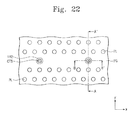
- FIG. 32 is a plan view illustrating an example of interconnection between conductive lines, according to an exemplary embodiment of the inventive concept.
- FIGS. 33 and 35 are sectional views taken along line A-A′ of FIG. 32
- FIGS. 34 and 36 are sectional views taken along line B-B′ of FIG. 32 .
- bit lines BL_a and BL_b are provided to connect the cell pillars to each other.
- the cell pillars PL 1 and PL 2 are grouped into cell groups PLG 1 and PLG 2 separated by the residual insulating layer 111 .
- Each of the cell groups PLG 1 and PLG 2 includes the first cell pillars PL 1 arranged in a first row, extending in the x direction, adjacent to the separation layers 145 and the second cell pillars PL 2 arranged in a second row, extending in the x direction, between the first row and the residual insulating layer 111 .
- the second cell pillars PL 2 are shifted by a predetermined distance in the x direction and thus are located between the first cell pillars PL 1 .
- the cell groups PLG 1 and PLG 2 adjacent to each other have substantially the same arrangement of the cell pillars PL 1 and PL 2 .
- the cell groups PLG 1 and PLG 2 adjacent to each other may be configured to have a mirror-symmetric arrangement of the cell pillars with respect to each other.
- the inventive concepts are not limited to a cell group having the two rows of cell pillars PL 1 and PL 2 , but may include a cell group having three or more rows of cell pillars.
- a contact connection line SC may serve to connect the contact plugs CTS to each other.
- the contact connection line SC and the bit lines BL_a and BL_b may include a metal layer and/or a conductive metal nitride layer.
- the contact connection line SC may be used to apply a predetermined voltage to the substrate 100 through the contact plugs CTS and the first conductive region 101 .
- the contact connection line SC may extend along the extending direction (e.g., the x direction) of the residual insulating layers 111 .
- the contact connection line SC is provided between the bit lines BL_a and BL_b and the contact plugs CTS.
- the contact connection line SC is formed on the contact plugs CTS, connecting the contact plugs CTS to each other.
- the contact connection line SC is further positioned under the bit lines BL_a and BL_b.
- the contact connection line SC may be provided on the bit lines BL_a and BL_b.
- the bit lines BL_a and BL_b cross the separation layers 145 and the residual insulating layers 111 .
- the first bit lines BL_a does not overlap the contact plugs CTS
- the second bit lines BL_b overlaps the contact plugs CTS.
- the first cell pillars PL 1 of the first and second cell groups PLG 1 and PLG 2 may be connected to the same first bit line BL_a through the first bit line contact plugs CP 1 .
- the cell pillars PL_a overlapped with the second bit lines BL_b are not connected to the second bit lines BL_b.
- the second bit lines BL_b is electrically separated from the contact connection line SC by a second interlayered insulating layer 115 .
- the second hit lines BL_b is electrically connected to the contact connection line SC via second hit line plugs CP 2 penetrating the second interlayered insulating layer 115 .
- the second bit lines BL_b may serve to apply a predetermined voltage to the first conductive region 101 .
- FIG. 37 is a plan view illustrating an example of interconnection between conductive lines, according to an exemplary embodiment of the inventive concept.
- FIGS. 38 and 40 are sectional views taken along line A-A′ of FIG. 37
- FIGS. 39 and 41 are sectional views taken along line B-B′ of FIG. 37 .
- the elements and features of this example that are previously shown and described will not be described in much further detail.
- the cell pillars PL_a overlapped with the second bit lines BL_b are connected to the second bit lines BL_b via the third bit line plugs CP 3 .
- the second bit lines BL_b is electrically separated from the contact connection line SC by the second interlayered insulating layer 115 .
- the second bit lines BL_b are electrically connected to the contact connection line SC via the second hit line plugs CP 2 penetrating the second interlayered insulating layer 115 .
- the second bit lines BL_b may serve to apply a predetermined voltage to the substrate 100 .
- the cell pillars PL_a connected to the second bit lines BL_b also apply a predetermined voltage to the substrate 100 .
- FIGS. 42 and 43 are plan views illustrating examples of interconnection between conductive lines, according to an exemplary embodiment of the inventive concept.
- the second bit lines BL_b is connected to the contact plugs CTS via the second bit line plugs CP 2 , without the contact connection line SC.
- the second hit lines BL_b may be electrically connected to each other by an additional conductive line (not shown).
- the cell pillars PL_a overlapped with the second bit lines BL_b are not be connected to the second bit lines BL_b.
- the cell pillars PL_a overlapped with the second bit lines BL_b are connected to the second bit lines BL_b via the third bit line plugs CP 3 .
- the cell pillars PL_a connected to the second bit lines BL_b, along with the contact plugs CTS may serve to apply a predetermined voltage to the substrate 100 .
- FIG. 44 is a plan view illustrating a memory cell region MR and a pad contact region CR, according to an exemplary embodiment of the inventive concept
- FIG. 45 is a sectional view taken along line C-C′ of FIG. 44 .
- the formation of the contact plugs CTS and pad contact plugs PCP will be described with reference to FIGS. 44 and 45 .
- the memory cell region MR is a region having the cell pillars PL.
- the pad contact region CR is a region having the pad contact plugs PCP.
- the pad contact plugs PCP are connected to the horizontal electrodes PG extended from the memory cell region MR to the pad contact region CR.
- the horizontal electrodes PG has an edge having a step-wise structure which allows each of the pad contact plugs PCP to be connected to corresponding horizontal electrodes PG.
- the pad contact plugs PCP are formed in a third interlayered insulating layer 116 and each of them is connected to the corresponding one of the horizontal electrodes PG vertically spaced apart from each other.
- the pad contact plugs PCP may be connected to each other by a global word line GWL.
- a process of forming the contact plug CTS may be at least partially used to form contact plugs in the peripheral circuit region or the pad contact region CR.
- at least one step of the process of forming the contact plug CTS may be applied in forming the pad contact plugs PCP.
- at least one of pad contact holes 124 in which the pad contact plugs PCP will be formed, may be formed during the formation of the contact holes 128 .
- the contact plugs CTS and the pad contact plugs PCP may be simultaneously formed by forming a conductive layer to fill the contact hole 128 and the pad contact holes 124 .
- FIGS. 46 and 47 are sectional views illustrating a process of forming the pad contact region CR and the peripheral circuit region PR, according to an exemplary embodiment of the inventive concept.
- peripheral transistors TR are formed in the peripheral circuit region PR.
- the peripheral transistors TR are formed on active regions defined by device isolation layers IS.
- Each of the peripheral transistors TR includes source/drain regions 104 and a gate electrode GE.
- a fourth interlayered insulating layer 117 is formed on the peripheral circuit region PR to cover the peripheral transistors TR.
- a first layer stack ST 1 is formed on the pad contact region CR.
- the first layer stack ST 1 includes the first insulating layers 120 and the second insulating layers 110 , which are alternately stacked on the substrate 100 .
- the first insulating layers 120 and the second insulating layers 110 are formed to cover the entire top surface of the substrate 100 and then are partially removed from the peripheral circuit region PR to expose the fourth interlayered insulating layer 117 .
- a step-wise structure is formed at the edge of the first layer stack ST 1 in the pad contact region CR.
- a fifth interlayered insulating layer 119 is formed to cover the first layer stack ST 1 with the step-wise structure.
- the fifth interlayered insulating layer 119 may be formed to expose a top surface of the first layer stack ST 1 .
- a second layer stack ST 2 is formed on the first layer stack ST 1 .
- the second layer stack ST 2 covers the pad contact region CR and the peripheral circuit region PR.
- the second layer stack ST 2 includes the first insulating layers 120 and the second insulating layers 110 , which are alternately stacked on the substrate 100 .
- the horizontal electrodes PG having the step-wise structure are formed in the pad contact region CR.
- the second layer stack ST 2 is patterned to form the step-wise structure, and then, the second insulating layers 110 is replaced with a conductive layer, as described with reference to FIGS. 8 and 9 .
- a sixth interlayered insulating layer 118 is formed on the second layer stack ST 2 with the step-wise structure.
- the second layer stack ST 2 formed on the peripheral circuit region PR is protected and remains in the peripheral circuit region PR. Thereafter, peripheral circuit contacts CPL is formed in the peripheral circuit region PR to penetrate the second layer stack ST 2 .
- the peripheral circuit contacts CPL is connected to the source/drain regions 104 and/or the gate electrodes GE of the peripheral transistors TR through the first and second insulating layers 120 and 110 .
- the second insulating layers 110 of the second layer stack ST 2 are provided between the first insulating layers 120 . According to an exemplary embodiment, each of them may be located at substantially the same level as the corresponding one of the horizontal electrodes PG.
- the peripheral circuit contacts CPL are formed to be in contact with the first and second insulating layers 120 and 110 .
- Peripheral conductive lines PD are formed on the second layer stack ST 2 to connect the peripheral circuit contacts CPL with each other.
- inventive concept is not limited to the embodiments described above, but modifications and changes may be made within the scope of the inventive concept defined in the following claims.
- the features and configurations of the afore-described embodiments may be exchanged or combined with each other within the scope of the inventive concept.
- FIG. 48 is a schematic block diagram illustrating an example of memory systems including a semiconductor device according to an exemplary embodiment of the inventive concept.
- an electronic system 1100 includes a controller 1110 , an input/output (I/O) unit 1120 , a memory device 1130 , an interface unit 1140 and a data bus 1150 . At least two of the controller 1110 , the I/O unit 1120 , the memory device 1130 and the interface unit 1140 may communicate with each other through the data bus 1150 .
- the data bus 1150 may correspond to a path through which electrical signals are transmitted.
- the memory device 1130 may include a semiconductor device according to an exemplary embodiment of the inventive concept.
- the controller 1110 may include a microprocessor, a digital signal processor, a microcontroller or a logic device.
- the logic device may have a similar function to any one of the microprocessor, the digital signal processor and the microcontroller.
- the I/O unit 1120 may include a keypad, a keyboard or a display unit.
- the memory device 1130 may store data and/or commands.
- the memory device 1130 may include a semiconductor device according to an exemplary embodiment of the present inventive concept.
- the memory device 1130 may further include a different type of semiconductor devices from the semiconductor device.
- the interface unit 1140 may transmit electrical data to a communication network or may receive electrical data from a communication network.
- the interface unit 1140 may operate in a wireless or cable connection.
- the interface unit 1140 may include an antenna for wireless communication or a transceiver for cable communication.
- the electronic system 1100 may further include a fast DRAM (Dynamic Random Access Memory) device and/or a fast SRAM (Static Random Access Memory) device that acts as an operating memory device for improving an operation of the controller 1110 .
- a fast DRAM Dynamic Random Access Memory
- SRAM Static Random Access Memory
- the electronic system 1100 may be applied to a lap-top computer, a personal digital assistant (PDA), a portable computer, a web tablet, a wireless phone, a mobile phone, a digital music player, a memory card or an electronic product.
- the electronic product may be configured to receive or transmit information data by a wireless communication.
- a memory card 1200 may include a memory device 1210 .
- the memory device 1210 may include a semiconductor device according to an exemplary embodiment of the inventive concept.
- the memory device 1210 may further include a different type of semiconductor devices from the semiconductor device.
- the memory card 1200 includes a memory controller 1220 that controls data communication between a host and the memory device 1210 .
- the memory device 1210 and/or the controller 1220 may include a semiconductor device according to an exemplary embodiment of the inventive concept.
- the memory controller 1220 includes a processing unit 1222 that controls overall operations of the memory card 1200 .
- the memory controller 1220 further includes an SRAM device 1221 used as an operation memory of the processing unit 1222 .
- the memory controller 1220 further includes a host interface unit 1223 and a memory interface unit 1225 .
- the host interface unit 1223 may be configured to include a data communication protocol between the memory card 1200 and the host.
- the memory interface unit 1225 may connect the memory controller 1220 to the memory device 1210 .
- the memory controller 1220 further includes an error check and correction (ECC) block 1224 .
- ECC error check and correction
- the FCC block 1224 may detect and correct errors of data which are read out from the memory device 1210 .
- the memory card 1200 may further include a read only memory (ROM) device that stores code data to interface with a host device.
- ROM read only memory
- the memory card 1200 may be used as a portable data storage card.
- the memory card 1200 may replace hard disks of computer systems as solid state disks (SSD) of the computer systems.
- FIG. 50 is a schematic block diagram illustrating an example of information processing systems including a semiconductor device according to an exemplary embodiment of the inventive concept.
- an information processing system 1300 includes a memory system 1310 including a semiconductor device according to an exemplary embodiment of the inventive concept.
- the information processing system 1300 also includes a modem 1320 a central processing unit (CPU) 1330 , a RAM 1340 , and a user interface 1350 , which may be electrically connected to the memory system 1310 via a system bus 760 .
- the memory system 1310 may be configured to have the same technical features as the memory system of FIG. 48 . Data processed by the CPU 1330 and/or input from the outside may be stored in the memory system 1310 .
- the memory system 1310 may be provided as a solid state drive SSD, and thus, the information processing system 1300 may be able to store reliably a large amount of data in the memory system 1310 . This increase in reliability enables the memory system 1310 to minimize resources for error correction and realize a high speed data exchange function.
- the information processing system 1300 may be also configured to include an application chipset, a camera image processor (CIS), and/or an input/output device.
- a semiconductor device or memory system may be packaged in various kinds of ways.
- the semiconductor device or memory system may be employed in a Package on Package (PoP), Ball Grid Array (BGA), Chip Scale Package (CSP), Plastic Leaded Chip Carrier (PLCC), Plastic Dual In-line Package (PDIP), Die in Waffle Pack, Die in Wafer Form, Chip On Board (COB), Ceramic Dual In-line Package (CERDIP), Plastic Metric Quad Flat Pack (MQFP), Thin Quad Flat Pack (TQFP), Small Outline Integrated Circuit (SOIC), Shrink Small Outline Package (SSOP), Thin Small Outline Package (TSOP), System In Package (SIP), Multi Chip Package (MCP), Wafer-level Fabricated Package (WFP), or Wafer-level Processed Stack Package (WSP).
- PoP Package on Package
- BGA Ball Grid Array
- CSP Chip Scale Package
- PLCC Plastic Leaded Chip Carrier
- PDIP Plastic Dual In-line Package
- COB Chip On Board
- CERDIP Ceramic Dual
- a contact plug structure may be formed without a process of forming an additional insulating layer, which may be used to electrically separate contact plugs from other conductive elements. Accordingly, a contact hole may be formed to have a reduced size, and thus, it may increase an integration density of a semiconductor device.
Abstract
A semiconductor device includes a plurality of first insulating layers and a plurality of second layers alternately and vertically stacked on a substrate. Each of the plurality of second layers includes a horizontal electrode horizontally separated by a second insulating layer. A contact plug penetrates the plurality of first insulating layers and the second insulating layer of the plurality of second layers.
Description
This application is a divisional of U.S. application Ser. No. 13/938,833 filed on Jul. 10, 2013, which claims priority under 35 U.S.C. §119 to Korean Patent Application No. 10-2012-0075595, filed on Jul. 11, 2012, in the Korean Intellectual Property Office, the disclosure of which is incorporated by reference herein in its entirety.
The present inventive concepts relates to a semiconductor device, more particularly, to a vertical-type semiconductor device and a method of manufacturing the same.
To satisfy excellent performance and low cost, semiconductor devices have been highly integrated. A density of integration in memory devices is an important factor in determining the prices of products. In typical Two-Dimensional (2D) memory devices, a density of integration is mainly determined by the occupied area of memory cells, which is affected by the level of fine pattern forming technology. However, this fine pattern forming technology, performed by high-cost equipments, may limit a density of integration in 2D semiconductor memory devices.
To overcome these limitations, three-dimensional (3D) memory devices including memory cells three-dimensionally arranged have been proposed. For mass production of the 3D memory devices, however, a process technology which reduces manufacturing costs per bit relative to 2D memory devices and secures reliable product characteristics is required.
According to an exemplary embodiment of the present inventive concept, a semiconductor device includes a plurality of horizontal electrodes vertically stacked on a substrate. A plurality of first insulating layers each is disposed between a corresponding pair of the plurality of horizontal electrodes. A plurality of second insulating layers each is disposed between a corresponding pair of the plurality of first insulating layers and is disposed at the same vertical level as a corresponding one of the plurality of horizontal electrodes. A contact structure penetrates the first and second insulating layers. The contact structure is in contact with the first insulating layers and the second insulating layers.
According to an exemplary embodiment of the present inventive concept, a semiconductor device includes a stack structure disposed on a substrate. The stack structure includes four or more first insulating layers and four or more second insulating layers sequentially stacked one over the other. A contact structure penetrates the stack structure. Four or more horizontal electrodes are extended between the first insulating layers. The first insulating layers and the second insulating layers are in contact with the contact structure. The first insulating layers include different materials from the second insulating layers.
According to an exemplary embodiment of the present inventive concept, a plurality of first insulating layers and a plurality of second insulating layers are alternately stacked on a substrate. Spaces are formed between the plurality of second insulating layers by partially etching the plurality of second insulating layers. The spaces are defined by the plurality of first insulating layers and remaining portions of the plurality of second insulating layers. Horizontal electrodes are disposed in the spaces. A contact structure penetrates the plurality of first insulating layers and the remaining portions of the plurality of second insulating layers.
According to an exemplary embodiment of the inventive concept, a semiconductor device includes a plurality of first insulating layers and a plurality of second layers alternately and vertically stacked on a substrate. Each of the plurality of second layers includes a horizontal electrode horizontally separated by a second insulating layer. A contact plug penetrates the plurality of first insulating layers and the second insulating layer of the plurality of second layers.
These and other features of the inventive concept will become more apparent by describing in detail exemplary embodiments thereof with reference to the accompanying drawings of which:
Exemplary embodiments of the inventive concepts will be described below in more detail with reference to the accompanying drawings. The inventive concepts may, however, be embodied in different forms and should not be construed as limited to the embodiments set forth herein; rather, these exemplary embodiments are provided so that this disclosure will be thorough and complete, and will fully convey the concept of example embodiments to those of ordinary skill in the art. In the drawings, the thicknesses of layers and regions are exaggerated for clarity. Like reference numerals denote like elements throughout the specification and drawings, and thus their description will be omitted.
It will be understood that when an element is referred to as being “connected” or “coupled” to another element, it may be directly connected or coupled to the other element or intervening elements may be present. In contrast, when an element is referred to as being “directly connected” or “directly coupled” to another element, there are no intervening elements present. As used herein the term “and/or” includes any and all combinations of one or more of the associated listed items. Other words used to describe the relationship between elements or layers should be interpreted in a like fashion (e.g., “between” versus “directly between,” “adjacent” versus “directly adjacent,” “on” versus “directly on”).
It will be understood that, although the terms “first”, “second”, etc. may be used herein to describe various elements, components, regions, layers and/or sections, these elements, components, regions, layers and/or sections should not be limited by these terms. These terms are only used to distinguish one element, component, region, layer or section from another element, component, region, layer or section. Thus, a first element, component, region, layer or section discussed below could be termed a second element, component, region, layer or section without departing from the teachings of example embodiments.
Spatially relative terms, such as “beneath,” “below,” “lower,” “above,” “upper” and the like, may be used herein for ease of description to describe one element or feature's relationship to another element(s) or feature(s) as illustrated in the figures. It will be understood that the spatially relative terms are intended to encompass different orientations of the device in use or operation in addition to the orientation depicted in the figures. For example, if the device in the figures is turned over, elements described as “below” or “beneath” other elements or features would then be oriented “above” the other elements or features. Thus, the exemplary term “below” may encompass both an orientation of above and below. The device may be otherwise oriented (rotated 90 degrees or at other orientations) and the spatially relative descriptors used herein interpreted accordingly.
The terminology used herein is for the purpose of describing particular embodiments only and is not intended to be limiting of example embodiments. As used herein, the singular forms “a,” “an” and “the” are intended to include the plural forms as well, unless the context clearly indicates otherwise. It will be further understood that the terms “comprises”, “comprising”, “includes” and/or “including,” if used herein, specify the presence of stated features, integers, steps, operations, elements and/or components, but do not preclude the presence or addition of one or more other features, integers, steps, operations, elements, components and/or groups thereof.
Example embodiments of the inventive concept are described herein with reference to cross-sectional illustrations that are schematic illustrations of idealized embodiments (and intermediate structures) of exemplary embodiments. As such, variations from the shapes of the illustrations as a result, for example, of manufacturing techniques and/or tolerances, are to be expected. Thus, exemplary embodiments of the inventive concepts should not be construed as limited to the particular shapes of regions illustrated herein but are to include deviations in shapes that result, for example, from manufacturing. For example, an implanted region illustrated as a rectangle may have rounded or curved features and/or a gradient of implant concentration at its edges rather than a binary change from implanted to non-implanted region. Likewise, a buried region formed by implantation may result in some implantation in the region between the buried region and the surface through which the implantation takes place. Thus, the regions illustrated in the figures are schematic in nature and their shapes are not intended to illustrate the actual shape of a region of a device and are not intended to limit the scope of example embodiments.
Unless otherwise defined, all terms (including technical and scientific terms) used herein have the same meaning as commonly understood by one of ordinary skill in the art to which example embodiments of the inventive concepts belong. It will be further understood that terms, such as those defined in commonly-used dictionaries, should be interpreted as having a meaning that is consistent with their meaning in the context of the relevant art and will not be interpreted in an idealized or overly formal sense unless expressly so defined herein.
The memory cell array 10 is connected to the address decoder 20 through a plurality of word lines WL, and be connected to the read/write circuit 30 through a plurality of bit lines BL. The memory cell array 10 includes a plurality of memory cells (not shown). The memory cell array 10 may store one or more bits in each cell.
The address decoder 20 is connected to the memory cell array 10 through the word lines WL. The address decoder 20 operates according to the control of the control logic 50. The address decoder 20 may receive an address ADDR from the outside. The address decoder 20 decodes a row address among the received address ADDR to select a corresponding word line from among the word lines WL. Also, the address decoder 20 decodes a column address among the address ADDR and transfers the decoded column address to the read/write circuit 30. For example, the address decoder 20 may include elements such as a row decoder, a column decoder and an address buffer.
The read/write circuit 30 is connected to the memory cell array 10 through the bit line BL. The read/write circuit 30 may be connected to the data input/output circuit 40 through the data lines DL. The read/write circuit 30 may operate according to the control of the control logic 50. In response to the control, the read/write circuit 30 receives the decoded column address from the address decoder 20, and selects a bit line BL using the decoded column address. For example, the read/write circuit 30 receives data from the data input/output circuit 40 and writes the received data in the memory cell array 10. The read/write circuit 30 reads data from the memory cell array 10 and transfers the read data to the data input/output circuit 40. The read/write circuit 30 reads data from a first storage region (not shown) of the memory cell array 10, and writes the read data in a second storage region (not shown) of the memory cell array 10. For example, the read/write circuit 30 may perform a copy-back operation.
The read/write circuit 30 may include elements which include a page buffer (not shown) or a page register (not shown) and a column selection circuit (not shown). As another example, the read/write circuit 30 may include elements which include a sensing amplifier, a write driver and a column selection circuit.
The data input/output circuit 40 is connected to the read/write circuit 30 through the data lines DL. The data input/output circuit 40 operates according to the control of the control logic 50. The data input/output circuit 40 exchanges data DATA with the outside. For example, the data input/output circuit 40 transfers the data DATA to the read/write circuit 30 through the data lines DL. The data input/output circuit 40 outputs the data DATA, which is transferred from the read/write circuit 30 through the data lines DL, to the outside. For example, the data input/output circuit 40 may include a data buffer (not shown).
The control logic 50 is connected to the address decoder 20, the read/write circuit 30 and the data input/output circuit 40. The control logic 50 controls the operation of a 3D semiconductor device. The control logic 50 operates in response to a control signal CTRL transferred from the outside.
A semiconductor device and a method of fabricating the same, according to an exemplary embodiment of the inventive concept, will be described with reference to FIGS. 3 through 11 . FIG. 3 is a plan view illustrating a semiconductor device according to an exemplary embodiment of the inventive concept. FIGS. 4 through 11 are sectional views taken along lines A-A′ and B-B′ of FIG. 3 .
Referring to FIGS. 3 and 4 , a substrate 100 is provided. The substrate 100 may include a silicon substrate, a germanium substrate, or a silicon-germanium substrate. The substrate 100 may include a doped region having a first conductivity type. For example, the first conductivity type may be a p-type. A first conductive region 101 is provided in the substrate 100. The first conductive region 101 may be configured to apply a specific voltage to the substrate 100. The first conductive region 101 may be a doped region provided in an upper region of the substrate 100. For example, the first conductive region 101 may have the same conductivity type as the substrate 100 and have a doping concentration higher than the substrate 100. For example, the first conductive region 101 may have a line shape extending along an x direction. The first conductive region 101 may be formed by an ion implantation process.
A buffer insulating layer 105 is formed on the substrate 100. The buffer insulating layer 105 may include a silicon oxide layer. The buffer insulating layer 105 may be formed using a thermal oxidation process. Second insulating layers 110 and first insulating layers 120 are alternately stacked on the buffer insulating layer 105. According to an exemplary embodiment, the numbers of the first insulating layers 120 and the second insulating layers 110 may be four or more. For example, a pair of the first and second insulating layers 120 and 110 may be repeatedly formed ten or more times. The second insulating layers 110 and the first insulating layers 120 may include materials having etch selectivity with respect to each other. For example, when a specific etch recipe is used to etch the second insulating layers 110, the first insulating layers 120 may include materials having a much lower etch rate than that of the second insulating layers 110 to the specific etch recipe. The etch selectivity may be quantitatively expressed in terms of a ratio of an etch rate of the second insulating layers 110 to that of the first insulating layers 120. For example, the second insulating layers 110 may include materials having etch selectivity of 1:10 to 1:200 (or 1:30 to 1:100) with respect to the first insulating layers 120. For example, the second insulating layers 110 may include a silicon nitride layer, a silicon oxynitride layer, and/or a polysilicon layer. The first insulating layers 120 may include a silicon oxide layer. The insulating layers 110 and 120 may be formed by a chemical vapor deposition (CVD).
Referring to FIGS. 3 and 5 , cell holes 125 are formed through the insulating layers 110 and 120 to expose the substrate 100 using an anisotropic etching process.
Referring to FIGS. 3 and 6 , a semiconductor layer 130 and a gap-fill insulating layer 140 are sequentially formed to fill each of the cell holes 125. The semiconductor layer 130 may be conformally formed in such a manner that the cell holes 125 are not completely filled with the semiconductor layer 130. For example, the semiconductor layer 130 may be formed to conformally cover sidewalls of the insulating layers 110 and 120 and a top surface of the substrate 100. The sidewalls of the insulating layers 110 and 120 and the top surface of the substrate 100 define the cell holes 125. The gap-fill insulating layer 140 may be formed to fill the cell holes 125 provided with the semiconductor layer 130. The semiconductor layer 130 and the gap-fill insulating layer 140 may cover a top surface of an uppermost one of the first insulating layers 120. Alternatively, the semiconductor layer 130 may fill the cell holes 125. In such a case, the gap-fill insulating layer 140 need not be provided.
For example, the semiconductor layer 130 may include a polysilicon layer having the first conductivity type. The gap-fill insulating layer 140 may include a silicon oxide layer or a silicon oxynitride layer. Alternatively, the semiconductor layer 130 may include a conductive layer (e.g., a doped semiconductor layer, a metal layer, a conductive metal nitride layer, a silicide layer), or a nano structure (e.g., a carbon nanotube or a graphene layer). According to an exemplary embodiment, the semiconductor layer 130 and the gap-fill insulating layer 140 may be formed using a chemical vapor deposition process or an atomic layer deposition (ALD) process.
Referring to FIGS. 3 and 7 , the semiconductor layer 130, separation regions 126 may be formed to expose the substrate 100 through the gap-fill insulating layer 140, and the insulating layers 110 and 120. The separation regions 126 may be delimited by sidewalls of the insulating layers 110 and 120 and the top surface of the substrate 100. For example, the separation regions 126 may be formed to have a trench-shaped structure extending along the x direction.
Referring to FIGS. 3 and 8 , the second insulating layers 110 exposed by the separation regions 126 may be partially removed to form recess regions 144. For example, the recess regions 144 may be empty regions produced by removing the second insulating layers 110. In the case where the second insulating layers 110 include a silicon nitride layer or a silicon oxynitride layer, the formation of the recess regions 144 may be performed using an etching solution containing a phosphoric acid. Each of the recess regions 144 may be formed to partially expose a sidewall of the semiconductor layer 130. For example, portions of the second insulating layers 110 (hereinafter, referred as to residual insulating layers 111) may remain between the first insulating layers 120, even after the formation of the recess regions 144. The residual insulating layers 111 may be formed to be overlapped with the first conductive region 101, in plan view. The formation of the residual insulating layers 111 will be described in more detail with reference to FIGS. 16 through 21 .
Referring to FIGS. 3 and 9 , a memory element 135 and horizontal electrodes PG are formed in the recess regions 144. For example, a memory layer (not shown) and a conductive layer (not shown) may be sequentially formed in the recess regions 144 and in the separation region 126. The memory element 135 and horizontal electrodes PG may be formed by removing portions of the memory layer and the conductive layer located in the separation region 126 or at the outside of the recess regions 144. For example, the memory element 135 may include a tunnel insulating layer (not shown), a charge storing layer (not shown) on the tunnel insulating layer, and a blocking insulating layer (not shown) on the charge storing layer. Alternatively, the memory element 135 may be a variable resistance pattern. The horizontal electrodes PG are vertically spaced apart from each other by the first insulating layers 120. The horizontal electrodes PG may include a doped silicon layer, a metal layer, a metal silicide layer, and/or a conductive metal nitride layer. The memory element 135 and the horizontal electrodes PG will be described in more detail with reference to FIGS. 30A through 30D and FIGS. 31A through 31D .
Referring to FIGS. 3 and 10 , separation layers 145 are formed to fill the separation regions 126. For example, an insulating layer (not shown) may be formed in the separation regions 126 and may be formed on an upper surface of the gap-fill insulating layer 140 of FIG. 9 . For example, the insulating layer may include a silicon oxide layer and/or a silicon oxynitride layer. A planarization process may be performed to remove the insulating layer (now shown), the gap-fill insulating layer 140 of FIG. 9 and the semiconductor layer 130 of FIG. 9 . In such a case, the separation layers 145 are left in the separation regions 126 and the gap-fill insulating layer 140 of FIG. 9 is left in the cell holes 125 to form the separation layers 145 and gap-fill insulating patterns 141, respectively. The gap-fill insulating layer 140 of FIG. 9 is localized in each of the cell holes 125 to form the gap-fill insulating patterns 141.
Second conductive regions 132 are formed on the cell pillars PL. For example, upper portions of the cell pillars PL may be removed, and a doped polysilicon layer or a metal layer may be deposited. For example, the second conductive regions 132 may include a doped pattern of an n-type semiconductor. The second conductive regions 132 may serve as drain regions of the semiconductor device. A first interlayered insulating layer 114 is formed to cover the second conductive regions 132 using a chemical vapor deposition. The first interlayered insulating layer 114 may include a silicon oxide layer and/or a silicon oxynitride layer.
Referring to FIGS. 3 and 11 , a contact plug CTS is formed through the residual insulating layers 111. The contact plug CTS is electrically connected to the first conductive region 101 through the first interlayered insulating layer 114, the first insulating layers 120, and the residual insulating layers 111. In an exemplary embodiment, when a semiconductor device may include contact plugs CTS, the contact plugs CTS may be arranged along a direction in which the residual insulating layers 111 are extended. For example, the contact plugs CTS may be arranged in the x direction. The contact plug CTS is formed in contact hole 128 and is in contact with the first conductive region 101 exposed by the contact hole 128. The contact hole 128 may be formed by using an anisotropic etching process. The contact plug CTS may include a metal layer, a conductive metal nitride layer, a metal silicide layer, and/or a doped semiconductor layer. In the case where the contact plug CTS includes metal, a metal silicide layer may be formed between the contact plug CTS and the first conductive region 101.
A semiconductor device according to an exemplary embodiment of the inventive concept will be described with reference to FIGS. 3 and 11 . The semiconductor includes the horizontal electrodes PG, the cell pillars PL, and contact plugs CTS. The horizontal electrodes PG are sequentially stacked on the substrate 100. The horizontal electrodes PG are horizontally separated from each other by the separation layers 145 and extend along the x direction. The impurity regions 102 are provided in the substrate 100 below the separation layers 145. The impurity regions 102 may include doped regions having a different conductivity type from the substrate 100. The impurity regions 102 may serve as the common source lines of the semiconductor device.
The cell pillars PL are connected to the substrate 100 through the horizontal electrodes PG. In an exemplary embodiment, the cell pillars PL include a first row of cell pillars adjacent to the separation layers 145 and a second row of cell pillars adjacent to the residual insulating layers 111. The memory elements 135 are provided between the cell pillars PL and the horizontal electrodes PG. For example, each of the memory elements 135 may include the tunnel insulating layer, the charge storing layer on the tunnel insulating layer, and the blocking insulating layer on the charge storing layer. Alternatively, each of the memory elements 135 may include a variable resistance pattern.
The horizontal electrodes PG are vertically separated from each other by the first insulating layers 120. The residual insulating layers 111 are provided between the first insulating layers 120. The residual insulating layers 111 are located at the same level as the corresponding one of the horizontal electrodes PG. For example, the horizontal electrodes PG partially fill interlayer regions between the first insulating layers, and the residual insulating layers 111 fill the remaining portions of the interlayer regions. Top and bottom surfaces of the residual insulating layers 111 are in contact with the first insulating layers 120. Each of the residual insulating layers 111 is extended along a direction in which the separation layers 145 are extended. For example, the separation layers 145 may be extended along the x direction. The horizontal electrodes PG may include portions interposed between the cell pillars PL and the residual insulating layers 111. The residual insulating layers 111 may include a material having etch selectivity with respect to the first insulating layers 120. For example, in the case where the first insulating layers 120 include a silicon oxide layer, the residual insulating layers 111 may include a silicon nitride layer, a silicon oxynitride layer, and/or a polysilicon layer.
The contact plug CTS is connected to the first conductive region 101 of the substrate 100 penetrating the first insulating layers 120 and the residual insulating layers 111. The contact plug CTS is in contact with the first insulating layers 120 and the residual insulating layers 111. For example, the first conductive region 101 may include a doped region having the same conductivity type as and having a higher concentration than the substrate 100. The contact plug CTS is electrically separated from the horizontal electrodes PG by the first insulating layers 120 and the residual insulating layers 111. In an exemplary embodiment, when the semiconductor device includes contact plugs CTS, the contact plugs CTS may be arranged along a direction in which the residual insulating layers 111 are extended. For example, the residual insulating layers 111 are extended along the x direction. The contact plugs CTS may be spaced apart at a distance that may be greater than that between the cell pillars PL arranged along the x direction.
The number of memory elements 135 may be increased by stacking more layers on the substrate 100. In such a case, the residual insulating layers 111 surrounding the contact plug CTS may eliminate an additional insulation layer to isolate the contact plug CTS from the horizontal electrodes PG. The additional insulating layer may have a thickness that is necessary to prevent an electrical breakdown of the additional insulation layer, and thus this elimination increases integration density of the vertical-type semiconductor memory cells.
According to an exemplary embodiment of the inventive concept, portions of the second insulating layers 111 remain, and the contact plug CTS penetrates the remaining portions of the second insulating layers 111. This structure of the contact plug CTS enables to omit a process of forming the additional insulating layer to electrically separate the horizontal electrodes PG from the contact plug CTS. For example, a contact structure of the semiconductor device may be fabricated using a simplified process without a process step of forming the additional insulating layer. Furthermore, this omission of the additional insulating layer reduces a size of the contact hole 128 in which the contact plug CTS is provided, and thus, the semiconductor device increases integration density of memory cells.
A semiconductor device according to an exemplary embodiment of the inventive concept will be described with reference to FIGS. 12 and 13 . FIG. 12 is a plan view illustrating semiconductor devices and methods of fabricating the same, according to an exemplary embodiment of the inventive concept. FIG. 13 is a sectional view taken along lines A-A′ and B-B′ of FIG. 12 . The exemplary embodiment of FIGS. 12 and 13 is substantially similar to that of FIGS. 3 to 11 , except for a structure of a contact plug CTS. For the sake of brevity, the elements and features previously shown and described will not be described in much further detail.
A contact plug CTS of FIG. 12 according to an exemplary embodiment is extended along a direction in which the residual insulating layers 111 are extended. For example, the residual insulating layers 111 are extended along the x direction, and are formed in a trench 129 exposing a portion of the substrate 100. For example, the contact plug CTS includes a line-shaped horizontal section extending along the separation layers 145. The first conductive region 101 is extended along the extending direction of the contact plug CTS and is electrically connected to the contact CTS. For example, the trench 129 may be formed using an anisotropic etching process. The trench 129 may be delimited by sidewalls of the residual insulating layers 111, sidewalls of the first insulating layers 120, and the top surface of the substrate 100.
A semiconductor device according to an exemplary embodiment of the inventive concept will be described with reference to FIGS. 14 and 15 . FIG. 14 is a plan view illustrating a semiconductor device and a method of fabricating the same, according to an exemplary embodiment of the inventive concept, and FIG. 15 is a sectional view taken along lines A-A and B-B′ of FIG. 14 . This exemplary embodiment of FIGS. 14 and 15 is substantially similar to that of FIGS. 3 to 11 , except for a shape of the cell pillars PL and a structural relationship between the cell pillars PL and the horizontal electrodes PG. For the sake of brevity, the elements and features of this example previously shown and described will not be described in much further detail.
The cell pillars PL of FIG. 14 are separated from each other by second gap-fill insulating patterns 142 arranged along the x direction. Each of the cell pillars PL has a ‘U’-shaped structure filled with a first gap-fill insulating pattern 141. Each of the first gap-fill insulating patterns 141 has substantially the same width as the corresponding one of the cell pillars PL and is in contact with the second gap-fill insulating patterns 142. For example, trenches 127 may be formed, exposing the substrate 100. A semiconductor layer (not shown) and an insulating layer (not shown) may be formed in the trenches 127 (not shown). Thereafter, the semiconductor layer (not shown) and the insulating layer (not shown) may be divided along the x direction to form the cell pillars PL. The second gap-fill insulating patterns 142 are formed between the cell pillars PL. The second gap-fill insulating patterns 142 may include a silicon oxide layer and/or a silicon ox nitride layer.
According to an exemplary embodiment, the horizontal electrodes PG are separated from the residual insulating layers 111 with the cell pillars PL interposed therebetween. For example, the residual insulating layers 111 and the first insulating layers 120 provided along the sidewall of the contact plug CTS are separated from the horizontal electrodes PG by the cell pillars PL and the second gap-fill insulating patterns 142. The residual insulating layers 111 are in contact with the sidewalls of the cell pillars PL.
Referring to FIG. 18 , in an intermediate stage of the horizontal etching process, the second insulating layers 110 are completely removed from regions between the first sub-dielectric layers RG1 having a width smaller than the second sub-dielectric layers RG2. By contrast, the second insulating layers 110 remain in regions between the second sub-dielectric layers RG2 having a width greater than the first sub-dielectric layer. In a final stage of the horizontal etching process, as shown in FIG. 19 , the sidewall of all the cell pillars PL are completely exposed, and thus, the second insulating layers 110 are removed except the residual insulating layer 111. The residual insulating layers 111 are positioned within a localized region between two arrays of the cell pillars PL. For example, in the case where the first and second sub-dielectric layers RG2 have widths of d1 and d2, respectively, a width d3 of the residual insulating layer 111 is equal to a width of d2−2*d1. For example, the width d2 of the second sub-dielectric layers RG2 may be greater than twice the width d1 of the first sub-dielectric layers RG1.
As shown in FIG. 19 , the residual insulating layer 111 is interposed between a first and a second separation regions 126_a and 126_b. For example, the first separation region 126_a is positioned between the RG1 and RG2 at the left to the residual insulating layer 111, and the second separation region 126_b is positioned between the RG1 and RG2 at the right to the residual insulating layer 111. The residual insulating layer 111 is interposed between the first and second separation regions 126_a and 126_b. If the second insulating layers are etched at the same lateral etch rate from the separation regions 126_a and 126_b, a distance d5 between the first separation region 126_a and the residual insulating layers 111 may be substantially the same with a distance d6 between the second separation region 126_b and the residual insulating layer 111. The width d3 of the residual insulating layers 111 may be greater than a width d4 of the separation regions 126.
Alternatively, the horizontal etching process may be stopped at the stage depicted in FIG. 18 . In this case, the residual insulating layers 111 are penetrated by some of the cell pillars PL, and the subsequent processes described above with reference to FIGS. 9 to 11 are performed thereto.
As shown in FIG. 21 , the cell pillars includes two kinds of arrays including a first array of cell pillars PL1 and a second array of cell pillars PL2. The second array of cell pillars PL2 is shifted by a predetermined distance in the x axis. According to an exemplary embodiment, the first sub-dielectric layers RG1 includes the first and the second cell pillars PL1 and PL2, and the second sub-dielectric layers RG2 includes two first arrays of cell pillars PL1. The two first arrays of cell pillars PL1 are spaced apart from each other by the residual insulating layer 111 interposed therebetween.
As shown in FIG. 21 , the horizontal etching process may be stopped when the second insulating layers 110 disposed between the first sub-dielectric layers RG1 are completely removed. The cell pillars PL penetrating the second sub-dielectric layers RG2 may be exposed. In the case where the first and second sub-dielectric layers RG2 have widths of d1 and d2, the width d3 of the residual insulating layers 111 may equal to a width of d2−d1.
Referring to FIGS. 22 and 23 , the impurity region 102 and the first conductive region 101 are formed in an upper region of the substrate 100. The impurity region 102 is commonly connected to the cell pillars PL spaced apart from each other in both y direction and x direction. The impurity region 102 may be formed using an ion implantation process. In an exemplary embodiment, the impurity region 102 may be formed to have a different conductivity type from that of the substrate 100. The first conductive region 101 is a line-shaped doped region extending along the x direction. In an exemplary embodiment, the first conductive region 101 may include the same conductivity type as that of the substrate 100 and may have an impurity concentration higher than that of the substrate 100.
The buffer insulating layer 105 is formed on the substrate 100 provided with the impurity region 102 and the first conductive region 101. The first insulating layers 120 and the horizontal electrodes PG are alternately stacked on the buffer insulating layer 105. In an exemplary embodiment, each of the horizontal electrodes PG may include a doped semiconductor layer. The memory element 135 is formed in the cell holes 125 penetrating the first insulating layers 120 and the horizontal electrodes PG. The memory element 135 is interposed between sidewalls of the cell holes 125 and the cell pillars PL. The cell pillars PL is connected to the impurity region 102 through the memory element 135. The second conductive regions 132 are formed on the cell pillars PL. The second conductive regions 132 may be formed by partially removing upper portions of the cell pillars PL and depositing a doped polysilicon layer or a metal layer thereon. In an exemplary embodiment, the second conductive regions 132 may include n-type impurities. The first interlayered insulating layer 114 is formed to cover the cell pillars PL.
The contact hole 128 is formed to expose the substrate 100 through the first insulating layers 120 and the horizontal electrodes PG. For example, the contact hole 128 is formed to expose side surfaces of the first insulating layers 120 and the horizontal electrodes PG. The contact hole 128 may be formed by performing an anisotropic etching process. The contacts CTS are formed in the contact holes 128. The contacts CTS are connected to the first conductive regions 101, respectively.
Referring to FIGS. 22 and 24 , second insulating layers 112 are locally formed on the side surfaces of the horizontal electrodes PG exposed by the contact holes 128. The second insulating layers 112 are also formed on the top surface of the substrate 100 exposed by the contact holes 128. In an exemplary embodiment, the second insulating layers 112 may include oxide layers, which may be formed by thermally oxidizing the exposed side surfaces of the horizontal electrodes PG.
Referring to FIGS. 22 and 25 , the contact plugs CTS are formed in the contact holes 128. The contact plugs CTS are connected to the first conductive regions 101, respectively. In an exemplary embodiment, before the formation of the contact plugs CTS, an etching process may be further performed to remove partially the second insulating layers 112 and expose the top surface of the first conductive regions 101.
Each of the second insulating layers 112 are formed to surround the contact plugs CTS. For example, each of the second insulating layers 112 may be shaped like a ring being in contact with the contact plugs CTS. The contact plugs CTS are electrically separated from the horizontal electrodes PG by the second insulating layers 112 and the first insulating layers 120.
Referring to FIGS. 3 and 26 , a first conductive region 103 is formed on the top surface of the substrate 100 exposed by the buffer insulating layer 105 and a mask layer 107. The first conductive region 103 may include a metal layer and/or a metal silicide layer. In an exemplary embodiment, the first conductive region 103 is formed to fill a gap region delimited by the mask layer 107. Alternatively, the first conductive region 103 may be formed by forming and patterning a metal layer and/or a metal silicide layer on the substrate 100. The first conductive region 103 includes a line-shaped structure extending along the x direction.
Referring to FIGS. 3 and 27 , the second insulating layers 110 and the first insulating layers 120 are alternately stacked on the resulting structure provided with the first conductive region 103. In an exemplary embodiment, the mask layer 107 may be removed before the formation of the insulating layers 110 and 120.
The subsequent processes may be performed in the same manner as those described with reference to FIGS. 5 through 11 and thus further detail descriptions will be omitted.
The first conductive region 101 of FIG. 29 may be formed after the formation of the horizontal electrodes PG. For example, as shown in FIGS. 28 and 29 , the first conductive region 101 may be formed by an ion implantation process, which is performed after the formation of the contact hole 128 penetrating the residual insulating layers 111 and the first insulating layers 120. In the case where the number of the contact holes 128 is two or more, the first conductive region 101 may include a plurality of impurity regions separated from each other and may be formed below the plurality of the contact holes 128, respectively.
Referring to FIG. 30A , the memory element 135 includes a blocking insulating layer 135 c formed on the horizontal electrodes PG, a tunnel insulating layer 135 a formed on the cell pillars PL and a charge storing layer 135 b interposed therebetween. The memory element 135 is partially interposed between the horizontal electrodes PG and the first insulating layers 120. The blocking insulating layer 135 c may include a high-k dielectric layer, such as an aluminum oxide layer or a hafnium oxide layer. The blocking insulating layer 135 c may include a multi-layered structure including a plurality of layers. The charge storing layer 135 b may include a charge-trap layer or an insulating layer provided with conductive nano particles. For example, the charge-trap layer may include a silicon nitride layer. The tunnel insulating layer 135 a may include a silicon oxide layer.
Referring to FIGS. 30B through 30D , unlike that shown in FIG. 30A , at least a portion of the memory element 135 is partially interposed between the first insulating layers 120 and the cell pillars PL. Referring to FIG. 30B , the tunnel insulating layer 135 a is extended between the first insulating layers 120 and the cell pillars PL, and the charge storing layer 135 b and the blocking insulating layer 135 c are extended between the first insulating layers 120 and the horizontal electrodes PG. Referring to FIG. 30C , the tunnel insulating layer 135 a and the charge storing layer 135 b are extended between the first insulating layers 120 and the cell pillars PL, and the blocking insulating layer 135 c is extended between the first insulating layers 120 and the horizontal electrodes PG. Referring to FIG. 30D , the tunnel insulating layer 135 a, the charge storing layer 135 b, and the blocking insulating layer 135 c are extended between the first insulating layers 120 and the cell pillars PL.
The cell pillars PL may include a conductive material. For example, the cell pillars PL may include a doped semiconductor layer, a metal layer, a conductive metal nitride layer, a silicide layer, and/or a nano structure (e.g., carbon nanotube or graphene). In an exemplary embodiment, the memory element 135 may include a variable resistance pattern. The variable resistance pattern may include materials having a variable resistance property. Referring to FIG. 31A , the memory element 135 is formed and localized between the horizontal electrodes PG and the cell pillars PL. Referring to FIG. 31B , the memory element 135 is extended between the first insulating layers 120 and the cell pillars PL and is further extended between the horizontal electrodes PG and the cell pillars PL. Referring to FIG. 31C , the memory element 135 is formed between the horizontal electrodes PG and the cell pillars PL and is further extended between the first insulating layers 120 and the horizontal electrodes PG.
The memory element 135 may include a material (for example, a phase-changeable material), whose electric resistance may be changed according to thermal energy applied thereto. Thermal energy may be generated by an electric current passing through an electrode adjacent to the memory element 135. The phase-changeable material may include antimony (Sb), tellurium (Te), and/or selenium (Se). For example, the phase-changeable material may have the properties of chalcogenide glasses. The material may include tellurium (Te) having about 20 to about 80 atomic percent concentration, antimony (Sb) having about 5 to about 50 atomic percent concentration, and germanium (Ge) having the remaining concentration. In addition, the phase-changeable material may further include impurities such as N, O, C, Bi, In, B, Sn, Si, Ti, Al, Ni, Fe, Dy, and/or La. In an exemplary embodiment, the memory element 135 may include GeBiTe, InSb, GeSb, and/or Ga Sb.
The memory element 135 may be configured to have a layered structure whose electric resistance may be changed according to a spin transferring phenomenon of an electric current flowing through the memory element 135. For example, the memory element 135 may be configured to have a layered structure exhibiting a magneto-resistance property and may include at least one ferromagnetic material and/or at least one antiferromagnetic material.
The memory element 135 may include perovskite compounds or transition metal oxides. For example, the memory element 135 may include niobium oxide, titanium oxide, nickel oxide, zirconium oxide, vanadium oxide, PCMO((Pr,Ca)MnO3), strontium-titanium oxide, barium-strontium-titanium oxide, strontium-zirconium oxide, barium-zirconium oxide, and/or barium-strontium-zirconium oxide.
Referring to FIG. 31D , a switching element SW is interposed between the memory element 135 and the horizontal electrodes PG. The switching element SW may include a material exhibiting a self-rectifying property or a nonlinear current-voltage property. For example, the switching element SW may be configured to form a pn-junction diode.
Referring to FIGS. 32 through 36 , bit lines BL_a and BL_b are provided to connect the cell pillars to each other. The cell pillars PL1 and PL2 are grouped into cell groups PLG1 and PLG2 separated by the residual insulating layer 111. Each of the cell groups PLG1 and PLG2 includes the first cell pillars PL1 arranged in a first row, extending in the x direction, adjacent to the separation layers 145 and the second cell pillars PL2 arranged in a second row, extending in the x direction, between the first row and the residual insulating layer 111. Along the x direction, the second cell pillars PL2 are shifted by a predetermined distance in the x direction and thus are located between the first cell pillars PL1. The cell groups PLG1 and PLG2 adjacent to each other have substantially the same arrangement of the cell pillars PL1 and PL2. Alternatively, the cell groups PLG1 and PLG2 adjacent to each other may be configured to have a mirror-symmetric arrangement of the cell pillars with respect to each other. The inventive concepts are not limited to a cell group having the two rows of cell pillars PL1 and PL2, but may include a cell group having three or more rows of cell pillars.
A contact connection line SC may serve to connect the contact plugs CTS to each other. The contact connection line SC and the bit lines BL_a and BL_b may include a metal layer and/or a conductive metal nitride layer. The contact connection line SC may be used to apply a predetermined voltage to the substrate 100 through the contact plugs CTS and the first conductive region 101. The contact connection line SC may extend along the extending direction (e.g., the x direction) of the residual insulating layers 111. In an exemplary embodiment, the contact connection line SC is provided between the bit lines BL_a and BL_b and the contact plugs CTS. For example, the contact connection line SC is formed on the contact plugs CTS, connecting the contact plugs CTS to each other. The contact connection line SC is further positioned under the bit lines BL_a and BL_b. Alternatively, the contact connection line SC may be provided on the bit lines BL_a and BL_b.
The bit lines BL_a and BL_b cross the separation layers 145 and the residual insulating layers 111. In an exemplary embodiments, the first bit lines BL_a does not overlap the contact plugs CTS, and the second bit lines BL_b overlaps the contact plugs CTS. The first cell pillars PL1 of the first and second cell groups PLG1 and PLG2 may be connected to the same first bit line BL_a through the first bit line contact plugs CP1.
The cell pillars PL_a overlapped with the second bit lines BL_b are not connected to the second bit lines BL_b. In an exemplary embodiment, as shown in FIGS. 33 and 34 , the second bit lines BL_b is electrically separated from the contact connection line SC by a second interlayered insulating layer 115. Alternatively, as shown in FIGS. 35 and 36 , the second hit lines BL_b is electrically connected to the contact connection line SC via second hit line plugs CP2 penetrating the second interlayered insulating layer 115. In this case, the second bit lines BL_b may serve to apply a predetermined voltage to the first conductive region 101.
According to an exemplary embodiment, the cell pillars PL_a overlapped with the second bit lines BL_b are connected to the second bit lines BL_b via the third bit line plugs CP3. In an exemplary embodiment, as shown in FIGS. 38 and 39 , the second bit lines BL_b is electrically separated from the contact connection line SC by the second interlayered insulating layer 115. Alternatively, as shown in FIGS. 40 and 41 , the second bit lines BL_b are electrically connected to the contact connection line SC via the second hit line plugs CP2 penetrating the second interlayered insulating layer 115. In this case, the second bit lines BL_b may serve to apply a predetermined voltage to the substrate 100. In addition to the contact plugs CTS, the cell pillars PL_a connected to the second bit lines BL_b also apply a predetermined voltage to the substrate 100.
The formation of the contact plugs CTS and pad contact plugs PCP will be described with reference to FIGS. 44 and 45 . The memory cell region MR is a region having the cell pillars PL. The pad contact region CR is a region having the pad contact plugs PCP. The pad contact plugs PCP are connected to the horizontal electrodes PG extended from the memory cell region MR to the pad contact region CR. In the pad contact region CR, the horizontal electrodes PG has an edge having a step-wise structure which allows each of the pad contact plugs PCP to be connected to corresponding horizontal electrodes PG. The pad contact plugs PCP are formed in a third interlayered insulating layer 116 and each of them is connected to the corresponding one of the horizontal electrodes PG vertically spaced apart from each other. In the case where the two or more pad contact plugs PCP are connected to one of the horizontal electrodes PG, the pad contact plugs PCP may be connected to each other by a global word line GWL.
A process of forming the contact plug CTS may be at least partially used to form contact plugs in the peripheral circuit region or the pad contact region CR. In an exemplary embodiment, at least one step of the process of forming the contact plug CTS may be applied in forming the pad contact plugs PCP. For example, at least one of pad contact holes 124, in which the pad contact plugs PCP will be formed, may be formed during the formation of the contact holes 128. The contact plugs CTS and the pad contact plugs PCP may be simultaneously formed by forming a conductive layer to fill the contact hole 128 and the pad contact holes 124.
Referring to FIG. 46 , peripheral transistors TR are formed in the peripheral circuit region PR. The peripheral transistors TR are formed on active regions defined by device isolation layers IS. Each of the peripheral transistors TR includes source/drain regions 104 and a gate electrode GE. A fourth interlayered insulating layer 117 is formed on the peripheral circuit region PR to cover the peripheral transistors TR.
A first layer stack ST1 is formed on the pad contact region CR. The first layer stack ST1 includes the first insulating layers 120 and the second insulating layers 110, which are alternately stacked on the substrate 100. In forming the first layer stack ST1, the first insulating layers 120 and the second insulating layers 110 are formed to cover the entire top surface of the substrate 100 and then are partially removed from the peripheral circuit region PR to expose the fourth interlayered insulating layer 117. In removing the first and the second insulating layers 120 and 110, a step-wise structure is formed at the edge of the first layer stack ST1 in the pad contact region CR. Thereafter, a fifth interlayered insulating layer 119 is formed to cover the first layer stack ST1 with the step-wise structure. The fifth interlayered insulating layer 119 may be formed to expose a top surface of the first layer stack ST1.
A second layer stack ST2 is formed on the first layer stack ST1. The second layer stack ST2 covers the pad contact region CR and the peripheral circuit region PR. The second layer stack ST2 includes the first insulating layers 120 and the second insulating layers 110, which are alternately stacked on the substrate 100.
Referring to FIG. 47 , the horizontal electrodes PG having the step-wise structure are formed in the pad contact region CR. In forming the horizontal electrodes PG having the step-wise structure, the second layer stack ST2 is patterned to form the step-wise structure, and then, the second insulating layers 110 is replaced with a conductive layer, as described with reference to FIGS. 8 and 9 . In an exemplary embodiment, a sixth interlayered insulating layer 118 is formed on the second layer stack ST2 with the step-wise structure.
In exemplary embodiment, in forming the horizontal electrodes PG with the step-wise structure, the second layer stack ST2 formed on the peripheral circuit region PR is protected and remains in the peripheral circuit region PR. Thereafter, peripheral circuit contacts CPL is formed in the peripheral circuit region PR to penetrate the second layer stack ST2. The peripheral circuit contacts CPL is connected to the source/drain regions 104 and/or the gate electrodes GE of the peripheral transistors TR through the first and second insulating layers 120 and 110. The second insulating layers 110 of the second layer stack ST2 are provided between the first insulating layers 120. According to an exemplary embodiment, each of them may be located at substantially the same level as the corresponding one of the horizontal electrodes PG. The peripheral circuit contacts CPL are formed to be in contact with the first and second insulating layers 120 and 110. Peripheral conductive lines PD are formed on the second layer stack ST2 to connect the peripheral circuit contacts CPL with each other.
The inventive concept is not limited to the embodiments described above, but modifications and changes may be made within the scope of the inventive concept defined in the following claims. For example, the features and configurations of the afore-described embodiments may be exchanged or combined with each other within the scope of the inventive concept.
Referring to FIG. 48 , an electronic system 1100 according to an exemplary embodiment of the inventive concept includes a controller 1110, an input/output (I/O) unit 1120, a memory device 1130, an interface unit 1140 and a data bus 1150. At least two of the controller 1110, the I/O unit 1120, the memory device 1130 and the interface unit 1140 may communicate with each other through the data bus 1150. The data bus 1150 may correspond to a path through which electrical signals are transmitted. The memory device 1130 may include a semiconductor device according to an exemplary embodiment of the inventive concept.
The controller 1110 may include a microprocessor, a digital signal processor, a microcontroller or a logic device. The logic device may have a similar function to any one of the microprocessor, the digital signal processor and the microcontroller. The I/O unit 1120 may include a keypad, a keyboard or a display unit. The memory device 1130 may store data and/or commands. The memory device 1130 may include a semiconductor device according to an exemplary embodiment of the present inventive concept. The memory device 1130 may further include a different type of semiconductor devices from the semiconductor device. The interface unit 1140 may transmit electrical data to a communication network or may receive electrical data from a communication network. The interface unit 1140 may operate in a wireless or cable connection. For example, the interface unit 1140 may include an antenna for wireless communication or a transceiver for cable communication. Although not shown in the drawings, the electronic system 1100 may further include a fast DRAM (Dynamic Random Access Memory) device and/or a fast SRAM (Static Random Access Memory) device that acts as an operating memory device for improving an operation of the controller 1110.
The electronic system 1100 may be applied to a lap-top computer, a personal digital assistant (PDA), a portable computer, a web tablet, a wireless phone, a mobile phone, a digital music player, a memory card or an electronic product. The electronic product may be configured to receive or transmit information data by a wireless communication.
Referring to FIG. 49 , a memory card 1200 may include a memory device 1210. In an exemplary embodiment, the memory device 1210 may include a semiconductor device according to an exemplary embodiment of the inventive concept. The memory device 1210 may further include a different type of semiconductor devices from the semiconductor device. The memory card 1200 includes a memory controller 1220 that controls data communication between a host and the memory device 1210. The memory device 1210 and/or the controller 1220 may include a semiconductor device according to an exemplary embodiment of the inventive concept.
The memory controller 1220 includes a processing unit 1222 that controls overall operations of the memory card 1200. The memory controller 1220 further includes an SRAM device 1221 used as an operation memory of the processing unit 1222. The memory controller 1220 further includes a host interface unit 1223 and a memory interface unit 1225. The host interface unit 1223 may be configured to include a data communication protocol between the memory card 1200 and the host. The memory interface unit 1225 may connect the memory controller 1220 to the memory device 1210. The memory controller 1220 further includes an error check and correction (ECC) block 1224. The FCC block 1224 may detect and correct errors of data which are read out from the memory device 1210. Although not shown in the drawings, the memory card 1200 may further include a read only memory (ROM) device that stores code data to interface with a host device. The memory card 1200 may be used as a portable data storage card. Alternatively, the memory card 1200 may replace hard disks of computer systems as solid state disks (SSD) of the computer systems.
Referring to FIG. 50 , an information processing system 1300 includes a memory system 1310 including a semiconductor device according to an exemplary embodiment of the inventive concept. The information processing system 1300 also includes a modem 1320 a central processing unit (CPU) 1330, a RAM 1340, and a user interface 1350, which may be electrically connected to the memory system 1310 via a system bus 760. The memory system 1310 may be configured to have the same technical features as the memory system of FIG. 48 . Data processed by the CPU 1330 and/or input from the outside may be stored in the memory system 1310. Here, the memory system 1310 may be provided as a solid state drive SSD, and thus, the information processing system 1300 may be able to store reliably a large amount of data in the memory system 1310. This increase in reliability enables the memory system 1310 to minimize resources for error correction and realize a high speed data exchange function. Although not shown in the drawing, it will be apparent to those of ordinary skill in the art that the information processing system 1300 may be also configured to include an application chipset, a camera image processor (CIS), and/or an input/output device.
Furthermore, a semiconductor device or memory system according to an exemplary embodiment of the inventive concept may be packaged in various kinds of ways. For example, the semiconductor device or memory system may be employed in a Package on Package (PoP), Ball Grid Array (BGA), Chip Scale Package (CSP), Plastic Leaded Chip Carrier (PLCC), Plastic Dual In-line Package (PDIP), Die in Waffle Pack, Die in Wafer Form, Chip On Board (COB), Ceramic Dual In-line Package (CERDIP), Plastic Metric Quad Flat Pack (MQFP), Thin Quad Flat Pack (TQFP), Small Outline Integrated Circuit (SOIC), Shrink Small Outline Package (SSOP), Thin Small Outline Package (TSOP), System In Package (SIP), Multi Chip Package (MCP), Wafer-level Fabricated Package (WFP), or Wafer-level Processed Stack Package (WSP).
According to exemplary embodiments of the inventive concept, a contact plug structure may be formed without a process of forming an additional insulating layer, which may be used to electrically separate contact plugs from other conductive elements. Accordingly, a contact hole may be formed to have a reduced size, and thus, it may increase an integration density of a semiconductor device.
While the present inventive concept has been shown and described with reference to exemplary embodiments thereof, it will be apparent to those of ordinary skill in the art that various changes in form and detail may be made therein without departing from the sprit and scope of the inventive concept as defined by the following claims.
Claims (19)
1. A method of fabricating a semiconductor device, comprising:
alternately stacking a plurality of first insulating layers and a plurality of second insulating layers on a substrate, each of the plurality of second insulating layers being a single layer which has a different material from each of the plurality of first insulating layers;
forming spaces between the plurality of first insulating layers by partially etching the plurality of second insulating layers, wherein the spaces are defined by the plurality of first insulating layers and remaining portions of the plurality of second insulating layers;
forming a plurality of horizontal electrodes in the spaces; and
forming a contact structure penetrating the plurality of first insulating layers and the remaining portions of the plurality of second insulating layers,
wherein after the forming of the spaces, the forming of the contact structure is performed, and
wherein the remaining portions of the second insulating layers are interposed between the contact structure and the plurality of horizontal electrodes.
2. The method of claim 1 ,
wherein the contact structure is in contact with the plurality of first insulating layers and the remaining portions of the plurality of second insulating layers.
3. The method of claim 1 , further comprising:
forming a first conductive region in the substrate, wherein the contact structure is connected to the first conductive region.
4. The method of claim 3 ,
wherein the forming of the first conductive region is performed before the forming of the plurality of first and second insulating layers, and the first conductive region has a substantially same conductivity type impurity as the substrate and an impurity concentration of the first conductive region is greater than that of the substrate.
5. The method of claim 3 ,
wherein the forming of the first conductive region comprises forming at least one of a metal layer, a metal silicide layer, or a conductive metal nitride layer on the substrate, before the forming of the first and second insulating layers.
6. The method of claim 1 ,
wherein the forming the spaces between the plurality of first insulating layers further comprises:
forming a separation region to penetrate the plurality of first insulating layers and the plurality of second insulating layers,
wherein the separation region exposes a sidewall of the plurality of first insulating layers and second insulating layers; and
wherein the partial etching of the plurality of second insulating layers selectively recesses the plurality of second insulating layers through the separation region.
7. The method of claim 6 ,
wherein the separation region horizontally divides the plurality of first insulating layers into a plurality of first sub-insulating layers and a plurality of second sub-insulating layers, and a width of the plurality of first sub-insulating layers is greater than that of the plurality of second sub-insulating layers, and
wherein the partial etching of the plurality of second insulating layers removes the plurality of second insulating layers except in a localized region between the first sub-insulating layers.
8. The method of claim 1 , further comprising:
forming a cell pillar connected to the substrate and penetrating the first insulating layers and the second insulating layers; and
forming a plurality of memory elements between the cell pillar and the plurality of horizontal electrodes,
wherein the forming of the spaces between the plurality of first insulating layers is performed after the forming of the cell pillars.
9. The method of claim 1 , further comprising:
forming a plurality of pad contact plugs connected to end-portions of the plurality of horizontal electrodes, wherein the forming the contact structure and the forming the plurality of pad contact plugs includes at least one process step simultaneously performed.
10. The method of claim 9 ,
wherein the at least one process step includes an etching process for forming a contact hole for the contact structure and forming pad contact holes for the pad contact plugs.
11. A method of fabricating a semiconductor device, comprising:
alternately stacking a plurality of first insulating layers and a plurality of second insulating layers on a substrate, each of the plurality of second insulating layers being a single layer which has a different material from each of the plurality of first insulating layers;
forming spaces between the plurality of first insulating layers by partially etching the plurality of second insulating layers, wherein the spaces are defined by the plurality of first insulating layers and remaining portions of the plurality of second insulating layers;
forming a plurality of horizontal electrodes in the spaces; and
forming a contact structure penetrating the plurality of first insulating layers and the remaining portions of the plurality of second insulating layers,
wherein after the forming of the spaces, the forming of the contact structure is performed, and
wherein the contact structure is in contact with the plurality of first insulating layers and the remaining portions of the plurality of second insulating layers.
12. The method of claim 11 , further comprising:
forming a first conductive region in the substrate, wherein the contact structure is connected to the first conductive region.
13. The method of claim 12 ,
wherein the forming of the first conductive region is performed before the forming of the plurality of first and second insulating layers, and the first conductive region has a substantially same conductivity type impurity as the substrate and an impurity concentration of the first conductive region is greater than that of the substrate.
14. The method of claim 12 ,
wherein the forming of the first conductive region comprises forming at least one of a metal layer, a metal silicide layer, or a conductive metal nitride layer on the substrate, before the forming of the first and second insulating layers.
15. The method of claim 11 ,
wherein the forming the spaces between the plurality of first insulating layers further comprises:
forming a separation region to penetrate the plurality of first insulating layers and the plurality of second insulating layers,
wherein the separation region exposes a sidewall of the plurality of first insulating layers and second insulating layers; and
wherein the partial etching of the plurality of second insulating layers selectively recesses the plurality of second insulating layers through the separation region.
16. The method of claim 15 ,
wherein the separation region horizontally divides the plurality of first insulating layers into a plurality of first sub-insulating layers and a plurality of second sub-insulating layers, and a width of the plurality of first sub-insulating layers is greater than that of the plurality of second sub-insulating layers, and
wherein the partial etching of the plurality of second insulating layers removes the plurality of second insulating layers except in a localized region between the first sub-insulating layers.
17. The method of claim 11 , further comprising:
forming a cell pillar connected to the substrate and penetrating the first insulating layers and the second insulating layers; and
forming a plurality of memory elements between the cell pillar and the plurality of horizontal electrodes,
wherein the forming of the spaces between the plurality of first insulating layers is performed after the forming of the cell pillars.
18. The method of claim 11 , further comprising:
forming a plurality of pad contact plugs connected to end-portions of the plurality of horizontal electrodes, wherein the forming the contact structure and the forming the plurality of pad contact plugs includes at least one process step simultaneously performed.
19. The method of claim 18 ,
wherein the at least one process step includes an etching process for forming a contact hole for the contact structure and forming pad contact holes for the pad contact plugs.
Priority Applications (2)
| Application Number | Priority Date | Filing Date | Title |
|---|---|---|---|
| US14/563,432 US9698155B2 (en) | 2012-07-11 | 2014-12-08 | Semiconductor devices and methods of fabricating the same |
| US15/609,578 US10903227B2 (en) | 2012-07-11 | 2017-05-31 | Semiconductor devices and methods of fabricating the same |
Applications Claiming Priority (4)
| Application Number | Priority Date | Filing Date | Title |
|---|---|---|---|
| KR10-2012-0075595 | 2012-07-11 | ||
| KR1020120075595A KR101989514B1 (en) | 2012-07-11 | 2012-07-11 | Semiconductor device and method of forming the same |
| US13/938,833 US8946665B2 (en) | 2012-07-11 | 2013-07-10 | Semiconductor devices and methods of fabricating the same |
| US14/563,432 US9698155B2 (en) | 2012-07-11 | 2014-12-08 | Semiconductor devices and methods of fabricating the same |
Related Parent Applications (1)
| Application Number | Title | Priority Date | Filing Date |
|---|---|---|---|
| US13/938,833 Division US8946665B2 (en) | 2012-07-11 | 2013-07-10 | Semiconductor devices and methods of fabricating the same |
Related Child Applications (1)
| Application Number | Title | Priority Date | Filing Date |
|---|---|---|---|
| US15/609,578 Continuation US10903227B2 (en) | 2012-07-11 | 2017-05-31 | Semiconductor devices and methods of fabricating the same |
Publications (2)
| Publication Number | Publication Date |
|---|---|
| US20150093865A1 US20150093865A1 (en) | 2015-04-02 |
| US9698155B2 true US9698155B2 (en) | 2017-07-04 |
Family
ID=49913173
Family Applications (3)
| Application Number | Title | Priority Date | Filing Date |
|---|---|---|---|
| US13/938,833 Active US8946665B2 (en) | 2012-07-11 | 2013-07-10 | Semiconductor devices and methods of fabricating the same |
| US14/563,432 Active US9698155B2 (en) | 2012-07-11 | 2014-12-08 | Semiconductor devices and methods of fabricating the same |
| US15/609,578 Active 2034-12-03 US10903227B2 (en) | 2012-07-11 | 2017-05-31 | Semiconductor devices and methods of fabricating the same |
Family Applications Before (1)
| Application Number | Title | Priority Date | Filing Date |
|---|---|---|---|
| US13/938,833 Active US8946665B2 (en) | 2012-07-11 | 2013-07-10 | Semiconductor devices and methods of fabricating the same |
Family Applications After (1)
| Application Number | Title | Priority Date | Filing Date |
|---|---|---|---|
| US15/609,578 Active 2034-12-03 US10903227B2 (en) | 2012-07-11 | 2017-05-31 | Semiconductor devices and methods of fabricating the same |
Country Status (4)
| Country | Link |
|---|---|
| US (3) | US8946665B2 (en) |
| JP (1) | JP2014022729A (en) |
| KR (1) | KR101989514B1 (en) |
| CN (2) | CN103545276B (en) |
Cited By (4)
| Publication number | Priority date | Publication date | Assignee | Title |
|---|---|---|---|---|
| US11133327B2 (en) | 2018-09-11 | 2021-09-28 | Samsung Electronics Co., Ltd. | Three-dimensional semiconductor device |
| US20220102370A1 (en) * | 2020-09-29 | 2022-03-31 | Samsung Electronics Co., Ltd. | Memory device |
| US11456335B2 (en) | 2020-03-20 | 2022-09-27 | Samsung Electronics Co., Ltd. | Vertical memory devices |
| US20220367648A1 (en) * | 2021-05-13 | 2022-11-17 | Taiwan Semiconductor Manufacturing Company, Ltd. | Method of selective film deposition and semiconductor feature made by the method |
Families Citing this family (120)
| Publication number | Priority date | Publication date | Assignee | Title |
|---|---|---|---|---|
| KR101989514B1 (en) * | 2012-07-11 | 2019-06-14 | 삼성전자주식회사 | Semiconductor device and method of forming the same |
| US9132436B2 (en) | 2012-09-21 | 2015-09-15 | Applied Materials, Inc. | Chemical control features in wafer process equipment |
| KR102035279B1 (en) * | 2013-02-04 | 2019-10-22 | 삼성전자주식회사 | Semiconductor memory device and method of forming the same |
| US10256079B2 (en) | 2013-02-08 | 2019-04-09 | Applied Materials, Inc. | Semiconductor processing systems having multiple plasma configurations |
| US9362130B2 (en) | 2013-03-01 | 2016-06-07 | Applied Materials, Inc. | Enhanced etching processes using remote plasma sources |
| US9230987B2 (en) * | 2014-02-20 | 2016-01-05 | Sandisk Technologies Inc. | Multilevel memory stack structure and methods of manufacturing the same |
| KR102082321B1 (en) * | 2013-08-13 | 2020-02-27 | 삼성전자주식회사 | Semiconductor device and method of manufacturing the same |
| JP2017010951A (en) * | 2014-01-10 | 2017-01-12 | 株式会社東芝 | Semiconductor memory and its manufacturing method |
| JP6129772B2 (en) * | 2014-03-14 | 2017-05-17 | 株式会社東芝 | Semiconductor device and manufacturing method of semiconductor device |
| US9309598B2 (en) | 2014-05-28 | 2016-04-12 | Applied Materials, Inc. | Oxide and metal removal |
| US9773803B2 (en) | 2014-09-08 | 2017-09-26 | Toshiba Memory Corporation | Non-volatile memory device and method of manufacturing same |
| US9455267B2 (en) * | 2014-09-19 | 2016-09-27 | Sandisk Technologies Llc | Three dimensional NAND device having nonlinear control gate electrodes and method of making thereof |
| US9966240B2 (en) | 2014-10-14 | 2018-05-08 | Applied Materials, Inc. | Systems and methods for internal surface conditioning assessment in plasma processing equipment |
| US9355922B2 (en) | 2014-10-14 | 2016-05-31 | Applied Materials, Inc. | Systems and methods for internal surface conditioning in plasma processing equipment |
| KR102217241B1 (en) * | 2014-11-06 | 2021-02-18 | 삼성전자주식회사 | Vertical memory devices and methods of manufacturing the same |
| US11637002B2 (en) | 2014-11-26 | 2023-04-25 | Applied Materials, Inc. | Methods and systems to enhance process uniformity |
| US10573496B2 (en) | 2014-12-09 | 2020-02-25 | Applied Materials, Inc. | Direct outlet toroidal plasma source |
| KR102282138B1 (en) * | 2014-12-09 | 2021-07-27 | 삼성전자주식회사 | Semiconductor device |
| US20160225652A1 (en) | 2015-02-03 | 2016-08-04 | Applied Materials, Inc. | Low temperature chuck for plasma processing systems |
| US9728437B2 (en) | 2015-02-03 | 2017-08-08 | Applied Materials, Inc. | High temperature chuck for plasma processing systems |
| US9419058B1 (en) * | 2015-02-05 | 2016-08-16 | Sandisk Technologies Llc | Memory device with comb-shaped electrode having a plurality of electrode fingers and method of making thereof |
| US9812461B2 (en) * | 2015-03-17 | 2017-11-07 | Sandisk Technologies Llc | Honeycomb cell structure three-dimensional non-volatile memory device |
| KR102309566B1 (en) * | 2015-03-20 | 2021-10-07 | 에스케이하이닉스 주식회사 | Semiconductor device |
| KR102461178B1 (en) * | 2015-03-31 | 2022-11-02 | 삼성전자주식회사 | Semiconductor memory device and method for manufacturing the same |
| JP6504989B2 (en) * | 2015-05-14 | 2019-04-24 | 東京エレクトロン株式会社 | Etching method |
| TWI611560B (en) | 2015-07-06 | 2018-01-11 | Toshiba Memory Corp | Semiconductor memory device and method of manufacturing same |
| TWI582962B (en) * | 2015-07-06 | 2017-05-11 | Toshiba Kk | Semiconductor memory device and manufacturing method thereof |
| US9691645B2 (en) | 2015-08-06 | 2017-06-27 | Applied Materials, Inc. | Bolted wafer chuck thermal management systems and methods for wafer processing systems |
| US9741593B2 (en) | 2015-08-06 | 2017-08-22 | Applied Materials, Inc. | Thermal management systems and methods for wafer processing systems |
| US9349605B1 (en) | 2015-08-07 | 2016-05-24 | Applied Materials, Inc. | Oxide etch selectivity systems and methods |
| US9679906B2 (en) * | 2015-08-11 | 2017-06-13 | Sandisk Technologies Llc | Three-dimensional memory devices containing memory block bridges |
| US10504700B2 (en) | 2015-08-27 | 2019-12-10 | Applied Materials, Inc. | Plasma etching systems and methods with secondary plasma injection |
| US10147736B2 (en) | 2015-09-03 | 2018-12-04 | Toshiba Memory Corporation | Semiconductor memory device and method for manufacturing same |
| US9666597B2 (en) | 2015-09-10 | 2017-05-30 | Kabushiki Kaisha Toshiba | Semiconductor memory device |
| US9704920B2 (en) | 2015-10-27 | 2017-07-11 | Sandisk Technologies Llc | Resistive random access memory containing a steering element and a tunneling dielectric element |
| US9978769B2 (en) | 2015-11-20 | 2018-05-22 | Toshiba Memory Corporation | Semiconductor device |
| US9859363B2 (en) * | 2016-02-16 | 2018-01-02 | Sandisk Technologies Llc | Self-aligned isolation dielectric structures for a three-dimensional memory device |
| US9704801B1 (en) | 2016-02-17 | 2017-07-11 | Kabushiki Kaisha Toshiba | Semiconductor memory device |
| US9941209B2 (en) * | 2016-03-11 | 2018-04-10 | Micron Technology, Inc. | Conductive structures, systems and devices including conductive structures and related methods |
| US9966385B2 (en) | 2016-03-14 | 2018-05-08 | Toshiba Memory Corporation | Semiconductor memory device |
| KR102610403B1 (en) * | 2016-05-04 | 2023-12-06 | 에스케이하이닉스 주식회사 | Three dimensional semiconductor memory device and method for the same |
| US10522371B2 (en) | 2016-05-19 | 2019-12-31 | Applied Materials, Inc. | Systems and methods for improved semiconductor etching and component protection |
| US10504754B2 (en) | 2016-05-19 | 2019-12-10 | Applied Materials, Inc. | Systems and methods for improved semiconductor etching and component protection |
| US9876030B1 (en) | 2016-08-24 | 2018-01-23 | Toshiba Memory Corporation | Semiconductor device and method for manufacturing same |
| US10629473B2 (en) | 2016-09-09 | 2020-04-21 | Applied Materials, Inc. | Footing removal for nitride spacer |
| US10546729B2 (en) | 2016-10-04 | 2020-01-28 | Applied Materials, Inc. | Dual-channel showerhead with improved profile |
| US9934942B1 (en) | 2016-10-04 | 2018-04-03 | Applied Materials, Inc. | Chamber with flow-through source |
| US10163696B2 (en) | 2016-11-11 | 2018-12-25 | Applied Materials, Inc. | Selective cobalt removal for bottom up gapfill |
| US10026621B2 (en) | 2016-11-14 | 2018-07-17 | Applied Materials, Inc. | SiN spacer profile patterning |
| US9972641B1 (en) * | 2016-11-17 | 2018-05-15 | Sandisk Technologies Llc | Three-dimensional memory device having a multilevel drain select gate electrode and method of making thereof |
| US10083982B2 (en) * | 2016-11-17 | 2018-09-25 | Sandisk Technologies Llc | Three-dimensional memory device having select gate electrode that is thicker than word lines and method of making thereof |
| US10566206B2 (en) | 2016-12-27 | 2020-02-18 | Applied Materials, Inc. | Systems and methods for anisotropic material breakthrough |
| US10431429B2 (en) | 2017-02-03 | 2019-10-01 | Applied Materials, Inc. | Systems and methods for radial and azimuthal control of plasma uniformity |
| US10319739B2 (en) * | 2017-02-08 | 2019-06-11 | Applied Materials, Inc. | Accommodating imperfectly aligned memory holes |
| IT201700019392A1 (en) * | 2017-02-21 | 2018-08-21 | Sabrina Barbato | 3D MEMORY DEVICE |
| KR102346409B1 (en) | 2017-03-08 | 2021-12-31 | 양쯔 메모리 테크놀로지스 씨오., 엘티디. | Through-array contact structure of 3D memory device |
| US10943834B2 (en) | 2017-03-13 | 2021-03-09 | Applied Materials, Inc. | Replacement contact process |
| US11276590B2 (en) | 2017-05-17 | 2022-03-15 | Applied Materials, Inc. | Multi-zone semiconductor substrate supports |
| US11276559B2 (en) | 2017-05-17 | 2022-03-15 | Applied Materials, Inc. | Semiconductor processing chamber for multiple precursor flow |
| US10497579B2 (en) | 2017-05-31 | 2019-12-03 | Applied Materials, Inc. | Water-free etching methods |
| KR102385564B1 (en) * | 2017-06-13 | 2022-04-12 | 삼성전자주식회사 | Semiconductor device |
| KR20180135642A (en) * | 2017-06-13 | 2018-12-21 | 삼성전자주식회사 | Vertical type memory device |
| US10920320B2 (en) | 2017-06-16 | 2021-02-16 | Applied Materials, Inc. | Plasma health determination in semiconductor substrate processing reactors |
| US10541246B2 (en) | 2017-06-26 | 2020-01-21 | Applied Materials, Inc. | 3D flash memory cells which discourage cross-cell electrical tunneling |
| US10727080B2 (en) | 2017-07-07 | 2020-07-28 | Applied Materials, Inc. | Tantalum-containing material removal |
| US10541184B2 (en) | 2017-07-11 | 2020-01-21 | Applied Materials, Inc. | Optical emission spectroscopic techniques for monitoring etching |
| KR102307057B1 (en) * | 2017-07-27 | 2021-10-01 | 삼성전자주식회사 | Vertical-type memory device |
| US10043674B1 (en) | 2017-08-04 | 2018-08-07 | Applied Materials, Inc. | Germanium etching systems and methods |
| US10297458B2 (en) | 2017-08-07 | 2019-05-21 | Applied Materials, Inc. | Process window widening using coated parts in plasma etch processes |
| US10361216B2 (en) | 2017-09-20 | 2019-07-23 | Micron Technology, Inc. | Methods used in forming an array of elevationally-extending transistors |
| JP2019067825A (en) | 2017-09-28 | 2019-04-25 | 東芝メモリ株式会社 | Semiconductor device |
| US10903054B2 (en) | 2017-12-19 | 2021-01-26 | Applied Materials, Inc. | Multi-zone gas distribution systems and methods |
| US11328909B2 (en) | 2017-12-22 | 2022-05-10 | Applied Materials, Inc. | Chamber conditioning and removal processes |
| US10236301B1 (en) * | 2017-12-27 | 2019-03-19 | Micron Technology, Inc. | Methods of forming an array of elevationally-extending strings of memory cells |
| US10854426B2 (en) | 2018-01-08 | 2020-12-01 | Applied Materials, Inc. | Metal recess for semiconductor structures |
| US10679870B2 (en) | 2018-02-15 | 2020-06-09 | Applied Materials, Inc. | Semiconductor processing chamber multistage mixing apparatus |
| US10964512B2 (en) | 2018-02-15 | 2021-03-30 | Applied Materials, Inc. | Semiconductor processing chamber multistage mixing apparatus and methods |
| TWI766433B (en) | 2018-02-28 | 2022-06-01 | 美商應用材料股份有限公司 | Systems and methods to form airgaps |
| US10593560B2 (en) | 2018-03-01 | 2020-03-17 | Applied Materials, Inc. | Magnetic induction plasma source for semiconductor processes and equipment |
| US10319600B1 (en) | 2018-03-12 | 2019-06-11 | Applied Materials, Inc. | Thermal silicon etch |
| US10497573B2 (en) | 2018-03-13 | 2019-12-03 | Applied Materials, Inc. | Selective atomic layer etching of semiconductor materials |
| JP2019161010A (en) | 2018-03-13 | 2019-09-19 | 東芝メモリ株式会社 | Semiconductor device |
| US10573527B2 (en) | 2018-04-06 | 2020-02-25 | Applied Materials, Inc. | Gas-phase selective etching systems and methods |
| US10490406B2 (en) | 2018-04-10 | 2019-11-26 | Appled Materials, Inc. | Systems and methods for material breakthrough |
| US10699879B2 (en) | 2018-04-17 | 2020-06-30 | Applied Materials, Inc. | Two piece electrode assembly with gap for plasma control |
| US10886137B2 (en) | 2018-04-30 | 2021-01-05 | Applied Materials, Inc. | Selective nitride removal |
| US10388665B1 (en) | 2018-05-30 | 2019-08-20 | Micron Technology, Inc. | Methods of forming an array of elevationally-extending strings of memory cells having a stack comprising vertically-alternating insulative tiers and wordline tiers and horizontally-elongated trenches in the stack |
| US10411022B1 (en) | 2018-06-14 | 2019-09-10 | Taiwan Semiconductor Manufacturing Co., Ltd. | SRAM structure |
| US10755941B2 (en) | 2018-07-06 | 2020-08-25 | Applied Materials, Inc. | Self-limiting selective etching systems and methods |
| US10872778B2 (en) | 2018-07-06 | 2020-12-22 | Applied Materials, Inc. | Systems and methods utilizing solid-phase etchants |
| CN110729305A (en) * | 2018-07-17 | 2020-01-24 | 旺宏电子股份有限公司 | Memory element and method for manufacturing the same |
| US10672642B2 (en) | 2018-07-24 | 2020-06-02 | Applied Materials, Inc. | Systems and methods for pedestal configuration |
| US10971432B2 (en) * | 2018-08-06 | 2021-04-06 | Samsung Electronics Co., Ltd. | Semiconductor device including a through wiring area |
| WO2020029115A1 (en) * | 2018-08-08 | 2020-02-13 | Yangtze Memory Technologies Co., Ltd. | Memory device and forming method thereof |
| US10892198B2 (en) | 2018-09-14 | 2021-01-12 | Applied Materials, Inc. | Systems and methods for improved performance in semiconductor processing |
| US11049755B2 (en) | 2018-09-14 | 2021-06-29 | Applied Materials, Inc. | Semiconductor substrate supports with embedded RF shield |
| US11062887B2 (en) | 2018-09-17 | 2021-07-13 | Applied Materials, Inc. | High temperature RF heater pedestals |
| KR102627897B1 (en) * | 2018-09-18 | 2024-01-23 | 에스케이하이닉스 주식회사 | Semiconductor device and manufacturing method thereof |
| US11417534B2 (en) | 2018-09-21 | 2022-08-16 | Applied Materials, Inc. | Selective material removal |
| US10593730B1 (en) | 2018-10-10 | 2020-03-17 | Micron Technology, Inc. | Three-dimensional memory array |
| US11682560B2 (en) | 2018-10-11 | 2023-06-20 | Applied Materials, Inc. | Systems and methods for hafnium-containing film removal |
| US10658380B2 (en) * | 2018-10-15 | 2020-05-19 | Micron Technology, Inc. | Formation of termination structures in stacked memory arrays |
| US11121002B2 (en) | 2018-10-24 | 2021-09-14 | Applied Materials, Inc. | Systems and methods for etching metals and metal derivatives |
| WO2020103081A1 (en) * | 2018-11-22 | 2020-05-28 | Yangtze Memory Technologies Co., Ltd. | Three-dimensional memory devices and fabrication methods thereof |
| US11437242B2 (en) | 2018-11-27 | 2022-09-06 | Applied Materials, Inc. | Selective removal of silicon-containing materials |
| CN109686740B (en) * | 2018-11-27 | 2021-05-11 | 长江存储科技有限责任公司 | 3D memory device and method of manufacturing the same |
| CN113206101B (en) * | 2018-11-27 | 2022-07-29 | 长江存储科技有限责任公司 | 3D memory device and method of manufacturing the same |
| US11721527B2 (en) | 2019-01-07 | 2023-08-08 | Applied Materials, Inc. | Processing chamber mixing systems |
| US10920319B2 (en) | 2019-01-11 | 2021-02-16 | Applied Materials, Inc. | Ceramic showerheads with conductive electrodes |
| KR20210076967A (en) * | 2019-01-18 | 2021-06-24 | 양쯔 메모리 테크놀로지스 씨오., 엘티디. | Source contact structure of 3D memory device and manufacturing method thereof |
| JP2020141094A (en) | 2019-03-01 | 2020-09-03 | キオクシア株式会社 | Semiconductor memory device |
| US10930658B2 (en) | 2019-06-24 | 2021-02-23 | Micron Technology, Inc. | Memory arrays and methods used in forming a memory array |
| US11527549B2 (en) * | 2019-10-04 | 2022-12-13 | SK Hynix Inc. | Memory device and method of manufacturing the same |
| US11152388B2 (en) | 2019-10-15 | 2021-10-19 | Micron Technology, Inc. | Memory arrays and methods used in forming a memory array comprising strings of memory cells |
| US11335694B2 (en) | 2019-12-03 | 2022-05-17 | Micron Technology, Inc. | Memory arrays and methods used in forming a memory array comprising strings of memory cells |
| US11276701B2 (en) | 2020-02-11 | 2022-03-15 | Micron Technology, Inc. | Memory arrays comprising strings of memory cells and methods used in forming a memory array comprising strings of memory cells |
| JP2021136270A (en) * | 2020-02-25 | 2021-09-13 | キオクシア株式会社 | Semiconductor storage device and method for manufacturing the same |
| US11545430B2 (en) | 2020-08-28 | 2023-01-03 | Micron Technology, Inc. | Integrated circuitry and method used in forming a memory array comprising strings of memory cells |
| CN112197802A (en) * | 2020-09-27 | 2021-01-08 | 深圳市微秒控制技术有限公司 | Communication fault processing method for absolute value encoder |
| US11380707B2 (en) | 2020-12-09 | 2022-07-05 | Sandisk Technologies Llc | Three-dimensional memory device including backside trench support structures and methods of forming the same |
Citations (31)
| Publication number | Priority date | Publication date | Assignee | Title |
|---|---|---|---|---|
| JP2007317874A (en) | 2006-05-25 | 2007-12-06 | Toshiba Corp | Non-volatile semiconductor storage device |
| US20080061352A1 (en) | 2004-07-29 | 2008-03-13 | Samsung Electronics Co., Ltd. | Semiconductor device and method of manufacturing the same |
| US20080265235A1 (en) | 2007-04-27 | 2008-10-30 | Takeshi Kamigaichi | Nonvolatile semiconductor memory device and manufacturing method thereof |
| KR20090047614A (en) | 2007-11-08 | 2009-05-13 | 삼성전자주식회사 | Vertical type semiconductor device and method of manufacturing the same |
| US20090230462A1 (en) | 2008-03-17 | 2009-09-17 | Kabushiki Kaisha Toshiba | Non-volatile semiconductor storage device and method of manufacturing the same |
| US20090267135A1 (en) | 2008-04-28 | 2009-10-29 | Kabushiki Kaisha Toshiba | Non-volatile semiconductor storage device and method of manufacturing the same |
| US20100034028A1 (en) | 2008-08-06 | 2010-02-11 | Kabushiki Kaisha Toshiba | Method for driving nonvolatile semiconductor memory device |
| US20100090286A1 (en) | 2008-10-09 | 2010-04-15 | Seung-Jun Lee | Vertical-type semiconductor device and method of manufacturing the same |
| US20100133598A1 (en) | 2008-12-03 | 2010-06-03 | Samsung Electronics Co., Ltd. | Nonvolatile memory device and method for fabricating the same |
| US20100133599A1 (en) * | 2008-12-03 | 2010-06-03 | Samsung Electronics Co., Ltd. | Nonvolatile memory device and method for fabricating the same |
| JP2010165794A (en) | 2009-01-14 | 2010-07-29 | Toshiba Corp | Semiconductor memory device |
| CN101794789A (en) | 2009-02-02 | 2010-08-04 | 三星电子株式会社 | Three dimensional memory device |
| US20100258860A1 (en) | 2009-04-10 | 2010-10-14 | Dong-Hyun Kim | Semiconductor device including protrusion type isolation layer |
| US20110013454A1 (en) | 2009-07-15 | 2011-01-20 | Kabushiki Kaisha Toshiba | Nonvolatile semiconductor memory device |
| US20110115010A1 (en) | 2009-11-17 | 2011-05-19 | Sunil Shim | Three-dimensional semiconductor memory device |
| US20110121403A1 (en) | 2008-10-09 | 2011-05-26 | Seung-Jun Lee | Semiconductor device and method of fabricating the same |
| CN102104034A (en) | 2009-12-18 | 2011-06-22 | 三星电子株式会社 | Three-dimensional semiconductor device |
| US20110151667A1 (en) | 2009-12-18 | 2011-06-23 | Sung-Min Hwang | Methods of Manufacturing Three-Dimensional Semiconductor Devices and Related Devices |
| CN102122661A (en) | 2009-12-16 | 2011-07-13 | 三星电子株式会社 | Semiconductor devices and methods for fabricating the same |
| US20110180866A1 (en) | 2010-01-25 | 2011-07-28 | Kabushiki Kaisha Toshiba | Nonvolatile semiconductor memory device and method for manufacturing same |
| US20110216597A1 (en) | 2010-03-03 | 2011-09-08 | Kabushiki Kaisha Toshiba | Nonvolatile semiconductor memory device |
| US20110215394A1 (en) | 2010-03-05 | 2011-09-08 | Kabushiki Kaisha Toshiba | Semiconductor memory device and method for manufacturing same |
| CN102194826A (en) | 2010-03-03 | 2011-09-21 | 三星电子株式会社 | Three-dimensional semiconductor storing device and formation method thereof |
| JP2011199131A (en) | 2010-03-23 | 2011-10-06 | Toshiba Corp | Nonvolatile semiconductor memory device and method of manufacturing the same |
| US20110266604A1 (en) | 2010-04-30 | 2011-11-03 | Kim Suk-Goo | Nonvolatile memory device and method for fabricating the same |
| US8084809B2 (en) | 2008-03-26 | 2011-12-27 | Kabushiki Kaisha Toshiba | Nonvolatile semiconductor memory device including pillars buried inside through holes |
| US20120068241A1 (en) | 2010-09-21 | 2012-03-22 | Kiwamu Sakuma | Nonvolatile semiconductor memory device and method of manufacturing the same |
| US20120070944A1 (en) | 2010-09-17 | 2012-03-22 | Hyu-Jung Kim | Methods of Manufacturing Three Dimensional Semiconductor Devices |
| CN102468321A (en) | 2010-11-10 | 2012-05-23 | 三星电子株式会社 | Non-volatile memory devices having resistance changeable elements and related systems and methods |
| US20120156848A1 (en) * | 2010-12-17 | 2012-06-21 | Sang-Ryol Yang | Method of manufacturing non-volatile memory device and contact plugs of semiconductor device |
| US20120248525A1 (en) | 2011-03-29 | 2012-10-04 | Sunghae Lee | Three dimensional semiconductor memory devices and methods of fabricating the same |
Family Cites Families (12)
| Publication number | Priority date | Publication date | Assignee | Title |
|---|---|---|---|---|
| KR101100142B1 (en) * | 2007-02-21 | 2011-12-29 | 후지쯔 세미컨덕터 가부시키가이샤 | Semiconductor device and process for producing the same |
| JP2009016400A (en) * | 2007-06-29 | 2009-01-22 | Toshiba Corp | Multilayer wiring structure and manufacturing method thereof, and semiconductor device and manufacturing method thereof |
| KR101056385B1 (en) | 2008-10-07 | 2011-08-12 | 한국전자통신연구원 | Detection element |
| JP2011204856A (en) * | 2010-03-25 | 2011-10-13 | Toshiba Corp | Nonvolatile semiconductor memory device, and method of manufacturing the same |
| US20110286804A1 (en) | 2010-05-24 | 2011-11-24 | Peter Lovie | System and Method for Secure Offshore Storage of Crude Oil |
| KR101660432B1 (en) * | 2010-06-07 | 2016-09-27 | 삼성전자 주식회사 | Semiconductor memory device having vertical structure |
| US8803214B2 (en) * | 2010-06-28 | 2014-08-12 | Micron Technology, Inc. | Three dimensional memory and methods of forming the same |
| KR101796630B1 (en) | 2010-09-17 | 2017-11-10 | 삼성전자주식회사 | Three Dimensional Semiconductor Memory Device |
| KR101812260B1 (en) * | 2010-10-20 | 2017-12-28 | 삼성전자주식회사 | Therr dimensional semiconductor memory devices and methods of fabricating the same |
| US20120168858A1 (en) * | 2010-12-30 | 2012-07-05 | Hynix Semiconductor Inc. | Non-volatile memory device and method of fabricating the same |
| KR20120092483A (en) * | 2011-02-11 | 2012-08-21 | 삼성전자주식회사 | Three dimensional semiconductor memory device and method of forming the same |
| KR101989514B1 (en) | 2012-07-11 | 2019-06-14 | 삼성전자주식회사 | Semiconductor device and method of forming the same |
-
2012
- 2012-07-11 KR KR1020120075595A patent/KR101989514B1/en active IP Right Grant
-
2013
- 2013-07-10 JP JP2013144430A patent/JP2014022729A/en active Pending
- 2013-07-10 US US13/938,833 patent/US8946665B2/en active Active
- 2013-07-11 CN CN201310289922.4A patent/CN103545276B/en active Active
- 2013-07-11 CN CN201710151188.3A patent/CN106887404B/en active Active
-
2014
- 2014-12-08 US US14/563,432 patent/US9698155B2/en active Active
-
2017
- 2017-05-31 US US15/609,578 patent/US10903227B2/en active Active
Patent Citations (40)
| Publication number | Priority date | Publication date | Assignee | Title |
|---|---|---|---|---|
| US20080061352A1 (en) | 2004-07-29 | 2008-03-13 | Samsung Electronics Co., Ltd. | Semiconductor device and method of manufacturing the same |
| JP2007317874A (en) | 2006-05-25 | 2007-12-06 | Toshiba Corp | Non-volatile semiconductor storage device |
| US20080265235A1 (en) | 2007-04-27 | 2008-10-30 | Takeshi Kamigaichi | Nonvolatile semiconductor memory device and manufacturing method thereof |
| KR20090047614A (en) | 2007-11-08 | 2009-05-13 | 삼성전자주식회사 | Vertical type semiconductor device and method of manufacturing the same |
| US7679133B2 (en) | 2007-11-08 | 2010-03-16 | Samsung Electronics Co., Ltd. | Vertical-type non-volatile memory devices |
| US20090230462A1 (en) | 2008-03-17 | 2009-09-17 | Kabushiki Kaisha Toshiba | Non-volatile semiconductor storage device and method of manufacturing the same |
| US8084809B2 (en) | 2008-03-26 | 2011-12-27 | Kabushiki Kaisha Toshiba | Nonvolatile semiconductor memory device including pillars buried inside through holes |
| US20090267135A1 (en) | 2008-04-28 | 2009-10-29 | Kabushiki Kaisha Toshiba | Non-volatile semiconductor storage device and method of manufacturing the same |
| US20100034028A1 (en) | 2008-08-06 | 2010-02-11 | Kabushiki Kaisha Toshiba | Method for driving nonvolatile semiconductor memory device |
| US20100090286A1 (en) | 2008-10-09 | 2010-04-15 | Seung-Jun Lee | Vertical-type semiconductor device and method of manufacturing the same |
| US20110121403A1 (en) | 2008-10-09 | 2011-05-26 | Seung-Jun Lee | Semiconductor device and method of fabricating the same |
| US20100133599A1 (en) * | 2008-12-03 | 2010-06-03 | Samsung Electronics Co., Ltd. | Nonvolatile memory device and method for fabricating the same |
| US20100133598A1 (en) | 2008-12-03 | 2010-06-03 | Samsung Electronics Co., Ltd. | Nonvolatile memory device and method for fabricating the same |
| JP2010165794A (en) | 2009-01-14 | 2010-07-29 | Toshiba Corp | Semiconductor memory device |
| CN101794789A (en) | 2009-02-02 | 2010-08-04 | 三星电子株式会社 | Three dimensional memory device |
| US20100193861A1 (en) | 2009-02-02 | 2010-08-05 | Sunil Shim | Three-Dimensional Memory Device |
| US20100258860A1 (en) | 2009-04-10 | 2010-10-14 | Dong-Hyun Kim | Semiconductor device including protrusion type isolation layer |
| US20110013454A1 (en) | 2009-07-15 | 2011-01-20 | Kabushiki Kaisha Toshiba | Nonvolatile semiconductor memory device |
| US20110115010A1 (en) | 2009-11-17 | 2011-05-19 | Sunil Shim | Three-dimensional semiconductor memory device |
| CN102122661A (en) | 2009-12-16 | 2011-07-13 | 三星电子株式会社 | Semiconductor devices and methods for fabricating the same |
| US8482049B2 (en) | 2009-12-16 | 2013-07-09 | Samsung Electronics Co., Ltd. | Semiconductor devices and methods for fabricating the same |
| US8394716B2 (en) | 2009-12-18 | 2013-03-12 | Samsung Electronics Co., Ltd. | Methods of manufacturing three-dimensional semiconductor devices and related devices |
| US20110151667A1 (en) | 2009-12-18 | 2011-06-23 | Sung-Min Hwang | Methods of Manufacturing Three-Dimensional Semiconductor Devices and Related Devices |
| CN102104034A (en) | 2009-12-18 | 2011-06-22 | 三星电子株式会社 | Three-dimensional semiconductor device |
| US8742466B2 (en) | 2009-12-18 | 2014-06-03 | Samsung Electronics Co., Ltd. | Three-dimensional semiconductor device including a mold structure providing gap regions and an interconnection structure including a plurality of interconnection patterns formed in the gap regions |
| US20110180866A1 (en) | 2010-01-25 | 2011-07-28 | Kabushiki Kaisha Toshiba | Nonvolatile semiconductor memory device and method for manufacturing same |
| US20110216597A1 (en) | 2010-03-03 | 2011-09-08 | Kabushiki Kaisha Toshiba | Nonvolatile semiconductor memory device |
| CN102194826A (en) | 2010-03-03 | 2011-09-21 | 三星电子株式会社 | Three-dimensional semiconductor storing device and formation method thereof |
| US20110248327A1 (en) | 2010-03-03 | 2011-10-13 | Yong-Hoon Son | Three-Dimensional Semiconductor Memory Devices and Methods of Forming the Same |
| US9356033B2 (en) | 2010-03-03 | 2016-05-31 | Samsung Electronics Co., Ltd. | Three-dimensional semiconductor memory devices and methods of forming the same |
| US20110215394A1 (en) | 2010-03-05 | 2011-09-08 | Kabushiki Kaisha Toshiba | Semiconductor memory device and method for manufacturing same |
| JP2011199131A (en) | 2010-03-23 | 2011-10-06 | Toshiba Corp | Nonvolatile semiconductor memory device and method of manufacturing the same |
| US20120068253A1 (en) | 2010-03-23 | 2012-03-22 | Kabushiki Kaisha Toshiba | Nonvolatile semiconductor memory device and method for manufacturing the same |
| US20110266604A1 (en) | 2010-04-30 | 2011-11-03 | Kim Suk-Goo | Nonvolatile memory device and method for fabricating the same |
| US20120070944A1 (en) | 2010-09-17 | 2012-03-22 | Hyu-Jung Kim | Methods of Manufacturing Three Dimensional Semiconductor Devices |
| US20120068241A1 (en) | 2010-09-21 | 2012-03-22 | Kiwamu Sakuma | Nonvolatile semiconductor memory device and method of manufacturing the same |
| CN102468321A (en) | 2010-11-10 | 2012-05-23 | 三星电子株式会社 | Non-volatile memory devices having resistance changeable elements and related systems and methods |
| US8664633B2 (en) | 2010-11-10 | 2014-03-04 | Samsung Electronics Co., Ltd. | Non-volatile memory devices having resistance changeable elements and related systems and methods |
| US20120156848A1 (en) * | 2010-12-17 | 2012-06-21 | Sang-Ryol Yang | Method of manufacturing non-volatile memory device and contact plugs of semiconductor device |
| US20120248525A1 (en) | 2011-03-29 | 2012-10-04 | Sunghae Lee | Three dimensional semiconductor memory devices and methods of fabricating the same |
Cited By (6)
| Publication number | Priority date | Publication date | Assignee | Title |
|---|---|---|---|---|
| US11133327B2 (en) | 2018-09-11 | 2021-09-28 | Samsung Electronics Co., Ltd. | Three-dimensional semiconductor device |
| US11456335B2 (en) | 2020-03-20 | 2022-09-27 | Samsung Electronics Co., Ltd. | Vertical memory devices |
| US20220102370A1 (en) * | 2020-09-29 | 2022-03-31 | Samsung Electronics Co., Ltd. | Memory device |
| US11805655B2 (en) * | 2020-09-29 | 2023-10-31 | Samsung Electronics Co., Ltd. | Memory device |
| US20220367648A1 (en) * | 2021-05-13 | 2022-11-17 | Taiwan Semiconductor Manufacturing Company, Ltd. | Method of selective film deposition and semiconductor feature made by the method |
| US11652148B2 (en) * | 2021-05-13 | 2023-05-16 | Taiwan Semiconductor Manufacturing Company, Ltd. | Method of selective film deposition and semiconductor feature made by the method |
Also Published As
| Publication number | Publication date |
|---|---|
| KR101989514B1 (en) | 2019-06-14 |
| US10903227B2 (en) | 2021-01-26 |
| CN103545276B (en) | 2017-04-12 |
| US20170263643A1 (en) | 2017-09-14 |
| JP2014022729A (en) | 2014-02-03 |
| CN106887404A (en) | 2017-06-23 |
| US20150093865A1 (en) | 2015-04-02 |
| KR20140008704A (en) | 2014-01-22 |
| US8946665B2 (en) | 2015-02-03 |
| US20140014889A1 (en) | 2014-01-16 |
| CN103545276A (en) | 2014-01-29 |
| CN106887404B (en) | 2021-07-13 |
Similar Documents
| Publication | Publication Date | Title |
|---|---|---|
| US10903227B2 (en) | Semiconductor devices and methods of fabricating the same | |
| US20230127052A1 (en) | Semiconductor device, systems and methods of manufacture | |
| US9917094B2 (en) | Semiconductor device having staggered pillars | |
| US9466613B2 (en) | Vertical type memory device | |
| US9905574B2 (en) | Three-dimensional semiconductor memory devices | |
| US9515086B2 (en) | Semiconductor device, electronic device, and method of fabricating the same | |
| US8822971B2 (en) | Semiconductor memory device having three-dimensionally arranged resistive memory cells | |
| US8264018B2 (en) | Semiconductor memory device | |
| US8809943B2 (en) | Three dimensional semiconductor memory devices and methods of fabricating the same | |
| US8735860B2 (en) | Variable resistance memory device and method of fabricating the same | |
| US9287167B2 (en) | Vertical type memory device | |
| KR20150002947A (en) | Semiconductor device | |
| KR20110078504A (en) | Semiconductor memory devices and methods of forming the same |
Legal Events
| Date | Code | Title | Description |
|---|---|---|---|
| STCF | Information on status: patent grant |
Free format text: PATENTED CASE |
|
| MAFP | Maintenance fee payment |
Free format text: PAYMENT OF MAINTENANCE FEE, 4TH YEAR, LARGE ENTITY (ORIGINAL EVENT CODE: M1551); ENTITY STATUS OF PATENT OWNER: LARGE ENTITY Year of fee payment: 4 |