US9698092B2 - Electronic device - Google Patents
Electronic device Download PDFInfo
- Publication number
- US9698092B2 US9698092B2 US14/757,968 US201514757968A US9698092B2 US 9698092 B2 US9698092 B2 US 9698092B2 US 201514757968 A US201514757968 A US 201514757968A US 9698092 B2 US9698092 B2 US 9698092B2
- Authority
- US
- United States
- Prior art keywords
- recessed portion
- substrate
- element arrangement
- arrangement recessed
- main
- Prior art date
- Legal status (The legal status is an assumption and is not a legal conclusion. Google has not performed a legal analysis and makes no representation as to the accuracy of the status listed.)
- Expired - Fee Related
Links
Images


Classifications
-
- H—ELECTRICITY
- H01—ELECTRIC ELEMENTS
- H01L—SEMICONDUCTOR DEVICES NOT COVERED BY CLASS H10
- H01L23/00—Details of semiconductor or other solid state devices
- H01L23/48—Arrangements for conducting electric current to or from the solid state body in operation, e.g. leads, terminal arrangements ; Selection of materials therefor
- H01L23/488—Arrangements for conducting electric current to or from the solid state body in operation, e.g. leads, terminal arrangements ; Selection of materials therefor consisting of soldered or bonded constructions
- H01L23/498—Leads, i.e. metallisations or lead-frames on insulating substrates, e.g. chip carriers
- H01L23/49827—Via connections through the substrates, e.g. pins going through the substrate, coaxial cables
-
- H10W70/635—
-
- H—ELECTRICITY
- H01—ELECTRIC ELEMENTS
- H01L—SEMICONDUCTOR DEVICES NOT COVERED BY CLASS H10
- H01L21/00—Processes or apparatus adapted for the manufacture or treatment of semiconductor or solid state devices or of parts thereof
- H01L21/02—Manufacture or treatment of semiconductor devices or of parts thereof
- H01L21/04—Manufacture or treatment of semiconductor devices or of parts thereof the devices having potential barriers, e.g. a PN junction, depletion layer or carrier concentration layer
- H01L21/48—Manufacture or treatment of parts, e.g. containers, prior to assembly of the devices, using processes not provided for in a single one of the groups H01L21/18 - H01L21/326 or H10D48/04 - H10D48/07
- H01L21/4814—Conductive parts
- H01L21/4846—Leads on or in insulating or insulated substrates, e.g. metallisation
- H01L21/486—Via connections through the substrate with or without pins
-
- H—ELECTRICITY
- H01—ELECTRIC ELEMENTS
- H01L—SEMICONDUCTOR DEVICES NOT COVERED BY CLASS H10
- H01L23/00—Details of semiconductor or other solid state devices
- H01L23/12—Mountings, e.g. non-detachable insulating substrates
- H01L23/13—Mountings, e.g. non-detachable insulating substrates characterised by the shape
-
- H—ELECTRICITY
- H01—ELECTRIC ELEMENTS
- H01L—SEMICONDUCTOR DEVICES NOT COVERED BY CLASS H10
- H01L23/00—Details of semiconductor or other solid state devices
- H01L23/12—Mountings, e.g. non-detachable insulating substrates
- H01L23/14—Mountings, e.g. non-detachable insulating substrates characterised by the material or its electrical properties
- H01L23/147—Semiconductor insulating substrates
-
- H—ELECTRICITY
- H01—ELECTRIC ELEMENTS
- H01L—SEMICONDUCTOR DEVICES NOT COVERED BY CLASS H10
- H01L23/00—Details of semiconductor or other solid state devices
- H01L23/28—Encapsulations, e.g. encapsulating layers, coatings, e.g. for protection
- H01L23/31—Encapsulations, e.g. encapsulating layers, coatings, e.g. for protection characterised by the arrangement or shape
- H01L23/3107—Encapsulations, e.g. encapsulating layers, coatings, e.g. for protection characterised by the arrangement or shape the device being completely enclosed
-
- H10W70/095—
-
- H10W70/68—
-
- H10W70/698—
-
- H10W74/111—
-
- H10W76/47—
-
- H—ELECTRICITY
- H01—ELECTRIC ELEMENTS
- H01L—SEMICONDUCTOR DEVICES NOT COVERED BY CLASS H10
- H01L2224/00—Indexing scheme for arrangements for connecting or disconnecting semiconductor or solid-state bodies and methods related thereto as covered by H01L24/00
- H01L2224/01—Means for bonding being attached to, or being formed on, the surface to be connected, e.g. chip-to-package, die-attach, "first-level" interconnects; Manufacturing methods related thereto
- H01L2224/10—Bump connectors; Manufacturing methods related thereto
- H01L2224/15—Structure, shape, material or disposition of the bump connectors after the connecting process
- H01L2224/16—Structure, shape, material or disposition of the bump connectors after the connecting process of an individual bump connector
- H01L2224/161—Disposition
- H01L2224/16151—Disposition the bump connector connecting between a semiconductor or solid-state body and an item not being a semiconductor or solid-state body, e.g. chip-to-substrate, chip-to-passive
- H01L2224/16221—Disposition the bump connector connecting between a semiconductor or solid-state body and an item not being a semiconductor or solid-state body, e.g. chip-to-substrate, chip-to-passive the body and the item being stacked
- H01L2224/16225—Disposition the bump connector connecting between a semiconductor or solid-state body and an item not being a semiconductor or solid-state body, e.g. chip-to-substrate, chip-to-passive the body and the item being stacked the item being non-metallic, e.g. insulating substrate with or without metallisation
-
- H—ELECTRICITY
- H01—ELECTRIC ELEMENTS
- H01L—SEMICONDUCTOR DEVICES NOT COVERED BY CLASS H10
- H01L23/00—Details of semiconductor or other solid state devices
- H01L23/48—Arrangements for conducting electric current to or from the solid state body in operation, e.g. leads, terminal arrangements ; Selection of materials therefor
- H01L23/488—Arrangements for conducting electric current to or from the solid state body in operation, e.g. leads, terminal arrangements ; Selection of materials therefor consisting of soldered or bonded constructions
- H01L23/498—Leads, i.e. metallisations or lead-frames on insulating substrates, e.g. chip carriers
- H01L23/49811—Additional leads joined to the metallisation on the insulating substrate, e.g. pins, bumps, wires, flat leads
-
- H—ELECTRICITY
- H01—ELECTRIC ELEMENTS
- H01L—SEMICONDUCTOR DEVICES NOT COVERED BY CLASS H10
- H01L2924/00—Indexing scheme for arrangements or methods for connecting or disconnecting semiconductor or solid-state bodies as covered by H01L24/00
-
- H—ELECTRICITY
- H01—ELECTRIC ELEMENTS
- H01L—SEMICONDUCTOR DEVICES NOT COVERED BY CLASS H10
- H01L2924/00—Indexing scheme for arrangements or methods for connecting or disconnecting semiconductor or solid-state bodies as covered by H01L24/00
- H01L2924/0001—Technical content checked by a classifier
- H01L2924/00012—Relevant to the scope of the group, the symbol of which is combined with the symbol of this group
-
- H—ELECTRICITY
- H01—ELECTRIC ELEMENTS
- H01L—SEMICONDUCTOR DEVICES NOT COVERED BY CLASS H10
- H01L2924/00—Indexing scheme for arrangements or methods for connecting or disconnecting semiconductor or solid-state bodies as covered by H01L24/00
- H01L2924/0001—Technical content checked by a classifier
- H01L2924/0002—Not covered by any one of groups H01L24/00, H01L24/00 and H01L2224/00
-
- H—ELECTRICITY
- H01—ELECTRIC ELEMENTS
- H01L—SEMICONDUCTOR DEVICES NOT COVERED BY CLASS H10
- H01L2924/00—Indexing scheme for arrangements or methods for connecting or disconnecting semiconductor or solid-state bodies as covered by H01L24/00
- H01L2924/15—Details of package parts other than the semiconductor or other solid state devices to be connected
- H01L2924/181—Encapsulation
-
- H—ELECTRICITY
- H05—ELECTRIC TECHNIQUES NOT OTHERWISE PROVIDED FOR
- H05K—PRINTED CIRCUITS; CASINGS OR CONSTRUCTIONAL DETAILS OF ELECTRIC APPARATUS; MANUFACTURE OF ASSEMBLAGES OF ELECTRICAL COMPONENTS
- H05K1/00—Printed circuits
- H05K1/16—Printed circuits incorporating printed electric components, e.g. printed resistor, capacitor, inductor
- H05K1/162—Printed circuits incorporating printed electric components, e.g. printed resistor, capacitor, inductor incorporating printed capacitors
-
- H—ELECTRICITY
- H05—ELECTRIC TECHNIQUES NOT OTHERWISE PROVIDED FOR
- H05K—PRINTED CIRCUITS; CASINGS OR CONSTRUCTIONAL DETAILS OF ELECTRIC APPARATUS; MANUFACTURE OF ASSEMBLAGES OF ELECTRICAL COMPONENTS
- H05K1/00—Printed circuits
- H05K1/16—Printed circuits incorporating printed electric components, e.g. printed resistor, capacitor, inductor
- H05K1/167—Printed circuits incorporating printed electric components, e.g. printed resistor, capacitor, inductor incorporating printed resistors
-
- H10W74/00—
-
- H10W90/701—
-
- H10W90/724—
Definitions
- the present invention relates to an electronic device.
- the present invention is conceived of in the above-described situation, and aims to provide an electronic device that is suitable for achieving a smaller size.
- the electronic device includes: a substrate that has a main surface and a back surface facing mutually opposite sides in a thickness direction and is formed of a semiconductor material; a main electronic element; an auxiliary electronic element; and a conducting layer electrically connected to the main electronic element.
- An element arrangement recessed portion which is recessed from the main surface and in which the main electronic element is arranged, is formed in the substrate.
- the element arrangement recessed portion has an element arrangement recessed portion bottom surface facing in the thickness direction, and an element arrangement recessed portion side surface inclined with respect to the thickness direction of the substrate.
- the auxiliary electronic element is formed on the element arrangement recessed portion side surface.
- the electronic device includes an insulating layer including a recessed portion inner surface insulating portion covering at least the element arrangement recessed portion side surface of the element arrangement recessed portion.
- the auxiliary electronic element is a resistor
- the auxiliary electronic element has a resistive layer formed on the recessed portion inner surface insulating portion.
- the recessed portion inner surface insulating portion includes a first insulating layer disposed on the element arrangement recessed portion side surface, and a second insulating layer located away from the element arrangement recessed portion side surface, and the auxiliary electronic element is provided between the first insulating layer and the second insulating layer.
- the second insulating layer has an insulating layer through-hole through which the resistive layer and the conducting layer are connected.
- the auxiliary electronic element has a resistive layer formed by modifying a portion of the element arrangement recessed portion side surface.
- the recessed portion inner surface insulating portion covers the resistive layer.
- the recessed portion inner surface insulating portion has an insulating layer through-hole through which the resistive layer and the conducting layer are connected.
- the auxiliary electronic element is a capacitor.
- the auxiliary electronic element includes a first electrode layer disposed on the element arrangement recessed portion side surface, a second electrode layer located away from the element arrangement recessed portion side surface, and a dielectric layer interposed between the first electrode layer and the second electrode layer.
- a through-hole penetrating from the element arrangement recessed portion to the back surface is formed, the through-hole has a through-hole inner surface, and the conducting layer is formed so as to span from the element arrangement recessed portion to the back surface via the through-hole inner surface.
- the main electronic element is arranged on the element arrangement recessed portion bottom surface.
- the element arrangement recessed portion bottom surface is a surface that is orthogonal to the thickness direction.
- the insulating layer comprises SiO 2 or SiN.
- the insulating layer includes a through-hole inner surface insulating portion formed on an inner surface of the through-hole.
- a cross-sectional dimension of the through-hole increases toward the back surface starting from the main surface.
- the recessed portion inner surface insulating portion has an auxiliary through-hole that coincides with an edge of the through-hole disposed adjacent to the main surface in a view in the thickness direction.
- a cross-sectional shape of the auxiliary through-hole is constant in the thickness direction.
- the insulating layer includes an auxiliary through-hole inner surface insulating portion that is formed on an inner surface of the auxiliary through-hole and connects to the through-hole inner surface insulating portion.
- the conducting layer includes an auxiliary through-hole blocking portion that blocks the auxiliary through-hole in the element arrangement recessed portion.
- the conducting layer includes a through-hole inner surface conducting portion that is in contact with the auxiliary through-hole blocking portion, at least a portion of the through-hole inner surface conducting portion being formed on the through-hole inner surface insulating portion.
- the insulating layer includes a back surface side insulating portion, and at least a portion of the back surface side insulating portion is formed on the back surface of the substrate.
- the electronic device further includes a back surface insulating film, at least a portion thereof being formed on the back surface.
- the back surface side insulating film has a portion formed in the through-hole, and the conducting layer is interposed between the back surface side insulating film and the substrate.
- the electronic device further includes a back surface electrode pad formed on the back surface.
- the back surface electrode pad is in contact with the conducting layer and is electrically connected to the main electronic element.
- the conducting layer includes a seed layer and a plating layer and the seed layer is interposed between the substrate and the plating layer.
- the electronic device further includes a sealing resin portion that fills the element arrangement recessed portion and covers the main electronic element.
- the substrate is formed of a single-crystal semiconductor material.
- the semiconductor material is Si.
- the main surface and the back surface are orthogonal to the thickness direction of the substrate and are flat.
- the main surface is a (100) surface.
- the auxiliary electronic elements are formed on the element arrangement recessed portion side surface. Unlike the mode of being mounted using solder or the like, the main components of the auxiliary electronic elements are formed directly or indirectly on the element arrangement recessed portion side surface. As a result, it is possible to significantly increase the arrangement accuracy of the auxiliary electronic elements compared to the conventional case of mounting separately-formed auxiliary electronic elements on the element arrangement recessed portion side surface, which contributes to the size reduction and high-density arrangement of the auxiliary electronic elements. Accordingly, the electronic device can be made smaller.
- FIG. 1 is a cross-sectional view showing an electronic device based on a first embodiment of the present invention.
- FIG. 2 is an enlarged cross-sectional view showing a relevant part of the electronic device shown in FIG. 1 .
- FIG. 3 is a plan view showing relevant parts of a substrate of the electronic device shown in FIG. 1 .
- FIG. 4 is a cross-sectional view showing an example of a method for manufacturing the electronic device shown in FIG. 1 .
- FIG. 5 is a cross-sectional view showing an example of a method for manufacturing the electronic device shown in FIG. 1 .
- FIG. 6 is a cross-sectional view showing an example of a method for manufacturing the electronic device shown in FIG. 1 .
- FIG. 7 is an enlarged cross-sectional view showing a relevant part of an example of a method for manufacturing the electronic device shown in FIG. 1 .
- FIG. 8 is an enlarged cross-sectional view showing a relevant part of an example of a method for manufacturing the electronic device shown in FIG. 1 .
- FIG. 9 is a cross-sectional view showing an example of a method for manufacturing the electronic device shown in FIG. 1 .
- FIG. 10 is an enlarged cross-sectional view showing a relevant part of an example of the method for manufacturing the electronic device shown in FIG. 1 .
- FIG. 11 is a cross-sectional view showing an example of the method for manufacturing the electronic device shown in FIG. 1 .
- FIG. 12 is a cross-sectional view showing an example of the method for manufacturing the electronic device shown in FIG. 1 .
- FIG. 13 is a cross-sectional view showing an example of the method for manufacturing the electronic device shown in FIG. 1 .
- FIG. 14 is a cross-sectional view showing an example of the method for manufacturing the electronic device shown in FIG. 1 .
- FIG. 15 is a cross-sectional view showing an example of the method for manufacturing the electronic device shown in FIG. 1 .
- FIG. 16 is an enlarged cross-sectional view showing a relevant part of an example of the method for manufacturing the electronic device shown in FIG. 1 .
- FIG. 17 is an enlarged cross-sectional view showing a relevant part of an example of the method for manufacturing the electronic device shown in FIG. 1 .
- FIG. 18 is a cross-sectional view showing an example of the method for manufacturing the electronic device shown in FIG. 1 .
- FIG. 19 is a cross-sectional view showing an example of the method for manufacturing the electronic device shown in FIG. 1 .
- FIG. 20 is an enlarged cross-sectional view showing a relevant part of an electronic device based on a third embodiment of the present invention.
- FIG. 21 is an enlarged cross-sectional view showing a relevant part of the electronic device based on the third embodiment of the present invention.
- FIG. 22 is an enlarged cross-sectional view showing a relevant part of an electronic device based on a fourth embodiment of the present invention.
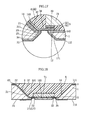
- FIGS. 1 to 3 show an electronic device based on a first embodiment of the present invention.
- An electronic device A 1 of the present embodiment includes a substrate 1 , an insulating layer 2 , a conducting layer 3 , a back surface side insulating film 41 , back surface electrode pads 51 , a sealing resin portion 6 , a main electronic element 71 , and multiple auxiliary electronic elements 8 .
- FIG. 1 is a cross-section taken in the thickness direction of the electronic device A 1 .
- FIG. 2 is an enlarged cross-sectional view showing a relevant portion of the electronic device A 1 .
- FIG. 3 is a plan view showing relevant portions with the sealing resin portion 6 omitted.
- the substrate 1 is formed of a single-crystal semiconductor material.
- the substrate 1 is formed of single-crystal Si in the present embodiment.
- the material of the substrate 1 is not limited to being Si, and may be SiC, for example.
- the thickness of the substrate 1 is 200 to 550 ⁇ m, for example.
- the main electronic element 71 and the auxiliary electronic elements 8 are arranged on the substrate 1 .
- the substrate 1 has a main surface 111 and a back surface 112 .
- the main surface 111 faces one side in the thickness direction.
- the main surface 111 is flat.
- the main surface 111 is orthogonal to the thickness direction.
- the main surface 111 is a (100) surface or a (110) surface. In the present embodiment, the main surface 111 is a (100) surface.
- the back surface 112 faces the other side in the thickness direction. That is, the back surface 112 and the main surface 111 face mutually opposite sides.
- the back surface 112 is flat.
- the back surface 112 is orthogonal to the thickness direction.
- An element arrangement recessed portion 14 and two through-holes 17 are formed in the substrate 1 .
- the element arrangement recessed portion 14 is recessed from the main surface 111 .
- the main electronic element 71 and the multiple auxiliary electronic elements 8 are arranged in the element arrangement recessed portion 14 .
- the depth of the element arrangement recessed portion 14 (distance between the main surface 111 and a later-described element arrangement recessed portion bottom surface 142 in the thickness direction) is 100 to 300 ⁇ m, for example.
- the element arrangement recessed portion 14 is rectangular in a view in the thickness direction.
- the shape of the element arrangement recessed portion 14 depends on the fact that a (100) surface is used as the main surface 111 .
- the element arrangement recessed portion 14 has element arrangement recessed portion side surfaces 141 and an element arrangement recessed portion bottom surface 142 .
- the element arrangement recessed portion bottom surface 142 faces the same side as the main surface 111 in the thickness direction of the substrate 1 .
- the element arrangement recessed portion bottom surface 142 is rectangular in a view in the thickness direction.
- the main electronic element 71 is arranged on the element arrangement recessed portion bottom surface 142 .
- the element arrangement recessed portion bottom surface 142 is a surface that is orthogonal to the thickness direction.
- the element arrangement recessed portion side surfaces 141 rise from the element arrangement recessed portion bottom surface 142 .
- the element arrangement recessed portion side surfaces 141 are connected to the element arrangement recessed portion bottom surface 142 and the main surface 111 .
- the element arrangement recessed portion side surfaces 141 are inclined with respect to the thickness direction.
- the angle of the element arrangement recessed portion side surfaces 141 with respect to a plane orthogonal to the thickness direction is 55 degrees. This is due to the fact that a (100) surface is used as the main surface 111 .
- the element arrangement recessed portion side surfaces 141 are four flat surfaces.
- the through-holes 17 each penetrate a portion of the substrate 1 from the element arrangement recessed portion bottom surface 142 to the back surface 112 .
- the depth of the through-holes 17 is 10 to 50 ⁇ m, for example.
- the dimension of the largest opening of the through-holes 17 in a view in the thickness direction of the substrate 1 is 10 to 50 ⁇ m, for example.
- the ratio of the depth of the through-holes 17 to the dimension of the largest opening of the through-holes 17 in a view in the thickness direction of the substrate 1 is 0.2 to 5.
- the through-holes 17 are rectangular in a view in the thickness direction.
- the cross-sectional dimensions of the through-holes 17 increase toward the back surface 112 starting from the main surface 111 in the thickness direction.
- the through-holes 17 each have through-hole inner surfaces 171 .
- the through-hole inner surfaces 171 are inclined with respect to the thickness direction of the substrate 1 .
- the through-hole inner surfaces 171 are four flat surfaces.
- the through-hole inner surfaces 171 are connected to the element arrangement recessed portion bottom surface 142 and the back surface 112 .
- the angle of the through-hole inner surfaces 171 with respect to a plane orthogonal to the thickness direction is 55 degrees. This is due to the fact that a (100) surface is used as the main surface 111 .
- the insulating layer 2 is interposed between the conducting layer 3 and the substrate 1 .
- the thickness of the insulating layer 2 is about 0.1 to 1.0 ⁇ m, for example.
- the insulating layer 2 is formed of SiO 2 or SiN, for example.
- the insulating layer 2 has a recessed portion inner surface insulating portion 21 , through-hole inner surface insulating portions 22 , auxiliary through-hole inner surface insulating portions 23 , and a back surface side insulating portion 24 .
- the recessed portion inner surface insulating portion 21 is formed in the element arrangement recessed portion 14 of the substrate 1 .
- the recessed portion inner surface insulating portion 21 is formed on all of the element arrangement recessed portion side surfaces 141 and the element arrangement recessed portion bottom surface 142 .
- the recessed portion inner surface insulating portion 21 is formed through thermal oxidation, for example.
- the recessed portion inner surface insulating portion 21 is formed of SiO 2 , for example.
- Auxiliary through-holes 211 are formed in the recessed portion inner surface insulating portion 21 .
- the auxiliary through-holes 211 penetrate the recessed portion inner surface insulating portion 21 in the thickness direction. Also, the auxiliary through-holes 211 are located in the through-holes 17 in a view in the thickness direction.
- the cross-sectional shape of the auxiliary through-holes 211 is constant in the thickness direction.
- the through-hole inner surface insulating portions 22 are formed on the through-hole inner surfaces 171 of the through-holes 17 .
- the through-hole inner surface insulating portions 22 are formed through CVD (Chemical Vapor Deposition), for example.
- the through-hole inner surface insulating portions 22 are formed of SiO 2 or SiN, for example.
- the auxiliary through-hole inner surface insulating portions 23 are formed on the inner surfaces of the auxiliary through-holes 211 of the recessed portion inner surface insulating portions 21 .
- the auxiliary through-hole inner surface insulating portions 23 are formed through CVD (Chemical Vapor Deposition), for example.
- the auxiliary through-hole inner surface insulating portions 23 are formed of SiO 2 or SiN, for example.
- At least a portion of the back surface side insulating portion 24 is formed on the back surface 112 of the substrate 1 .
- the back surface side insulating portion 24 is formed through thermal oxidation.
- the back surface side insulating portion 24 is formed of SiO 2 , for example.
- the conducting layer 3 is electrically connected to the main electronic element 71 and the auxiliary electronic elements 8 .
- the conducting layer 3 is for constituting a current path for performing input to and output from the main electronic element 71 and the auxiliary electronic elements 8 .
- the conducting layer 3 is formed on the element arrangement recessed portion side surfaces 141 , the element arrangement recessed portion bottom surface 142 , the through-hole inner surfaces 171 , and the back surface 112 . More specifically, the conducting layer 3 is formed so as to span from the element arrangement recessed portion 14 to the back surface 112 via the through-hole inner surfaces 171 .
- the conducting layer 3 includes a seed layer 31 and a plating layer 32 .
- the seed layer 31 is a so-called base layer for forming the desired plating layer 32 .
- the seed layer 31 is interposed between the substrate 1 and the plating layer 32 .
- the seed layer 31 is formed of Cu, for example.
- the seed layer 31 is formed through sputtering, for example.
- the thickness of the seed layer 31 is 1 ⁇ m or less, for example.
- the plating layer 32 is formed through electrolytic plating using the seed layer 31 .
- the plating layer 32 is formed of Cu or a layer in which Ti, Ni, Cu, and the like are stacked, for example.
- the thickness of the plating layer 32 is about 3 to 10 ⁇ m, for example.
- the thickness of the plating layer 32 is thicker than the thickness of the seed layer 31 .
- the conducting layer 3 includes element arrangement recessed portion pads 33 , through-hole inner surface conducting portions 35 , auxiliary through-hole blocking portions 36 , and a connection path 37 .
- the element arrangement recessed portion pads 33 are formed in the element arrangement recessed portion 14 , and in particular, are formed on the element arrangement recessed portion bottom surface 142 .
- the element arrangement recessed portion pads 33 formed on the element arrangement recessed portion bottom surface 142 are used for mounting the main electronic element 71 on the element arrangement recessed portion bottom surface 142 .
- the through-hole inner surface conducting portions 35 include portions formed on the through-hole inner surfaces 171 of the through-holes 17 .
- the through-hole inner surface conducting portions 35 include, in the through-hole inner surfaces 171 of the through-holes 17 , portions stacked on the through-hole inner surface insulating portions 22 of the insulating layer 2 , and portions formed on the auxiliary through-hole inner surface insulating portions 23 .
- the through-hole inner surface conducting portions 35 include portions that are arranged so as to form the bottom surfaces of the through-holes 17 and are at a right angle to the thickness direction.
- the auxiliary through-hole blocking portions 36 block the through-holes 17 from the main surface 111 side and form the same layer as the element arrangement recessed portion pads 33 formed on the element arrangement recessed portion bottom surface 142 .
- the auxiliary through-hole blocking portions 36 and the through-hole inner surface conducting portions 35 are in contact with each other.
- connection path 37 forms a path through which the main electronic element 71 and the multiple auxiliary electronic elements 8 mainly are electrically connected.
- the connection path 37 is formed on the element arrangement recessed portion side surface 141 , the element arrangement recessed portion bottom surface 142 , and the main surface 111 .
- a portion of the connection path 37 that is formed on the element arrangement recessed portion side surface 141 is connected in series to the multiple auxiliary electronic elements 8 .
- a portion of the connection path 37 that is formed on the main surface 111 can connect the multiple auxiliary electronic elements 8 in series to each other. Also, if part of the connection path 37 is removed with a later-described method, the connection state of the multiple auxiliary electronic elements 8 is changed.
- the back surface side insulating film 41 is formed on the back surface 112 .
- the back surface side insulating film 41 has portions formed in the through-holes 17 .
- the conducting layer 3 is interposed between the back surface side insulating film 41 and the substrate 1 .
- the back surface side insulating film 41 is formed of SiN, for example.
- the back surface side insulating film 41 is formed through CVD, for example.
- the back surface electrode pads 51 are formed on the back surface 112 .
- the back surface electrode pads 51 are in contact with the conducting layer 3 and are electrically connected to the main electronic element 71 and the auxiliary electronic elements 8 .
- the back surface electrode pads 51 each have a structure in which a Ni layer, a Pd layer, and a Au layer, in order of closeness to the substrate 1 , for example, are stacked. In the present embodiment, the back surface electrode pads 51 are rectangular.
- the sealing resin portion 6 fills the element arrangement recessed portion 14 and covers the main electronic element 71 and the multiple auxiliary electronic elements 8 .
- Examples of the material of the sealing resin portion 6 include epoxy resin, phenol resin, polyimide resin, polybenzoxazole (PBO) resin, and silicone resin.
- the sealing resin portion 6 may be either translucent resin or non-translucent resin, but in the present embodiment, non-translucent resin is preferable.
- a through-hole 63 is formed in the sealing resin portion 6 . The through-hole 63 overlaps with the main surface 111 in a view in the thickness direction and causes part of the portion of the connection path 37 formed on the main surface 111 to be exposed from the sealing resin portion 6 .
- the main electronic element 71 is mounted on the element arrangement recessed portion bottom surface 142 .
- the main electronic element 71 include integrated circuit elements, or more specifically, so-called ASIC (Application Specific Integrated Circuit) elements.
- ASIC Application Specific Integrated Circuit
- other examples of the main electronic element 71 include passive elements such as inductors and capacitors.
- the multiple auxiliary electronic elements 8 are formed on the element arrangement recessed portion side surface 141 .
- the auxiliary electronic elements 8 being formed on the element arrangement recessed portion side surface 141 indicates a mode that is different from a mode in which certain electronic elements are mounted on the element arrangement recessed portion side surface 141 with a bonding method such as solder, for example. That is to say, it indicates a mode in which the main elements constituting the auxiliary electronic-elements 8 are stacked directly or indirectly on the element arrangement recessed portion side surface 141 , a mode in which the main elements constituting the auxiliary electronic elements 8 are included due to part of the element arrangement recessed portion side surface 141 being modified, or the like.
- the multiple auxiliary electronic elements 8 are resistors.
- the auxiliary electronic elements 8 each have a resistive layer 81 .
- the resistive layer 81 is formed on the recessed portion inner surface insulating portion 21 covering the element arrangement recessed portion side surface 141 .
- the resistive layer 81 is formed of a material by which a required resistance can be realized in the resistor, examples of which include silicon-chromium alloy, nickel-chromium alloy, and the like.
- the thickness of the resistive layer 81 is about 5 to 50 nm, for example.
- both end portions of the resistive layer 81 are covered by the connection path 37 . Accordingly, the resistive layer 81 is electrically connected to the connection path 37 .
- the multiple auxiliary electronic elements 8 are formed on the element arrangement recessed portion side surface 141 .
- four auxiliary electronic elements 8 are arranged.
- the two auxiliary electronic elements 8 located at the upper and lower ends in the drawing are incorporated in the current path, and the two auxiliary electronic elements 8 located in the middle are not incorporated in the current path due to the fact that the connection path 37 constitutes a bypass path on the main surface 111 .
- the central portion of the portion of the connection path 37 located on the main surface 111 is removed with a method such as a laser, using the above-described through-hole 63 in the sealing resin portion 6 .
- the four auxiliary electronic elements 8 are directly connected via the remaining connection path 37 .
- the through-hole 63 may be filled with resin or the like.
- the substrate 1 is prepared as shown in FIG. 4 .
- the substrate 1 is formed of a single-crystal semiconductor material, and in the present embodiment, it is formed of single-crystal Si.
- the thickness of the substrate 1 is 200 to 550 ⁇ m, for example.
- the substrate 1 is of a size such that it is possible to obtain multiple substrates 1 for the above-described electronic device A 1 . That is to say, the following manufacturing steps are based on a method for manufacturing multiple electronic devices A 1 at once. It is possible to use a method for manufacturing one electronic device A 1 , but considering industrial efficiency, it is practical to use a method for manufacturing multiple electronic devices A 1 at once. Strictly speaking, the substrate 1 shown in FIG. 4 is different from the substrate 1 in the electronic device A 1 , but in order to facilitate understanding, all substrates are indicated as “substrate 1 ”.
- the substrate 1 has the main surface 111 and the back surface 112 , which face mutually opposite sides.
- a surface whose crystal orientation is (100), that is, a (100) surface is used as the main surface 111 .
- a mask layer formed of SiO 2 is formed through, for example, oxidation of the main surface 111 .
- the thickness of the mask layer is around 0.7 to 1.0 ⁇ m, for example.
- etching is performed on the mask layer. Accordingly, a rectangular opening, for example, is formed in the mask layer.
- the shape and size of the opening is set according to the shape and size of the element arrangement recessed portion 14 that is to ultimately be obtained.
- KOH is an example of an alkali etching solution by which favorable anisotropic etching can be realized for single-crystal Si. Accordingly, a recessed portion is formed in the substrate 1 .
- the recessed portion has a bottom surface and side surfaces. The bottom surface is at a right angle to the thickness direction. The angle that the side surfaces form with respect to a plane that is orthogonal to the thickness direction is about 55°.
- the element arrangement recessed portion 14 shown in FIG. 5 is formed.
- the element arrangement recessed portion 14 has the element arrangement recessed portion side surfaces 141 and the element arrangement recessed portion bottom surface 142 , and is recessed from the main surface 111 .
- the element arrangement recessed portion 14 is rectangular in a view in the thickness direction.
- the insulating layer 2 is formed on the main surface 111 , the element arrangement recessed portion side surfaces 141 and the element arrangement recessed portion bottom surface 142 through thermal oxidation.
- the portion of the insulating layer 2 that covers the element arrangement recessed portion side surfaces 141 and the element arrangement recessed portion bottom surface 142 is to be the above-described recessed portion inner surface insulating portion 21 .
- the resistive layers 81 are formed as shown in FIG. 8 .
- a thin film of silicon-chromium alloy, nickel-chromium alloy, or the like is formed on the entire surface of the insulating layer 2 with a thin film forming method such as sputtering, for example.
- the four resistive layers 81 are formed on the portion of the recessed portion inner surface insulating portion 21 that covers the element arrangement recessed portion side surface 141 .
- the seed layer 31 and the plating layer 32 are formed.
- the seed layer 31 is formed by performing sputtering using Cu, for example, and then carrying out patterning.
- the plating layer 32 is formed through electrolytic plating using the seed layer 31 , for example.
- the plating layer 32 which is formed of Cu or a layer in which Ti, Ni, Cu, and the like are stacked, for example, is obtained.
- the seed layer 31 and the plating layer 32 form the conducting layer 3 by being stacked.
- the conducting layer 3 has a shape in which the element arrangement recessed portion pads 33 and the connection path 37 are included, for example. Also, as shown in FIG.
- connection path 37 has a shape that covers both end portions of the resistive layers 81 . Accordingly, the multiple auxiliary electronic elements 8 are formed. Note that in the etching carried out in the formation of the seed layer 31 and the plating layer 32 , it is desirable that only the material of the seed layer 31 and the plating layer 32 is selectively dissolved and the resistive layer 81 is selectively allowed to remain.
- the main electronic element 71 is arranged in the element arrangement recessed portion 14 as shown in FIG. 11 . More specifically, the main electronic element 71 is mounted on the element arrangement recessed portion bottom surface 142 . Solder balls, for example, are formed on the main electronic element 71 . The solder balls are coated with flax. The main electronic element 71 is mounted using the adhesiveness of the flax. Also, the arrangement of the main electronic element 71 is completed by melting the solder balls with a reflow oven and then allowing them to solidify. Instead of the method of forming solder balls, it is possible to use a method of coating the element arrangement recessed portion pads 33 of the conducting layer 3 with a solder paste.
- the sealing resin portion 6 is formed as shown in FIG. 12 .
- the sealing resin portion 6 is formed, for example, by filling a space surrounded by the element arrangement recessed portion bottom surface 142 and the element arrangement recessed portion side surfaces 141 with a resin material that has excellent permeability and is cured through light exposure, such that the main electronic element 71 is covered, and curing the resin material.
- the sealing resin portion 6 is formed so as to cover the main surface 111 .
- the through-hole 63 is formed by removing a portion of the sealing resin portion 6 .
- the through-holes 17 are formed as shown in FIG. 13 .
- a mask layer formed of SiO 2 is formed through thermal oxidation of the back surface 112 , for example.
- openings are provided in the mask layer at positions corresponding to the through-holes 17 .
- anisotropic etching using KOH, for example, is performed. Accordingly, the through-holes 17 having the through-hole inner surfaces 171 , which are inclined with respect to the thickness direction, are obtained.
- the auxiliary through-holes 211 are formed as shown in FIG. 14 . Specifically, dry etching, for example, is carried out on the portions of the recessed portion inner surface insulating portion 21 of the insulating layer 2 that are exposed from the main electronic element 71 on the back surface 112 side. Accordingly, the auxiliary through-holes 211 with cross-sectional shapes that are constant in the thickness direction are formed at those portions of the recessed portion inner surface insulating portion 21 .
- the through-hole inner surface insulating portions 22 , the auxiliary through-hole inner surface insulating portions 23 , and the back surface side insulating portion 24 are formed as shown in FIGS. 15 and 16 .
- These elements are formed by performing CVD using an insulating material such as SiO 2 or SiN, for example, and then carrying out patterning.
- the seed layer 31 is formed at suitable locations on the through-hole inner surface insulating portions 22 , the auxiliary through-hole inner surface insulating portions 23 , and the back surface side insulating portion 24 of the insulating layer 2 .
- the seed layer 31 is formed by performing sputtering using Cu and then carrying out patterning, for example.
- the plating layer 32 is formed at suitable locations on the through-hole inner surface insulating portions 22 , the auxiliary through-hole inner surface insulating portions 23 , and the back surface side insulating portion 24 of the insulating layer 2 .
- the plating layer 32 is formed through electrolytic plating using the seed layer 31 , for example.
- the plating layer 32 which is formed of Cu or a layer in which Ti, Ni, Cu, and the like are stacked, for example, is obtained.
- the through-hole inner surface conducting portions 35 of the conducting layer 3 are formed.
- the back surface side insulating film 41 is formed as shown in FIG. 19 .
- the back surface side insulating film 41 is formed by performing CVD using SiN, for example, and then carrying out patterning. Thereafter, the back surface electrode pads 51 are formed.
- the back surface electrode pads 51 are formed through non-electrolytic plating with a metal such as Ni, Pd, or Au, for example.
- the substrate 1 is cut with a dicer, for example, whereby the electronic device A 1 shown in FIGS. 1 and 2 is obtained.
- the auxiliary electronic elements 8 are formed on the element arrangement recessed portion side surface 141 .
- the main elements of the auxiliary electronic elements 8 are formed directly or indirectly on the element arrangement recessed portion side surface 141 .
- the arrangement accuracy of the auxiliary electronic elements 8 can be significantly increased, which contributes to a smaller size and high-density arrangement of the auxiliary electronic elements 8 . Accordingly, it is possible to achieve a smaller size of the electronic device A 1 .
- the resistive layer 81 By forming the resistive layer 81 on the recessed portion inner surface insulating portion 21 on which a relatively smooth surface can be formed, it is possible to form a resistive layer 81 that is finer and thinner. This makes it suitable for setting the resistance of the auxiliary electronic elements 8 serving as resistors to a desired value.
- the through-holes 17 that penetrate from the element arrangement recessed portion 14 to the back surface 112 are formed in the substrate 1 .
- the conducting layer 3 is formed so as to extend from the element arrangement recessed portion 14 to the back surface 112 via the through-hole inner surfaces 171 . According to this configuration, a current path from the element arrangement recessed portion side to the back surface 112 side can be formed. According to this, a configuration is realized in which an electrical connection path that is needed for causing the main electronic element 71 to operate overlaps with the main electronic element 71 in a view in the thickness direction, for example. Accordingly, this is suitable for achieving a smaller size of the electronic device A 1 in a view in the thickness direction.
- the element arrangement recessed portion side surfaces 141 are inclined with respect to the thickness direction Z. According to this configuration, the element arrangement recessed portion side surfaces 141 can be formed so as to be relatively flat. For this reason, the advantage that the seed layer 31 (i.e., the conducting layer 3 ) is easier to form can be obtained.
- the through-hole inner surfaces 171 are inclined with respect to a thickness direction Z. According to this configuration, the through-hole inner surfaces 171 can be formed so as to be relatively flat. For this reason, the advantage that the seed layer 31 (i.e., the conducting layer 3 ) is easier to form can be obtained.
- the auxiliary through-hole blocking portions 36 and the through-hole inner surface conducting portions 35 are in contact at the boundary portions between the element arrangement recessed portion 14 (element arrangement recessed portion bottom surface 142 ) and the through-holes 17 .
- This contact is achieved in a surface area corresponding to the surface area of the bottom portions of the through-holes 17 . Accordingly, it is possible to more reliably electrically connect the auxiliary through-hole blocking portions 36 and the through-hole inner surface conducting portions 35 , or in other words, the portions of the conducting layer 3 that are formed on the back surface 112 side and the portions of the conducting layer 3 that are formed on the element arrangement recessed portion 14 side.
- FIGS. 20 to 22 show other embodiments of the present invention. Note that in these drawings, elements that are the same as or similar to those in the above-described embodiment are denoted by the same reference numerals as in the above-described embodiment.
- FIG. 20 shows an electronic device based on a second embodiment of the present invention.
- An electronic device A 2 of the present embodiment differs from that of the above-described embodiment mainly in the configuration of the auxiliary electronic elements 8 .
- the recessed portion inner surface insulating portion 21 of the insulating layer 2 is formed of a first insulating layer 212 and a second insulating layer 213 .
- This kind of configuration may be used in the entirety of the insulating layer 2 , or in the entirety of the recessed portion inner surface insulating portion 21 , or it may be applied to only the site shown in FIG. 19 .
- the first insulating layer 212 and the second insulating layer 213 are formed of the same material as the above-described recessed portion inner surface insulating portion 21 .
- the resistive layer 81 is formed on the first insulating layer 212 .
- the second insulating layer 213 covers most of the resistive layer 81 .
- Multiple through-holes 213 a are formed in the second insulating layer 213 .
- the through-holes 213 a penetrate the second insulating layer 213 .
- the through-holes 213 a cause the portions near both ends of the resistive layer 81 to be exposed from the second insulating layer 213 .
- connection path 37 is formed on the second insulating layer 213 .
- the connection path 37 fills the through-holes 213 a of the second insulating layer 213 and is electrically connected to the resistive layer 81 through the through-holes 213 a.
- the resistive layer 81 is formed on the first insulating layer 212 , whereafter the second insulating layer 213 is formed. Thereafter, a metal layer for forming the connection path 37 is formed by means of plating and is subjected to etching, and the like. In the etching, the resistive layer 81 is covered by the second insulating layer 213 , and thus is not exposed to the etching liquid. Accordingly, the etching for forming the connection path 37 is advantageous in that it is not limited to being such that only the material of the connection path 37 is selectively dissolved and the resistive layer 81 is selectively allowed to remain.
- FIG. 21 shows an electronic device based on a third embodiment of the present invention.
- An electronic device A 3 of the present embodiment differs from that of the above-described embodiments mainly in the configuration of the auxiliary electronic elements 8 .
- the resistive layer 81 is formed by modifying a portion of the element arrangement recessed portion side surface 141 . More specifically, a dopant, which is an added impurity element, is implanted into the region of the element arrangement recessed portion side surface 141 in which the resistive layer 81 is to be formed. A dopant is used which modifies Si or the like, which is the material of the substrate 1 , into a conductor having a desired resistance. Also, in order to electrically disconnect the main body of the substrate 1 and the resistive layer 81 , doping for forming an electrical disconnection region, such as an insulating region or a pn junction region, may be performed in addition to doping for forming the resistive layer 81 .
- an electrical disconnection region such as an insulating region or a pn junction region
- the resistive layer 81 is provided integrally in the element arrangement recessed portion side surface 141 and is covered by the recessed portion inner surface insulating portion 21 .
- Through-holes 21 a that cause suitable locations on the resistive layer 81 to be exposed from the recessed portion inner surface insulating portion 21 are formed on the recessed portion inner surface insulating portion 21 .
- the connection path 37 is electrically connected to the resistive layer 81 through the through-holes 21 a.
- FIG. 22 shows an electronic device based on a fourth embodiment of the present invention.
- An electronic device A 4 of the present embodiment differs from the above-described embodiments mainly in the configuration of the auxiliary electronic elements 8 .
- the auxiliary electronic elements 8 are each configured as a capacitor.
- Each auxiliary electronic element 8 has a first electrode layer 82 , a second electrode layer 83 , and a dielectric layer 84 .
- the recessed portion inner surface insulating portion 21 is configured to include the first insulating layer 212 , the second insulating layer 213 , and a third insulating layer 214 .
- the first insulating layer 212 is a layer formed on the element arrangement recessed portion side surface 141 .
- the first electrode layer 82 is formed on the first insulating layer 212 and forms one of the electrodes of the auxiliary electronic element 8 serving as a capacitor.
- the first electrode layer 82 is of a size at which it is possible to achieve a desired capacitance, and is rectangular, for example.
- the first electrode layer 82 is formed of a conductor such as Cu.
- the dielectric layer 84 is interposed between the first electrode layer 82 and the second electrode layer 83 , and thereby functions as a dielectric portion of the auxiliary electronic element 8 serving as a capacitor.
- the dielectric layer 84 is constituted by a portion of the second insulating layer 213 .
- a through-hole 213 a that causes a portion of the first electrode layer 82 to be exposed from the second insulating layer 213 is formed in the second insulating layer 213 .
- the second insulating layer 213 constituting the dielectric layer 84 is preferably formed of a ferroelectric material.
- the second electrode layer 83 is formed on the second insulating layer 213 and forms the other of the electrodes of the auxiliary electronic element 8 serving as a capacitor.
- the second electrode layer 83 is of a size at which it is possible to achieve a desired capacitance, and is rectangular, for example.
- the second electrode layer 83 is formed of a conductor such as Cu.
- the third insulating layer 214 covers the second electrode layer 83 . However, in the present embodiment, the third insulating layer 214 does not cover the through-hole 213 a of the second insulating layer 213 .
- a through-hole 214 a is formed in the third insulating layer 214 . The through-hole 214 a causes a portion of the dielectric layer 84 to be exposed from the third insulating layer 214 .
- connection path 37 is electrically connected to the first electrode layer 82 through the through-hole 213 a . Also, another portion of the connection path 37 is electrically connected to the second electrode layer 83 through the through-hole 214 a.
- the specific configuration in which the auxiliary electronic elements 8 are included as capacitors is not limited to the configuration of the electronic device A 4 .
- the first electrode layer 82 may be formed by modifying a portion of the element arrangement recessed portion side surface 141 as was described in the case of the electronic device A 3 .
- auxiliary electronic elements 8 it is possible to achieve a smaller size of the electronic device A 4 .
- auxiliary electronic elements 8 there is no limitation on the function of the auxiliary electronic elements 8 , and they may function as various kinds of electronic elements, such as resistors, capacitors, and the like.
- the auxiliary electronic elements 8 function as inductors, for example, by using a method similar to those of the electronic devices A 1 to A 4 .
- multiple auxiliary electronic elements that perform mutually different functions may be provided in one electronic device according to the present invention.
- the electronic device according to the present invention is not limited to the above-described embodiments.
- the specific configuration of the units of the electronic device according to the present invention can be designed and modified in various ways.
Landscapes
- Engineering & Computer Science (AREA)
- Microelectronics & Electronic Packaging (AREA)
- Physics & Mathematics (AREA)
- Condensed Matter Physics & Semiconductors (AREA)
- General Physics & Mathematics (AREA)
- Computer Hardware Design (AREA)
- Power Engineering (AREA)
- Internal Circuitry In Semiconductor Integrated Circuit Devices (AREA)
- Ceramic Engineering (AREA)
- Manufacturing & Machinery (AREA)
- Geometry (AREA)
Abstract
Description
Claims (25)
Applications Claiming Priority (2)
| Application Number | Priority Date | Filing Date | Title |
|---|---|---|---|
| JP2014264393A JP2016127048A (en) | 2014-12-26 | 2014-12-26 | Electronic equipment |
| JP2014-264393 | 2014-12-26 |
Publications (2)
| Publication Number | Publication Date |
|---|---|
| US20160190051A1 US20160190051A1 (en) | 2016-06-30 |
| US9698092B2 true US9698092B2 (en) | 2017-07-04 |
Family
ID=56165080
Family Applications (1)
| Application Number | Title | Priority Date | Filing Date |
|---|---|---|---|
| US14/757,968 Expired - Fee Related US9698092B2 (en) | 2014-12-26 | 2015-12-24 | Electronic device |
Country Status (2)
| Country | Link |
|---|---|
| US (1) | US9698092B2 (en) |
| JP (1) | JP2016127048A (en) |
Citations (2)
| Publication number | Priority date | Publication date | Assignee | Title |
|---|---|---|---|---|
| US6091027A (en) * | 1996-12-19 | 2000-07-18 | Telefonaktiebolaget Lm Ericsson | Via structure |
| JP2012099673A (en) | 2010-11-02 | 2012-05-24 | Ricoh Co Ltd | Semiconductor package and electronic-component mounted body |
-
2014
- 2014-12-26 JP JP2014264393A patent/JP2016127048A/en active Pending
-
2015
- 2015-12-24 US US14/757,968 patent/US9698092B2/en not_active Expired - Fee Related
Patent Citations (3)
| Publication number | Priority date | Publication date | Assignee | Title |
|---|---|---|---|---|
| US6091027A (en) * | 1996-12-19 | 2000-07-18 | Telefonaktiebolaget Lm Ericsson | Via structure |
| JP2012099673A (en) | 2010-11-02 | 2012-05-24 | Ricoh Co Ltd | Semiconductor package and electronic-component mounted body |
| US8415811B2 (en) | 2010-11-02 | 2013-04-09 | Ricoh Company, Ltd. | Semiconductor package and electronic component package |
Also Published As
| Publication number | Publication date |
|---|---|
| US20160190051A1 (en) | 2016-06-30 |
| JP2016127048A (en) | 2016-07-11 |
Similar Documents
| Publication | Publication Date | Title |
|---|---|---|
| JP4674606B2 (en) | Thin film capacitor | |
| US6744122B1 (en) | Semiconductor device, method of manufacture thereof, circuit board, and electronic device | |
| US9585254B2 (en) | Electronic device | |
| CN105814687B (en) | Semiconductor package and its mounting structure | |
| CN102077341B (en) | Packaged semiconductor product and manufacturing method thereof | |
| CN208061869U (en) | Thin film type LC component and its mounting structure | |
| JPWO2016121491A1 (en) | Electronic circuit module | |
| CN107535080B (en) | Electronic circuit module | |
| CN105280567A (en) | Semiconductor package and manufacturing method therefor | |
| CN100552926C (en) | Semiconductor device, wiring board and method for manufacturing the same | |
| TWI651741B (en) | Semiconductor device with capacitor | |
| CN207425835U (en) | Thin-film device | |
| US9899360B2 (en) | Semiconductor device | |
| US20200126898A1 (en) | Electronic component module | |
| CN109791840B (en) | Electronic component | |
| JP6533066B2 (en) | Electronic device | |
| CN207572353U (en) | thin film device | |
| US9698092B2 (en) | Electronic device | |
| JP4752280B2 (en) | Chip-type electronic component and manufacturing method thereof | |
| CN102190279A (en) | Semiconductor device | |
| JP2017005073A (en) | Manufacturing method of electronic device | |
| JP7099838B2 (en) | Chip parts and manufacturing methods for chip parts | |
| JP2018152437A (en) | Circuit board, electronic device, and circuit board manufacturing method | |
| JP7154818B2 (en) | Semiconductor device and method for manufacturing semiconductor device | |
| JP6730495B2 (en) | Electronic device |
Legal Events
| Date | Code | Title | Description |
|---|---|---|---|
| AS | Assignment |
Owner name: ROHM CO., LTD., JAPAN Free format text: ASSIGNMENT OF ASSIGNORS INTEREST;ASSIGNOR:NISHIMURA, ISAMU;REEL/FRAME:041768/0209 Effective date: 20150924 |
|
| STCF | Information on status: patent grant |
Free format text: PATENTED CASE |
|
| MAFP | Maintenance fee payment |
Free format text: PAYMENT OF MAINTENANCE FEE, 4TH YEAR, LARGE ENTITY (ORIGINAL EVENT CODE: M1551); ENTITY STATUS OF PATENT OWNER: LARGE ENTITY Year of fee payment: 4 |
|
| FEPP | Fee payment procedure |
Free format text: MAINTENANCE FEE REMINDER MAILED (ORIGINAL EVENT CODE: REM.); ENTITY STATUS OF PATENT OWNER: LARGE ENTITY |
|
| LAPS | Lapse for failure to pay maintenance fees |
Free format text: PATENT EXPIRED FOR FAILURE TO PAY MAINTENANCE FEES (ORIGINAL EVENT CODE: EXP.); ENTITY STATUS OF PATENT OWNER: LARGE ENTITY |
|
| STCH | Information on status: patent discontinuation |
Free format text: PATENT EXPIRED DUE TO NONPAYMENT OF MAINTENANCE FEES UNDER 37 CFR 1.362 |
|
| FP | Lapsed due to failure to pay maintenance fee |
Effective date: 20250704 |