US9688914B2 - Liquid crystal material and liquid crystal display device including the same - Google Patents

Liquid crystal material and liquid crystal display device including the same Download PDF

Info

Publication number
US9688914B2
US9688914B2 US14/292,514 US201414292514A US9688914B2 US 9688914 B2 US9688914 B2 US 9688914B2 US 201414292514 A US201414292514 A US 201414292514A US 9688914 B2 US9688914 B2 US 9688914B2
Authority
US
United States
Prior art keywords
liquid crystal
phenol
based antioxidant
lcd device
light stabilizer
Prior art date
Legal status (The legal status is an assumption and is not a legal conclusion. Google has not performed a legal analysis and makes no representation as to the accuracy of the status listed.)
Expired - Fee Related, expires
Application number
US14/292,514
Other versions
US20150002797A1 (en
Inventor
Seung-Kwang ROH
Woo-young Choi
Current Assignee (The listed assignees may be inaccurate. Google has not performed a legal analysis and makes no representation or warranty as to the accuracy of the list.)
LG Display Co Ltd
Original Assignee
LG Display Co Ltd
Priority date (The priority date is an assumption and is not a legal conclusion. Google has not performed a legal analysis and makes no representation as to the accuracy of the date listed.)
Filing date
Publication date
Application filed by LG Display Co Ltd filed Critical LG Display Co Ltd
Assigned to LG DISPLAY CO., LTD. reassignment LG DISPLAY CO., LTD. ASSIGNMENT OF ASSIGNORS INTEREST (SEE DOCUMENT FOR DETAILS). Assignors: CHOI, WOO-YOUNG, ROH, SEUNG-KWANG
Publication of US20150002797A1 publication Critical patent/US20150002797A1/en
Application granted granted Critical
Publication of US9688914B2 publication Critical patent/US9688914B2/en
Expired - Fee Related legal-status Critical Current
Adjusted expiration legal-status Critical

Links

Images

Classifications

    • GPHYSICS
    • G02OPTICS
    • G02FOPTICAL DEVICES OR ARRANGEMENTS FOR THE CONTROL OF LIGHT BY MODIFICATION OF THE OPTICAL PROPERTIES OF THE MEDIA OF THE ELEMENTS INVOLVED THEREIN; NON-LINEAR OPTICS; FREQUENCY-CHANGING OF LIGHT; OPTICAL LOGIC ELEMENTS; OPTICAL ANALOGUE/DIGITAL CONVERTERS
    • G02F1/00Devices or arrangements for the control of the intensity, colour, phase, polarisation or direction of light arriving from an independent light source, e.g. switching, gating or modulating; Non-linear optics
    • G02F1/01Devices or arrangements for the control of the intensity, colour, phase, polarisation or direction of light arriving from an independent light source, e.g. switching, gating or modulating; Non-linear optics for the control of the intensity, phase, polarisation or colour 
    • G02F1/13Devices or arrangements for the control of the intensity, colour, phase, polarisation or direction of light arriving from an independent light source, e.g. switching, gating or modulating; Non-linear optics for the control of the intensity, phase, polarisation or colour  based on liquid crystals, e.g. single liquid crystal display cells
    • CCHEMISTRY; METALLURGY
    • C09DYES; PAINTS; POLISHES; NATURAL RESINS; ADHESIVES; COMPOSITIONS NOT OTHERWISE PROVIDED FOR; APPLICATIONS OF MATERIALS NOT OTHERWISE PROVIDED FOR
    • C09KMATERIALS FOR MISCELLANEOUS APPLICATIONS, NOT PROVIDED FOR ELSEWHERE
    • C09K19/00Liquid crystal materials
    • C09K19/52Liquid crystal materials characterised by components which are not liquid crystals, e.g. additives with special physical aspect: solvents, solid particles
    • C09K19/54Additives having no specific mesophase characterised by their chemical composition
    • CCHEMISTRY; METALLURGY
    • C09DYES; PAINTS; POLISHES; NATURAL RESINS; ADHESIVES; COMPOSITIONS NOT OTHERWISE PROVIDED FOR; APPLICATIONS OF MATERIALS NOT OTHERWISE PROVIDED FOR
    • C09KMATERIALS FOR MISCELLANEOUS APPLICATIONS, NOT PROVIDED FOR ELSEWHERE
    • C09K19/00Liquid crystal materials
    • C09K19/52Liquid crystal materials characterised by components which are not liquid crystals, e.g. additives with special physical aspect: solvents, solid particles

Definitions

  • the present invention relates to a liquid crystal display (LCD) device, and more particularly, to a liquid crystal material having improved reliability and response time and an LCD device including the liquid crystal material.
  • LCD liquid crystal display
  • the LCD device uses optical anisotropy and polarization properties of liquid crystal molecules.
  • the liquid crystal molecules have a definite alignment direction as a result of their thin and long shapes.
  • the alignment direction of the liquid crystal molecules can be controlled by application of an electric field across the liquid crystal molecules. As the intensity or direction of the electric field is changed, the alignment of the liquid crystal molecules also changes. Since incident light is refracted based on the orientation of the liquid crystal molecules due to the optical anisotropy of the liquid crystal molecules, images can be displayed by controlling light transmissivity.
  • the LCD device including a thin film transistor (TFT) as a switching element referred to as an active matrix LCD (AM-LCD) device
  • TFT thin film transistor
  • AM-LCD active matrix LCD
  • the LCD device includes two substrates facing each other and a liquid crystal layer therebetween.
  • the LCD device further includes a pixel electrode and a common electrode for generating an electric field.
  • the liquid crystal layer is driven by the electric field.
  • the LCD device is used for repeatedly displaying similar images in a public place. It may be called to as a public display. Since the public display repeatedly displays similar images in very long times, the reliability of the LCD device is an important fact.
  • the displayed images remain in the screen as an afterimages, and the image quality of the public display is degraded by the afterimages.
  • high reliability is required in the LCD device as the public display.
  • the LCD device for the public display having high reliability has a disadvantage in a response time.
  • the LCD device for the public display having the high response time has a disadvantage in the reliability.
  • the present invention is directed to a liquid crystal material and an LCD device including the same that substantially obviate one or more of the problems due to limitations and disadvantages of the related art.
  • An object of the present invention is to provide a liquid crystal material having advantages in both of the reliability and the response time.
  • Another object of the present invention is to an LCD device including the liquid crystal material.
  • the present invention provides a liquid crystal material including: a liquid crystal molecule including an alkenyl group; a phenol-based antioxidant; and a light stabilizer for recycling the phenol-based antioxidant.
  • the present invention provides a liquid crystal display device including: first and second substrates facing each other; a pixel electrode on the first substrate; a common electrode on one of the first and second substrates; first and second alignment layers respectively over the first and second substrates; and a liquid crystal layer positioned between the first and second alignment layers, the liquid crystal layer including: a liquid crystal molecule including an alkenyl group; a phenol-based antioxidant; and a light stabilizer for recycling the phenol-based antioxidant.
  • FIGS. 1A and 1B are graphs showing a relation between the reliability and the response time in a liquid crystal material according to an embodiment of the present invention.
  • FIG. 2 is a schematic cross-sectional view of an LCD device according to an embodiment of the present invention.
  • FIG. 3 is a view illustrating a reaction mechanism of a phenol-based antioxidant and a radical according to an embodiment of the present invention.
  • FIG. 4 is a view illustrating a recycle mechanism of a phenol-based antioxidant by HALS in a liquid crystal material of the present invention.
  • FIG. 5 is a graph showing an increase of the reliability in an LCD device including a liquid crystal material of the present invention.
  • the liquid crystal material which does not include an alkenyl group, is used.
  • FIG. 1A is a graph showing a relation between the reliability and the alkenyl group content in the liquid crystal material
  • the alkenyl group content in the liquid crystal material is increased, the displaying reliability of the LCD device is decreased. Accordingly, the liquid crystal material without the alkenyl group is used for the LCD device as the public display.
  • FIG. 1B is a graph showing a relation between the response time and the alkenyl group content in the liquid crystal material, as the alkenyl group content in the liquid crystal material is decreased, the response time of the LCD device is decreased.
  • FIG. 2 is a schematic cross-sectional view of an LCD device.
  • the LCD device includes a first substrate 110 , a second substrate 120 facing the first substrate 110 , and a liquid crystal layer 130 between the first and second substrates 110 and 120 .
  • a pixel electrode 170 and a common electrode 172 are formed on the first substrate 110 .
  • An electric field is generated between the pixel and common electrodes 170 and 172 such that the liquid crystal layer 130 is driven.
  • a color filter layer 182 is formed on the second substrate 120 .
  • a plurality of pixel regions are defined in the first substrate 110 , and a thin film transistor (TFT), the pixel electrode 170 and the common electrode 172 are formed in each pixel region.
  • TFT thin film transistor
  • the pixel region is defined by a gate line (not shown) and a data line (not shown) crossing each other.
  • the TFT is connected to the gate and data lines.
  • the TFT includes a gate electrode 142 , a gate insulating layer 144 , a semiconductor layer 150 , a source electrode 162 and a drain electrode 164 .
  • the gate electrode 142 is connected to the gate line, and the gate insulating layer 144 is formed on the gate electrode 142 .
  • the semiconductor layer 150 is formed on the gate insulating layer 144 and overlaps the gate electrode 142 .
  • the semiconductor layer 150 may includes an active layer 152 of an intrinsic amorphous silicon and an ohmic contact layer 154 of an impurity-doped amorphous silicon.
  • the semiconductor layer 150 may include an oxide semiconductor material or poly-crystalline silicon.
  • the source electrode 162 and the drain electrode 164 are formed on the semiconductor layer 150 and are spaced apart from each other.
  • the source electrode 162 is connected to the data line.
  • a passivation layer 166 is formed on the TFT, and a drain contact hole 168 exposing the drain electrode 164 of the TFT is formed through the passivation layer 166 .
  • the pixel electrode 170 and the common electrode 172 are formed on the passivation layer 166 .
  • the pixel electrode 170 and the common electrode 172 are alternately arranged with each other such that a horizontal electric field is generated between the pixel and common electrodes 170 and 172 .
  • the pixel electrode 170 contacts and is electrically connected to the drain electrode 164 of the TFT through the drain contact hole 168 .
  • the pixel and common electrodes have the plate shape, and one of the pixel and common electrodes has an opening. In this instance, the pixel and common electrodes are positioned in different layers such that a fringe field is generated between the pixel and common electrodes.
  • the pixel electrode is formed on the first substrate 110
  • the common electrode is formed on the second substrate 120 . In this instance, a vertical electric field is generated between the pixel and common electrodes.
  • a first alignment layer 174 is formed on the pixel and common electrodes 170 and 172 .
  • the first alignment layer 174 may be formed of polyimide.
  • a black matrix 180 for shielding a non-display area, such as the TFT, the gate line and the data line, and a color filter layer 182 are formed on the second substrate 120 .
  • the black matrix 180 and the color filter layer 182 may be omitted.
  • a second alignment layer 184 is formed on the color filter layer 182 .
  • the second alignment layer 184 may be formed of polyimide.
  • the liquid crystal layer 130 is positioned between the first and second substrates 110 and 120 , and more particularly, between the first and second alignment layers 174 and 184 .
  • the liquid crystal layer 130 includes a liquid crystal molecule 132 , a phenol-based antioxidant 134 and a light stabilizer 136 .
  • An initial arrangement of the liquid crystal molecule 132 is controlled by the first and second alignment layers 174 and 184 , and the liquid crystal molecule 132 includes an alkenyl group for increasing the response time.
  • the alkenyl group is linked to an end of the liquid crystal molecule 132 such that the response time of the liquid crystal layer 130 is improved as shown in FIG. 1B .
  • liquid crystal molecule 132 includes the alkenyl group to increase the response time
  • a by-product is generated by reaction between the alkenyl group in the liquid crystal molecule 132 and a radical or an ion from the first and second alignment layers 174 and 184 such that the reliability of the LCD device is degraded.
  • the LCD device includes a backlight unit as a light source, and the first and second alignment layers 174 and 184 are exposed to a UV from the backlight unit or the outside.
  • the first and second alignment layers 174 and 184 includes a functional group, such as “ROOH”, at their end to control the arrangement of the liquid crystal molecule 132 , and unstable radicals or ions are generated from the functional group of the first and second alignment layers 174 and 184 by the UV.
  • the radicals or ions react with the alkenyl group, which includes the double bond linkage, such that the by-product is generated. The reliability of the LCD device is degraded by the by-product.
  • the liquid crystal layer 130 of the present invention includes a phenol-based antioxidant 134 .
  • the phenol-based antioxidant 134 is represented by following Formula 1.
  • each of R1 and R2 is selected from substituted or non-substituted alkyl group or hydrogen
  • R3 is selected from substituted or non-substituted alkyl group, substituted or non-substituted alkyl-carbonyl group, substituted or non-substituted alkoxy group and hydrogen.
  • liquid crystal layer 130 of the present invention further includes the light stabilizer 136 such that a side reaction generating the by-product is prevented and the phenol-based antioxidant 134 is recycled. As a result, the reliability of the LCD device is further improved.
  • the light stabilizer 136 is represented by following Formula 2. Namely, the light stabilizer 136 is a hindered amine light stabilizer (HALS).
  • HALS hindered amine light stabilizer
  • each of R4 and R5 is selected from hydrogen and substituted or non-substituted alkyl group
  • R6 is selected from hydrogen and substituted or non-substituted alkoxy group.
  • the phenol-based antioxidant 134 and the light stabilizer 136 have excellent solubility with the liquid crystal molecule 132 and excellent transmissivity. As a result, there is no problem in the driving property and the transmissivity of the liquid crystal layer 130 by the phenol-based antioxidant 134 and the light stabilizer 136 .
  • the phenol-based antioxidant 134 reacts with the radicals or ions from the first and second alignment layers 174 and 184 such that the reaction between the radicals or the ions and the alkenyl group in the liquid crystal molecule 132 .
  • the degradation of the reliability of the LCD device by the by-product from the reaction between the radicals or ions and the alkenyl group in the liquid crystal molecule 132 is prevented.
  • FIG. 3 which is a view illustrating a reaction mechanism of a phenol-based antioxidant and a radical
  • the phenol-base antioxidant reacts with the radicals (or ions) such that the radicals becomes stable.
  • the side reaction between the radicals and the alkenyl group in the liquid crystal molecule is prevented.
  • the phenol-based antioxidant is finally changed into a quinone-derivative by the reaction with the radicals.
  • the phenol-base antioxidant does not have a function as the antioxidant. Accordingly, the reliability is increased by the phenol-based antioxidant in an initial driving state.
  • the quinine-derivative serves as impurities in the liquid crystal layer such that the driving property of the liquid crystal layer is degraded.
  • the HALS as the light stabilizer reacts with the radicals (or ions) such the radicals becomes stable.
  • the phenol-based antioxidant is recycled by the HALS.
  • FIG. 4 is a view illustrating a recycle mechanism of a phenol-based antioxidant by HALS in a liquid crystal material of the present invention
  • the phenol-based antioxidant reacts with the radicals to stabilizer the radicals, and the quinine-derivative, as a product of the reaction between the phenol-based antioxidant and the radicals, is recycled by the HALS such that the function of the antioxidant is maintained.
  • the stabilization reaction of the radicals by the phenol-based antioxidant is continuously generated and the degradation of the operation property of the liquid crystal layer by the quinine-derivative is prevented.
  • a voltage holding ratio (VHR, %) according to a time is measured with various cases, i.e., the liquid crystal layer including the liquid crystal molecules having alkenyl group without the phenol-base antioxidant and the HALS (case A), the liquid crystal layer including the liquid crystal molecules having alkenyl group with the phenol-base antioxidant and without the HALS (case B), the liquid crystal layer including the liquid crystal molecules having alkenyl group with HALS and without the phenol-base antioxidant (case C), and the liquid crystal layer including the liquid crystal molecules having alkenyl group with the phenol-base antioxidant and the HALS (case D).
  • the phenol-based antioxidant represented by following Formula 3 is used, and the HALS represent by following Formula 4 is used.
  • the phenol-based antioxidant is added by 1000 weight ppm with respect to the liquid crystal molecule, and the HALS is added by 250 weight ppm with respect to the liquid crystal molecule.
  • FIG. 5 which is a graph showing an increase of the reliability in an LCD device including a liquid crystal material of the present invention
  • the voltage holding ratio in the case B and the case C is higher than the case A. Namely, the reliability of the LCD device is improved by the phenol-based antioxidant and by the HALS.
  • the case D has a similar driving property to the cases A, B and C, while the voltage holding ratio of the case D is rapidly increased after the long-time operation. Namely, as mentioned above, since the phenol-based antioxidant is recycled by the HALS, the reaction between the phenol-based antioxidant and the radicals (or ions) is continuously generated such that the reliability of the LCD device is remarkably increased.

Landscapes

  • Chemical & Material Sciences (AREA)
  • Crystallography & Structural Chemistry (AREA)
  • Engineering & Computer Science (AREA)
  • Materials Engineering (AREA)
  • Organic Chemistry (AREA)
  • Physics & Mathematics (AREA)
  • Nonlinear Science (AREA)
  • General Physics & Mathematics (AREA)
  • Optics & Photonics (AREA)
  • Liquid Crystal (AREA)
  • Liquid Crystal Substances (AREA)
  • Spectroscopy & Molecular Physics (AREA)
  • Mathematical Physics (AREA)

Abstract

Discussed is a liquid crystal material including: a liquid crystal molecule including an alkenyl group; a phenol-based antioxidant; and a light stabilizer for recycling the phenol-based antioxidant.

Description

The present application claims the benefit of Korean Patent Application No. 10-2013-0075528 filed in Republic of Korea on Jun. 28, 2013, which is hereby incorporated by reference for all purposes as if fully set forth herein.
BACKGROUND OF THE INVENTION
Field of the Invention
The present invention relates to a liquid crystal display (LCD) device, and more particularly, to a liquid crystal material having improved reliability and response time and an LCD device including the liquid crystal material.
Discussion of the Related Art
As the society has entered in earnest upon an information age, various display devices, such as an LCD device and an organic light emitting diode (OLED) display device, for displaying images are required.
The LCD device uses optical anisotropy and polarization properties of liquid crystal molecules. The liquid crystal molecules have a definite alignment direction as a result of their thin and long shapes. The alignment direction of the liquid crystal molecules can be controlled by application of an electric field across the liquid crystal molecules. As the intensity or direction of the electric field is changed, the alignment of the liquid crystal molecules also changes. Since incident light is refracted based on the orientation of the liquid crystal molecules due to the optical anisotropy of the liquid crystal molecules, images can be displayed by controlling light transmissivity.
Since the LCD device including a thin film transistor (TFT) as a switching element, referred to as an active matrix LCD (AM-LCD) device, has excellent characteristics of high resolution and displaying moving images, the AM-LCD device has been widely used.
The LCD device includes two substrates facing each other and a liquid crystal layer therebetween. The LCD device further includes a pixel electrode and a common electrode for generating an electric field. The liquid crystal layer is driven by the electric field.
For example, the LCD device is used for repeatedly displaying similar images in a public place. It may be called to as a public display. Since the public display repeatedly displays similar images in very long times, the reliability of the LCD device is an important fact.
Namely, in the public display, the displayed images remain in the screen as an afterimages, and the image quality of the public display is degraded by the afterimages. As a result, high reliability is required in the LCD device as the public display.
However, the LCD device for the public display having high reliability has a disadvantage in a response time. The LCD device for the public display having the high response time has a disadvantage in the reliability.
SUMMARY OF THE INVENTION
Accordingly, the present invention is directed to a liquid crystal material and an LCD device including the same that substantially obviate one or more of the problems due to limitations and disadvantages of the related art.
An object of the present invention is to provide a liquid crystal material having advantages in both of the reliability and the response time.
Another object of the present invention is to an LCD device including the liquid crystal material.
Additional features and advantages of the invention will be set forth in the description which follows, and in part will be apparent from the description, or may be learned by practice of the invention. These and other advantages of the invention will be realized and attained by the structure particularly pointed out in the written description and claims hereof as well as the appended drawings.
To achieve these and other advantages and in accordance with the purpose of the present invention, as embodied and broadly described herein, the present invention provides a liquid crystal material including: a liquid crystal molecule including an alkenyl group; a phenol-based antioxidant; and a light stabilizer for recycling the phenol-based antioxidant.
In another aspect of the present invention, the present invention provides a liquid crystal display device including: first and second substrates facing each other; a pixel electrode on the first substrate; a common electrode on one of the first and second substrates; first and second alignment layers respectively over the first and second substrates; and a liquid crystal layer positioned between the first and second alignment layers, the liquid crystal layer including: a liquid crystal molecule including an alkenyl group; a phenol-based antioxidant; and a light stabilizer for recycling the phenol-based antioxidant.
It is to be understood that both the foregoing general description and the following detailed description are exemplary and explanatory and are intended to provide further explanation of the invention as claimed.
BRIEF DESCRIPTION OF THE DRAWINGS
The accompanying drawings, which are included to provide a further understanding of the invention and are incorporated in and constitute a part of this specification, illustrate embodiments of the invention and together with the description serve to explain the principles of the invention.
In the drawings:
FIGS. 1A and 1B are graphs showing a relation between the reliability and the response time in a liquid crystal material according to an embodiment of the present invention.
FIG. 2 is a schematic cross-sectional view of an LCD device according to an embodiment of the present invention.
FIG. 3 is a view illustrating a reaction mechanism of a phenol-based antioxidant and a radical according to an embodiment of the present invention.
FIG. 4 is a view illustrating a recycle mechanism of a phenol-based antioxidant by HALS in a liquid crystal material of the present invention.
FIG. 5 is a graph showing an increase of the reliability in an LCD device including a liquid crystal material of the present invention.
DETAILED DESCRIPTION OF THE ILLUSTRATED EMBODIMENTS
Reference will now be made in detail to embodiments of the present invention, examples of which are illustrated in the accompanying drawings. The same reference numbers may be used throughout the drawings to refer to the same or like parts.
To increase the reliability of the LCD device used as the public display, the liquid crystal material, which does not include an alkenyl group, is used.
Namely, referring to FIG. 1A, which is a graph showing a relation between the reliability and the alkenyl group content in the liquid crystal material, as the alkenyl group content in the liquid crystal material is increased, the displaying reliability of the LCD device is decreased. Accordingly, the liquid crystal material without the alkenyl group is used for the LCD device as the public display.
However, referring to FIG. 1B, which is a graph showing a relation between the response time and the alkenyl group content in the liquid crystal material, as the alkenyl group content in the liquid crystal material is decreased, the response time of the LCD device is decreased.
Namely, when the alkenyl group is excluded from the liquid crystal material to increase the reliability in the LCD device as the public display, a problem in that the response time of the LCD device is decreased is generated.
FIG. 2 is a schematic cross-sectional view of an LCD device.
As shown in FIG. 2, the LCD device includes a first substrate 110, a second substrate 120 facing the first substrate 110, and a liquid crystal layer 130 between the first and second substrates 110 and 120.
On the first substrate 110, a pixel electrode 170 and a common electrode 172 are formed. An electric field is generated between the pixel and common electrodes 170 and 172 such that the liquid crystal layer 130 is driven. In addition, a color filter layer 182 is formed on the second substrate 120.
Particularly, a plurality of pixel regions (not shown) are defined in the first substrate 110, and a thin film transistor (TFT), the pixel electrode 170 and the common electrode 172 are formed in each pixel region.
The pixel region is defined by a gate line (not shown) and a data line (not shown) crossing each other. The TFT is connected to the gate and data lines.
The TFT includes a gate electrode 142, a gate insulating layer 144, a semiconductor layer 150, a source electrode 162 and a drain electrode 164. The gate electrode 142 is connected to the gate line, and the gate insulating layer 144 is formed on the gate electrode 142. The semiconductor layer 150 is formed on the gate insulating layer 144 and overlaps the gate electrode 142. For example, the semiconductor layer 150 may includes an active layer 152 of an intrinsic amorphous silicon and an ohmic contact layer 154 of an impurity-doped amorphous silicon. Alternatively, the semiconductor layer 150 may include an oxide semiconductor material or poly-crystalline silicon.
The source electrode 162 and the drain electrode 164 are formed on the semiconductor layer 150 and are spaced apart from each other. The source electrode 162 is connected to the data line.
A passivation layer 166 is formed on the TFT, and a drain contact hole 168 exposing the drain electrode 164 of the TFT is formed through the passivation layer 166.
The pixel electrode 170 and the common electrode 172 are formed on the passivation layer 166. The pixel electrode 170 and the common electrode 172 are alternately arranged with each other such that a horizontal electric field is generated between the pixel and common electrodes 170 and 172. The pixel electrode 170 contacts and is electrically connected to the drain electrode 164 of the TFT through the drain contact hole 168.
Alternatively, the pixel and common electrodes have the plate shape, and one of the pixel and common electrodes has an opening. In this instance, the pixel and common electrodes are positioned in different layers such that a fringe field is generated between the pixel and common electrodes. In addition, the pixel electrode is formed on the first substrate 110, and the common electrode is formed on the second substrate 120. In this instance, a vertical electric field is generated between the pixel and common electrodes.
Referring again to FIG. 2, a first alignment layer 174 is formed on the pixel and common electrodes 170 and 172. For example, the first alignment layer 174 may be formed of polyimide.
On the second substrate 120, a black matrix 180 for shielding a non-display area, such as the TFT, the gate line and the data line, and a color filter layer 182 are formed. The black matrix 180 and the color filter layer 182 may be omitted.
A second alignment layer 184 is formed on the color filter layer 182. For example, the second alignment layer 184 may be formed of polyimide.
The liquid crystal layer 130 is positioned between the first and second substrates 110 and 120, and more particularly, between the first and second alignment layers 174 and 184. The liquid crystal layer 130 includes a liquid crystal molecule 132, a phenol-based antioxidant 134 and a light stabilizer 136.
An initial arrangement of the liquid crystal molecule 132 is controlled by the first and second alignment layers 174 and 184, and the liquid crystal molecule 132 includes an alkenyl group for increasing the response time.
For example, the alkenyl group is linked to an end of the liquid crystal molecule 132 such that the response time of the liquid crystal layer 130 is improved as shown in FIG. 1B.
However, when the liquid crystal molecule 132 includes the alkenyl group to increase the response time, a by-product is generated by reaction between the alkenyl group in the liquid crystal molecule 132 and a radical or an ion from the first and second alignment layers 174 and 184 such that the reliability of the LCD device is degraded.
Namely, the LCD device includes a backlight unit as a light source, and the first and second alignment layers 174 and 184 are exposed to a UV from the backlight unit or the outside. On the other hand, the first and second alignment layers 174 and 184 includes a functional group, such as “ROOH”, at their end to control the arrangement of the liquid crystal molecule 132, and unstable radicals or ions are generated from the functional group of the first and second alignment layers 174 and 184 by the UV. The radicals or ions react with the alkenyl group, which includes the double bond linkage, such that the by-product is generated. The reliability of the LCD device is degraded by the by-product.
To prevent the generation of the by-product, the liquid crystal layer 130 of the present invention includes a phenol-based antioxidant 134. The phenol-based antioxidant 134 is represented by following Formula 1. In the Formula 1, each of R1 and R2 is selected from substituted or non-substituted alkyl group or hydrogen, and R3 is selected from substituted or non-substituted alkyl group, substituted or non-substituted alkyl-carbonyl group, substituted or non-substituted alkoxy group and hydrogen.
Figure US09688914-20170627-C00001
In addition, the liquid crystal layer 130 of the present invention further includes the light stabilizer 136 such that a side reaction generating the by-product is prevented and the phenol-based antioxidant 134 is recycled. As a result, the reliability of the LCD device is further improved.
The light stabilizer 136 is represented by following Formula 2. Namely, the light stabilizer 136 is a hindered amine light stabilizer (HALS). In the Formula 2, each of R4 and R5 is selected from hydrogen and substituted or non-substituted alkyl group, and R6 is selected from hydrogen and substituted or non-substituted alkoxy group.
Figure US09688914-20170627-C00002
The phenol-based antioxidant 134 and the light stabilizer 136 have excellent solubility with the liquid crystal molecule 132 and excellent transmissivity. As a result, there is no problem in the driving property and the transmissivity of the liquid crystal layer 130 by the phenol-based antioxidant 134 and the light stabilizer 136.
The phenol-based antioxidant 134 reacts with the radicals or ions from the first and second alignment layers 174 and 184 such that the reaction between the radicals or the ions and the alkenyl group in the liquid crystal molecule 132. As a result, the degradation of the reliability of the LCD device by the by-product from the reaction between the radicals or ions and the alkenyl group in the liquid crystal molecule 132 is prevented.
Referring to FIG. 3, which is a view illustrating a reaction mechanism of a phenol-based antioxidant and a radical, the phenol-base antioxidant reacts with the radicals (or ions) such that the radicals becomes stable. As a result, the side reaction between the radicals and the alkenyl group in the liquid crystal molecule is prevented.
However, the phenol-based antioxidant is finally changed into a quinone-derivative by the reaction with the radicals. In this instance, the phenol-base antioxidant does not have a function as the antioxidant. Accordingly, the reliability is increased by the phenol-based antioxidant in an initial driving state. However, after the LCD device is driven for long time, there is no effect by the phenol-based antioxidant. In addition, the quinine-derivative serves as impurities in the liquid crystal layer such that the driving property of the liquid crystal layer is degraded.
On the other hand, the HALS as the light stabilizer reacts with the radicals (or ions) such the radicals becomes stable. In addition, the phenol-based antioxidant is recycled by the HALS.
Namely, referring to FIG. 4, which is a view illustrating a recycle mechanism of a phenol-based antioxidant by HALS in a liquid crystal material of the present invention, the phenol-based antioxidant reacts with the radicals to stabilizer the radicals, and the quinine-derivative, as a product of the reaction between the phenol-based antioxidant and the radicals, is recycled by the HALS such that the function of the antioxidant is maintained.
Accordingly, even when the LCD device is operated for long time, the stabilization reaction of the radicals by the phenol-based antioxidant is continuously generated and the degradation of the operation property of the liquid crystal layer by the quinine-derivative is prevented.
Effects to the reliability in the liquid crystal layer including the phenol-based antioxidant and the HALS will be explained.
In an electrically controlled birefringence (ECB) liquid crystal panel, a voltage holding ratio (VHR, %) according to a time is measured with various cases, i.e., the liquid crystal layer including the liquid crystal molecules having alkenyl group without the phenol-base antioxidant and the HALS (case A), the liquid crystal layer including the liquid crystal molecules having alkenyl group with the phenol-base antioxidant and without the HALS (case B), the liquid crystal layer including the liquid crystal molecules having alkenyl group with HALS and without the phenol-base antioxidant (case C), and the liquid crystal layer including the liquid crystal molecules having alkenyl group with the phenol-base antioxidant and the HALS (case D).
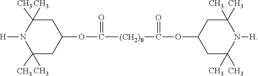
In this instance, the phenol-based antioxidant represented by following Formula 3 is used, and the HALS represent by following Formula 4 is used. In addition, the phenol-based antioxidant is added by 1000 weight ppm with respect to the liquid crystal molecule, and the HALS is added by 250 weight ppm with respect to the liquid crystal molecule.
Figure US09688914-20170627-C00003
Referring to FIG. 5, which is a graph showing an increase of the reliability in an LCD device including a liquid crystal material of the present invention, the voltage holding ratio in the case B and the case C is higher than the case A. Namely, the reliability of the LCD device is improved by the phenol-based antioxidant and by the HALS.
On the other hand, the case D has a similar driving property to the cases A, B and C, while the voltage holding ratio of the case D is rapidly increased after the long-time operation. Namely, as mentioned above, since the phenol-based antioxidant is recycled by the HALS, the reaction between the phenol-based antioxidant and the radicals (or ions) is continuously generated such that the reliability of the LCD device is remarkably increased.
It will be apparent to those skilled in the art that various modifications and variation can be made in the present invention without departing from the spirit or scope of the invention. Thus, it is intended that the present invention cover the modifications and variations of this invention provided they come within the scope of the appended claims and their equivalents.

Claims (2)

What is claimed is:
1. A liquid crystal material, comprising:
a liquid crystal molecule including an alkenyl group;
a phenol-based antioxidant; and
a light stabilizer for recycling the phenol-based antioxidant,
wherein the phenol-based antioxidant is in an amount of 1000 weight ppm with respect to the liquid crystal molecule, and the light stabilizer is in an amount of 250 weight ppm with respect to the liquid crystal molecule,
wherein the phenol-based antioxidant is
Figure US09688914-20170627-C00004
and the light stabilizer is
Figure US09688914-20170627-C00005
2. A liquid crystal display device, comprising:
first and second substrates facing each other;
a pixel electrode on the first substrate;
a common electrode on one of the first and second substrates;
first and second alignment layers respectively over the first and second substrates; and
a liquid crystal layer positioned between the first and second alignment layers, the liquid crystal layer including:
a liquid crystal molecule including an alkenyl group;
a phenol-based antioxidant; and
a light stabilizer for recycling the phenol-based antioxidant,
wherein the phenol-based antioxidant is in an amount of 1000 weight ppm with respect to the liquid crystal molecule and the light stabilizer is in an amount of 250 weight ppm with respect to the liquid crystal molecule, and
wherein the phenol-based antioxidant is
Figure US09688914-20170627-C00006
and the light stabilizer is
Figure US09688914-20170627-C00007
US14/292,514 2013-06-28 2014-05-30 Liquid crystal material and liquid crystal display device including the same Expired - Fee Related US9688914B2 (en)

Applications Claiming Priority (2)

Application Number Priority Date Filing Date Title
KR1020130075528A KR102068961B1 (en) 2013-06-28 2013-06-28 liquid crystal material and liquid crystal display device including the same
KR10-2013-0075528 2013-06-28

Publications (2)

Publication Number Publication Date
US20150002797A1 US20150002797A1 (en) 2015-01-01
US9688914B2 true US9688914B2 (en) 2017-06-27

Family

ID=52115287

Family Applications (1)

Application Number Title Priority Date Filing Date
US14/292,514 Expired - Fee Related US9688914B2 (en) 2013-06-28 2014-05-30 Liquid crystal material and liquid crystal display device including the same

Country Status (3)

Country Link
US (1) US9688914B2 (en)
KR (1) KR102068961B1 (en)
CN (1) CN104250556A (en)

Cited By (1)

* Cited by examiner, † Cited by third party
Publication number Priority date Publication date Assignee Title
US12504568B2 (en) 2020-11-10 2025-12-23 Transitions Optical, Ltd. Photochromic-dichroic articles

Families Citing this family (10)

* Cited by examiner, † Cited by third party
Publication number Priority date Publication date Assignee Title
JP6348600B2 (en) * 2014-08-29 2018-06-27 シャープ株式会社 Liquid crystal display
US10203558B2 (en) 2014-08-29 2019-02-12 Sharp Kabushiki Kaisha Liquid crystal display device
US9783735B2 (en) * 2015-04-15 2017-10-10 Samsung Display Co., Ltd. Liquid crystal display device and liquid crystal composition used therefor
EP3298104B1 (en) * 2015-05-22 2019-03-06 Merck Patent GmbH Liquid-crystalline medium
KR102416574B1 (en) 2015-08-18 2022-07-08 삼성디스플레이 주식회사 Curved liquid crystal display and method for manufacturing the same
CN105504699B (en) * 2015-12-29 2017-08-04 江苏沃特特种材料制造有限公司 Modified liquid-crystal polyester resin compound and preparation method thereof
KR102355529B1 (en) * 2017-08-07 2022-01-26 삼성디스플레이 주식회사 Organic electroluminescence display device
KR102235476B1 (en) 2018-03-30 2021-04-01 주식회사 엘지화학 Liquid crystal alignment composition, method of preparing liquid crystal alignment film, and liquid crystal alignment film using the same
MX2023005404A (en) * 2020-11-10 2023-05-22 Transitions Optical Ltd PHOTOCHROMATIC-DICHROIC ARTICLES.
CN117004409A (en) * 2023-07-31 2023-11-07 河北化工医药职业技术学院 Liquid crystal additive and preparation method, liquid crystal composition, display element and display

Citations (5)

* Cited by examiner, † Cited by third party
Publication number Priority date Publication date Assignee Title
US20070108411A1 (en) * 2005-11-15 2007-05-17 Chisso Corporation Liquid crystal composition and liquid crystal display device
CN101273110A (en) 2005-08-09 2008-09-24 默克专利股份有限公司 liquid crystal medium
US20110101270A1 (en) * 2008-04-22 2011-05-05 Atsutaka Manabe Liquid-crystalline medium
WO2012076105A1 (en) * 2010-12-07 2012-06-14 Merck Patent Gmbh Liquid crystal medium and electrooptic display
WO2012076104A1 (en) * 2010-12-10 2012-06-14 Merck Patent Gmbh Liquid crystal medium and electrooptic display

Family Cites Families (7)

* Cited by examiner, † Cited by third party
Publication number Priority date Publication date Assignee Title
JPH02269189A (en) * 1988-12-06 1990-11-02 Ajinomoto Co Inc Ferroelectric liquid crystal composition and ferroelectric liquid crystal display element
JPH03255423A (en) * 1990-01-12 1991-11-14 Takiron Co Ltd Light control material
EP1184442A1 (en) * 2000-08-30 2002-03-06 Clariant International Ltd. Liquid crystal mixture
CN101880533B (en) * 2004-07-02 2016-05-25 默克专利股份有限公司 Liquid crystal media
TWI369293B (en) * 2004-09-17 2012-08-01 Konica Minolta Opto Inc Polarizing plate protecting film and its manufacturing method, polarizing plate and liquid crystal display
DE102008035890B4 (en) * 2007-08-30 2017-10-19 Merck Patent Gmbh Liquid-crystalline medium and its use
JP5867682B2 (en) * 2011-09-02 2016-02-24 Jsr株式会社 Manufacturing method of liquid crystal display element

Patent Citations (7)

* Cited by examiner, † Cited by third party
Publication number Priority date Publication date Assignee Title
CN101273110A (en) 2005-08-09 2008-09-24 默克专利股份有限公司 liquid crystal medium
US20070108411A1 (en) * 2005-11-15 2007-05-17 Chisso Corporation Liquid crystal composition and liquid crystal display device
US20110101270A1 (en) * 2008-04-22 2011-05-05 Atsutaka Manabe Liquid-crystalline medium
WO2012076105A1 (en) * 2010-12-07 2012-06-14 Merck Patent Gmbh Liquid crystal medium and electrooptic display
US20130248763A1 (en) * 2010-12-07 2013-09-26 Merck Patent Gmbh Liquid-crystalline medium and electro-optical display
WO2012076104A1 (en) * 2010-12-10 2012-06-14 Merck Patent Gmbh Liquid crystal medium and electrooptic display
US20130258268A1 (en) * 2010-12-10 2013-10-03 Merck Patent Gmbh Liquid-crystalline medium and electro-optical display

Cited By (1)

* Cited by examiner, † Cited by third party
Publication number Priority date Publication date Assignee Title
US12504568B2 (en) 2020-11-10 2025-12-23 Transitions Optical, Ltd. Photochromic-dichroic articles

Also Published As

Publication number Publication date
US20150002797A1 (en) 2015-01-01
KR20150002121A (en) 2015-01-07
CN104250556A (en) 2014-12-31
KR102068961B1 (en) 2020-01-22

Similar Documents

Publication Publication Date Title
US9688914B2 (en) Liquid crystal material and liquid crystal display device including the same
US8330919B2 (en) Array substrate for in-plane switching mode liquid crystal display device and method of fabricating the same
US8987746B2 (en) Array substrate for liquid crystal display device
US9310641B2 (en) Display device
US8304039B2 (en) Liquid crystal display device and manufacturing method thereof
US8153208B2 (en) Liquid crystal display, a method for manufacturing a liquid crystal display and a liquid crystal composition
US8003007B2 (en) Liquid crystal composition and liquid crystal display using the same
US20150362788A1 (en) Curved liquid crystal display device
US20080266226A1 (en) Display device
US20090162576A1 (en) Liquid crystal composition and liquid crystal display having the same
US20140267964A1 (en) Liquid crystal driving method and liquid crystal display device
US9360721B2 (en) Liquid crystal display panel
KR102561194B1 (en) Display device
US20140085554A1 (en) Liquid crystal display panel and liquid crystal display device
US8773604B2 (en) Horizontal electric field type liquid crystal display wherein a pixel common electrode is contacted with a common electrode pattern in a non-display pixel area where a width of a gate line narrows
US8228450B2 (en) Liquid crystal display
KR102116943B1 (en) Liquid crystal display device
US20240395828A1 (en) Display device
US20090283204A1 (en) Liquid crystal composition, liquid crystal display having the liquid crystal composition, and manufacturing method of the liquid crystal display
KR102211702B1 (en) Display panel and display apparatus having the same
US10768498B2 (en) Liquid crystal display device
KR102022526B1 (en) Thin Film Transistor Substrate For Flat Panel Display Having Ultra-High Brightness Back Light Unit
KR20070073171A (en) Display substrate and liquid crystal display panel having same
KR101243801B1 (en) Multi-domain liquid crystal display device
WO2021106336A1 (en) Thin-film transistor using oxide semiconductor, and semiconductor device using same

Legal Events

Date Code Title Description
AS Assignment

Owner name: LG DISPLAY CO., LTD., KOREA, REPUBLIC OF

Free format text: ASSIGNMENT OF ASSIGNORS INTEREST;ASSIGNORS:ROH, SEUNG-KWANG;CHOI, WOO-YOUNG;REEL/FRAME:033142/0946

Effective date: 20140409

STCF Information on status: patent grant

Free format text: PATENTED CASE

FEPP Fee payment procedure

Free format text: MAINTENANCE FEE REMINDER MAILED (ORIGINAL EVENT CODE: REM.); ENTITY STATUS OF PATENT OWNER: LARGE ENTITY

LAPS Lapse for failure to pay maintenance fees

Free format text: PATENT EXPIRED FOR FAILURE TO PAY MAINTENANCE FEES (ORIGINAL EVENT CODE: EXP.); ENTITY STATUS OF PATENT OWNER: LARGE ENTITY

STCH Information on status: patent discontinuation

Free format text: PATENT EXPIRED DUE TO NONPAYMENT OF MAINTENANCE FEES UNDER 37 CFR 1.362

FP Lapsed due to failure to pay maintenance fee

Effective date: 20210627