US9658986B2 - Advanced computational processes and methods of using the same - Google Patents
Advanced computational processes and methods of using the same Download PDFInfo
- Publication number
- US9658986B2 US9658986B2 US14/167,253 US201414167253A US9658986B2 US 9658986 B2 US9658986 B2 US 9658986B2 US 201414167253 A US201414167253 A US 201414167253A US 9658986 B2 US9658986 B2 US 9658986B2
- Authority
- US
- United States
- Prior art keywords
- value
- matrix
- unit
- exponent
- elements
- Prior art date
- Legal status (The legal status is an assumption and is not a legal conclusion. Google has not performed a legal analysis and makes no representation as to the accuracy of the status listed.)
- Active, expires
Links
- 238000000034 method Methods 0.000 title claims description 4
- 230000008569 process Effects 0.000 title claims description 3
- 239000011159 matrix material Substances 0.000 claims abstract description 248
- 238000012545 processing Methods 0.000 claims abstract description 172
- 238000007667 floating Methods 0.000 claims abstract description 44
- 238000006243 chemical reaction Methods 0.000 claims abstract description 20
- 238000003672 processing method Methods 0.000 claims description 10
- 238000010586 diagram Methods 0.000 description 34
- 230000000875 corresponding effect Effects 0.000 description 18
- 238000004364 calculation method Methods 0.000 description 12
- 238000010606 normalization Methods 0.000 description 12
- 238000004891 communication Methods 0.000 description 6
- 238000005516 engineering process Methods 0.000 description 4
- 230000006870 function Effects 0.000 description 3
- 230000014509 gene expression Effects 0.000 description 3
- 230000008901 benefit Effects 0.000 description 2
- 230000002708 enhancing effect Effects 0.000 description 2
- 230000004044 response Effects 0.000 description 2
- 230000004075 alteration Effects 0.000 description 1
- 230000015572 biosynthetic process Effects 0.000 description 1
- 230000002596 correlated effect Effects 0.000 description 1
- 230000007774 longterm Effects 0.000 description 1
- 238000004519 manufacturing process Methods 0.000 description 1
- 230000008520 organization Effects 0.000 description 1
- 230000002093 peripheral effect Effects 0.000 description 1
- 230000000717 retained effect Effects 0.000 description 1
- 238000006467 substitution reaction Methods 0.000 description 1
- 238000003786 synthesis reaction Methods 0.000 description 1
- 238000013519 translation Methods 0.000 description 1
Images


Classifications
-
- G—PHYSICS
- G06—COMPUTING; CALCULATING OR COUNTING
- G06F—ELECTRIC DIGITAL DATA PROCESSING
- G06F17/00—Digital computing or data processing equipment or methods, specially adapted for specific functions
- G06F17/10—Complex mathematical operations
- G06F17/16—Matrix or vector computation, e.g. matrix-matrix or matrix-vector multiplication, matrix factorization
-
- G—PHYSICS
- G06—COMPUTING; CALCULATING OR COUNTING
- G06F—ELECTRIC DIGITAL DATA PROCESSING
- G06F9/00—Arrangements for program control, e.g. control units
- G06F9/06—Arrangements for program control, e.g. control units using stored programs, i.e. using an internal store of processing equipment to receive or retain programs
- G06F9/30—Arrangements for executing machine instructions, e.g. instruction decode
- G06F9/30003—Arrangements for executing specific machine instructions
- G06F9/30007—Arrangements for executing specific machine instructions to perform operations on data operands
- G06F9/3001—Arithmetic instructions
- G06F9/30014—Arithmetic instructions with variable precision
-
- G—PHYSICS
- G06—COMPUTING; CALCULATING OR COUNTING
- G06F—ELECTRIC DIGITAL DATA PROCESSING
- G06F9/00—Arrangements for program control, e.g. control units
- G06F9/06—Arrangements for program control, e.g. control units using stored programs, i.e. using an internal store of processing equipment to receive or retain programs
- G06F9/30—Arrangements for executing machine instructions, e.g. instruction decode
- G06F9/30003—Arrangements for executing specific machine instructions
- G06F9/30007—Arrangements for executing specific machine instructions to perform operations on data operands
- G06F9/30032—Movement instructions, e.g. MOVE, SHIFT, ROTATE, SHUFFLE
-
- G—PHYSICS
- G06—COMPUTING; CALCULATING OR COUNTING
- G06F—ELECTRIC DIGITAL DATA PROCESSING
- G06F9/00—Arrangements for program control, e.g. control units
- G06F9/06—Arrangements for program control, e.g. control units using stored programs, i.e. using an internal store of processing equipment to receive or retain programs
- G06F9/30—Arrangements for executing machine instructions, e.g. instruction decode
- G06F9/30003—Arrangements for executing specific machine instructions
- G06F9/30007—Arrangements for executing specific machine instructions to perform operations on data operands
- G06F9/30036—Instructions to perform operations on packed data, e.g. vector, tile or matrix operations
-
- H—ELECTRICITY
- H03—ELECTRONIC CIRCUITRY
- H03M—CODING; DECODING; CODE CONVERSION IN GENERAL
- H03M7/00—Conversion of a code where information is represented by a given sequence or number of digits to a code where the same, similar or subset of information is represented by a different sequence or number of digits
- H03M7/14—Conversion to or from non-weighted codes
- H03M7/24—Conversion to or from floating-point codes
Definitions
- the embodiments discussed herein are related to a data processing apparatus, data processing method, and a computer product.
- a large volume of matrix computation processing can be required in radio communication signal processing, etc.
- the matrix computation accounts for much of the overall computation volume.
- an array processing architecture is suitable for handling such array-type data that require a large volume of matrix computation processing.
- processors that handle array-type data include, for example, single instruction multiple data (SIMD)-system processors and vector-system processors.
- SIMD single instruction multiple data
- the array-type data handled by an instruction set of such processors is an array of scalar values and unit data is the scalar value.
- the circuit scale is made smaller by the instruction set handling only integer values.
- a technology of using only integer arithmetic calculators without using floating-point arithmetic calculators as an arithmetic device and performing a floating decimal point shift calculation includes, for example, a technology of using only integer arithmetic calculators without using floating-point arithmetic calculators as an arithmetic device and performing a floating decimal point shift calculation. Further, for example, another technology generates floating-point number computation (FP) results obtained by performing calculations with respect to the scalar component of vector input that has been dispatched by a scheduler, by plural FP pipelines, and writes the results to an output buffer.
- FP floating-point number computation
- a maximum exponent detecting apparatus detects the maximum exponent of floating decimal point value counts retained in a floating decimal point value register; significand shifting apparatuses shift the significand by a difference of the maximum exponent and each exponent; coding apparatuses perform encoding and perform conversions into integers that retain the relative magnitude of the values.
- significand shifting apparatuses shift the significand by a difference of the maximum exponent and each exponent; coding apparatuses perform encoding and perform conversions into integers that retain the relative magnitude of the values.
- a data processing apparatus includes a computing unit that performs a matrix computation between data streams whose unit data is of a matrix format; a determining unit that for each matrix obtained by the matrix computation by the computing unit, determines based on the value of each element included in the matrix, an exponent value for expressing each element included in the matrix as a floating decimal point value; a converting unit that converts the value of each element into a significand value of the element, according to the exponent value determined by the determining unit; and an output unit that correlates and outputs the exponent value and each matrix after conversion in which the value of each element in the matrix has been converted by the converting unit.
- FIG. 1 is an explanatory diagram of an example of a data processing method according to a first embodiment
- FIG. 2 is a block diagram of a hardware configuration example of a computer system 200 ;
- FIG. 3 is an explanatory diagram of a functional configuration example of a data processing apparatus 100 according to the first embodiment
- FIG. 4 is an explanatory diagram of one example of processing of a determining unit 302 and a converting unit 303 ;
- FIG. 5 is an explanatory diagram of a circuit configuration example of the data processing apparatus 100 ;
- FIG. 6 is an explanatory diagram of a hardware configuration example of the data processing apparatus 100 ;
- FIG. 7 is an explanatory diagram of an internal configuration example of a DMA 604 ;
- FIG. 8 is a flowchart of one example of data processing of the data processing apparatus 100 ;
- FIG. 9 is a flowchart of one example of specific processing of 22 matrix multiplication
- FIG. 10 is a flowchart of one example of specific processing of 22 matrix addition
- FIG. 11 is a flowchart of one example of specific processing of a 22 inverse matrix computation
- FIG. 12 is an explanatory diagram of an application example of the data processing apparatus 100 ;
- FIG. 13 is an explanatory diagram of processing performed by the determining unit 302 and the converting unit 303 of the data processing apparatus 100 according to a second embodiment
- FIG. 14 is an explanatory diagram depicting a circuit configuration example of a shift count generating circuit 1301 according to a first example
- FIG. 15 is an explanatory diagram depicting a circuit configuration example of the shift count generating circuit 1301 according to a second example
- FIGS. 16A and 16B are explanatory diagrams depicting a comparison example of circuit configurations of the shift count generating circuit 1301 ;
- FIG. 17 is an explanatory diagram depicting an example of a circuit configuration of a computing unit 301 ;
- FIG. 18 is an explanatory diagram of a configuration example of a data path (part 1 );
- FIG. 19 is an explanatory diagram of a configuration example of a data path (part 2 );
- FIG. 20 is an explanatory diagram depicting a circuit configuration example of the data processing apparatus 100 according to a third example.
- FIG. 21 is an explanatory diagram depicting an operation example of a UL n-unit data shift count generating circuit in the shift count generating circuit 1301 of a fourth example.
- FIG. 1 is an explanatory diagram of an example of a data processing method according to a first embodiment.
- a data processing apparatus 100 is a computer that performs stream-type processing.
- Stream-type processing is processing of sequentially reading out a series of data (array-type data) from memory, performing computations and sequentially writing a series of computation results to the memory.
- the data processing apparatus 100 has, as an instruction set, a group of instructions for handling unit data.
- Unit data is, for example, matrix-form (or vector-form) data.
- An instruction is, for example, a multiply instruction, an add instruction, an inverse matrix (divide) instruction, etc.
- the data processing apparatus 100 performs the matrix computation processing of array M by allocating for each matrix included in array M, the exponent part of the matrix unit. This suppresses an increase in the circuit scale as compared with the case of treating each value included in array M as a floating decimal point value and further realizes high calculation accuracy as compared with the case of performing the computation after shifting array M as a whole at a time by an integer shift instruction.
- the computer system 200 is, for example, a smartphone, a cell-phone, a tablet personal computer (PC), a personal handy-phone system (PHS), etc.
- FIG. 2 is a block diagram of a hardware configuration example of a computer system 200 .
- the computer system 200 includes a central processing unit (CPU) 201 , memory 202 , and an interface (I/F) 203 , respectively connected by a bus 210 .
- CPU central processing unit
- I/F interface
- the CPU 201 governs overall control of the computer system 200 .
- the memory 202 includes, for example, read-only memory (ROM), random access memory (RAM), and flash ROM.
- ROM read-only memory
- RAM random access memory
- flash ROM stores programs such as an OS and firmware
- ROM stores application programs
- RAM is used as a work area of the CPU 201 .
- Programs stored in the memory 202 are loaded on the CPU 201 and encoded processes are executed by the CPU 201 .
- the I/F 203 controls the input and output of data with respect to other apparatuses.
- the I/F 203 is connected via a communication line to a network such as a local area network (LAN), a wide area network (WAN), and the Internet; and through the network is connected to other apparatuses.
- the I/F 203 administers an internal interface with the network and controls the input and output of data with respect to other apparatuses.
- the computer system 200 may further include a magnetic disk drive, a magnetic disk, a display, a keyboard, a mouse, etc.
- FIG. 3 is an explanatory diagram of a functional configuration example of the data processing apparatus 100 according to the first embodiment.
- the data processing apparatus 100 is configured to include a computing unit 301 , a determining unit 302 , a converting unit 303 , and an output unit 304 .
- each functional unit may be formed by elements such as an AND as a logical AND circuit, an inverter as a negative logic circuit, an OR as a logical OR circuit, a NOR as a logical NOR circuit, and a flip-flop (FF) as a latch circuit.
- FF flip-flop
- Each functional unit may be implemented by a field programmable gate array (FPGA), with the function being defined by description in, for example, Verilog-hardware description language (HDL), etc., and with the logic synthesis performed of the description.
- Functions of each functional unit may be implemented, for example, by causing the CPU 201 to execute a program stored in the memory 202 depicted in FIG. 2 , or by the I/F 203 .
- the computing unit 301 performs a matrix computation between data streams D.
- a data stream D is array-type data whose unit data are of a matrix format.
- a matrix computation is, for example, matrix multiplication, matrix addition, inverse matrix (matrix division), etc.
- the value of each element of the matrix included in a data stream D is, for example, the integer value.
- two data streams D subject to computation will occasionally be described as “source (0)” and “source (1)”.
- the computing unit 301 sequentially performs the matrix computation of matrices included in source (0) and matrices included in source (1), from the head matrix to the end matrix of each source. It is noted, however, that the number of data streams D subject to computation may be three or more.
- the determining unit 302 determines, based on the value of each element included in the matrix, the exponent value of the matrix unit in the case of expressing each element as a floating decimal point value.
- the exponent value is the value of the exponent part in the case of expressing each element as a floating decimal point value.
- the determining unit 302 may determine, as the exponent value of the matrix unit, the exponent value in the case of expressing, as a floating decimal point value, the element whose absolute value is the greatest among plural elements included in the matrix, for each of the matrices to be obtained by the matrix computation of the computing unit 301 .
- the determining unit 302 identifies the element whose absolute value is the greatest among plural elements included in the matrix. The determining unit 302 then normalizes the value of the element whose absolute value is the greatest to calculate the significand value and the exponent value.
- the significand value is the value of the significand part in the case of expressing the element as a floating decimal point value.
- the determining unit 302 determines the exponent value of the element whose absolute value is the greatest to be the exponent value of the matrix unit. Namely, the determining unit 302 unifies the exponent values in the case of expressing the elements included in the matrix as a floating decimal point value, for each matrix. Specific processing of the determining unit 302 will be described later with reference to FIG. 4 .
- the converting unit 303 converts the value of each element included in the matrix into the significand value of each element according to the exponent value of the matrix unit determined by the determining unit 302 .
- the converting unit 303 converts the value of each element included in the matrix to the value shifted by the exponent value of the matrix unit (significand value). Specific processing of the converting unit 303 will be described later with reference to FIG. 4 .
- the output unit 304 correlates and outputs the matrix after the conversion in which the value of each element has been converted by the converting unit 303 , and the exponent value of the matrix unit determined by the determining unit 302 .
- the output unit 304 correlates and sequentially writes to memory (e.g., a data memory 606 depicted in FIG. 6 to be described later), the matrix after the conversion in which the value of each element included in the matrix has been converted, and the exponent value of the matrix unit.
- the array of the matrices after the conversion in which the value of each element included in the matrix has been converted by the converting unit 303 (hereinafter, occasionally described as “significand part stream”) and the array of the exponent values of the matrix unit determined by the determining unit 302 (hereinafter, occasionally described as “exponent part stream”) are output.
- the computing unit 301 may perform the matrix computation of the data stream D including the significand part stream and the exponent part stream output by the output unit 304 .
- the computing unit 301 performs the matrix multiplication of two significand part streams and performs vector addition of two exponent part streams.
- the computing unit 301 performs the matrix addition computation between two data streams D by shifting the value of each element included in one of the corresponding matrices between the two data streams D, based on a difference of corresponding exponent values between the two data streams D.
- the exponent values of the matrices subject computation it becomes possible to cause the exponent values of the matrices subject computation to match.
- the converting unit 303 may convert the value of each element included in the matrix to the significand value of each element according to the exponent value of each data stream D unit.
- the exponent value for the data stream D unit is arbitrarily settable, for example, as an immediate source operand of an instruction.
- the converting unit 303 converts the value of each element included in the matrix into the value shifted by the exponent value of the data stream D unit.
- the output unit 304 may correlate and output the matrix after the conversion in which the value of each element included in the matrix has been converted by the converting unit 303 , and the exponent value of the data stream D unit.
- the exponent value of the data stream D unit will occasionally be described as “shift count S”.
- FIG. 4 is an explanatory diagram of one example of processing of the determining unit 302 and the converting unit 303 .
- source (0) is the array-type data whose unit data is of the matrix format.
- a[0] to a[L] are values of the elements of the matrix included in source (0).
- a[0] denotes the value of the first row and first column, a[1] the first row and second column, a[2] the second row and first column, and a[3] the second row and second column.
- Source (1) is array-type data whose unit data is of the matrix format.
- b[0] to b[M] are values of the elements of the matrix included in source (1).
- a computation result 400 is a matrix representing the result of the matrix computation of the matrix included in source (0) and the matrix included in source (1).
- c[0] to c[N] are the values of the elements included in the computation result 400 .
- a correspondence relationship of the computation of the elements due to differences of L, M, and N is determined by the kind of instruction.
- the determining unit 302 identifies the element whose absolute value is the greatest among plural elements included in the computation result 400 .
- the determining unit 302 then normalizes the value of the element whose absolute value is the greatest to calculate the significand value and the exponent value.
- the determining unit 302 determines, as the exponent value of the matrix unit, the exponent value of the element whose absolute value is the greatest. In the following description, the exponent value of the matrix unit will occasionally be described as “shift count s”.
- the converting unit 303 performs a computation for shifting the value of each element included in the computation result 400 by shift count s determined by the determining unit 302 and calculates the significand values c′[0] to c′[N] of the elements.
- the value of each of c′[0] to c′[N] is the integer value of w bits.
- the converting unit 303 converts the values of the elements included in the computation result 400 to the calculated significand values c′[0] to c′[N] of the elements.
- the output unit 304 correlates and outputs the computation result 400 after the conversion including the significand values c′[0] to c′[N] of the elements, and shift count s.
- the significand part stream 410 and the exponent part stream 420 can be output.
- FIG. 5 is an explanatory diagram of a circuit configuration example of the data processing apparatus 100 .
- the data processing apparatus 100 has an computing device group 501 , a stream unit block shift unit 502 , and a data unit block normalizing unit 503 .
- the computing device group 501 performs the matrix computation of source (0) and source (1).
- Stream data Z is an array that results from the matrix computation between source (0) and source (1).
- the computing device group 501 corresponds to, for example, the computing unit 301 depicted in FIG. 3 .
- the data processing apparatus 100 has two modes, including a DCLSS mode-on and a DCLSS mode-off.
- the DCLSS mode-on is the mode at which the integer stream is input and the significand part stream and the exponent part stream are output.
- the DCLSS mode-off is the mode at which the integer stream is input and the integer stream is output.
- a user can arbitrarily select any one among the DCLSS mode-on and the DCLSS mode-off. For example, in the case of performing the matrix multiplication or the matrix division between two data streams D, since it is highly likely that the number of bits required for expressing the computation result will increase once, the user selects the DCLSS mode-on. In the case of performing the matrix addition between two data streams D, since it is unlikely that the number of bits required for expressing the computation result will increase once, the user selects the DCLSS mode-off.
- the stream unit block shift unit 502 performs the computation of shifting the value of each element included in matrix Z[22] by shift count S, for each matrix Z[22] included in the stream data Z.
- the [22] denotes two rows by two columns.
- the stream unit block shift unit 502 then converts the value of each element included in matrix Z[22] to the 16-bit integer value.
- Matrix Z[22] after conversion to the 16-bit integer value is described as matrix F[22].
- the stream unit block shift unit 502 corresponds to, for example, the converting unit 303 depicted in FIG. 3 .
- processing of shifting the value of each element included in the matrix by the shift count S and converting the value of each element included in the matrix to the 16-bit integer value will occasionally be described as “stream unit block shift processing”.
- the data unit block normalizing unit 503 When the DCLSS mode-on is selected, the data unit block normalizing unit 503 performs the data unit block normalization processing for each matrix Z[22] included in the stream data Z.
- the data unit block normalizing unit 503 corresponds to, for example, the determining unit 302 and the converting unit 303 depicted in FIG. 3 .
- matrix Z[22] can be expressed, for example, by equation (1).
- Matrix F[22] after the conversion in which the values of the elements Z′ 0 , Z 1 , Z′ 2 , and Z′ 3 included in matrix Z′[22] have been converted to the significand, values corresponding to the exponent value e 1 becomes as indicated by equation (3).
- Exponent value E of the matrix unit corresponding to matrix F[22] becomes as indicated by equation (4).
- the values of the elements Z 0 to Z 3 included in matrix Z[22] are 32-bit integer values as indicated below.
- significand part stream of source (0) will occasionally be described as “significand part stream (0)” and the exponent part stream of source (0) will occasionally be described as “exponent part stream (0)”.
- the significand part stream of source (1) will occasionally be described as “significand part stream (1)” and the exponent part stream of source (1) will occasionally be described as “exponent part stream (1)”.
- the computing unit 301 performs the vector addition of the exponent part stream (0) and the exponent part stream (1), using equation (6), where A_e[i] is the i-th data included in the exponent part stream (0) and B_e[i] is the i-th data included in the exponent part stream (1).
- tmp_e1[i] is the i-th computation result.
- tmp _ e 1 [i] A _ e[i]+B _ e[i] (6)
- the computing unit 301 then calculates the i-th computation result of the exponent part of the 22 matrix multiplication of source (0) and source (1), using the following equation (7).
- Z _ e[i] tmp _ e 0 [i]+tmp _ e 1 [i] (7)
- the computing unit 301 calculates the i-th computation result of the exponent part of the 22 matrix addition between source (0) and source (1), using equation (11).
- Z _ e[i ] ( A _ e[i] ⁇ B _ e[i ])? B _ e[i]:A _ e[i] (11)
- the computing unit 301 performs the inverse matrix computation for the i-th data included in the significand part stream (0), using equation (12).
- Z _ f[i],tmp _ e 0 [i ]) Inverse( A _ f[i ]) (12)
- the arithmetic part 301 calculates the i-th computation result of the exponent part of the 22 inverse matrix computation of source (0), using equation (13).
- Z _ e[i] tmp _ e 0 [i]+A _ e[i] (13)
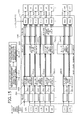
- FIG. 6 is an explanatory diagram of a hardware configuration example of the data processing apparatus 100 .
- the data processing apparatus 100 includes the stream unit block shift unit 502 , the data unit block normalizing unit 503 , an instruction decoder 601 , an arithmetic data path 602 , a multiplexer (MUX) 603 , a direct memory access (DMA) 604 , instruction memory 605 , and data memory 606 .
- MUX multiplexer
- DMA direct memory access
- the instruction decoder 601 decodes the contents of an instruction read into the instruction memory 605 and outputs a DMA control signal to the DMA 604 as well as outputs a data path control signal to the arithmetic data path 602 .
- the DMA control signal includes an operand indicative of an object of the computation and a destination indicative of a storage location of the computation result.
- the data path control signal includes the computation code indicative of the type of the instruction.
- the DMA control signal includes src0, src1, dst, and SL.
- src0 is the address in the data memory 606 at which source (0) is stored.
- src1 is the address in the data memory 606 at which source (1) is stored.
- dst is the address at which the computation result is stored in the data memory 606 .
- SL is the stream length.
- the data path control signal includes mxmul indicative of the multiply instruction.
- the arithmetic data path 602 performs various types of matrix computations by switching internal wire connections by a control circuit (not depicted), in response to the data path control signal from the instruction decoder 601 .
- the arithmetic data path 602 has eight 2 ⁇ 2 matrix multiplication modules and eight 2 ⁇ 2 matrix addition modules and each set of four modules has one multiplexer attached thereto.
- the arithmetic data path 602 can perform the 4 ⁇ 4 matrix multiplication, four 2 ⁇ 2 matrix multiplications in parallel, four 2 ⁇ 2 inverse matrix computations in parallel, etc., by switching the wire connections between the modules.
- DMA 604 reads out the source from the data memory 606 and transfers the source to the arithmetic data path 602 , in response to the DMA control signal from the instruction decoder 601 .
- the DMA 604 writes to the storage location (destination) of the data memory 606 , the computation results to be output from the MUX 603 .
- the stream unit block shift unit 502 performs the stream unit block shift processing for the computation result from the arithmetic data path 602 .
- the data unit block normalizing unit 503 performs the data unit block normalization processing for the computation result from the arithmetic data path 602 .
- the MUX 603 outputs to the DMA 604 , the computation result to be output from the stream unit block shift unit 502 or the data unit block normalizing unit 503 , according to the DCLSS mode.
- FIG. 7 is an explanatory diagram of an internal configuration example of the DMA 604 .
- addr_src0 denotes the address at which source (0) is stored
- addr_src1 the address at which source (1) is stored
- addr_dst the destination address the address at which source (0) is stored
- length_src0 denotes the stream length SL of source (0)
- length_src1 the stream length SL of source (1)
- length_dst the stream length SL of the destination.
- the DMA 604 includes, for example, a loading unit 710 that reads out source (0), a loading unit 720 that reads out source (1), a storing unit 730 that writes the data to the destination, and a cycle counter 740 .
- the loading unit 710 includes an address generating circuit 711 and a data buffer 712 .
- addr_src0 and length_src0 are input to the address generating circuit 711 .
- the address generating circuit 711 reads out one unit data each cycle, from the address specified by addr_src0 of the data memory 606 and stores the unit data to the data buffer 712 .
- the unit data is a type of data that is treated as an object of computation by the arithmetic data path 602 and for example, the matrix, numerical value, etc., are specified.
- the data stored in the data buffer 712 is output to the arithmetic data path 602 to become the object of computation, as necessary.
- the loading unit 720 includes an address generating circuit 721 and a data buffer 722 .
- addr_src1 and length_src1 are input to the address generating circuit 721 .
- the address generating circuit 721 reads out one unit data each cycle, from the address specified by addr_src1 of the data memory 606 and stores the unit data to the data buffer 722 .
- the data stored in the data buffer 722 is output to the arithmetic data path 602 to become the object of computation, as necessary.
- the storing unit 730 includes an address generating circuit 731 and a data buffer 732 .
- addr_dst and length_dst are input to the address generating circuit 731 .
- the address generating circuit 731 writes one unit data stored in the data buffer 732 each cycle to the address specified by addr_dst of the data memory 606 .
- the data buffer 732 stores the computation result output from the MUX 603 .
- FIG. 8 is a flowchart of one example of the data processing of the data processing apparatus 100 .
- the data processing apparatus 100 reads in the instruction from the instruction memory 605 (step S 801 ).
- the data processing apparatus 100 sets the shift count S of the stream unit in the stream unit block shift unit 502 and sets the DCLSS mode in the MUX 603 (step S 802 ).
- the data processing apparatus 100 transmits a DMA control signal to the DMA 604 and transmits a data path control signal to the arithmetic data path 602 (step S 803 ).
- the data processing apparatus 100 increments “i” (step S 810 ) and determines whether “i” is less than “SL” (step S 811 ). If “i” is less than “SL” (step S 811 : YES), then the data processing apparatus 100 goes back to step S 805 . On the other hand, if “i” is greater than or equal to “SL” (step S 811 : NO), then the data processing apparatus 100 ends the sequence of processing based on this flowchart.
- the floating decimal point by the matrix unit by allocating the exponent value of the matrix unit, for each matrix included in the array-type data, at the time of the DCLSS mode-on. Further, it possible to express the floating decimal point by the array-type data unit, by shifting the array-type data as a whole at a time by the integer shift instruction, at the time of the DCLSS mode-off.
- FIG. 9 is a flowchart of one example of specific processing of the 22 matrix multiplication.
- the data processing apparatus 100 performs the matrix multiplication of the significand part stream (0) and the significand part stream (1), using equation (5) above (step S 901 ).
- the data processing apparatus 100 then performs the vector addition of the exponent part stream (0) and the exponent part stream (1), using equation (6) above (step S 902 ).
- the data processing apparatus 100 calculates the i-th computation result of the exponent part of the 22 matrix multiplication of source (0) and source (1), using equation (7) above (step S 903 ).
- the data processing apparatus 100 outputs the i-th computation result (Z_f[i],Z_e[i]) of the 22 matrix multiplication of source (0) and source (1) (step S 904 ), ending a sequence of processing based on this flowchart.
- Z_f[i],Z_e[i] the 22 matrix multiplication of source (0) and source (1)
- FIG. 10 is a flowchart of one example of specific processing of the 22 matrix addition.
- the data processing apparatus 100 performs the vector subtraction of the exponent part stream (0) and the exponent part stream (1), using equation (8) above (step S 1001 ).
- the data processing apparatus 100 determines if tmp_e0[i] is greater than or equal to 0 (step S 1002 ).
- step S 1002 If tmp_e0[i] is greater than or equal to 0 (step S 1002 : YES), then the data processing apparatus 100 performs the 22 matrix addition with shifting, using equation (9) above (step S 1003 ). On the other hand, if tmp_e0[i] is not greater than or equal to 0 (step S 1002 : NO), then the data processing apparatus 100 performs the 22 matrix addition with shifting, using equation (10) above (step S 1004 ).
- the data processing apparatus 100 calculates the i-th computation result of the exponent part of the 22 matrix addition of source (0) and source (1), using equation (11) above (step S 1005 ).
- the data processing apparatus 100 then outputs the i-th computation results (Z_f[i],Z_e[i]) of the 22 matrix addition of source (0) and source (1) (step S 1006 ), ending a sequence of processing based on this flowchart.
- FIG. 11 is a flowchart of one example of specific processing of the 22 inverse matrix computation.
- the data processing apparatus 100 performs inverse matrix computation of the i-th data included in the significand part stream (0), using equation (12) above (step S 1101 ).
- the data processing apparatus 100 calculates the i-th computation result of the exponent part of the 22 inverse matrix computation of source (0), using equation (13) above (step S 1102 ). The data processing apparatus 100 then outputs the i-th computation result (Z_f[i],Z_e[i]) of the 22 inverse matrix computation of source (0) (step S 1103 ), ending a sequence of processing based on this flowchart. Thus, it possible to perform the 22 inverse matrix computation of source (0).
- FIG. 12 is an explanatory diagram of an application example of the data processing apparatus 100 .
- a baseband processing LSI 1200 includes a radio frequency (RF) unit 1210 , dedicated hardware 1220 , digital signal processors (DSPs) 1230 #1 to 1230 #3.
- RF radio frequency
- DSPs digital signal processors
- the RF unit 1210 down-converts the frequency of a radio signal received by way of an antenna 1250 , converts the radio signal to a digital signal, and outputs the resulting signal to a bus 1240 .
- the RF unit 1210 converts the digital signal output to the bus 1240 to an analog signal, up-converts the analog signal to the radio frequency, and outputs the resulting signal to the antenna 1250 .
- the dedicated hardware 1220 includes, for example, a turbo to handle error-correcting code, a Viterbi to execute Viterbi algorithm, a multiple input/multiple output (MIMO) to transmit and receive data by plural antennas, etc.
- a turbo to handle error-correcting code
- a Viterbi to execute Viterbi algorithm
- MIMO multiple input/multiple output
- Each of the DSPs 1230 #1 to 1230 #3 includes a processor 1231 , program memory 1232 , a peripheral circuit 1233 , and data memory 1234 .
- the processor 1231 includes a CPU 1235 and the data processing apparatus 100 . Processing elements of the radio communication signal processing, such as a searcher (synchronization), a demodulator (demodulation), a decoder (decoding), a codec (encoding), and a modulator (modulation), are allocated to the DSPs 1230 .
- the data processing apparatus 100 can determine for each matrix to be obtained by the matrix computation of a data stream D, the exponent value of the matrix unit in the case of expressing each element in as a floating decimal point value, based on the value of each element included in the matrix.
- the data processing apparatus 100 can convert the value of each element included in the matrix to the significand value of each element corresponding to the exponent value of the matrix unit and, correlate and output the matrix after the conversion and the exponent value of the matrix unit.
- the array-type data whose unit data is a matrix has the characteristics that while the values of the elements included in one matrix are approximate to one another as absolute values, the values of the elements between the matrices differ widely as absolute values. For this reason, with the matrix computation performed by allocating the exponent value of the matrix unit for each matrix included in the array-type data, the calculation accuracy can be enhanced efficiently.
- the data processing apparatus 100 can determine for each matrix to be obtained by the matrix computation of the stream data D, the exponent value in the case of expressing as a floating decimal point value, the element whose absolute value is the greatest among plural elements included in the matrix as the exponent value of the matrix unit. Thus, it is possible to unify and normalize the exponent parts of all elements included in the matrix by the exponent part of the element whose absolute value is the greatest, thereby enhancing the calculation accuracy.
- the data processing apparatus 100 can calculate the difference of the corresponding exponent values between the two data streams D.
- the data processing apparatus 100 can shift the value of each element included in either one of the corresponding matrices between the two data streams D, based on the difference of the corresponding exponent values between the two data streams D. This makes it possible to cause the exponent values of the matrices subject to computation to match, enabling the matrix addition computation of the two data streams D.
- the data processing apparatus 100 can arbitrarily select the DCLSS mode. This makes it possible to select the DCLSS mode-on in the case of performing matrix computation that is highly likely to increase the number of bits required to express the computation result at a time and select the DCLSS mode-off in other cases, suppressing the amount of processing required for the matrix computation.
- the data processing apparatus, the data processing method, and the data processing program according to the first embodiment can suppress increases in circuit scale related to the matrix computation of the array-type data as well as enhance the calculation accuracy.
- the data processing apparatus 100 according to a second embodiment will be described. Components identical to those of the first embodiment are given the same reference numerals used in the first embodiment and description thereof is omitted hereinafter.
- the unit data length is the length of a unit of a matrix format (or vector format) data and is, for example, represented by the number of elements included in the unit of data.
- the unit data length may be denoted as “unit data length UL”.
- the unit data length UL is fixed as (N+1) elements (c[0] to c[N]) per cycle.
- the unit data length UL changes according to the issued instruction. Consequently, with the unit data length UL changing for each instruction, the SIMD width (parallelism) changes.
- the data processing width per cycle is regarded as “the data processing width L (fixed)”, where the SIMD width is “L/UL”.
- the data processing width L is determined according to the hardware resources of the data processing apparatus 100 and is the data width that can be processed in 1 cycle.
- the SIMD width is the number of unit data that can be processed in parallel per cycle.
- the unit data length UL is 16 and the SIMD width is 1 SIMD, i.e., 16 elements of 1 data/cycle.
- the unit data length UL is 4 and the SIMD width is 4 SIMD, i.e., 4 elements of 4 data/cycle.
- a data processing method will be described that can be implemented by logic that is as simple as possible for determining the data unit exponent value when each element included in 1 unit data is expressed as a floating decimal point value and for performing normalization processing of data unit blocks to convert the value of each element into a significand value according to the exponent value of the data unit even when the unit data length UL is variable.
- FIG. 13 is an explanatory diagram of processing performed by the determining unit 302 and the converting unit 303 of the data processing apparatus 100 according to the second embodiment.
- a shift count generating circuit 1301 is a determining circuit of the determining unit 302 .
- a shifter 1302 is a shifting circuit of the converting unit 303 .
- the shift count generating circuit 1301 determines for each element set of the element count unit, which is the unit data length UL, the exponent value of the element set. For example, based on the value of each element included in an element set, the shift count generating circuit 1301 determines the exponent value for the element set when the elements are expressed by a floating decimal point value.
- the shift count generating circuit 1301 determines for each element set of 4 units, which is the unit data length UL, the exponent value of the element set.
- the shift count generating circuit 1301 identifies the element having the greatest absolute value among the element set c[0] to c[3].
- the shift count generating circuit 1301 normalizes the value of the element having the greatest absolute value and calculates the significand value and the exponent value.
- the shift count generating circuit 1301 determines the exponent value of the element having the greatest absolute value to be the element set shift count s.
- the shift counts s0 to s3 of the elements c[0] to c[3] are the same shift count s(s0).
- the shift count generating circuit 1301 determines the exponent value obtained by normalizing the value of the element having the greatest absolute value among the element set c[4] to c[7] to be the element set shift count s. In other words, the shift counts s4 to s7 of the elements c[4] to c[7] are the same shift count s.
- the shift count generating circuit 1301 determines the exponent value obtained by normalizing the value of the element having the greatest absolute value among the element set c[8] to c[11] to be the element set shift count s. In other words, the shift counts s8 to s11 are the same shift count s.
- the shift count generating circuit 1301 determines the exponent value obtained by normalizing the value of the element having the greatest absolute value among the element set c[12] to c[15] as the element set shift count s. In other words, the shift counts s12 to s15 of the elements c[12] to c[15] is the same shift count s.
- the shifter 1302 for each element set of an element count unit that is the unit data length UL, converts the value of each element included in the element set, into the significand value of the element according to the element set shift count s determined by the shift count generating circuit 1301 .
- the shifter 1302 shifts the value of each element by the shift counts s4 to s7, performs a computation with respect to each value, and calculates the significand value c′[4] to c′[7] of each element.
- the shifter 1302 converts the value of each element into the calculated significand value c′[4] to c′[7] of each element.
- the shifter 1302 shifts the value of each element by the shift values s8 to s11, performs a computation with respect to each value, and calculates the significand value c′[8] to c′[11] of each element.
- the shifter 1302 converts the value of each element into the calculated significand value c′[8] to c′[11] of each element.
- the shifter 1302 shifts the value of each element by the shift counts s12 to s15, performs a computation with respect to each value, and calculates the significand value c′[12] to c′[15] of each element.
- the shifter 1302 converts the value of each element into the calculated significand value c′[12] to c′[15] of each element.
- the output unit 304 correlates and outputs the series of resulting converted elements c′[0] to c′[15] and the shift counts s0 to s15.
- the output unit 304 correlates the element shift count s with each element set of the element count unit that is the unit data length UL, among the series of resulting converted elements c′[0] to c′[15].
- the element set shift count s can be determined to express, as a floating decimal point value, each element included in the element set. Further, according to the data processing apparatus 100 , for each element set, the value of each element included in the element set can be converted into the significand value of the element according to the element set shift count s. According to the data processing apparatus 100 , the value of each element included in the post-conversion element set and the element set shift count s can be correlated and output.
- a data unit exponent value can be assigned according to the variable unit data length UL and expressed as a floating decimal point value for each data unit.
- the series of elements (array-type data) obtained by the matrix computation by the computing unit 301 is assumed to be elements c[0] to c[15].
- FIG. 14 is an explanatory diagram depicting a circuit configuration example of the shift count generating circuit 1301 according to the first example.
- the shift count generating circuit 1301 includes UL n-unit data shift count generating circuits 1401 to 1416 and MUXs 1421 to 1436 .
- the MUXs 1421 to 1436 are selecting circuits corresponding to the elements c[0] to c[15].
- the elements included in an element set are 1 element.
- the UL 1-unit data shift count generating circuit 1401 - 1 receives input of the value of the element c[0], normalizes the value of the element c[0], calculates the significand value and the exponent value, and determines the calculated exponent value to be the element set shift count s (shift count s0).
- the determined shift count s0 is input to the MUX 1421 .
- the UL 1-unit data shift count generating circuits 1401 - 2 to 1401 - 16 determine element set shift counts s (shift counts s1 to s15). Further, the determined shift counts s1 to s15 are input into the MUXs 1422 to 1436 , respectively.
- the UL 2-unit data shift count generating circuit 1402 - 1 receives input of the elements c[0], c[1], normalizes the value of the element having the greatest absolute value among the element set c[0], c[1]; and calculates the significand value and the exponent value.
- the determined shift counts s0, s1 are input into the MUX 1421 , 1422 , respectively.
- the MUXs 1421 to 1436 from among the input element set shift counts s, selects the element set shift count s that is for an element set that of an element count equivalent to the unit data length UL, for each of the elements included among the elements c[0] to c[15].
- the element count that is the unit data length UL is input to the MUXs 1421 to 1436 .
- the MUX 1421 selects as the element set shift count s, the shift counts s0 input by the UL 1-unit data shift count generating circuit 1401 - 1 .
- the shift counts s (shift counts s0 to s15) selected by the MUXs 1421 to 1436 are input into the shifter 1302 depicted in FIG. 13 .
- the shifter 1302 converts the value of each of the element c[0] to c[15] into the significand value c′[0] to c′[15] with respect to the shift counts s respectively selected by the MUXs 1421 to 1436 .
- the data processing apparatus 100 according to a second example will be described.
- FIG. 15 is an explanatory diagram depicting a circuit configuration example of the shift count generating circuit 1301 according to a second example.
- the shift count generating circuit 1301 further includes MUXs 1511 to 1526 corresponding to the elements c[0] to c[15].
- the elements included in the element set are 1 element.
- the MUXs 1511 to 1526 from among the respectively input element set shift counts s, selects the element set shift count s that is for an element count that is equivalent to the unit data length UL.
- the element count that is equivalent to the unit data length UL is input into the MUX 1511 to 1526 .
- the MUX 1511 selects, as the element set shift count s, the shift counts s0 input by the UL 2-unit data shift count generating circuit 1502 - 1 .
- the MUX 511 selects, as the element set shift count s, the shift counts s0 input by the UL 4-unit data shift count generating circuit 1503 - 1 .
- the shift counts s (shift counts s0 to s15) respectively selected by the MUXs 1511 to 1526 are input into the shifter 1302 depicted in FIG. 13 .
- the shifter 1302 converts the value of each of the elements c[0] to c[15] into the significand value c′[0] to c′[15] with respect to the shift counts s respectively selected by the MUXs 1511 to 1526 .
- the circuit volume of the shift count generating circuit 1301 can be suppressed.
- circuit configurations of the shift count generating circuit 1301 according to the first example and of the shift count generating circuit 1301 according to the second example will be compared.
- FIGS. 16A and 16B are explanatory diagrams depicting a comparison example of the circuit configurations of the shift count generating circuit 1301 .
- FIG. 16A depicts an example of a circuit configuration of the shift count generating circuit 1301 (see FIG. 14 ) of the first example.
- FIG. 16B depicts an example of a circuit configuration of the shift count generating circuit 1301 (see FIG. 15 ) of the second example.
- the UL n-unit data shift count generating circuits are limited to a power of 2 and therefore, there may be cases where a UL n-unit data shift count generating circuit corresponding to the unit data length UL is not present.
- a UL n-unit data shift count generating circuit corresponding to the unit data length UL is not present.
- a UL n-unit data shift count generating circuit corresponding to the unit data length UL is not present.
- FIG. 17 is an explanatory diagram depicting an example of a circuit configuration of the computing unit 301 .
- the computing unit 301 includes MUXs 1701 to 1716 , and computing devices 1721 to 1728 .
- the MUX 1701 is a selecting circuit that receives input of source (0), selects an element from source (0) according to an instruction, and outputs the selected element to the computing device 1721 .
- the MUXs 1703 , 1705 , 1707 , 1709 , 1711 , 1713 , and 1715 are selecting circuits that receive input of source (0), select an element from source (0) according to an instruction, and output the selected element to the computing devices 1722 to 1728 , respectively.
- the MUX 1702 is a selecting circuit that receives input of source (1), selects an element from source (1) according to an instruction, and outputs the selected element to the computing device 1721 .
- the MUXs 1704 , 1706 , 1708 , 1710 , 1712 , 1714 , and 1716 are selecting circuits that receive input of source (1), select an element from source (1) according to an instruction, and output the selected element to the computing devices 1722 to 1728 , respectively.
- the computing device 1721 multiples the elements respectively input by the MUXs 1701 , 1702 ; and outputs the computation result c[0].
- the computing devices 1722 to 1728 multiply the input elements, and output computation results c[1] to c[7], respectively.
- FIG. 18 is an explanatory diagram of a configuration example of a data path (part 1 ).
- 4 elements a[0] to a[3] are respectively input into the computing devices 1721 to 1724 ; and from the head of source (1), 4 elements b[0] to b[3] are respectively input into the computing devices 1721 to 1724 .
- the computing devices 1721 to 1724 perform multiplication with respect to the elements, and output the computation results c[0] to c[3].
- the subsequent 4 elements a[4] to a[7] of source (0) are respectively input into the computing devices 1725 to 1728 ; and the subsequent 4 elements b[4] to b[7] of source (1) are input into the computing devices 1725 to 1728 .
- the computing devices 1725 to 1728 perform multiplication with respect to the elements and output the computation results c[4] to c[7].
- FIG. 19 is an explanatory diagram of a configuration example of a data path (part 2 ).
- a UL 3-unit data shift count generating circuit that corresponds to the unit data length UL is not present in the shift count generating circuit 1301 .
- the shift count generating circuit 1301 uses the UL 4-unit data shift count generating circuit 1503 (see FIG. 15 ) that corresponds to an element count of 4, which is greater than the unit data length UL of 3, and determines the element set shift count s.
- the shift count generating circuit 1301 selects elements from source (0) and source (1), and performs computations such that the elements are aligned as powers of 2 at the MUXs 1701 to 1716 that are at the input side of the computing devices 1721 to 1724 .
- the 3 elements a[0] to a[2] are respectively input into the computing devices 1721 to 1723 ; and from the head of source (1), the 3 elements b[0] to b[2] are respectively input into the computing devices 1721 to 1723 .
- the computing devices 1721 to 1723 perform multiplication with respect to the elements, and output the computation results c[0] to c[2].
- the subsequent 3 elements a[3] to a[5] of source (0) are respectively input into the computing devices 1725 to 1727 ; and the subsequent 3 elements b[3] to b[5] of source (1) are respectively input into the computing devices 1725 to 1727 .
- the computing devices 1725 to 1727 perform multiplication with respect to the elements, and output the computation results c[3] to c[5].
- the shift count generating circuit 1301 when performing computation selects from source (0) and source (1), elements such that from the head, the fourth and the eighth computing devices 1724 and 1728 are skipped.
- the UL n-unit data shift count generating circuit that corresponds to an element count that is greater than the unit data length UL
- the UL n-unit data shift count generating circuit into which the elements are to be input can be suitably adjusted.
- normalization processing can be implemented with respect to a data unit block that corresponds to the unit data length UL.
- the SIMD width does not decrease easily and drops in the processing performance of the data processing apparatus 100 can be suppressed.
- the UL n-unit data shift count generating circuits are limited to powers of 2, configuration is not limited hereto.
- the UL n-unit data shift count generating circuits may be limited to a count other than 2 (e.g., 3 ) with the data processing width L as an upper limit, or may be limited to an odd or even element count n.
- the data processing apparatus 100 according to a third example will be described.
- the third example to suppress the circuit volume of the data processing apparatus 100 , a case where the shifter 1302 is shared by a DCLSS mode-on and a DCLSS mode-off.
- FIG. 20 is an explanatory diagram depicting a circuit configuration example of the data processing apparatus 100 according to the third example.
- the data processing apparatus 100 includes the shift count generating circuit 1301 , the shifter 1302 , and MUXs 2001 to 2016 .
- FIG. 20 a portion of the circuit configuration of the data processing apparatus 100 is depicted.
- the shift count generating circuit 1301 receives input of the elements c[0] to c[15], determines the shift counts s of the elements c[0] to c[15], and outputs the shift counts s determined for the element c[0] to c[15] to the corresponding MUXs 2001 to 2016 , respectively.
- the MUXs 2001 to 2016 are selecting circuits that correspond to the elements c[0] to c[15].
- the MUX 2001 receives input of the shift counts s for the element c[0] and the shift count S for the data stream unit, and outputs to the shifter 1302 , as the shift count s0 for the element c[0] according to the DCLSS mode, any one among the shift count s and the shift count S.
- the MUX 2001 outputs the shift count s to the shifter 1302 .
- the MUX 2001 outputs the shift count S to the shifter 1302 .
- the DCLSS mode is set, for example, by the instruction decoder 601 depicted in FIG. 6 .
- the MUXs 2002 to 2016 receive input of the shift counts s for the elements c[1] to c[15] and the shift count S, and output to the shifter 1302 , as the shift counts s1 to s15 for the elements c[1] to c[15] according to the DCLSS mode, any one among the shift counts s and the shift count S.
- the shifter 1302 receives input of the elements c[0] to c[15] and the shift counts s0 to s15, and converts the value of the elements c[0] to c[15] into the significand value c′[0] to c′[15] according to the shift counts s0 to s15.
- the shifter 1302 for each element set of an element count unit that is the unit data length UL, converts the value of each element included in the element set into a significand value according to the element set shift counts s determined by the shift count generating circuit 1301 .
- the shifter 1302 converts the value of each element among the elements c[0] to c[15] into a significand value according to the shift count S.
- the element set shift counts s are the shift counts s respectively selected by the MUXs 1421 to 1436 of the shift count generating circuit 1301 depicted in FIG. 14 and the MUXs 1511 to 1526 of the shift count generating circuit 1301 depicted in FIG. 15 .
- the shifter 1302 can be shared through the DCLSS mode-on and the DCLSS mode-off. Consequently, the DCLSS mode that receives an integer stream as input and outputs the significand part stream and the exponent part stream can be implemented while suppressing increases in circuit volume.
- the data processing apparatus 100 will be described.
- the shift count generating circuit 1301 will be described that can output suitable element set shift counts s and exponent value s0 to s15 for the elements c[0] to c[15] even when the elements included among the elements c[0] to c[15] are expressed as floating decimal point values and not integers.
- the shift count generating circuit 1301 determines as the element set shift count s, the exponent value s_max, which is the greatest exponent value among the exponent values e of the elements included in the element set.
- the shifter 1302 for each element set, converts the significand value f of each element included in the element set, into the significand value of the elements for the exponent value resulting after subtracting the exponent values e of the elements from the exponent value s_max.
- FIG. 21 An operation example of the shift count generating circuit 1301 will be described with reference to FIG. 21 .
- the UL 3-unit data shift count generating circuit 1403 - 1 (see FIG. 14 ) will be described as an example.
- FIG. 21 is an explanatory diagram depicting an operation example of a UL n-unit data shift count generating circuit in the shift count generating circuit 1301 of the fourth example.
- c[0] to c[2] are expressed by floating decimal point values having the significand value f and the exponent value e.
- c[ 0] ( f 0 ,e 0)
- c[ 1] ( f 1 ,e 1)
- c[ 2] ( f 2 ,e 2)
- the UL 3-unit data shift count generating circuit 1403 - 1 uses expression (17) below, and identifies the exponent value s_max, which is greatest among the input exponent value e0 to e2 of the elements c[0] to c[2].
- s _max max( e 0 ,e 1 ,e 2) (17)
- the UL 3-unit data shift count generating circuit 1403 - 1 determines as the element set shift count s, and outputs the identified exponent value s_max. Further, the UL 3-unit data shift count generating circuit 1403 - 1 , for example, uses expression (18) to (20) below; calculates the exponent values s0 to s2 of the elements c[0] to c[2] by subtracting the exponent values e0 to e2 of the elements c[0] to c[2] from the exponent value s_max; and outputs the exponent values s0 to s2 of the elements c[0] to c[2] to the shifter 1302 .
- s 0 s _max- e 0 (18)
- s 1 s _max ⁇ e 1 (19)
- s 2 s _max ⁇ e 2 (20)
- a suitable element set shift count s (s_max) and suitable exponent values s0 to s2 of the elements c[0] to c[2] can be output.
- the shifter 1302 converts the significand values f0 to f2 of the elements c[0] to c[2] into the significand values c′[0] to c′[2] of each element according to the input exponent values s0 to s2.
- the UL 3-unit data shift count generating circuit 1403 - 1 in the shift count generating circuit 1301 has been described as an example, the other UL n-unit data shift count generating circuits (see FIGS. 14 and 15 ) perform similar operation.
- the element set shift count s that is the unit data length UL and the exponent values s0 to s15 of the elements c[0] to c[15] can be output.
- normalization processing can be performed with respect to data unit blocks that correspond to the unit data length UL.
- the data processing method described in the present embodiment may be implemented by executing a prepared program on a computer such as a personal computer and a workstation.
- the program is stored on a non-transitory, computer-readable recording medium such as a hard disk, a flexible disk, a CD-ROM, an MO, and a DVD, read out from the computer-readable medium, and executed by the computer.
- the program may be distributed through a network such as the Internet.
- the data processing apparatus 100 described in the present embodiment can be realized by an application specific integrated circuit (ASIC) such as a standard cell or a structured ASIC, or a programmable logic device (PLD) such as a field-programmable gate array (FPGA).
- ASIC application specific integrated circuit
- PLD programmable logic device
- FPGA field-programmable gate array
- functional units are defined in hardware description language (HDL), which is logically synthesized and applied to the ASIC, the PLD, etc., thereby enabling manufacture of the data processing apparatus 100 .
- HDL hardware description language
- the embodiments enable increases in circuit scale to be suppressed while enhancing calculation accuracy.
Abstract
Description
(Z_f[i],tmp_e0[i])=A_f[i]*B_f[i] (5)
tmp_e1[i]=A_e[i]+B_e[i] (6)
Z_e[i]=tmp_e0[i]+tmp_e1[i] (7)
tmp_e0[i]=B_e[i]−A_e[i] (8)
Z_f[i]=A_f[i]>>tmp_e0[i]+B_f[i] (9)
Z_f[i]=A_f[i]+B_f[i]>>tmp_e0[i] (10)
Z_e[i]=(A_e[i]<B_e[i])?B_e[i]:A_e[i] (11)
(Z_f[i],tmp_e0[i])=Inverse(A_f[i]) (12)
Z_e[i]=tmp_e0[i]+A_e[i] (13)
c[0]=(f0,e0) (14)
c[1]=(f1,e1) (15)
c[2]=(f2,e2) (16)
s_max=max(e0,e1,e2) (17)
s0=s_max-e0 (18)
s1=s_max−e1 (19)
s2=s_max−e2 (20)
Claims (11)
Applications Claiming Priority (4)
| Application Number | Priority Date | Filing Date | Title |
|---|---|---|---|
| JP2013029464 | 2013-02-18 | ||
| JP2013-029464 | 2013-02-18 | ||
| JP2013-257371 | 2013-12-12 | ||
| JP2013257371A JP6225687B2 (en) | 2013-02-18 | 2013-12-12 | Data processing apparatus and data processing method |
Publications (2)
| Publication Number | Publication Date |
|---|---|
| US20140237010A1 US20140237010A1 (en) | 2014-08-21 |
| US9658986B2 true US9658986B2 (en) | 2017-05-23 |
Family
ID=51352083
Family Applications (1)
| Application Number | Title | Priority Date | Filing Date |
|---|---|---|---|
| US14/167,253 Active 2035-09-09 US9658986B2 (en) | 2013-02-18 | 2014-01-29 | Advanced computational processes and methods of using the same |
Country Status (2)
| Country | Link |
|---|---|
| US (1) | US9658986B2 (en) |
| JP (1) | JP6225687B2 (en) |
Cited By (5)
| Publication number | Priority date | Publication date | Assignee | Title |
|---|---|---|---|---|
| US10346163B2 (en) * | 2017-11-01 | 2019-07-09 | Apple Inc. | Matrix computation engine |
| US10642620B2 (en) | 2018-04-05 | 2020-05-05 | Apple Inc. | Computation engine with strided dot product |
| US10754649B2 (en) | 2018-07-24 | 2020-08-25 | Apple Inc. | Computation engine that operates in matrix and vector modes |
| US10831488B1 (en) | 2018-08-20 | 2020-11-10 | Apple Inc. | Computation engine with extract instructions to minimize memory access |
| US10970078B2 (en) | 2018-04-05 | 2021-04-06 | Apple Inc. | Computation engine with upsize/interleave and downsize/deinterleave options |
Families Citing this family (6)
| Publication number | Priority date | Publication date | Assignee | Title |
|---|---|---|---|---|
| US10419501B2 (en) * | 2015-12-03 | 2019-09-17 | Futurewei Technologies, Inc. | Data streaming unit and method for operating the data streaming unit |
| US9965187B2 (en) * | 2016-02-18 | 2018-05-08 | Lawrence Livermore National Security, Llc | Near-memory data reorganization engine |
| CN107315715B (en) * | 2016-04-26 | 2020-11-03 | 中科寒武纪科技股份有限公司 | Apparatus and method for performing matrix addition/subtraction operation |
| CN107941256B (en) * | 2017-11-20 | 2020-03-06 | 中国电子科技集团公司第四十一研究所 | Numerical value personalized display method of high-precision measuring instrument |
| US11307860B1 (en) | 2019-11-22 | 2022-04-19 | Blaize, Inc. | Iterating group sum of multiple accumulate operations |
| US10996960B1 (en) * | 2019-11-22 | 2021-05-04 | Blaize, Inc. | Iterating single instruction, multiple-data (SIMD) instructions |
Citations (8)
| Publication number | Priority date | Publication date | Assignee | Title |
|---|---|---|---|---|
| JPH08101919A (en) | 1994-09-30 | 1996-04-16 | Sony Corp | Numerical converter and device for turning coordinate value to integer |
| JP2005031848A (en) | 2003-07-09 | 2005-02-03 | Sony Corp | Method, program, and device for floating point arithmetic operation |
| US20070074009A1 (en) | 2005-09-28 | 2007-03-29 | Donofrio David D | Scalable parallel pipeline floating-point unit for vector processing |
| US20090292750A1 (en) * | 2008-05-22 | 2009-11-26 | Videolq, Inc. | Methods and apparatus for automatic accuracy- sustaining scaling of block-floating-point operands |
| US20110099295A1 (en) * | 2009-10-23 | 2011-04-28 | Samplify Systems, Inc. | Block floating point compression of signal data |
| US20110302231A1 (en) * | 2010-06-02 | 2011-12-08 | Maxeler Technologies, Ltd. | Method and apparatus for performing numerical calculations |
| US20130262539A1 (en) * | 2012-03-30 | 2013-10-03 | Samplify Systems, Inc. | Conversion and compression of floating-point and integer data |
| US20130262548A1 (en) * | 2012-03-27 | 2013-10-03 | Fujitsu Semiconductor Limited | Matrix calculation unit |
Family Cites Families (4)
| Publication number | Priority date | Publication date | Assignee | Title |
|---|---|---|---|---|
| JPH0784753A (en) * | 1993-09-20 | 1995-03-31 | Fujitsu Ltd | Fixed point type digital signal processor |
| DE19826252C2 (en) * | 1998-06-15 | 2001-04-05 | Systemonic Ag | Digital signal processing method |
| JP2002215384A (en) * | 2001-01-16 | 2002-08-02 | Toshiba Corp | Multi-input addition and subtraction circuit |
| JP5811175B2 (en) * | 2011-05-16 | 2015-11-11 | 日本電気株式会社 | Arithmetic processing device and arithmetic processing method |
-
2013
- 2013-12-12 JP JP2013257371A patent/JP6225687B2/en not_active Expired - Fee Related
-
2014
- 2014-01-29 US US14/167,253 patent/US9658986B2/en active Active
Patent Citations (9)
| Publication number | Priority date | Publication date | Assignee | Title |
|---|---|---|---|---|
| JPH08101919A (en) | 1994-09-30 | 1996-04-16 | Sony Corp | Numerical converter and device for turning coordinate value to integer |
| JP2005031848A (en) | 2003-07-09 | 2005-02-03 | Sony Corp | Method, program, and device for floating point arithmetic operation |
| US20070074009A1 (en) | 2005-09-28 | 2007-03-29 | Donofrio David D | Scalable parallel pipeline floating-point unit for vector processing |
| JP2009505301A (en) | 2005-09-28 | 2009-02-05 | インテル・コーポレーション | Scalable parallel pipelined floating point unit for vector processing |
| US20090292750A1 (en) * | 2008-05-22 | 2009-11-26 | Videolq, Inc. | Methods and apparatus for automatic accuracy- sustaining scaling of block-floating-point operands |
| US20110099295A1 (en) * | 2009-10-23 | 2011-04-28 | Samplify Systems, Inc. | Block floating point compression of signal data |
| US20110302231A1 (en) * | 2010-06-02 | 2011-12-08 | Maxeler Technologies, Ltd. | Method and apparatus for performing numerical calculations |
| US20130262548A1 (en) * | 2012-03-27 | 2013-10-03 | Fujitsu Semiconductor Limited | Matrix calculation unit |
| US20130262539A1 (en) * | 2012-03-30 | 2013-10-03 | Samplify Systems, Inc. | Conversion and compression of floating-point and integer data |
Cited By (9)
| Publication number | Priority date | Publication date | Assignee | Title |
|---|---|---|---|---|
| US10346163B2 (en) * | 2017-11-01 | 2019-07-09 | Apple Inc. | Matrix computation engine |
| US10592239B2 (en) | 2017-11-01 | 2020-03-17 | Apple Inc. | Matrix computation engine |
| US10877754B2 (en) | 2017-11-01 | 2020-12-29 | Apple Inc. | Matrix computation engine |
| US10642620B2 (en) | 2018-04-05 | 2020-05-05 | Apple Inc. | Computation engine with strided dot product |
| US10970078B2 (en) | 2018-04-05 | 2021-04-06 | Apple Inc. | Computation engine with upsize/interleave and downsize/deinterleave options |
| US10990401B2 (en) | 2018-04-05 | 2021-04-27 | Apple Inc. | Computation engine with strided dot product |
| US10754649B2 (en) | 2018-07-24 | 2020-08-25 | Apple Inc. | Computation engine that operates in matrix and vector modes |
| US11042373B2 (en) | 2018-07-24 | 2021-06-22 | Apple Inc. | Computation engine that operates in matrix and vector modes |
| US10831488B1 (en) | 2018-08-20 | 2020-11-10 | Apple Inc. | Computation engine with extract instructions to minimize memory access |
Also Published As
| Publication number | Publication date |
|---|---|
| JP2014179065A (en) | 2014-09-25 |
| JP6225687B2 (en) | 2017-11-08 |
| US20140237010A1 (en) | 2014-08-21 |
Similar Documents
| Publication | Publication Date | Title |
|---|---|---|
| US9658986B2 (en) | Advanced computational processes and methods of using the same | |
| Umuroglu et al. | Bismo: A scalable bit-serial matrix multiplication overlay for reconfigurable computing | |
| US10474627B2 (en) | Neural network unit with neural memory and array of neural processing units that collectively shift row of data received from neural memory | |
| US7797366B2 (en) | Power-efficient sign extension for booth multiplication methods and systems | |
| CN114868108A (en) | Systolic array component combining multiple integer and floating point data types | |
| US8631380B2 (en) | Method of, and apparatus for, data path optimisation in parallel pipelined hardware | |
| US9436465B2 (en) | Moving average processing in processor and processor | |
| JP2013541084A (en) | Method and apparatus for performing floating point division | |
| US20150106414A1 (en) | System and method for improved fractional binary to fractional residue converter and multipler | |
| Choi et al. | Energy-efficient design of processing element for convolutional neural network | |
| CN105335127A (en) | Scalar operation unit structure supporting floating-point division method in GPDSP | |
| US11647227B2 (en) | Efficient transforms and transposes for rate-distortion optimization and reconstruction in video encoders | |
| US20200097253A1 (en) | Digital Circuit With Compressed Carry | |
| US8140608B1 (en) | Pipelined integer division using floating-point reciprocal | |
| Kuang et al. | Energy-efficient multiple-precision floating-point multiplier for embedded applications | |
| US20040117421A1 (en) | Methods and systems for computing floating-point intervals | |
| EP1984810B1 (en) | A booth multiplier with enhanced reduction tree circuitry | |
| US20220365755A1 (en) | Performing constant modulo arithmetic | |
| Aizaz et al. | State-of-art analysis of multiplier designs for image processing and convolutional neural network applications | |
| US20220156567A1 (en) | Neural network processing unit for hybrid and mixed precision computing | |
| US8938485B1 (en) | Integer division using floating-point reciprocal | |
| Savadi et al. | A survey on design of digital signal processor | |
| US8924447B2 (en) | Double precision approximation of a single precision operation | |
| Ueno et al. | Parameterized design and evaluation of bandwidth compressor for floating-point data streams in FPGA-based custom computing | |
| Gilani et al. | Virtual floating-point units for low-power embedded processors |
Legal Events
| Date | Code | Title | Description |
|---|---|---|---|
| AS | Assignment |
Owner name: FUJITSU SEMICONDUCTOR LIMITED, JAPAN Free format text: ASSIGNMENT OF ASSIGNORS INTEREST;ASSIGNORS:GE, YI;KOBAYASHI, NOBURO;HATANO, HIROSHI;AND OTHERS;REEL/FRAME:032102/0648 Effective date: 20140110 Owner name: FUJITSU LIMITED, JAPAN Free format text: ASSIGNMENT OF ASSIGNORS INTEREST;ASSIGNORS:GE, YI;KOBAYASHI, NOBURO;HATANO, HIROSHI;AND OTHERS;REEL/FRAME:032102/0648 Effective date: 20140110 |
|
| AS | Assignment |
Owner name: FUJITSU LIMITED, JAPAN Free format text: CORRECTIVE ASSIGNMENT TO CORRECT THE SECOND INVENTOR'S NAME PREVIOUSLY RECORDED ON REEL 032102 FRAME 0648. ASSIGNOR(S) HEREBY CONFIRMS THE EXECUTED ASSIGNMENT;ASSIGNORS:GE, YI;KOBAYASHI, NOBORU;HATANO, HIROSHI;AND OTHERS;REEL/FRAME:032435/0013 Effective date: 20140110 Owner name: FUJITSU SEMICONDUCTOR LIMITED, JAPAN Free format text: CORRECTIVE ASSIGNMENT TO CORRECT THE SECOND INVENTOR'S NAME PREVIOUSLY RECORDED ON REEL 032102 FRAME 0648. ASSIGNOR(S) HEREBY CONFIRMS THE EXECUTED ASSIGNMENT;ASSIGNORS:GE, YI;KOBAYASHI, NOBORU;HATANO, HIROSHI;AND OTHERS;REEL/FRAME:032435/0013 Effective date: 20140110 |
|
| AS | Assignment |
Owner name: FUJITSU LIMITED, JAPAN Free format text: ASSIGNMENT OF ASSIGNORS INTEREST;ASSIGNORS:FUJITSU LIMITED;FUJITSU SEMICONDUCTOR LIMITED;REEL/FRAME:035481/0271 Effective date: 20150302 Owner name: SOCIONEXT INC., JAPAN Free format text: ASSIGNMENT OF ASSIGNORS INTEREST;ASSIGNORS:FUJITSU LIMITED;FUJITSU SEMICONDUCTOR LIMITED;REEL/FRAME:035481/0271 Effective date: 20150302 |
|
| AS | Assignment |
Owner name: FUJITSU LIMITED, JAPAN Free format text: ASSIGNMENT OF ASSIGNORS INTEREST;ASSIGNOR:SOCIONEXT, INC.;REEL/FRAME:039318/0020 Effective date: 20160617 |
|
| STCF | Information on status: patent grant |
Free format text: PATENTED CASE |
|
| MAFP | Maintenance fee payment |
Free format text: PAYMENT OF MAINTENANCE FEE, 4TH YEAR, LARGE ENTITY (ORIGINAL EVENT CODE: M1551); ENTITY STATUS OF PATENT OWNER: LARGE ENTITY Year of fee payment: 4 |