US9658630B2 - Digital filter and timing signal generation circuit - Google Patents
Digital filter and timing signal generation circuit Download PDFInfo
- Publication number
- US9658630B2 US9658630B2 US14/634,354 US201514634354A US9658630B2 US 9658630 B2 US9658630 B2 US 9658630B2 US 201514634354 A US201514634354 A US 201514634354A US 9658630 B2 US9658630 B2 US 9658630B2
- Authority
- US
- United States
- Prior art keywords
- value
- minimum
- output
- measurement
- maximum
- Prior art date
- Legal status (The legal status is an assumption and is not a legal conclusion. Google has not performed a legal analysis and makes no representation as to the accuracy of the status listed.)
- Expired - Fee Related
Links
Images


Classifications
-
- G—PHYSICS
- G05—CONTROLLING; REGULATING
- G05F—SYSTEMS FOR REGULATING ELECTRIC OR MAGNETIC VARIABLES
- G05F1/00—Automatic systems in which deviations of an electric quantity from one or more predetermined values are detected at the output of the system and fed back to a device within the system to restore the detected quantity to its predetermined value or values, i.e. retroactive systems
- G05F1/10—Regulating voltage or current
- G05F1/46—Regulating voltage or current wherein the variable actually regulated by the final control device is DC
Definitions
- the embodiments discussed herein are related to a digital filter and a timing signal generation circuit.
- semiconductor integrated circuits have been widely used in various devices such as electronic devices.
- the semiconductor integrated circuits such as processors consume power, for example, when executing a computing operation.
- the power consumed by the semiconductor integrated circuit varies depending on, for example, the computing operation performed at that time. For example, also in the clock gating technique for decreasing power consumption, the consumed power considerably varies between clock-disabled time and clock-enabled time.
- clock frequency control is known in which voltage fluctuations are tracked to modulate a clock frequency.
- delay deterioration attributable to the voltage fluctuations is tracked to lower the clock frequency, and the timing constraint violation is thereby avoided.
- Examples of proposed technologies in the related art include a technology by which delay variation in a semiconductor element is compensated for in such a manner that supply voltage fluctuations are detected.
- Another example of proposed clock frequency control methods in the related art is a method by which a change in the oscillation frequency of a ring oscillator is converted into a delay variation value to modulate, based on the amount of correction for the delay variation, a clock frequency of a phase locked loop (PLL).
- PLL phase locked loop
- the method employs feedforward control, it takes time to measure the oscillation frequency of the ring oscillator, and thus only delay variation attributable to low-frequency voltage fluctuations is addressed.
- Another example of the proposed clock frequency control is a method by which, based on setup slack (setup constraint margin) measured by a critical path monitor, a clock frequency of a PLL is modulated to control an amount of setup slack.
- a semiconductor integrated circuit (package containing a semiconductor chip) has a resonance frequency of, for example, tens of MHz to hundreds of MHz, and thus the voltage at a sudden consumed-current increase fluctuates in a band from tens of MHz to hundreds of MHz.
- the control is not performed in time for delay variation in the resonance frequency band of the semiconductor integrated circuit package. It is thus difficult to fully compensate for the delay variation.
- the frequency modulation does not track the voltage fluctuations, and thus the frequency is undesirably lowered. In other words, it is difficult to avoid a disadvantage of the clock frequency control, in voltage fluctuations in a particular frequency band.
- a digital filter includes: a minimum-value holder that holds a minimum value of a measurement value inputted in the minimum-value holder and that outputs the minimum value as a held value; a limit-value circuit that receives the held value and that outputs the held value as a limit value in a case where the held value remains minimum during predetermined cycles; and an output controller that receives a maximum value, the measurement value, and the limit value, the maximum value defining an upper limit, outputs the measurement value as an output value if the measurement value is smaller than the limit value, and outputs the maximum value as the output value if the measurement value is equal to or larger than the limit value.
- FIG. 1 is a graph illustrating an impedance characteristic of a power-supply network of a processor
- FIG. 2 is a graph for explaining first droop noise in the impedance characteristic illustrated in FIG. 1 ;
- FIG. 3 is a diagram (1/3) for explaining clock frequency control on the first droop noise
- FIGS. 4A and 4B are graphs (2/3) for explaining the clock frequency control on the first droop noise
- FIGS. 5A and 5B are graphs (3/3) for explaining the clock frequency control on the first droop noise
- FIG. 6 is a diagram (1/3) for explaining the clock frequency control performed in a case of simultaneous switching noise superposition
- FIGS. 7A and 7B are graphs (2/3) for explaining the clock frequency control performed in the case of simultaneous switching noise superposition
- FIGS. 8A and 8B are graphs (3/3) for explaining the clock frequency control performed in the case of simultaneous switching noise superposition
- FIG. 9 is a block diagram illustrating a digital filter according to a first embodiment
- FIG. 10 is a block diagram illustrating an example of a minimum-value holder in the digital filter illustrated in FIG. 9 ;
- FIG. 11 is a time chart for explaining an example of operation of the digital filter illustrated in FIG. 9 ;
- FIG. 12 is a time chart for explaining another example of the operation of the digital filter illustrated in FIG. 9 ;
- FIG. 13 is a time chart for explaining yet another example of the operation of the digital filter illustrated in FIG. 9 ;
- FIG. 14 is a time chart for explaining yet another example of the operation of the digital filter illustrated in FIG. 9 ;
- FIG. 15 is a graph illustrating a simulation result in the operation of the digital filter illustrated in FIG. 9 ;
- FIG. 16 is a diagram (1/3) for explaining clock frequency control performed in a case where the digital filter according to the first embodiment removes simultaneous switching noise;
- FIGS. 17A and 17B are graphs (2/3) for explaining the clock frequency control performed in the case where the digital filter according to the first embodiment removes the simultaneous switching noise;
- FIGS. 18A and 18B are graphs (3/3) for explaining the clock frequency control performed in the case where the digital filter according to the first embodiment removes the simultaneous switching noise;
- FIG. 19 is a block diagram illustrating a digital filter according to a second embodiment
- FIG. 20 is a time chart for explaining an example of operation of the digital filter illustrated in FIG. 19 ;
- FIG. 21 is a graph illustrating a simulation result in the operation of the digital filter illustrated in FIG. 19 ;
- FIG. 22 is a block diagram illustrating a digital filter according to a third embodiment
- FIG. 23 is a time chart for explaining an example of operation of the digital filter illustrated in FIG. 22 ;
- FIG. 24 is a graph illustrating a simulation result in the operation of the digital filter illustrated in FIG. 22 ;
- FIG. 25 is a block diagram illustrating a digital filter according to a fourth embodiment
- FIG. 26 is a block diagram illustrating a digital filter according to a fifth embodiment
- FIG. 27 is a block diagram illustrating a digital filter according to a sixth embodiment
- FIG. 28 is a block diagram illustrating a digital filter according to a seventh embodiment
- FIG. 29 is a block diagram illustrating a digital filter according to an eighth embodiment.
- FIG. 30 is a diagram (1/3) for explaining clock frequency control performed in a case where the digital filter according to the eighth embodiment removes simultaneous switching noise;
- FIGS. 31A and 31B are graphs (2/3) for explaining the clock frequency control performed in the case where the digital filter according to the eighth embodiment removes the simultaneous switching noise.
- FIGS. 32A and 32B are graphs (3/3) for explaining the clock frequency control performed in the case where the digital filter according to the eighth embodiment removes the simultaneous switching noise.
- timing signal generation circuit Before describing in detail a digital filter, a timing signal generation circuit, and a semiconductor integrated circuit according to embodiments discussed herein, examples of and issues regarding the timing signal generation circuit and the semiconductor integrated circuit will first be described with reference to FIGS. 1 to 8B .
- FIG. 1 is a graph illustrating an impedance characteristic of a processor of a power-supply network.
- FIG. 2 is a graph for explaining first droop noise in the impedance characteristic illustrated in FIG. 1 .
- the horizontal axis represents frequency, while the vertical axis represents magnitude of a relative impedance.
- a resonance frequency of a package of a semiconductor integrated circuit is tens of MHz to hundreds of MHz. Accordingly, a voltage fluctuation band observed in sudden consumed-current increase is also tens of MHz to hundreds of MHz, as illustrated in FIG. 1 .
- a first droop region (first droop noise) where the relative impedance increases is present around, for example, 150 MHz.
- the presence of the first droop region is attributed to, for example, a power supply wiring pattern in a silicon chip, wiring for connecting a terminal of a silicon chip and an external terminal of a package, or the like. This defines a resonance frequency of the package.
- noise in a frequency band (second droop region) from approximately 1 MHz to approximately ten of MHz is also present, the noise being attributed to, for example, mounting a semiconductor integrated circuit on a substrate.
- vibrations in the frequency band that is the aforementioned first droop region are observed at locations (timings) of 50 nsec and 200 nsec at which the load current changes.
- the load current in the processor changes in the same manner as the consumed power. This causes di/dt noise, for example, at timings of 50 nsec and 200 nsec, and thus causes voltage fluctuations in the power supply wiring and the ground wiring in the semiconductor integrated circuit.
- a ground voltage drop and a ground voltage bounce occur at the timing of 50 nsec when the load current increases, and that a supply voltage bounce and a ground voltage drop occur at the timing of 200 nsec when the consumed current decreases.
- the voltage and current fluctuations end with a potential (for example, 0.95V) of the supply voltage and a potential (for example, 0V) of the ground voltage after a certain time has elapsed.
- the semiconductor element of the semiconductor integrated circuit operates in accordance with an operating voltage using a potential difference between the power supply and the ground.
- the semiconductor element operates fast at a high operating voltage, and operates slowly at a low operating voltage. Accordingly, an occurrence of voltage fluctuations attributable to the consumed current leads to a variation in the speed of the semiconductor element (hereinafter, the speed variation of the semiconductor element is also referred to as delay variation).
- timing constraint violation (setup violation)
- clock frequency control adaptive frequency/supply tracking: adaptive clock-frequency control
- voltage fluctuations are tracked to modulate a clock frequency.
- delay deterioration attributable to the voltage fluctuations is tracked to lower the clock frequency, and the timing constraint violation is thereby avoided.
- Another example of proposed clock frequency control methods is a method by which a change in the oscillation frequency of a ring oscillator is converted into a delay variation value to modulate, based on the amount of correction for the delay variation, a clock frequency of a PLL.
- FIGS. 3 to 5B are a diagram and graphs for explaining the clock frequency control of the first droop noise, and illustrate effects on the timing, the effects being obtained by applying the clock frequency control to the power supply noise (first droop noise) described with reference to FIG. 2 .
- a control delay is denoted by Td
- a voltage-fluctuation frequency power supply noise: first droop noise
- Fns voltage-fluctuation frequency
- Tns cycle of the power supply noise
- FIG. 3 illustrates an example of the semiconductor integrated circuit including a semiconductor chip 100 .
- the semiconductor chip 100 includes a timing-signal generation circuit 1 , a clock tree 3 , and a data path 4 .
- the timing-signal generation circuit 1 generates a timing signal (clock CLK), and includes a voltage-fluctuation observer 11 and a PLL 2 .
- the PLL 2 includes a loop filter 21 , a gain normalizer 22 , a digital controlled oscillator (DCO) 23 , a divider 24 , a subtractor 25 , and an adder 26 .
- DCO digital controlled oscillator
- the subtractor 25 subtracts the phase of output from the divider 24 from the phase of output from a reference signal REF received from outside, and outputs the result to the loop filter 21 .
- the loop filter 21 cuts off undesirable short-cycle fluctuations from the output from the subtractor 25 , and outputs the result to the gain normalizer 22 .
- the gain normalizer 22 receives the output from the loop filter 21 , and normalizes (Fref/Kdco) the output, where Fref is a frequency of the reference signal REF, and Kdco is a gain of the DCO 23 .
- the gain normalizer 22 then outputs the result to the adder 26 .
- the adder 26 adds up the output from the gain normalizer 22 and the output from the voltage-fluctuation observer 11 , and outputs the result to the DCO 23 .
- the DCO 23 outputs, to the clock tree 3 , an oscillation signal having the frequency based on the output from the adder 26 as output (a clock) CLK from the timing-signal generation circuit 1 , while feeding back the oscillation signal to the divider 24 .
- the clock tree 3 supplies circuits of the semiconductor integrated circuit with the clock CLK, for example, as a clock for a clock terminal of a flip-flop in the data path 4 , through a plurality of buffers arranged in a tree.
- the PLL 2 , the clock tree 3 , and the data path 4 illustrated in FIG. 3 are merely examples. It goes without saying that various variations and modifications may be made to the configuration.
- FIG. 4A illustrates an input voltage (Vns) of the voltage-fluctuation observer 11
- FIG. 4B illustrates an output code (measurement value Vfo) of the voltage-fluctuation observer 11 .
- the horizontal axis represents time (nsec)
- the vertical axis represents voltage (V).
- the horizontal axis represents time (nsec)
- the vertical axis represents output code.
- FIGS. 5A and 5B are provided for explaining the clock frequency control of the first droop noise.
- FIG. 5A illustrate a case where the clock frequency control is not performed.
- FIG. 5B illustrates a case where the clock frequency control is performed.
- the horizontal axis represents time (nsec)
- the vertical axis represents setup slack (psec).
- a low-pass filter is provided at an input end of the voltage-fluctuation observer 11 , or a moving-average filter, a finite impulse response (FIR) filter, or the like is provided at an output end of the voltage-fluctuation observer 11 .
- FIR finite impulse response
- the clock frequency control in the case where the clock frequency control is performed on the first droop noise, the clock frequency control enables the setup slack to be improved and thus to avoid the occurrence of the timing constraint violation.
- the voltage-fluctuation observer 11 has a considerable delay in the voltage fluctuation observation, so that a control delay is increased.
- a clock latency is also added to the process time. This also increases the control delay.
- FIGS. 6 to 8B are a diagram and graphs for explaining the clock frequency control performed in a case of simultaneous switching noise superposition, and illustrate effects exerted by the clock frequency control performed when a digital filter according to any one of the embodiments (described later) is not used.
- FIG. 6 illustrates a semiconductor integrated circuit (the semiconductor chip 100 ) having the same configuration as the aforementioned configuration in FIG. 3 .
- FIGS. 7A and 7B correspond to FIGS. 4A and 4B described above, and FIGS. 8A and 8B correspond to FIGS. 5A and 5B described above.
- the clock frequency control if the clock frequency control is performed on the first droop noise in the case of simultaneous switching noise superposition, the clock frequency control thereby enables the setup slack to be improved and thus to avoid the occurrence of the timing constraint violation.
- another example of the proposed clock frequency control methods is a method by which, based on setup slack measured by a critical path monitor, a clock frequency of a PLL is modulated to control an amount of setup slack.
- this method employs feedback control, and thus has a late response when a disturbance factor is to be addressed. Accordingly, only delay variation attributable to low-frequency voltage fluctuations is addressed.
- the semiconductor integrated circuit package has the resonance frequency of, for example, tens of MHz to hundreds of MHz, and thus the voltage at a sudden consumed-current increase fluctuates in a band from tens of MHz to hundreds of MHz.
- the control is not performed in time for the delay variation in the resonance frequency band of the semiconductor integrated circuit package. It is thus difficult to fully compensate for the delay variation.
- the control delay is not reduced to zero.
- the feedforward control is performed in a period from detecting the voltage fluctuations that are a disturbance factor of the delay variation to applying the oscillation-frequency modulation to a PLL.
- the control delay is denoted by Td
- the voltage-fluctuation frequency (first droop noise)
- Fns the voltage-fluctuation frequency
- Tns the cycle of the voltage fluctuations
- the clock frequency control is performed on the voltage fluctuations in a band equal to or higher than 1/(8Td), the voltage fluctuations are not trackable in the frequency modulation, and thus the frequency is undesirably lowered. Thus, it is preferable that the clock frequency control not be performed on the voltage fluctuations in such a band (Fns ⁇ 1/(8Td)).
- an example of conceivable voltage fluctuations in the power supply wiring and the ground wiring in the semiconductor integrated circuit is voltage fluctuations (simultaneous switching noise) that occur at clock edges when the semiconductor integrated circuit operates in synchronization with the clock. Note that the voltage-fluctuation frequency of the simultaneous switching noise is the same as the clock frequency.
- first droop noise a sharp voltage drop that occurs when an amount of current consumed by the semiconductor integrated circuit markedly increases.
- the voltage fluctuations caused by the first droop noise end with a steady state (a fixed potential), while vibrating, for example, at the resonance frequency of the package.
- the amplitude of the voltage fluctuations is compared between the simultaneous switching noise and the first droop noise.
- the amplitude of the voltage fluctuations caused by the first droop noise is four or more times larger than the amplitude of the voltage fluctuations caused by the simultaneous switching noise.
- a tractable frequency in the clock frequency control is up to approximately a hundred and several tens of MHz (for example, 125 MHz).
- the clock frequency control is expected to sufficiently exert the advantageous effects.
- the clock frequency control is also expected to sufficiently exert the advantageous effects. This is because the timing constraint violation attributable to the voltage fluctuations is to be addressed at the time of, for example, an operating-speed decrease in the semiconductor element caused by a voltage drop.
- a high-frequency-component removing filter designed in consideration of the following points (A) to (C) may be provided at the output end of the voltage-fluctuation observation circuit.
- the amplitude of the simultaneous switching noise to be removed is four or less times smaller than the amplitude of the first droop noise not to be removed.
- the frequency of the simultaneous switching noise to be removed is ten or more times higher than the frequency of the first droop noise not to be removed.
- rule-based determination is performed to avoid the clock latency at the time of acquiring a voltage drop. Then, a limit value Vlm and a maximum value Vmx are set. If a measurement value Vfo is smaller than the limit value Vlm, the measurement value Vfo is outputted. If the measurement value Vfo is equal to or larger than the limit value Vlm, the maximum value Vmx is outputted (if Vfo ⁇ Vlm then Vfo, else Vmx).
- the noise amplitude of the simultaneous switching noise is set based on the limit value Vlm.
- the maximum value Vmx is used to determine the upper limit of an output value Vhc, and any value higher than the maximum value Vmx is not outputted.
- the semiconductor integrated circuit operates desirably.
- the noise amplitude of the simultaneous switching noise is dependent on a semiconductor integrated circuit, and thus the limit value Vlm is preferably set automatically on an operation basis.
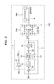
- FIG. 9 is a block diagram illustrating a digital filter according to a first embodiment.
- FIG. 10 is a block diagram illustrating an example of a minimum-value holder 51 of the digital filter illustrated in FIG. 9 .
- a digital filter 5 according to the first embodiment includes the minimum-value holder 51 , a drop detector 52 , a register 53 , and an output controller 54 .
- the minimum-value holder 51 receives an output code (measurement value) Vfo from the voltage-fluctuation observer 11 .
- the minimum-value holder 51 holds the minimum value of the measurement value Vfo received during M cycles (for example, 16 cycles (16 sampling points)), and outputs the held value as a held value Vhd.
- the voltage-fluctuation observer 11 receives the input voltage Vns, measures voltage fluctuations, and outputs the measurement value Vfo to the minimum-value holder 51 and the output controller 54 .
- the minimum-value holder 51 includes (M ⁇ 1) delay elements 511 and a minimum-value holder 512 , and outputs, to the minimum-value holder 512 , M pieces of data that are composed of the measurement value Vfo received from the voltage-fluctuation observer 11 and pieces of data delayed by one sampling cycle from one another by the delay elements 511 .
- the minimum-value holder 512 receives the M (for example, 16) pieces of sampling data and outputs the minimum value as the held value Vhd.
- a frequency (sampling frequency) Fck of the clock for acquiring the M pieces of sampling data from the measurement value Vfo in the minimum-value holder 51 is set at, for example, 5 GHz. Then, if the voltage-fluctuation frequency Fns is equal to or higher than one M-th of the sampling frequency Fck (Fns ⁇ Fck/M), the same minimum value is held throughout the total period, and is used as the held value Vhd.
- the drop detector 52 receives the minimum value (held value Vhd) held by the minimum-value holder 51 , and outputs an enable signal EN to the register 53 in a case where the held value Vhd remains minimum during predetermined N cycles (for example, 24 cycles).
- the register 53 receives the held value Vhd from the minimum-value holder 51 and stores the held value Vhd. In response to the enable signal EN from the drop detector 52 , the register 53 outputs, as the limit value Vlm, the held value Vhd remaining minimum during the N cycles, to the output controller 54 . Note that the drop detector 52 and the register 53 form a circuit that receives the held value Vhd and that outputs the held value Vhd as the limit value Vlm in the case where the held value Vhd remains minimum during the N cycles.
- the digital filter according to the first embodiment removes frequency components in a range equal to or higher than Fck/M, and thus does not remove frequency components lower than Fck/M.
- the same minimum value is held throughout the total period, and thus the held value Vhd (minimum value) is used as the limit value Vlm, without being changed.
- the amplitude of the voltage fluctuations of a frequency component (Fns ⁇ Fck/M) is automatically set as the limit value Vlm and is inputted to the output controller 54 .
- the output controller 54 receives the maximum value Vmx representing the upper limit, the measurement value Vfo, and the limit value Vlm. If the measurement value Vfo is smaller than the limit value Vlm, that is, if Vfo ⁇ Vlm holds true, the output controller 54 outputs the measurement value Vfo as the output value Vhc to the DCO 23 . If the measurement value Vfo is equal to or larger than the limit value Vlm, that is, if Vfo ⁇ Vlm holds true, the output controller 54 outputs the maximum value Vmx as the output value Vhc to the DCO 23 .
- the limit value Vlm is set at “0” for a frequency component lower than Fck/M. If a decrease in the minimum value (held value Vhd) of the measurement value Vfo is detected, the current value of the limit value Vlm is maintained. If the held value Vhd remains or increases during the N cycles, the limit value Vlm is updated to the current held value Vhd.
- FIG. 11 is a time chart for explaining an example of operation of the digital filter illustrated in FIG. 9 .
- Fns ⁇ Fck/M holds true for the voltage-fluctuation frequency Fns and that the measurement value Vfo has periodicity in cycles Tns.
- the same value is held as the held value Vhd (the minimum value of the measurement value Vfo) throughout the total period.
- M is the number of samples obtained by the minimum-value holder 51 , and is set at, for example, 16.
- Fck is a frequency of the sampling clock, and is set at, for example, 5 GHz.
- the register 53 controlled in accordance with the enable signal EN from the drop detector 52 outputs the held value Vhd (the minimum value of the measurement value Vfo) as the limit value Vlm to the output controller 54 . Since the measurement value Vfo ⁇ the limit value Vlm holds true throughout the total period, the output controller 54 outputs the maximum value Vmx as the output value Vhc to the DCO 23 .
- the power supply fluctuations voltage fluctuations (noise): Fns ⁇ Fck/M) in the frequency band equal to or higher than Fck/M are thereby cut off, and thus the clock frequency control is not performed.
- FIG. 12 is a time chart for illustrating another example of the operation of the digital filter illustrated in FIG. 9 .
- Fck/N ⁇ Fns ⁇ Fck/M holds true for the voltage-fluctuation frequency Fns
- a period in which the held value Vhd decreases is present in each of the N cycles (N ⁇ Tck). Accordingly, the limit value Vlm is not updated. In other words, it is determined that a drop in the measurement value Vfo occurs throughout the total period, and the limit value Vlm remains “0”.
- N is a predetermined number of cycles and is set at, for example, 24.
- the drop detector 52 determines whether the held value Vhd from the minimum-value holder 51 remains minimum during the period.
- the value of N may also be set at various values in a similar manner to the value of M described above. However, the embodiments are described under the assumption that M ⁇ N holds true.
- the output value Vhc outputted from the output controller 54 does not have a clock latency.
- the measurement value Vfo of the power supply fluctuations (Fck/N ⁇ Fns ⁇ Fck/M) in the frequency band that is equal to or higher than Fck/N and that is lower than Fck/M is thereby inputted as the output value Vhc without being changed, to the DCO 23 , and thus the clock frequency control is appropriately performed. In other words, a disadvantage of the clock frequency control performed on the particular-frequency-band voltage fluctuations may be avoided.
- FIG. 13 is a time chart for explaining a yet another example of the operation of the digital filter illustrated in FIG. 9 .
- Fck/4N ⁇ Fns ⁇ Fck/N holds true for the voltage-fluctuation frequency Fns, periods in which the held value Vhd does not decrease are present during the N cycles (N ⁇ Tck), and thus the limit value Vlm is updated.
- the measurement value Vfo falls below “0” (for example, periods represented by M ⁇ Tck in the measurement value Vfo in FIG. 13 ).
- the measurement value Vfo ⁇ the limit value Vlm does not hold true. Accordingly, in terms of the voltage-fluctuation frequency Fns, in both cases of the frequency band satisfying Fck/4N ⁇ Fns ⁇ Fck/N illustrated in FIG. 13 and the frequency band satisfying Fck/N ⁇ Fns ⁇ Fck/M described with reference to FIG. 12 , the same output value Vhc is outputted.
- the output value Vhc outputted from the output controller 54 does not have a clock latency.
- the measurement value Vfo of the power supply fluctuations (Fck/4N ⁇ Fns ⁇ Fck/N) in the frequency band that is higher than Fck/4N and that is lower than Fck/N is thereby inputted as the output value Vhc without being changed, to the DCO 23 , and thus the clock frequency control is appropriately performed.
- FIG. 14 is a time chart for explaining yet another example of the operation of the digital filter illustrated in FIG. 9 .
- Fns ⁇ Fck/4N holds true for the voltage-fluctuation frequency Fns
- the measurement value Vfo ⁇ the limit value Vlm holds true in periods in which the measurement value Vfo falls below “0”
- the maximum value Vmx is outputted as the output value Vhc.
- frequency components equal to or higher than Fck/M are removed, but desired output is not obtained from frequency components equal to or lower than Fck/4N. Accordingly, for example, a frequency band satisfying Fck/4N ⁇ Fns ⁇ Fck/M (N>M) is used.
- FIG. 15 is a graph illustrating a simulation result in the operation of the digital filter illustrated in FIG. 9 , and illustrates a case where a power supply is subjected to small-amplitude voltage fluctuations of a frequency component satisfying Fns ⁇ Fck/M and the first droop noise as being the large-amplitude frequency component satisfying Fck/4N ⁇ Fns ⁇ Fck/M.
- the digital filter according to the first embodiment removes the small-amplitude voltage fluctuations of the frequency component satisfying Fns ⁇ Fck/M and outputs only the large-amplitude voltage fluctuations of the frequency component satisfying Fck/4N ⁇ Fns ⁇ Fck/M.
- the digital filter according to the first embodiment enables the clock frequency control to be performed appropriately.
- a disadvantage of the clock frequency control may be avoided.
- FIGS. 16 to 18B are a diagram and graphs for explaining the clock frequency control performed in a case where the digital filter according to the first embodiment removes simultaneous switching noise, and for schematically explaining the advantageous effects described above with reference to FIGS. 11 to 15 .
- FIGS. 16 to 18B correspond to results of removing high frequency components in the clock frequency control described with reference to FIGS. 6 to 8B .
- FIG. 17A illustrates an input voltage Vns of the voltage-fluctuation observer 11 .
- FIG. 17B illustrates an output code from the voltage-fluctuation observer 11 (measurement value Vfo) and output (an output value) Vhc from the digital filter 5 .
- FIG. 17A the horizontal axis represents time (nsec), and the vertical axis represents voltage (V).
- FIG. 17B the horizontal axis represents time (nsec), and the vertical axis represents output code.
- FIG. 17A is the same as FIG. 7A described above, and the measurement value Vfo in FIG. 17B is the same as in FIG. 7B .
- FIG. 18A illustrates a case where the clock frequency control is performed without the digital filter 5 being provided, and is the same as FIG. 8B .
- FIG. 18B illustrates a case where the clock frequency control is performed with the digital filter 5 being provided.
- a timing-signal generation circuit 1 according to this embodiment or a semiconductor integrated circuit (semiconductor chip 100 ) according to this embodiment including the timing-signal generation circuit 1 includes the digital filter 5 that is provided between the voltage-fluctuation observer 11 and the adder 26 .
- the digital filter according to the first embodiment described with reference to FIGS. 9 to 15 may be applied to the digital filter 5 in FIG. 16 , and any one of the digital filters (described later) according to the second to eighth embodiments may also be applied to the digital filter 5 in FIG. 16 without any modification.
- the digital filter 5 is provided in a part subsequent to the voltage-fluctuation observer 11 to process the input voltage Vns illustrated in FIG. 17A .
- the measurement value Vfo is thereby converted into the output value Vhc as illustrated in FIG. 17B and then is inputted to the adder 26 .
- the clock frequency control performed on the first droop noise enables the setup slack to be improved and thus the timing constraint violation to be avoided.
- undesirable clock frequency control is not performed on the voltage fluctuations in a band equal to or higher than a predetermined frequency (for example, a frequency equal to or higher than Fck/M).
- a predetermined frequency for example, a frequency equal to or higher than Fck/M.
- FIG. 19 is a block diagram illustrating a digital filter according to the second embodiment.
- a digital filter 5 according to the second embodiment corresponds to a digital filter in which a moving-average filter 55 is added to the digital filter according to the first embodiment illustrated in FIG. 9 .
- the digital filter 5 includes the moving-average filter 55 that generates the maximum value Vmx, and thus has been improved to obtain desired output also for a frequency band satisfying Fns ⁇ Fck/4N.
- examples of the frequency band including a voltage-fluctuation frequency Fns satisfying Fck/4N include the second droop noise (for example, a frequency of approximately 1 MHz to approximately ten of MHz) described in FIG. 1 .
- the digital filter 5 also supports the voltage fluctuations in such a frequency band.
- the moving-average filter 55 inputs, for example, a moving average of the measurement value Vfo during L cycles as the maximum value Vmx, to the output controller 54 .
- the moving-average filter 55 functions as a low-pass filter, frequency components higher than Fck/L are attenuated, and frequency components equal to or lower than Fck/L pass through the moving-average filter 55 . Accordingly, the output value Vhc in the frequency band satisfying Fns ⁇ Fck/4N is also outputted.
- FIG. 20 is a time chart for explaining an example of operation of the digital filter illustrated in FIG. 19 .
- the second embodiment not “0” but a moving average value of the measurement value Vfo during L cycles is used as the maximum value Vmx in ranges in which the maximum value Vmx is outputted in a case where Fns ⁇ Fck/4N holds true, and thus the output value Vhc is the measurement value Vfo.
- FIG. 21 is a graph illustrating a simulation result in the operation of the digital filter illustrated in FIG. 19 .
- the power supply is subjected to small-amplitude voltage fluctuations (for example, the second droop noise) of a frequency component satisfying Fns ⁇ Fck/4N and the first droop noise as being the large-amplitude frequency component satisfying Fck/4N ⁇ Fns ⁇ Fck/M.
- small-amplitude voltage fluctuations for example, the second droop noise
- the digital filter according to the second embodiment removes the small-amplitude voltage fluctuations of the frequency component satisfying Fns ⁇ Fck/M, and thus outputs the large-amplitude voltage fluctuations of the frequency components satisfying Fck/4N ⁇ Fns ⁇ Fck/M and Fns ⁇ Fck/4N. This enables the clock frequency control to be performed appropriately also on the voltage fluctuations in the frequency band satisfying Fns ⁇ Fck/4N.
- FIG. 22 is a block diagram illustrating a digital filter according to the third embodiment.
- a digital filter 5 according to the third embodiment corresponds to a digital filter in which a minimum-measurement-value holder 56 is further added to the digital filter according to the first embodiment illustrated in FIG. 9 .
- a minimum-measurement-value holder 56 is provided in addition to the minimum-value holder 51 that holds the minimum value of the measurement value Vfo during M cycles (for example, 16 cycles) and outputs the minimum value as the held value Vhd.
- the minimum-measurement-value holder 56 is substantially the same holder as the minimum-value holder 51 , but holds the minimum value of the measurement value Vfo at K sampling points (in K cycles) in contrast with the M sampling points of the minimum-value holder 51 .
- the minimum-measurement-value holder 56 outputs the thus held minimum value as a minimum measurement value Vhd′.
- a value of K representing the K sampling points of the minimum-measurement-value holder 56 is set at, for example, M ⁇ K ⁇ 4M. For example, if M is set at 16, it is preferable to set K so as to satisfy 16 ⁇ K ⁇ 64.
- an output controller 54 ′ compares the limit value Vlm with the minimum measurement value Vhd′, instead of the measurement value Vfo.
- the output controller 54 ′ that compares the limit value Vlm with the minimum measurement value Vhd′ is also applied to the fourth embodiment in FIG. 25 , the seventh embodiment in FIG. 28 , and the eighth embodiment in FIG. 29 (described later).
- the output controllers 54 and 54 ′ may be considered to perform the same processing.
- the output controller 54 ′ If the minimum measurement value Vhd′ is smaller than the limit value Vlm, that is, if Vhd′ ⁇ Vlm holds true, the output controller 54 ′ outputs the measurement value Vfo as the output value Vhc to the DCO 23 . If the minimum measurement value Vhd′ is equal to or larger than the limit value Vlm, that is, Vhc′ ⁇ Vlm holds true, the output controller 54 ′ outputs the maximum value Vmx as the output value Vhc to the DCO 23 .
- FIG. 23 is a time chart for explaining an example of operation of the digital filter illustrated in FIG. 22 .
- the output value Vhc is outputted in the case of Fck/N ⁇ Fns ⁇ Fck/M, in such a manner that the minimum measurement value Vhd′ curves like an envelope.
- the output value Vhc may have such a waveform that is shaped like an envelope including the minimum measurement value Vhd′ extended for a period of k ⁇ Tck in contrast with the measurement value Vfo.
- the envelope shape provides higher frequency control effects, for example, in a case where the clock frequency control is performed when Fck/M and 1/(8Td) become close to each other.
- FIG. 24 is a graph illustrating a simulation result in the operation of the digital filter illustrated in FIG. 22 .
- the power supply is subjected to the small-amplitude voltage fluctuations of the frequency component satisfying Fns ⁇ Fck/M and the large-amplitude first droop noise as being the frequency component satisfying Fck/4N ⁇ Fns ⁇ Fck/M.
- the digital filter according to the third embodiment generates such an output value Vhc that curves like the envelope of the minimum value of the measurement value Vfo, thus enabling the clock frequency control to be preferably performed when Fck/M and 1/(8Td) become close to each other.
- a value “8” of the output code corresponds to the value “0” of the output code in FIGS. 11 to 14, 20, and 23 .
- FIG. 25 is a block diagram illustrating a digital filter according to the fourth embodiment.
- a digital filter 5 according to the fourth embodiment corresponds to a digital filter obtained by combining the second embodiment and the third embodiment described above.
- the moving-average filter 55 and the minimum-measurement-value holder 56 are added to the digital filter according to the first embodiment illustrated in FIG. 9 .
- the output controller 54 ′ compares the minimum measurement value Vhd′ with the limit value Vlm in the same manner as in the third embodiment. If Vhd′ ⁇ Vlm holds true, the output controller 54 ′ outputs the measurement value Vfo as the output value Vhc to the DCO 23 . If Vhd′ ⁇ Vlm holds true, the output controller 54 ′ outputs the maximum value Vmx as the output value Vhc to the DCO 23 .
- the digital filter according to the fourth embodiment exerts the advantageous effects exerted in both the second embodiment and the third embodiment.
- FIG. 26 is a block diagram illustrating a digital filter according to the fifth embodiment.
- a digital filter 5 according to the fifth embodiment corresponds to a digital filter in which J pieces of delay elements 57 - 1 to 57 -J and a 1-adder 58 that adds only “1” to a processing target are added to the digital filter according to the first embodiment.
- the digital filter 5 is designed to obtain a maximum value Vmx resulting from addition of “1” to an output value Vhc that is 3 cycles earlier. Specifically, when a relation between the measurement value Vfo and the limit value Vlm changes from Vfo ⁇ Vlm to Vfo ⁇ Vlm, the output value Vhc changes from the measurement value Vfo to the maximum value Vmx in just one cycle.
- the output value Vhc changes at once in one cycle.
- an increment of the output value Vhc is restricted in such a manner that an output value from the delay elements 57 - 1 to 57 -J that is J cycles earlier is incremented by only “1” by the 1-adder 58 .
- FIG. 27 is a block diagram illustrating a digital filter according to the sixth embodiment, and corresponds to a combination of the second embodiment described with reference to FIG. 19 and the fifth embodiment described with reference to FIG. 26 .
- a minimum-value selecting and holding device 59 receives output from the moving-average filter (a first-maximum-value generator) 55 in FIG. 19 as a first maximum value Vmx 1 as well as output from the 1-adder (a second-maximum-value generator) 58 in FIG. 26 as a second maximum value Vmx 2 .
- the delay elements 57 - 1 to 57 -J and the 1-adder 58 form the second-maximum-value generator.
- the minimum-value selecting and holding device 59 selects a smaller one of the first maximum value Vmx 1 and the second maximum value Vmx 2 as a maximum value Vmx, and outputs the selected one to the output controller 54 .
- the digital filter according to the sixth embodiment enables enhancement of the advantageous effects of the clock frequency control in addition to the advantageous effects in the second embodiment described above.
- FIG. 28 is a block diagram illustrating a digital filter according to the seventh embodiment, and corresponds to a combination of the third embodiment described with reference to FIG. 22 and the fifth embodiment described with reference to FIG. 26 .
- the digital filter according to the seventh embodiment enables enhancement of the advantageous effects of the clock frequency control in addition to the advantageous effects in the third embodiment described above.
- FIG. 29 is a block diagram illustrating a digital filter according to the eighth embodiment, and corresponds to a combination of the sixth embodiment described with reference to FIG. 27 and the third embodiment described with reference to FIG. 22 , that is, a combination of the second, third, and fifth embodiments.
- the digital filter according to the eighth embodiment enables enhancement of the advantageous effects of the clock frequency control in addition to the advantageous effects in the second and third embodiments described above.
- FIGS. 30 to 32B are a diagram and graphs for explaining the clock frequency control performed in a case where the digital filter according to the eighth embodiment removes simultaneous switching noise.
- FIG. 30 corresponds to FIG. 16 described above
- FIG. 31A corresponds to FIG. 17A described above
- FIG. 32A corresponds to FIG. 18A described above.
- a digital filter 5 according to the eighth embodiment is provided between the voltage-fluctuation observer 11 and the adder 26 , and is designed to process a measurement value Vfo from the voltage-fluctuation observer 11 and to output an output value Vhc to the adder 26 .
- Vfo the measurement value from the voltage-fluctuation observer 11
- Vhc the output value
- the digital filter according to the eighth embodiment enables removal of high frequency components further than in the first embodiment and enables obtaining an output value Vhc that is made not to change sharply.
- the eighth embodiment enables output, based on the measurement value Vfo, of the output value Vhc leading to easier voltage fluctuation compensation in the clock frequency control than in the first embodiment.
- the digital filter according to the eighth embodiment further enhances the advantageous effects of the clock frequency control in addition to the advantageous effects in the first embodiment.
- the setup-slack worst-value parts indicated by the arrows in FIG. 32B have been improved.
- M cycles for the minimum-value holder 51 may have various set values.
- the N cycles for the drop detector 52 may have various set values.
- the K cycles for the minimum-measurement-value holder 56 may have various set values.
- the L cycles for the moving-average filter 55 may have various set values.
- the frequency band of the voltage fluctuations to be reduced by the digital filters according to the embodiments is not limited to the first droop noise based on the resonance frequency of the semiconductor integrated circuit package.
- the voltage-fluctuation frequency band in which the disadvantage of the clock frequency control is avoidable is not limited to tens of MHz to hundreds of MHz corresponding to the first droop noise.
Landscapes
- Engineering & Computer Science (AREA)
- Physics & Mathematics (AREA)
- Electromagnetism (AREA)
- General Physics & Mathematics (AREA)
- Radar, Positioning & Navigation (AREA)
- Automation & Control Theory (AREA)
- Stabilization Of Oscillater, Synchronisation, Frequency Synthesizers (AREA)
- Logic Circuits (AREA)
Abstract
Description
- [Document 1] Japanese Laid-open Patent Publication No. 2008-099163,
- [Document 2] Japanese Laid-open Patent Publication No. 2005-102197,
- [Document 3] U.S. Pat. No. 8,222,936, Specification; and
- [Document 4] Charles R. Lefurgy et al., “Active Management of Timing Guardband to Save Energy in POWER7 (registered trademark)”, MICRO 44, pp. 1-11, Dec. 3-7, 2011.
Claims (14)
Applications Claiming Priority (2)
| Application Number | Priority Date | Filing Date | Title |
|---|---|---|---|
| JP2014-057034 | 2014-03-19 | ||
| JP2014057034A JP2015179998A (en) | 2014-03-19 | 2014-03-19 | Digital filter, timing signal generation circuit, and semiconductor integrated circuit |
Publications (2)
| Publication Number | Publication Date |
|---|---|
| US20150268679A1 US20150268679A1 (en) | 2015-09-24 |
| US9658630B2 true US9658630B2 (en) | 2017-05-23 |
Family
ID=54142049
Family Applications (1)
| Application Number | Title | Priority Date | Filing Date |
|---|---|---|---|
| US14/634,354 Expired - Fee Related US9658630B2 (en) | 2014-03-19 | 2015-02-27 | Digital filter and timing signal generation circuit |
Country Status (2)
| Country | Link |
|---|---|
| US (1) | US9658630B2 (en) |
| JP (1) | JP2015179998A (en) |
Citations (7)
| Publication number | Priority date | Publication date | Assignee | Title |
|---|---|---|---|---|
| US20010024454A1 (en) * | 2000-03-16 | 2001-09-27 | Fujitsu Limited | Resynchronous control apparatus of subscriber communication machine, and resynchronizing method |
| US20050047040A1 (en) | 2003-09-03 | 2005-03-03 | Naffziger Samuel D. | System and method to mitigate voltage fluctuations |
| JP2008099163A (en) | 2006-10-16 | 2008-04-24 | Audio Technica Corp | Noise canceling headphones and noise canceling method for headphones |
| US20100061722A1 (en) * | 2008-09-08 | 2010-03-11 | Fujitsu Limited | Network design apparatus and network design method |
| US7747972B2 (en) * | 2006-12-07 | 2010-06-29 | Infineon Technologies Ag | Methods and apparatuses for timing analysis of electronic circuits |
| US8222936B2 (en) | 2009-09-13 | 2012-07-17 | International Business Machines Corporation | Phase and frequency detector with output proportional to frequency difference |
| US20130100811A1 (en) * | 2010-06-14 | 2013-04-25 | Ntt Electronics Corporation | Output Rate Controller and Output Rate Control Method |
Family Cites Families (6)
| Publication number | Priority date | Publication date | Assignee | Title |
|---|---|---|---|---|
| JPH0856151A (en) * | 1994-08-12 | 1996-02-27 | Nec Miyagi Ltd | Voltage controlled ocsillation circuit |
| JP3360667B2 (en) * | 1999-12-01 | 2002-12-24 | 日本電気株式会社 | Synchronization method of phase locked loop, phase locked loop, and semiconductor device provided with the phase locked loop |
| JP3993818B2 (en) * | 2002-12-16 | 2007-10-17 | 松下電器産業株式会社 | Playback signal processing device |
| JP5470574B2 (en) * | 2008-06-16 | 2014-04-16 | 株式会社コルグ | Peak level detector |
| JP2013077869A (en) * | 2011-09-29 | 2013-04-25 | Japan Radio Co Ltd | Time-digital converter and pll circuit |
| JP2013090132A (en) * | 2011-10-18 | 2013-05-13 | Renesas Mobile Corp | Semiconductor device and radio communication terminal mounted with the same |
-
2014
- 2014-03-19 JP JP2014057034A patent/JP2015179998A/en active Pending
-
2015
- 2015-02-27 US US14/634,354 patent/US9658630B2/en not_active Expired - Fee Related
Patent Citations (8)
| Publication number | Priority date | Publication date | Assignee | Title |
|---|---|---|---|---|
| US20010024454A1 (en) * | 2000-03-16 | 2001-09-27 | Fujitsu Limited | Resynchronous control apparatus of subscriber communication machine, and resynchronizing method |
| US20050047040A1 (en) | 2003-09-03 | 2005-03-03 | Naffziger Samuel D. | System and method to mitigate voltage fluctuations |
| JP2005102197A (en) | 2003-09-03 | 2005-04-14 | Hewlett-Packard Development Co Lp | System and method for reducing voltage fluctuation |
| JP2008099163A (en) | 2006-10-16 | 2008-04-24 | Audio Technica Corp | Noise canceling headphones and noise canceling method for headphones |
| US7747972B2 (en) * | 2006-12-07 | 2010-06-29 | Infineon Technologies Ag | Methods and apparatuses for timing analysis of electronic circuits |
| US20100061722A1 (en) * | 2008-09-08 | 2010-03-11 | Fujitsu Limited | Network design apparatus and network design method |
| US8222936B2 (en) | 2009-09-13 | 2012-07-17 | International Business Machines Corporation | Phase and frequency detector with output proportional to frequency difference |
| US20130100811A1 (en) * | 2010-06-14 | 2013-04-25 | Ntt Electronics Corporation | Output Rate Controller and Output Rate Control Method |
Non-Patent Citations (1)
| Title |
|---|
| Lefurgy, Charles R., et al., "Active Management of Timing Guardband to Save Energy in POWER7", MICRO 44, pp. 1-11, Dec. 3-7, 2011. |
Also Published As
| Publication number | Publication date |
|---|---|
| US20150268679A1 (en) | 2015-09-24 |
| JP2015179998A (en) | 2015-10-08 |
Similar Documents
| Publication | Publication Date | Title |
|---|---|---|
| US10461755B2 (en) | Digitally assisted feedback loop for duty-cycle correction in an injection-locked PLL | |
| US10782763B2 (en) | Semiconductor device | |
| Grenat et al. | 5.6 adaptive clocking system for improved power efficiency in a 28nm x86-64 microprocessor | |
| US8390367B1 (en) | Ensuring minimum gate speed during startup of gate speed regulator | |
| US10382014B2 (en) | Adaptive oscillator for clock generation | |
| US9628089B1 (en) | Supply voltage tracking clock generator in adaptive clock distribution systems | |
| US8610473B2 (en) | Phase lock loop with adaptive loop bandwidth | |
| US9720380B2 (en) | Time-to-digital converter, frequency tracking apparatus and method | |
| US9312866B2 (en) | Phase lock loop (PLL/FLL) clock signal generation with frequency scaling to power supply voltage | |
| US10979048B2 (en) | Clock switching circuit and method | |
| JP2014052969A (en) | Clock frequency controller and semiconductor device | |
| US9658630B2 (en) | Digital filter and timing signal generation circuit | |
| US9553570B1 (en) | Crystal-less jitter attenuator | |
| JP5940413B2 (en) | Semiconductor device and electronic device | |
| CN102045042B (en) | Frequency signal generation method used in semiconductor device testing | |
| US12308844B2 (en) | Adaptive cyclic delay line for fractional-N PLL | |
| KR20120071786A (en) | Time to digital converter using successive approximation and the method thereof | |
| US9391624B1 (en) | Method and apparatus for avoiding dead zone effects in digital phase locked loops | |
| US10516390B2 (en) | Circuit to mitigate signal degradation in an isolation circuit | |
| KR20160076644A (en) | Spread spectrum clock generator based on sub-sampling phase locked loop and auto-calibration method using the same | |
| KR101697309B1 (en) | Delay lock loop circuit for wide band anti-harmonic lock and pdelay locking method thereof | |
| US12278643B2 (en) | Calibration for DTC fractional frequency synthesis | |
| US9083318B2 (en) | Digitally controlled oscillator and output frequency control method | |
| JP6318777B2 (en) | DESIGN METHOD, DESIGN DEVICE, AND PROGRAM | |
| Singh | Techniques for Improving Design Performance of VLSI Circuits and Systems |
Legal Events
| Date | Code | Title | Description |
|---|---|---|---|
| AS | Assignment |
Owner name: FUJITSU LIMITED, JAPAN Free format text: ASSIGNMENT OF ASSIGNORS INTEREST;ASSIGNOR:HASHIMOTO, TETSUTARO;REEL/FRAME:035079/0307 Effective date: 20150220 |
|
| STCF | Information on status: patent grant |
Free format text: PATENTED CASE |
|
| FEPP | Fee payment procedure |
Free format text: MAINTENANCE FEE REMINDER MAILED (ORIGINAL EVENT CODE: REM.); ENTITY STATUS OF PATENT OWNER: LARGE ENTITY |
|
| FEPP | Fee payment procedure |
Free format text: SURCHARGE FOR LATE PAYMENT, LARGE ENTITY (ORIGINAL EVENT CODE: M1554); ENTITY STATUS OF PATENT OWNER: LARGE ENTITY |
|
| MAFP | Maintenance fee payment |
Free format text: PAYMENT OF MAINTENANCE FEE, 4TH YEAR, LARGE ENTITY (ORIGINAL EVENT CODE: M1551); ENTITY STATUS OF PATENT OWNER: LARGE ENTITY Year of fee payment: 4 |
|
| FEPP | Fee payment procedure |
Free format text: MAINTENANCE FEE REMINDER MAILED (ORIGINAL EVENT CODE: REM.); ENTITY STATUS OF PATENT OWNER: LARGE ENTITY |
|
| LAPS | Lapse for failure to pay maintenance fees |
Free format text: PATENT EXPIRED FOR FAILURE TO PAY MAINTENANCE FEES (ORIGINAL EVENT CODE: EXP.); ENTITY STATUS OF PATENT OWNER: LARGE ENTITY |
|
| STCH | Information on status: patent discontinuation |
Free format text: PATENT EXPIRED DUE TO NONPAYMENT OF MAINTENANCE FEES UNDER 37 CFR 1.362 |
|
| FP | Lapsed due to failure to pay maintenance fee |
Effective date: 20250523 |