US9653138B1 - Magnetic memory and method of writing data - Google Patents
Magnetic memory and method of writing data Download PDFInfo
- Publication number
- US9653138B1 US9653138B1 US15/264,539 US201615264539A US9653138B1 US 9653138 B1 US9653138 B1 US 9653138B1 US 201615264539 A US201615264539 A US 201615264539A US 9653138 B1 US9653138 B1 US 9653138B1
- Authority
- US
- United States
- Prior art keywords
- potential
- magnetic layer
- write
- conductive line
- memory
- Prior art date
- Legal status (The legal status is an assumption and is not a legal conclusion. Google has not performed a legal analysis and makes no representation as to the accuracy of the status listed.)
- Active
Links
Images


Classifications
-
- G—PHYSICS
- G11—INFORMATION STORAGE
- G11C—STATIC STORES
- G11C11/00—Digital stores characterised by the use of particular electric or magnetic storage elements; Storage elements therefor
- G11C11/02—Digital stores characterised by the use of particular electric or magnetic storage elements; Storage elements therefor using magnetic elements
- G11C11/16—Digital stores characterised by the use of particular electric or magnetic storage elements; Storage elements therefor using magnetic elements using elements in which the storage effect is based on magnetic spin effect
- G11C11/165—Auxiliary circuits
- G11C11/1675—Writing or programming circuits or methods
-
- G—PHYSICS
- G11—INFORMATION STORAGE
- G11C—STATIC STORES
- G11C11/00—Digital stores characterised by the use of particular electric or magnetic storage elements; Storage elements therefor
- G11C11/02—Digital stores characterised by the use of particular electric or magnetic storage elements; Storage elements therefor using magnetic elements
- G11C11/16—Digital stores characterised by the use of particular electric or magnetic storage elements; Storage elements therefor using magnetic elements using elements in which the storage effect is based on magnetic spin effect
- G11C11/161—Digital stores characterised by the use of particular electric or magnetic storage elements; Storage elements therefor using magnetic elements using elements in which the storage effect is based on magnetic spin effect details concerning the memory cell structure, e.g. the layers of the ferromagnetic memory cell
-
- G—PHYSICS
- G11—INFORMATION STORAGE
- G11C—STATIC STORES
- G11C11/00—Digital stores characterised by the use of particular electric or magnetic storage elements; Storage elements therefor
- G11C11/02—Digital stores characterised by the use of particular electric or magnetic storage elements; Storage elements therefor using magnetic elements
- G11C11/16—Digital stores characterised by the use of particular electric or magnetic storage elements; Storage elements therefor using magnetic elements using elements in which the storage effect is based on magnetic spin effect
- G11C11/165—Auxiliary circuits
- G11C11/1673—Reading or sensing circuits or methods
-
- G—PHYSICS
- G11—INFORMATION STORAGE
- G11C—STATIC STORES
- G11C11/00—Digital stores characterised by the use of particular electric or magnetic storage elements; Storage elements therefor
- G11C11/02—Digital stores characterised by the use of particular electric or magnetic storage elements; Storage elements therefor using magnetic elements
- G11C11/16—Digital stores characterised by the use of particular electric or magnetic storage elements; Storage elements therefor using magnetic elements using elements in which the storage effect is based on magnetic spin effect
- G11C11/165—Auxiliary circuits
- G11C11/1677—Verifying circuits or methods
-
- G—PHYSICS
- G11—INFORMATION STORAGE
- G11C—STATIC STORES
- G11C2207/00—Indexing scheme relating to arrangements for writing information into, or reading information out from, a digital store
- G11C2207/002—Isolation gates, i.e. gates coupling bit lines to the sense amplifier
Definitions
- Embodiments described herein relate generally to a magnetic memory and a method of writing data.
- the basic structure of a memory cell of a magnetic memory for example, a magnetoresistive random-access memory (MRAM), consists of a storage layer (magnetic layer), a reference layer (magnetic layer), and a nonmagnetic layer between the storage and reference layers.
- the reference layer comprises a material or a structure in which the magnetization direction is difficult to reverse in comparison with the storage layer.
- the magnetization direction of the reference layer may be reversed at the time of a write operation because of manufacturing tolerances.
- FIG. 1 shows an example of a memory system.
- FIG. 2 shows an example of a magnetic memory.
- FIG. 3 shows the main part of the magnetic memory of FIG. 2 .
- FIG. 4 shows the relationships of the operation mode, input signals and the potential applied to bit lines.
- FIG. 5 shows an example of a potential selector.
- FIG. 6 shows an example of a memory cell.
- FIG. 7 to FIG. 13 show the hysteresis curves of magnetization reversal of a storage layer and a reference layer.
- FIG. 14 shows the first example of a write operation.
- FIG. 15 shows the relationship between an AP-write and an RL-initialization.
- FIG. 16 shows the second example of a write operation.
- FIG. 17 shows the relationship between an AP-write and an RL-initialization.
- FIG. 18 shows an example of a P-write.
- FIG. 19 shows the third example of a write operation.
- FIG. 20 shows the fourth example of a write operation.
- FIG. 21 shows the relationship between a write operation and a read operation.
- a magnetic memory comprises: a first magnetic layer; a second magnetic layer; a nonmagnetic layer between the first and second magnetic layers; a third magnetic layer synthetic-antiferromagnetic-coupled with the second magnetic layer; a first conductive line connected to the first magnetic layer;
- a controller controlling a read operation and a write operation, the write operation including a first operation, a second operation and a third operation, a first potential of the first conductive line being larger than a second potential of the second conductive line in the first operation, a third potential of the second conductive line being larger than a fourth potential of the first conductive line in the second operation, a fifth potential of the first conductive line being larger than a sixth potential of the second conductive line in the third operation, a first difference between the fifth and sixth potentials being smaller than a second difference between the first and second potentials, and the third operation being executed after the second operation and before the read operation.
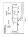
- FIG. 1 shows an example of a memory system.
- a memory system to which the present embodiment can be applied comprises a controller 10 and a magnetic memory (for example, an MRAM) 11 controlled by the controller 10 .
- the controller 10 is, for example, a host CPU or a memory controller.
- the controller 10 and the magnetic memory 11 may be separate chips, or may be included in a chip of a processor, etc.
- the controller 10 When data is written to the magnetic memory 11 , the controller 10 issues a write command and transfers it to the magnetic memory 11 .
- the controller 10 transfers a write address and write data to the magnetic memory 11 .
- the magnetic memory 11 transfers a reply of write completion to the controller 10 after accepting the write command.
- FIG. 2 shows an example of the magnetic memory.
- the magnetic memory 11 is, for example, an MRAM.
- the magnetic memory 11 comprises an interface portion 20 , a read/write controller 21 , a potential selector 22 , a word line driver/decoder 23 , a bit line driver/decoder 24 , a memory cell array 25 and a read circuit 26 .
- the interface portion 20 After accepting a write command, the interface portion 20 notifies the read/write controller 21 of the acceptance of the write command.
- the interface portion 20 transfers a write address to the word line driver/decoder 23 and the bit line driver/decoder 24 , and transfers write data to the bit line driver/decoder 24 .
- the read/write controller 21 controls a read operation and a write operation.
- a read operation is an operation of accessing the memory cell array 25 and outputting data read from the memory cell array 25 to the outside of the magnetic memory 11 .
- the read circuit 26 is activated.
- a read operation does not include a verify read operation (described later) for verifying whether or not a write operation has been performed correctly.
- a write operation is an operation of accessing the memory cell array 25 and writing write data to the memory cell array 25 .
- the read circuit 26 is activated temporarily. Data which is read from the memory cell array 25 in a verify read operation is not output to the outside of the magnetic memory 11 and is transferred to the read/write controller 21 (see the dotted arrow).
- the read/write controller 21 determines that a write operation has been completed, the read/write controller 21 notifies the interface portion 20 of the completion of the write operation.
- the interface portion 20 outputs a reply of write completion to the outside of the magnetic memory 11 .
- the potential selector 22 selects the potential to be applied to bit lines BL and bBL from a plurality of potentials based on, for example, a select signal from the read/write controller 21 .
- the selected potential is transferred to the bit line driver/decoder 24 .
- the word line driver/decoder 23 selects, for example, a word line WL from a plurality of word lines.
- the bit line driver/decoder selects, for example, a pair of bit lines BL and bBL from a plurality of pairs of bit lines.
- the word line driver/decoder 23 and the bit line driver/decoder 24 function as an access circuit which is allowed to access the memory cell array 25 in a read/write operation.
- FIG. 3 shows the main part of the magnetic memory of FIG. 2 .
- FIG. 4 shows the relationships of the operation mode, input signals Dw and bDw, and the potential Vread/write/initial applied to bit lines in the magnetic memory of FIG. 3 .
- the memory cell array 25 comprises a select transistor (for example, a field-effect transistor [FET]) T and a magnetoresistive element MTJ connected in series.
- the control terminal (gate) of the select transistor is connected to a word line WL.
- One of two current terminals of the select transistor T is connected to bit line BL.
- the magnetoresistive element MTJ is a two-terminal element. One end of the magnetoresistive element MTJ is connected to the other one of the two current terminals of the select transistor T. The other end of the magnetoresistive element MTJ is connected to bit line bBL.
- the bit line driver/decoder 24 comprises inverter circuit (driver) I 0 connected to bit line BL, and inverter circuit (driver) I 1 connected to bit line bBL.
- Inverter circuit I 0 comprises P-channel transistor (FET) P 0 and N-channel transistor (FET) N 0 connected in series between first and second supply terminals.
- Inverter circuit I 1 comprises P-channel transistor (FET) P 1 and N-channel transistor (FET) N 1 connected in series between first and second supply terminals.
- Inverter I 0 drives bit line BL based on input signal Dw.
- Inverter I 1 drives bit line bBL based on input signal bDw.
- Both of input signals Dw and bDw are binary signals (in other words, a signal having one of a low level and a high level).
- Input signal bDw is defined as the inversion signal of input signal Dw.
- the first supply terminals of inverter circuits I 0 and I 1 are set to Vread/write/initial.
- the second supply terminals of inverter circuits I 0 and I 1 are set to Vss.
- Vss is a ground potential.
- Vread/write/initial is a positive potential greater than Vss.
- Vread/write/initial is the potential selected by the potential selector 22 .
- the potential selector 22 comprises a multiplexer (MUX) 28 as shown in FIG. 5 .
- the multiplexer 28 selects one of four potentials Vap-p, Vp-ap, Vinitial and Vread based on a select signal SEL.
- Vap-p and Vp-ap are potentials used in a write operation.
- Vap-p is a potential used to change the state of the magnetoresistive element MTJ from an antiparallel state to a parallel state.
- Vp-ap is a potential used to change the state of the magnetoresistive element MTJ from a parallel state to an antiparallel state.
- the magnetoresistive element MTJ comprises a storage layer (magnetic layer), a reference layer (magnetic layer), and a nonmagnetic layer between the storage and reference layers.
- the reference layer comprises a material or a structure in which the magnetization direction is difficult to reverse in comparison with the storage layer.
- a parallel state indicates that the magnetization directions of the storage and reference layers are the same as each other.
- An antiparallel state indicates that the magnetization directions of the storage and reference layers are opposite to each other.
- a parallel state for example, the resistance of the magnetoresistive element MTJ is small. This state is called a 0-state, in which data 0 is stored.
- an antiparallel state for example, the resistance of the magnetoresistive element MTJ is large. This state is called a 1-state, in which data 1 is stored.
- the potential selector 22 selects Vap-p, and Vread/write/initial is set to Vap-p.
- Input signal Dw is set to 0 (low level).
- Input signal bDw is set to 1 (high level).
- Vap-p is applied to bit line BL.
- Vss is applied to bit line bBL.
- a write current from bit line BL to bit line bBL flows in the magnetoresistive element MTJ.
- the magnetoresistive element MTJ is transitioned from an antiparallel state to a parallel state.
- the potential selector 22 selects Vp-ap, and Vread/write/initial is set to Vp-ap.
- Input signal Dw is set to 1 (high level).
- Input signal bDw is set to 0 (low level).
- Vp-ap is applied to bit line bBL.
- Vss is applied to bit line BL.
- a write current from bit line bBL to bit line BL flows in the magnetoresistive element MTJ.
- the magnetoresistive element MTJ is transitioned from a parallel state to an antiparallel state.
- Vinitial is also a potential used in a write operation.
- Vinitial is a potential which is newly adopted in the present embodiment.
- Vinitial is an element unique to the present embodiment.
- the reference layer comprises a material or a structure in which the magnetization direction is difficult to reverse in comparison with the storage layer in the magnetoresistive element MTJ.
- the magnetization direction of the reference layer may be reversed at the time of a write operation because of manufacturing tolerances. If both of the magnetization directions of the storage and reference layers are reversed when the write data is 1 (AP-write), the magnetoresistive element MTJ is not transitioned to an antiparallel state after a write operation. Thus, correct data is not stored.
- Vinitial is a potential used to return the magnetization direction of the reference layer when the magnetization of the reference layer has been reversed unintentionally as mentioned above (the details will be described later).
- the read/write controller 21 When the magnetization of the reference layer has been reversed in a write operation (AP-write), the read/write controller 21 performs an initialization operation for returning the magnetization direction of the reference layer (RL-initialization) after the write operation and before a read operation. Whether or not the magnetization of the reference layer has been reversed can be verified by, for example, a verify read operation (shown by the dotted arrow in FIG. 3 ).
- an initialization operation may be performed in any case after the write operation and before a read operation regardless of whether or not the magnetization of the reference layer has been reversed. At this time, the value of write data may be confirmed in advance. If the write data is 1 (AP-write), an initialization operation may be performed.
- the potential selector 22 selects Vinitial based on a select signal SEL from the read/write controller 21 .
- Vread/write/initial is set to Vinitial.
- Input signal Dw is set to 0 (low level).
- Input signal bDw is set to 1 (high level).
- Vinitial is applied to bit line BL.
- Vss is applied to bit line bBL.
- an initialization current from bit line BL to bit line bBL flows in the magnetoresistive element MTJ.
- the magnetization direction of the reference layer is reversed.
- the value of Vinitial needs to be less than that of Vap-p.
- Vread is a potential used in a read operation.
- Vread is a potential used to read the state of the resistance of the magnetoresistive element MTJ (specifically, an antiparallel state or a parallel state), in other words, to read the data stored in the magnetoresistive element MTJ.
- Vread needs to be less than that of Vap-p and that of Vp-ap to prevent the magnetization reversal of the storage layer at the time of a read operation.
- the value of Vread may be different from or the same as that of Vinitial. If the value of Vread is different from that of Vinitial, for example, the value of Vread is less than that of Vinitial. This is because when the value of Vread is greater than that of Vinitial, Vinitial can be replaced by Vread (Vinitial can be omitted). Similarly, if the value of Vread is the same as that of Vinitial, Vinitial can be replaced by Vread, and thus, Vread may serve as Vinitial.
- the potential selector 22 selects Vread based on a select signal SEL from the read/write controller 21 .
- Vread/write/initial is set to Vread.
- Input signal Dw is set to 0 (low level).
- Input signal bDw is set to 1 (high level).
- Vread is applied to bit line BL.
- Vss is applied to bit line bBL.
- a read current from bit line BL to bit line bBL flows in the magnetoresistive element MTJ.
- the state of the resistance of the magnetoresistive element MTJ is read.
- the read circuit 26 is connected to a pair of bit lines BL and bBL via a switch circuit 27 .
- the read circuit 26 comprises, for example, two N-channel transistors (FET) N 2 and N 3 . In a read operation and a verify read operation, a read-enable signal RE is changed from a low level to a high level. Thus, the read circuit 26 is electrically connected to bit lines BL and bBL.
- FIG. 6 shows an example of a memory cell.
- the memory cell MC corresponds to the memory cell MC shown in FIG. 3 .
- the memory cell MC comprises a select transistor T and a magnetoresistive element MTJ connected in series between a pair of bit lines BL and bBL.
- the magnetoresistive element MTJ comprises a storage layer (magnetic layer) SL, a reference layer (magnetic layer) RL, and a nonmagnetic layer (tunnel barrier layer) TN between the storage and reference layers.
- the reference layer RL comprises a material or a structure in which the magnetization direction is difficult to reverse in comparison with the storage layer SL.
- the storage layer SL comprises a magnetic material such as CoFeB or FeB.
- the reference layer RL comprises a magnetic material such as CoPt, CoNi or CoPd.
- the nonmagnetic layer TN comprises an insulating layer formed of MgO, etc.
- the magnetoresistive element MTJ further comprises a magnetic layer SCL which is synthetic-antiferromagnetic-coupled (SAF-coupled) with the reference layer RL.
- a nonmagnetic layer for example, a metal layer
- ML may be provided as shown in this example, or may be omitted.
- SAF-coupling indicates a state in which the magnetic moment of two magnetic layers (the reference layer RL and the magnetic layer SCL) is the most stable when the magnetization directions of the two magnetic layers are antiparallel (opposite).
- the magnetic layer SCL may function as a shift-cancelling layer which cancels an effect of shift of the hysteresis curve of magnetization reversal of the storage layer SL due to the stray magnetic field from the reference layer RL.
- the magnetic layer SCL comprises a magnetic material such as CoPt, CoNi or CoPd.
- the storage layer SL, the reference layer RL and the magnetic layer SCL have a magnetization in a perpendicular direction in which they are stacked, in other words, a perpendicular magnetization.
- the storage layer SL, the reference layer RL and the magnetic layer SCL may have a magnetization in an in-plane direction perpendicular to the direction in which they are stacked, in other words, an in-plane magnetization.
- the hysteresis curves of magnetization reversal of the storage layer SL and the reference layer RL of the magnetoresistive element MTJ having the above structure are, for example, shown in FIG. 7 (normal mode).
- the horizontal axis indicates a write potential.
- the left side of 0 V shows the potential applied to the storage layer SL when the magnetic layer SCL is 0 V.
- the right side of 0 V shows the potential applied to the magnetic layer SCL when the storage layer SL is 0 V.
- the left vertical axis indicates the probability of downward magnetization, specifically, the probability that the magnetization direction of the storage layer SL or the reference layer RL turns downward.
- the right vertical axis indicates the probability of upward magnetization, specifically, the probability that the magnetization direction of the storage layer SL or the reference layer RL turns upward.
- the downward magnetization indicates that the magnetization direction of the storage layer SL or the reference layer RL is toward a side opposite to the magnetic layer SCL side in FIG. 6 .
- the upward magnetization indicates that the magnetization direction of the storage layer SL or the reference layer RL is toward the magnetic layer SCL side in FIG. 6 .
- the hysteresis curve of the magnetization direction of the storage layer SL is close to the 0 V line in comparison with the hysteresis curve of magnetization reversal of the reference layer RL.
- the potential in which the magnetization of the storage layer SL is reversed is less than that in which the magnetization of the reference layer RL is reversed.
- each of the potential in which the magnetization of the storage layer SL is reversed and the potential in which the magnetization of the reference layer RL is reversed exhibits a distribution because of manufacturing tolerances, etc.
- the Vp-ap line may intersect with the hysteresis curve of magnetization reversal of the reference layer RL (specifically, the portion of change from 0 to 100% in the right axis).
- the magnetization direction of the reference layer RL is reversed based on a constant probability P (0% ⁇ P ⁇ 100%).
- both of the magnetization directions of the storage and reference layers SL and RL of the magnetoresistive element MTJ may be upward after an AP-write.
- This state is equivalent to a parallel state.
- the state of the resistance of the magnetoresistive element MTJ is a parallel state (0-state) although an AP-write (1-writing) has been performed.
- a normal magnetoresistive element MTJ In a normal magnetoresistive element MTJ, if the above failure mode has been generated, the magnetoresistive element MTJ becomes a hardware defective element. The element cannot be recovered. In a normal magnetoresistive element MTJ, as shown in FIG. 9 (failure mode), the hysteresis curve of the magnetization direction of the storage layer SL is always close to the 0 V line in comparison with the hysteresis curve of magnetization reversal of the reference layer RL.
- a normal magnetoresistive element MTJ indicates a case where SAF-coupling between the reference layer RL and the magnetic layer SCL is not present, or a case where the magnetic layer SCL and the nonmagnetic layer ML are omitted, in the magnetoresistive element MTJ shown in FIG. 6 .
- curve X (a case of failure) indicating the probability that the magnetization direction of the reference layer RL turns downward (in the left vertical axis) is shifted to a position close to the 0 V line in comparison with a case of normal.
- curve X indicating the probability that the magnetization direction of the reference layer RL turns downward (in the left vertical axis) is close to the 0 V line in comparison with curve Y indicating the probability that the magnetization direction of the storage layer SL turns downward (in the left vertical axis).
- the magnetization direction of the reference layer RL is returned spontaneously by an effect of the above SAF-coupling when the voltage applied to the magnetoresistive element MTJ is set to zero after a write operation.
- the effect of SAF-coupling varies because of manufacturing tolerances, etc.
- a magnetoresistive element MTJ in which the magnetization directions of the reference layer RL and the magnetic layer SCL are the same remains based on a constant probability even when the voltage applied to the magnetoresistive element MTJ is set to zero after a write operation.
- Vinitial is set between two curves X and Y. Further, an initialization operation (RL-initialization) for applying Vinitial to the magnetoresistive element MTJ is performed after a write operation (AP-write). In this manner, only the magnetization direction of the reference layer RL can be reversed. The magnetization direction of the reference layer RL can be initialized (turned downward). It should be noted that Vinitial is not set to zero and is set to a value which allows the magnetization direction of the reference layer RL to 100% turn downward.
- the magnetoresistive element MTJ does not become a hardware defective element.
- the magnetoresistive element MTJ can be recovered by the initialization operation (RL-initialization) shown in FIG. 10 .
- the magnetization directions of all of the storage layer SL, the reference layer RL and the magnetic layer SCL have turned upward by an AP-write, only the magnetization direction of the reference layer RL can be changed to a downward direction by applying an initialization operation (RL-initialization) using Vinitial. In this way, the state of the magnetoresistive element MTJ can be returned to a normal antiparallel state.
- Vinitial is set to the P-write side (left side) of the 0 V line.
- the polarity of the voltage which is applied to the magnetoresistive element MTJ in a P-write and an RL-initialization is opposite to that of the voltage which is applied to the magnetoresistive element MTJ in an AP-write.
- Vread can be selected from the following patterns.
- Vread can be set to the P-write side (left side) of the 0 V line in a manner similar to that of Vinitial.
- the polarity of the voltage applied to the magnetoresistive element MTJ is the same in a P-write, an RL-initialization and a read operation. It should be noted that Vread is less than Vap-p and Vinitial.
- Vread may be located on the P-write side (left side) of the 0 V line and equal to Vinitial.
- the polarity of the voltage applied to the magnetoresistive element MTJ is the same in a P-write, an RL-initialization and a read operation. In this case, Vread is used in place of Vinitial.
- Vread may be set to the AP-write side (right side) of the 0 V line.
- the polarity of the voltage which is applied to the magnetoresistive element MTJ in a P-write and an RL-initialization is different from that of the voltage which is applied to the magnetoresistive element MTJ in an AP-write and a read operation. Note that Vread is less than Vp-ap.
- the above patterns are examples in which a failure mode occurs in an AP-write. This is because the margin between the potential in which the magnetization direction of the storage layer SL turns upward and the potential in which the magnetization direction of the reference layer RL turns upward is generally small in terms of the design of the magnetic memory. Note that, even when a failure mode has occurred in a P-write, recovery may be performed based on the same principle of the recovery from a failure mode in an AP-write.
- FIG. 14 shows the first example of a write operation.
- the first example is a flowchart in which the initialization operation of the reference layer is performed after a write operation and before a read operation regardless of the value of write data.
- a write operation is performed (steps ST 11 and ST 12 ).
- the initialization operation of the reference layer (RL-initialization) is performed (step ST 13 ). After the initialization operation of the reference layer, it is determined that the write operation has been performed correctly.
- the initialization operation of the reference layer is performed using Vinitial.
- Vread is equal to Vinitial
- the initialization operation of the reference layer using Vinitial may be replaced by the initialization operation (dummy read operation) of the reference layer using Vread.
- FIG. 15 shows the relationship between the potential of the selected word line WL and the potential of the selected pair of bit lines BL and bBL in the first example of a write operation.
- the selected word line WL and the selected pair of bit lines BL and bBL refer to the word line and the pair of bit lines connected to the memory cell to which write data is written.
- a write operation and an initialization operation are performed continuously.
- a write operation and an initialization operation are preferably performed without changing the potential of the selected word line WL, in other words, while maintaining the state (high level) in which the word line WL is selected. In this manner, it is possible to eliminate the swing of the word line WL and contribute to the reduction in consumed power of the memory system.
- Vp-ap When the write operation is an AP-write, Vp-ap is applied to bit line BL, and Vss is applied to bit line bBL.
- Vp-ap When the write operation is an AP-write, Vp-ap is applied to bit line BL, and Vss is applied to bit line bBL.
- the magnetoresistive element MTJ In a normal write operation (normal), the magnetoresistive element MTJ is transitioned from a parallel state to an antiparallel state. However, in a write operation in which the magnetization direction of the reference layer is reversed (failure), the magnetoresistive element MTJ maintains its parallel state substantially.
- the initialization operation of the reference layer is performed.
- Vinitial (Vread in a dummy read operation) is applied to bit line bBL, and Vss is applied to bit line BL.
- Vss is applied to bit line BL.
- FIG. 16 shows the second example of a write operation.
- the second example is a flowchart in which a verify read operation is performed after a write operation to verify whether or not the magnetization of the reference layer has been reversed, and further, the initialization operation of the reference layer is performed after the write operation and before a read operation when the magnetization reversal of the reference layer has been confirmed.
- a verify read operation is performed. With this operation, it is possible to appropriately perform the initialization operation of the reference layer of a memory cell in which the magnetization of the reference layer has been reversed.
- a write operation is performed (steps ST 21 and ST 22 ).
- a verify read operation is performed to verify whether or not the magnetization of the reference layer has been reversed (step ST 23 ).
- the read potential Vread used for the verify read operation is less than Vinitial, or has a polarity different from that of Vinitial.
- write data is compared with read data (step ST 24 ). If they are matched, it is determined that the write operation has been performed correctly.
- the initialization operation of the reference layer (RL-initialization) is performed (step ST 25 ). After the initialization operation of the reference layer, it is determined that the write operation has been performed correctly.
- FIG. 17 shows the relationship between the potential of the selected word line WL and the potential of the selected pair of bit lines BL and bBL in the second example of a write operation.
- a write operation, a verify read operation and an initialization operation are performed continuously.
- a write operation, a verify read operation and an initialization operation are preferably performed without changing the potential of the selected word line WL, in other words, while maintaining the state (high level) in which the word line WL is selected.
- Vp-ap When the write operation is an AP-write, Vp-ap is applied to bit line BL, and Vss is applied to bit line bBL.
- Vp-ap When the write operation is an AP-write, Vp-ap is applied to bit line BL, and Vss is applied to bit line bBL.
- the magnetoresistive element MTJ In a normal write operation (normal), the magnetoresistive element MTJ is transitioned from a parallel state to an antiparallel state. However, in a write operation in which the magnetization direction of the reference layer is reversed (failure), the magnetoresistive element MTJ maintains its parallel state substantially.
- a verify read operation is performed subsequent to the write operation.
- Vread is applied to bit line bBL
- Vss is applied to bit line BL.
- the read data from the memory cell is compared with write data. If they are mismatched, it is determined that the magnetization direction of the reference layer has been reversed.
- the initialization operation of the reference layer is performed.
- Vinitial is applied to bit line bBL
- Vss is applied to bit line BL.
- the magnetization direction of the reference layer of the magnetoresistive element MTJ is returned.
- the magnetoresistive element MTJ is transitioned from a parallel state to an antiparallel state correctly.
- the initialization operation of the reference layer may not be performed in any case.
- the possibility that the magnetization direction of the reference layer is reversed is small in comparison with an AP-write.
- FIG. 19 shows the third example of a write operation.
- the value of write data is checked in advance before a write operation.
- the processing of the subsequent write operation is changed based on the value of write data.
- the value of write data is checked (steps ST 31 and ST 32 ). If the write data is 0, a P-write is performed (step ST 33 _ 0 ). In this case, the write operation is terminated without performing the initialization operation of the reference layer. If the write data is 1, an AP-write is performed (step ST 33 _ 1 ). In this case, the initialization operation of the reference layer (RL-initialization) is performed after the write operation (step ST 34 ). After the initialization operation of the reference layer, it is determined that the write operation has been performed correctly.
- the initialization operation of the reference layer in a P-write, can be omitted.
- the write speed of P-write can be improved.
- correct data can be stored by the initialization operation of the reference layer.
- FIG. 20 shows the fourth example of a write operation.
- the fourth example is a combination of the second and third examples.
- the value of write data is checked in advance before a write operation. If the write data is 1 (AP-write), a verify read operation is performed after the write operation to verify whether or not the magnetization of the reference layer has been reversed. When the magnetization reversal of the reference layer has been confirmed, the initialization operation of the reference layer is performed.
- step ST 41 and ST 42 After accepting a write command, the value of write data is checked (steps ST 41 and ST 42 ). If the write data is 0, a P-write is performed (step ST 43 _ 0 ). In this case, the write operation is terminated without performing the initialization operation of the reference layer.
- step ST 43 _ 1 If the write data is 1, an AP-write is performed (step ST 43 _ 1 ). In this case, after the AP-write, a verify read operation is performed to verify whether or not the magnetization of the reference layer has been reversed (step ST 44 ). Subsequently, write data is compared with read data (step ST 45 ).
- the write operation is terminated without performing the initialization operation of the reference layer.
- the initialization operation of the reference layer is performed (step ST 46 ). After the initialization operation of the reference layer, it is determined that the write operation has been performed correctly.
- the write speed of P-write can be improved since the initialization operation of the reference layer can be omitted in a P-write.
- a verify read operation is performed to verify whether or not the magnetization of the reference layer has been reversed. When the magnetization reversal of the reference layer has been confirmed, the initialization operation of the reference layer is performed. Thus, correct data can be stored.
- FIG. 21 shows the relationship between a write operation and a read operation.
- This example shows a case where a read operation is performed after an AP-write, and a case where a read operation is performed after a P-write.
- a verify read operation and the initialization operation of the reference layer are performed after an AP-write and before a read operation.
- write data 1 is written to the memory cell correctly.
- the magnetoresistive element of the memory cell is transitioned to an AP-state correctly.
- correct data can be read from the memory cell in a read operation after the AP-write.
- Write data 0 is written to the memory cell correctly by a P-write.
- the magnetoresistive element of the memory cell is transitioned to a P-state correctly by the P-write.
- correct data can be read from the memory cell in a read operation after the P-write.
Abstract
Description
Claims (20)
Priority Applications (1)
| Application Number | Priority Date | Filing Date | Title |
|---|---|---|---|
| US15/264,539 US9653138B1 (en) | 2016-03-02 | 2016-09-13 | Magnetic memory and method of writing data |
Applications Claiming Priority (2)
| Application Number | Priority Date | Filing Date | Title |
|---|---|---|---|
| US201662302461P | 2016-03-02 | 2016-03-02 | |
| US15/264,539 US9653138B1 (en) | 2016-03-02 | 2016-09-13 | Magnetic memory and method of writing data |
Publications (1)
| Publication Number | Publication Date |
|---|---|
| US9653138B1 true US9653138B1 (en) | 2017-05-16 |
Family
ID=58670579
Family Applications (1)
| Application Number | Title | Priority Date | Filing Date |
|---|---|---|---|
| US15/264,539 Active US9653138B1 (en) | 2016-03-02 | 2016-09-13 | Magnetic memory and method of writing data |
Country Status (1)
| Country | Link |
|---|---|
| US (1) | US9653138B1 (en) |
Cited By (1)
| Publication number | Priority date | Publication date | Assignee | Title |
|---|---|---|---|---|
| US20230095205A1 (en) * | 2021-09-29 | 2023-03-30 | Hewlett Packard Enterprise Development Lp | Selection of a transmitting vap for a mbssid set |
Citations (7)
| Publication number | Priority date | Publication date | Assignee | Title |
|---|---|---|---|---|
| US7414881B2 (en) * | 2004-03-31 | 2008-08-19 | Nec Corporation | Magnetization direction control method and application thereof to MRAM |
| WO2010100678A1 (en) | 2009-03-06 | 2010-09-10 | 株式会社日立製作所 | Tunnel magnetic recording element, magnetic memory cell, and magnetic random access memory |
| US8374048B2 (en) | 2010-08-11 | 2013-02-12 | Grandis, Inc. | Method and system for providing magnetic tunneling junction elements having a biaxial anisotropy |
| US8520433B1 (en) * | 2012-03-21 | 2013-08-27 | Kabushiki Kaisha Toshiba | Magnetoresistive element and magnetic memory |
| US8680633B1 (en) * | 2012-09-21 | 2014-03-25 | Kabushiki Kaisha Toshiba | Magnetoresistive element and magnetic memory |
| US8836061B2 (en) * | 2012-06-06 | 2014-09-16 | Avalanche Technology, Inc. | Magnetic tunnel junction with non-metallic layer adjacent to free layer |
| US20140284741A1 (en) | 2011-11-30 | 2014-09-25 | Sony Corporation | Storage element and storage apparatus |
-
2016
- 2016-09-13 US US15/264,539 patent/US9653138B1/en active Active
Patent Citations (7)
| Publication number | Priority date | Publication date | Assignee | Title |
|---|---|---|---|---|
| US7414881B2 (en) * | 2004-03-31 | 2008-08-19 | Nec Corporation | Magnetization direction control method and application thereof to MRAM |
| WO2010100678A1 (en) | 2009-03-06 | 2010-09-10 | 株式会社日立製作所 | Tunnel magnetic recording element, magnetic memory cell, and magnetic random access memory |
| US8374048B2 (en) | 2010-08-11 | 2013-02-12 | Grandis, Inc. | Method and system for providing magnetic tunneling junction elements having a biaxial anisotropy |
| US20140284741A1 (en) | 2011-11-30 | 2014-09-25 | Sony Corporation | Storage element and storage apparatus |
| US8520433B1 (en) * | 2012-03-21 | 2013-08-27 | Kabushiki Kaisha Toshiba | Magnetoresistive element and magnetic memory |
| US8836061B2 (en) * | 2012-06-06 | 2014-09-16 | Avalanche Technology, Inc. | Magnetic tunnel junction with non-metallic layer adjacent to free layer |
| US8680633B1 (en) * | 2012-09-21 | 2014-03-25 | Kabushiki Kaisha Toshiba | Magnetoresistive element and magnetic memory |
Cited By (1)
| Publication number | Priority date | Publication date | Assignee | Title |
|---|---|---|---|---|
| US20230095205A1 (en) * | 2021-09-29 | 2023-03-30 | Hewlett Packard Enterprise Development Lp | Selection of a transmitting vap for a mbssid set |
Similar Documents
| Publication | Publication Date | Title |
|---|---|---|
| US9536621B2 (en) | Nonvolatile memory | |
| US10446204B2 (en) | Semiconductor memory device | |
| KR102131812B1 (en) | Source line floating circuit, memory device and method of reading data using the same | |
| US10410707B2 (en) | Nonvolatile memory | |
| US10431303B2 (en) | Resistance change type memory including write control circuit to control write to variable resistance element | |
| US9728239B2 (en) | Semiconductor memory device | |
| JP2011138598A (en) | Nonvolatile memory | |
| US9824736B1 (en) | Memory device | |
| US10593375B2 (en) | Semiconductor memory device with correcting resistances in series with memory array signal lines | |
| US9595311B2 (en) | Nonvolatile semiconductor memory device | |
| CN109196587B (en) | Semiconductor circuit, driving method, and electronic apparatus | |
| US10446211B2 (en) | Semiconductor storage device | |
| US10410706B2 (en) | Resistance change type memory | |
| US9966123B2 (en) | Semiconductor memory device with write driver | |
| US9773538B2 (en) | Nonvolatile semiconductor memory | |
| US8498144B2 (en) | Semiconductor storage device | |
| US10446739B2 (en) | Semiconductor memory device | |
| US9653138B1 (en) | Magnetic memory and method of writing data | |
| TWI790497B (en) | semiconductor memory device | |
| US10311931B2 (en) | Semiconductor memory device | |
| US20170076791A1 (en) | Semiconductor memory device | |
| US9672887B2 (en) | Semiconductor memory capable of reading data without accessing memory cell | |
| US10403346B2 (en) | Semiconductor memory device | |
| Yahya et al. | Designing low-V Th STT-RAM for write energy reduction in scaled technologies | |
| CN112927737A (en) | Non-volatile register with magnetic tunnel junction |
Legal Events
| Date | Code | Title | Description |
|---|---|---|---|
| AS | Assignment |
Owner name: KABUSHIKI KAISHA TOSHIBA, JAPAN Free format text: ASSIGNMENT OF ASSIGNORS INTEREST;ASSIGNORS:HASHIMOTO, YUTAKA;NISHIYAMA, KATSUYA;SIGNING DATES FROM 20160927 TO 20161006;REEL/FRAME:041025/0321 |
|
| STCF | Information on status: patent grant |
Free format text: PATENTED CASE |
|
| AS | Assignment |
Owner name: TOSHIBA MEMORY CORPORATION, JAPAN Free format text: ASSIGNMENT OF ASSIGNORS INTEREST;ASSIGNOR:KABUSHIKI KAISHA TOSHIBA;REEL/FRAME:043709/0035 Effective date: 20170706 |
|
| MAFP | Maintenance fee payment |
Free format text: PAYMENT OF MAINTENANCE FEE, 4TH YEAR, LARGE ENTITY (ORIGINAL EVENT CODE: M1551); ENTITY STATUS OF PATENT OWNER: LARGE ENTITY Year of fee payment: 4 |
|
| AS | Assignment |
Owner name: K.K. PANGEA, JAPAN Free format text: MERGER;ASSIGNOR:TOSHIBA MEMORY CORPORATION;REEL/FRAME:055659/0471 Effective date: 20180801 Owner name: TOSHIBA MEMORY CORPORATION, JAPAN Free format text: CHANGE OF NAME AND ADDRESS;ASSIGNOR:K.K. PANGEA;REEL/FRAME:055669/0401 Effective date: 20180801 Owner name: KIOXIA CORPORATION, JAPAN Free format text: CHANGE OF NAME AND ADDRESS;ASSIGNOR:TOSHIBA MEMORY CORPORATION;REEL/FRAME:055669/0001 Effective date: 20191001 |