US9646545B2 - Display device - Google Patents
Display device Download PDFInfo
- Publication number
- US9646545B2 US9646545B2 US15/239,403 US201615239403A US9646545B2 US 9646545 B2 US9646545 B2 US 9646545B2 US 201615239403 A US201615239403 A US 201615239403A US 9646545 B2 US9646545 B2 US 9646545B2
- Authority
- US
- United States
- Prior art keywords
- circuit board
- display panel
- back cabinet
- cabinet
- liquid crystal
- Prior art date
- Legal status (The legal status is an assumption and is not a legal conclusion. Google has not performed a legal analysis and makes no representation as to the accuracy of the status listed.)
- Expired - Fee Related
Links
Images


Classifications
-
- G—PHYSICS
- G09—EDUCATION; CRYPTOGRAPHY; DISPLAY; ADVERTISING; SEALS
- G09G—ARRANGEMENTS OR CIRCUITS FOR CONTROL OF INDICATING DEVICES USING STATIC MEANS TO PRESENT VARIABLE INFORMATION
- G09G3/00—Control arrangements or circuits, of interest only in connection with visual indicators other than cathode-ray tubes
- G09G3/20—Control arrangements or circuits, of interest only in connection with visual indicators other than cathode-ray tubes for presentation of an assembly of a number of characters, e.g. a page, by composing the assembly by combination of individual elements arranged in a matrix no fixed position being assigned to or needed to be assigned to the individual characters or partial characters
- G09G3/34—Control arrangements or circuits, of interest only in connection with visual indicators other than cathode-ray tubes for presentation of an assembly of a number of characters, e.g. a page, by composing the assembly by combination of individual elements arranged in a matrix no fixed position being assigned to or needed to be assigned to the individual characters or partial characters by control of light from an independent source
- G09G3/3406—Control of illumination source
-
- G—PHYSICS
- G02—OPTICS
- G02F—OPTICAL DEVICES OR ARRANGEMENTS FOR THE CONTROL OF LIGHT BY MODIFICATION OF THE OPTICAL PROPERTIES OF THE MEDIA OF THE ELEMENTS INVOLVED THEREIN; NON-LINEAR OPTICS; FREQUENCY-CHANGING OF LIGHT; OPTICAL LOGIC ELEMENTS; OPTICAL ANALOGUE/DIGITAL CONVERTERS
- G02F1/00—Devices or arrangements for the control of the intensity, colour, phase, polarisation or direction of light arriving from an independent light source, e.g. switching, gating or modulating; Non-linear optics
- G02F1/01—Devices or arrangements for the control of the intensity, colour, phase, polarisation or direction of light arriving from an independent light source, e.g. switching, gating or modulating; Non-linear optics for the control of the intensity, phase, polarisation or colour
- G02F1/13—Devices or arrangements for the control of the intensity, colour, phase, polarisation or direction of light arriving from an independent light source, e.g. switching, gating or modulating; Non-linear optics for the control of the intensity, phase, polarisation or colour based on liquid crystals, e.g. single liquid crystal display cells
- G02F1/133—Constructional arrangements; Operation of liquid crystal cells; Circuit arrangements
- G02F1/1333—Constructional arrangements; Manufacturing methods
- G02F1/133308—Support structures for LCD panels, e.g. frames or bezels
-
- G—PHYSICS
- G09—EDUCATION; CRYPTOGRAPHY; DISPLAY; ADVERTISING; SEALS
- G09G—ARRANGEMENTS OR CIRCUITS FOR CONTROL OF INDICATING DEVICES USING STATIC MEANS TO PRESENT VARIABLE INFORMATION
- G09G3/00—Control arrangements or circuits, of interest only in connection with visual indicators other than cathode-ray tubes
- G09G3/20—Control arrangements or circuits, of interest only in connection with visual indicators other than cathode-ray tubes for presentation of an assembly of a number of characters, e.g. a page, by composing the assembly by combination of individual elements arranged in a matrix no fixed position being assigned to or needed to be assigned to the individual characters or partial characters
- G09G3/34—Control arrangements or circuits, of interest only in connection with visual indicators other than cathode-ray tubes for presentation of an assembly of a number of characters, e.g. a page, by composing the assembly by combination of individual elements arranged in a matrix no fixed position being assigned to or needed to be assigned to the individual characters or partial characters by control of light from an independent source
- G09G3/36—Control arrangements or circuits, of interest only in connection with visual indicators other than cathode-ray tubes for presentation of an assembly of a number of characters, e.g. a page, by composing the assembly by combination of individual elements arranged in a matrix no fixed position being assigned to or needed to be assigned to the individual characters or partial characters by control of light from an independent source using liquid crystals
-
- H—ELECTRICITY
- H04—ELECTRIC COMMUNICATION TECHNIQUE
- H04N—PICTORIAL COMMUNICATION, e.g. TELEVISION
- H04N5/00—Details of television systems
- H04N5/64—Constructional details of receivers, e.g. cabinets or dust covers
-
- G—PHYSICS
- G02—OPTICS
- G02F—OPTICAL DEVICES OR ARRANGEMENTS FOR THE CONTROL OF LIGHT BY MODIFICATION OF THE OPTICAL PROPERTIES OF THE MEDIA OF THE ELEMENTS INVOLVED THEREIN; NON-LINEAR OPTICS; FREQUENCY-CHANGING OF LIGHT; OPTICAL LOGIC ELEMENTS; OPTICAL ANALOGUE/DIGITAL CONVERTERS
- G02F1/00—Devices or arrangements for the control of the intensity, colour, phase, polarisation or direction of light arriving from an independent light source, e.g. switching, gating or modulating; Non-linear optics
- G02F1/01—Devices or arrangements for the control of the intensity, colour, phase, polarisation or direction of light arriving from an independent light source, e.g. switching, gating or modulating; Non-linear optics for the control of the intensity, phase, polarisation or colour
- G02F1/13—Devices or arrangements for the control of the intensity, colour, phase, polarisation or direction of light arriving from an independent light source, e.g. switching, gating or modulating; Non-linear optics for the control of the intensity, phase, polarisation or colour based on liquid crystals, e.g. single liquid crystal display cells
- G02F1/133—Constructional arrangements; Operation of liquid crystal cells; Circuit arrangements
- G02F1/1333—Constructional arrangements; Manufacturing methods
- G02F1/133308—Support structures for LCD panels, e.g. frames or bezels
- G02F1/133314—Back frames
-
- G—PHYSICS
- G02—OPTICS
- G02F—OPTICAL DEVICES OR ARRANGEMENTS FOR THE CONTROL OF LIGHT BY MODIFICATION OF THE OPTICAL PROPERTIES OF THE MEDIA OF THE ELEMENTS INVOLVED THEREIN; NON-LINEAR OPTICS; FREQUENCY-CHANGING OF LIGHT; OPTICAL LOGIC ELEMENTS; OPTICAL ANALOGUE/DIGITAL CONVERTERS
- G02F1/00—Devices or arrangements for the control of the intensity, colour, phase, polarisation or direction of light arriving from an independent light source, e.g. switching, gating or modulating; Non-linear optics
- G02F1/01—Devices or arrangements for the control of the intensity, colour, phase, polarisation or direction of light arriving from an independent light source, e.g. switching, gating or modulating; Non-linear optics for the control of the intensity, phase, polarisation or colour
- G02F1/13—Devices or arrangements for the control of the intensity, colour, phase, polarisation or direction of light arriving from an independent light source, e.g. switching, gating or modulating; Non-linear optics for the control of the intensity, phase, polarisation or colour based on liquid crystals, e.g. single liquid crystal display cells
- G02F1/133—Constructional arrangements; Operation of liquid crystal cells; Circuit arrangements
- G02F1/1333—Constructional arrangements; Manufacturing methods
- G02F1/133308—Support structures for LCD panels, e.g. frames or bezels
- G02F1/13332—Front frames
-
- G—PHYSICS
- G02—OPTICS
- G02F—OPTICAL DEVICES OR ARRANGEMENTS FOR THE CONTROL OF LIGHT BY MODIFICATION OF THE OPTICAL PROPERTIES OF THE MEDIA OF THE ELEMENTS INVOLVED THEREIN; NON-LINEAR OPTICS; FREQUENCY-CHANGING OF LIGHT; OPTICAL LOGIC ELEMENTS; OPTICAL ANALOGUE/DIGITAL CONVERTERS
- G02F1/00—Devices or arrangements for the control of the intensity, colour, phase, polarisation or direction of light arriving from an independent light source, e.g. switching, gating or modulating; Non-linear optics
- G02F1/01—Devices or arrangements for the control of the intensity, colour, phase, polarisation or direction of light arriving from an independent light source, e.g. switching, gating or modulating; Non-linear optics for the control of the intensity, phase, polarisation or colour
- G02F1/13—Devices or arrangements for the control of the intensity, colour, phase, polarisation or direction of light arriving from an independent light source, e.g. switching, gating or modulating; Non-linear optics for the control of the intensity, phase, polarisation or colour based on liquid crystals, e.g. single liquid crystal display cells
- G02F1/133—Constructional arrangements; Operation of liquid crystal cells; Circuit arrangements
- G02F1/1333—Constructional arrangements; Manufacturing methods
- G02F1/133308—Support structures for LCD panels, e.g. frames or bezels
- G02F1/133325—Assembling processes
-
- G02F2001/133314—
-
- G02F2001/13332—
-
- G02F2001/133325—
-
- G—PHYSICS
- G02—OPTICS
- G02F—OPTICAL DEVICES OR ARRANGEMENTS FOR THE CONTROL OF LIGHT BY MODIFICATION OF THE OPTICAL PROPERTIES OF THE MEDIA OF THE ELEMENTS INVOLVED THEREIN; NON-LINEAR OPTICS; FREQUENCY-CHANGING OF LIGHT; OPTICAL LOGIC ELEMENTS; OPTICAL ANALOGUE/DIGITAL CONVERTERS
- G02F2201/00—Constructional arrangements not provided for in groups G02F1/00 - G02F7/00
- G02F2201/46—Fixing elements
Definitions
- the instant application relates to a flat display device such as a liquid crystal display device used for a television receiver or a monitor device.
- a liquid crystal display device is a flat display device, and demands thereof have increased for general homes and business use.
- the liquid crystal display device includes a display module which is configured by disposing a backlight unit which is a surface light source on a back surface side of a flat liquid crystal display panel, and the display module is accommodated inside a thin casing including a front cabinet and a back cabinet (refer to PTL 1)
- liquid crystal display device is produced as follows by a panel manufacturer and a finished product manufacturer.
- the panel manufacturer manufactures liquid crystal display panels which are supplied to the finished product manufacturer such as a television manufacturer.
- the finished product manufacturer combines a backlight unit which is a surface light source with the liquid crystal display panel, thereby manufacturing a display module.
- the display module is accommodated in a thin casing including a front cabinet and a back cabinet along with a driving circuit board of the liquid crystal display panel.
- a finished product manufacturer builds a factory for assembling products at an area in which liquid crystal display device are sold or an area close to the area, and finished products having designs and functions corresponding to the sales area are assembled and sold.
- a display device includes a casing having a back cabinet; a flat display panel installed in the casing; a backlight unit disposed on a back side of the flat display panel; a circuit board forming a driving circuit for displaying an image on the flat display panel; and a wire member electrically connecting the circuit board to the flat display panel, wherein the back cabinet has a space which can accommodate the backlight unit and the circuit board therein, and a backlight supporter which supports the backlight unit on an inner wall surface forming the space, and wherein the flat display panel is disposed in an opening of the space of the back cabinet, and a connector between the flat display panel and the wire member is exposed to the outside from a side wall of the back cabinet.
- FIG. 1 is a front view of a liquid crystal display device which is a display device according to an embodiment of the instant application.
- FIG. 2 is a perspective view of the liquid crystal display device illustrating a state where the stand is detached.
- FIG. 3 is a block diagram illustrating a circuit block of the entire configuration of the liquid crystal display device.
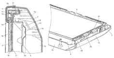
- FIG. 4 is a plan view of the liquid crystal display device from which a back cabinet is removed.
- FIG. 5 is a cross-sectional view of the liquid crystal display device taken along line 5 - 5 in FIG. 2 .
- FIG. 6 is an enlarged view of a portion B of the liquid crystal display device in FIG. 5 .
- FIG. 7 is an exploded perspective view of the liquid crystal display device.
- FIG. 8 is a perspective view of a back cabinet on an inner wall surface side of the liquid crystal display device.
- FIG. 9 is an exploded perspective view of a display module of the liquid crystal display device.
- FIG. 10 is an enlarged perspective view of main parts of the liquid crystal display device.
- FIG. 1 is a front view of a liquid crystal display device which is a display device according to an embodiment of the instant application
- FIG. 2 is a perspective view of the liquid crystal display device illustrating a state where the stand is detached
- FIG. 3 is a block diagram illustrating a circuit block of the entire configuration of the liquid crystal display device
- FIG. 4 is a plan view of the liquid crystal display device from which a back cabinet is removed
- FIG. 5 is a cross-sectional view of the liquid crystal display device taken along line 5 - 5 in FIG. 2
- FIG. 6 is an enlarged view of a portion B of the liquid crystal display device in FIG. 5
- FIG. 7 is an exploded perspective view of the liquid crystal display device.
- the liquid crystal display device includes display device main body 1 , and stand 2 which holds display device main body 1 in a standing state.
- Display device main body 1 is configured by accommodating a display 1 nodule having liquid crystal display panel 3 which is a flat display panel and backlight unit 4 (illustrated in FIG. 5 ) in casing 5 formed of a resin molded product.
- casing 5 includes front cabinet 6 which is provided with opening 6 a so as to correspond to an image display region of liquid crystal display panel 3 , and back cabinet 7 combined with front cabinet 6 .
- the reference numeral 6 b indicates a speaker grill for emitting the sound of a speaker to outside.
- a schematic configuration of the entire liquid crystal display device includes a signal processing circuit block 8 which has a driving circuit displaying an image on liquid crystal display panel 3 and a lighting control circuit controlling lighting of the backlight unit 4 , power supply block 9 which supplies power to liquid crystal display panel 3 , backlight unit 4 , and signal processing circuit block 8 , tuner 10 which receives television broadcasting and supplies a received signal to the signal processing circuit block 8 , and speaker 11 which outputs sound.
- Signal processing circuit block 8 and power supply block 9 respectively have components forming circuits mounted on circuit boards. Further, a circuit board which has signal processing circuit block 8 , power supply block 9 , tuner 10 , and the like mounted thereon is installed so as to be disposed in a space between a back face of backlight unit 4 and back cabinet 7 .
- signal processing circuit block 8 is equipped with external signal input terminals 12 used to input a video signal from an external device such as a DVD player to the liquid crystal display device. Further, a speaker is not illustrated in FIG. 3 .
- back cabinet 7 has a space 7 a in which the display module including liquid crystal display panel 3 and backlight unit 4 , and the circuit board can be accommodated. Further, an inner bottom surface forming space 7 a is provided with backlight supporters 7 b and 7 c supporting backlight unit 4 . Of backlight supporters 7 b and 7 c , frame 4 a of backlight unit 4 is installed at backlight supporter 7 b using screw 13 .
- panel supporter 7 d which is a resin molded product that supports an outer circumference of liquid crystal display panel 3 and holds panel supporting member 14 is provided in the circumference of the inner bottom surface of back cabinet 7 .
- the outer circumference of liquid crystal display panel 3 is supported by panel supporting member 14 .
- the outer circumference of liquid crystal display panel 3 is pressed against panel supporting member 14 by frame 15 which is made of metal and has a cross-sectional shape of a substantially L shape. By this pressing, liquid crystal display panel 3 is accommodated and disposed in the opening circumference of space 7 a of back cabinet 7 .
- the reference numeral 3 a indicates a polarization film attached to a display surface of liquid crystal display panel 3 .
- liquid crystal display panel 3 disposed in the opening of space 7 a of back cabinet 7 is electrically connected to the circuit board corresponding to signal processing circuit block 8 disposed on the back side of backlight unit 4 via a flexible wire board corresponding to a wire member which is disposed along the outer circumference of backlight unit 4 . A detailed structure thereof will be described later.
- FIG. 6 outer circumferential front end 7 e of back cabinet 7 is fitted to fitting piece 6 c provided on the inner circumferential wall surface of front cabinet 6 .
- front cabinet 6 is installed in back cabinet 7 using screws from the front cabinet 6 side, and thereby the circuit board having the display module and the driving circuits thereon is accommodated in the casing.
- FIG. 8 is a perspective view of the back cabinet of the inner wall surface side of the liquid crystal display device, and front cabinet 6 is installed at bosses 7 f provided in the outer circumference of back cabinet 7 using screws.
- FIG. 9 is an exploded perspective view of the display module of the liquid crystal display device.
- backlight unit 4 illuminates liquid crystal display panel 3 from the back side.
- Backlight unit 4 includes a plurality of linear light sources 16 arranged in parallel to liquid crystal display panel 3 in frame 4 a and diffusion plate 17 covering frame 4 a.
- Optical sheet 18 such as a prism sheet which diffuses or collects light passing through diffusion plate 17 is laminated on diffusion plate 17 .
- Reflection sheet 19 which is formed of a metal foil and reflects light emitted from linear light sources 16 toward diffusion plate 17 is disposed on the inner bottom surface of frame 4 a so as to entirely cover the inner bottom surface.
- a pair of supporting members 20 which are spaced apart from each other in the extending direction of the linear light sources 16 and hold linear light sources 16 are disposed.
- linear light sources 16 tubular cold cathode fluorescent lamps (CCFLs) are used and are arranged in parallel to each other.
- both ends of linear light sources 16 are covered by supporting members 20 .
- frame 4 a is made of metal, such as iron or aluminum, or resin.
- Frame 4 a has a box shape which is open in one direction, and has a bottom wall forming a bottom surface parallel to the arranged surface of linear light sources 16 and a side wall rising from the circumference of the bottom wall. Furthermore, a plurality of diffusion plate supporting members 21 supporting diffusion plate 17 are disposed on the inner bottom surface of frame 4 a.
- Diffusion plate 17 is disposed between linear light sources 16 and liquid crystal display panel 3 .
- Diffusion plate 17 makes light which is incident from an incidence surface of linear light sources 16 side diffused so as to be emitted from an exit surface of the liquid crystal display panel 3 side, and is formed through injecting molding of a transparent resin such as polystyrene or polycarbonate.
- diffusion plate 17 is disposed opposite to reflection sheet 19 with linear light sources 16 interposed therebetween.
- This diffusion plate 17 has an incidence surface which makes direct light from linear light sources 16 and reflected light from reflection sheet 19 incident to the inside thereof and an exit surface which emits light diffused in the inside.
- optical sheet 18 disposed so as to be laminated on the exit surface.
- FIG. 10 is an enlarged perspective view of the main parts of the liquid crystal display device.
- panel driving circuit board 22 for electrically connecting liquid crystal display panel 3 to the circuit board of the signal processing circuit block 8 disposed on the back side of backlight unit 4 panel driving circuit board 22 is electrically connected to liquid crystal display panel 3 via a flexible wire board 24 .
- notches are provided at the side wall of back cabinet 7 corresponding to connector 23 such that connectors 23 between flexible wire board 24 and panel driving circuit board 22 are exposed to outside from side wall 7 g of back cabinet 7 .
- liquid crystal display panel 3 can be easily connected to panel driving circuit board 22 when assembly is performed.
- connection portions between the circuit board of signal processing circuit block 8 and panel driving circuit board 22 may be configured to be exposed to outside from side wall 7 g of back cabinet 7 .
- back cabinet 7 has space 7 a which can accommodate backlight unit 4 and the circuit board, backlight supporters 7 b and 7 c supporting backlight unit 4 are provided on the inner wall surface forming space 7 a , liquid crystal display panel 3 is disposed in the opening of space 7 a of back cabinet 7 , and connectors 23 between liquid crystal display panel 3 and panel driving circuit board 22 are exposed to outside from side wall 7 g of back cabinet 7 .
- backlight unit 4 and liquid crystal display panel 3 are sequentially incorporated into back cabinet 7 with respect to back cabinet 7 , and thereby a finished product can be assembled.
- the display module including backlight unit 4 and liquid crystal display panel 3 is assembled, and assembly is easier than in a case where a circuit board having liquid crystal display panel 3 and driving circuits of the backlight unit mounted thereon is installed and is then accommodated in the casing.
- liquid crystal display panel 3 and panel driving circuit board 22 are exposed to the outside from side wall 7 g of back cabinet 7 , and thus liquid crystal display panel 3 can be easily connected to flexible wire board 24 when assembly is performed.
Abstract
Back cabinet has space which can accommodate backlight unit and a circuit board therein, a backlight supporter which supports backlight unit is provided on an inner wall surface forming space, liquid crystal display panel is disposed in an opening of space of back cabinet, and panel driving circuit board for electrically connecting liquid crystal display panel to a signal processing circuit board is exposed to outside from a side wall of back cabinet.
Description
This application is a continuation application of U.S. application Ser. No. 13/676,500, filed on Nov. 14, 2012, which is a continuation application of International Application No. PCT/JP2011/005332, filed on Sep. 22, 2011, which in turn claims the benefit of Japanese Application No. 2010-216445, filed on Sep. 28, 2010, the disclosures of which Applications are incorporated by reference herein.
The instant application relates to a flat display device such as a liquid crystal display device used for a television receiver or a monitor device.
A liquid crystal display device is a flat display device, and demands thereof have increased for general homes and business use.
Generally, the liquid crystal display device includes a display module which is configured by disposing a backlight unit which is a surface light source on a back surface side of a flat liquid crystal display panel, and the display module is accommodated inside a thin casing including a front cabinet and a back cabinet (refer to PTL 1)
In addition, the liquid crystal display device is produced as follows by a panel manufacturer and a finished product manufacturer.
The panel manufacturer manufactures liquid crystal display panels which are supplied to the finished product manufacturer such as a television manufacturer.
The finished product manufacturer combines a backlight unit which is a surface light source with the liquid crystal display panel, thereby manufacturing a display module. In addition, the display module is accommodated in a thin casing including a front cabinet and a back cabinet along with a driving circuit board of the liquid crystal display panel.
In this way, the liquid crystal display device is produced.
In addition, a finished product manufacturer builds a factory for assembling products at an area in which liquid crystal display device are sold or an area close to the area, and finished products having designs and functions corresponding to the sales area are assembled and sold.
Along with the increase in demand for liquid crystal display devices in the whole world, there are requests for reduction in the number of assembling steps when a finished product is assembled and for ease of assembly, and there is a request for simplicity of a packaging method in a case of transporting display modules or the like to a factory for performing assembly.
- PTL 1: Unexamined Japanese Patent Publication No. 2009-139426
According to the instant application, a display device includes a casing having a back cabinet; a flat display panel installed in the casing; a backlight unit disposed on a back side of the flat display panel; a circuit board forming a driving circuit for displaying an image on the flat display panel; and a wire member electrically connecting the circuit board to the flat display panel, wherein the back cabinet has a space which can accommodate the backlight unit and the circuit board therein, and a backlight supporter which supports the backlight unit on an inner wall surface forming the space, and wherein the flat display panel is disposed in an opening of the space of the back cabinet, and a connector between the flat display panel and the wire member is exposed to the outside from a side wall of the back cabinet.
Hereinafter, a display device according to an embodiment of the instant application will be described with reference to the drawings by exemplifying a liquid crystal display device.
First, as illustrated in FIGS. 1 and 2 , the liquid crystal display device includes display device main body 1, and stand 2 which holds display device main body 1 in a standing state. Display device main body 1 is configured by accommodating a display 1 nodule having liquid crystal display panel 3 which is a flat display panel and backlight unit 4 (illustrated in FIG. 5 ) in casing 5 formed of a resin molded product. In addition, casing 5 includes front cabinet 6 which is provided with opening 6 a so as to correspond to an image display region of liquid crystal display panel 3, and back cabinet 7 combined with front cabinet 6. In addition, the reference numeral 6 b indicates a speaker grill for emitting the sound of a speaker to outside.
In addition, as illustrated in FIGS. 3 and 4 , a schematic configuration of the entire liquid crystal display device includes a signal processing circuit block 8 which has a driving circuit displaying an image on liquid crystal display panel 3 and a lighting control circuit controlling lighting of the backlight unit 4, power supply block 9 which supplies power to liquid crystal display panel 3, backlight unit 4, and signal processing circuit block 8, tuner 10 which receives television broadcasting and supplies a received signal to the signal processing circuit block 8, and speaker 11 which outputs sound. Signal processing circuit block 8 and power supply block 9 respectively have components forming circuits mounted on circuit boards. Further, a circuit board which has signal processing circuit block 8, power supply block 9, tuner 10, and the like mounted thereon is installed so as to be disposed in a space between a back face of backlight unit 4 and back cabinet 7.
In addition, as illustrated in FIG. 4 , signal processing circuit block 8 is equipped with external signal input terminals 12 used to input a video signal from an external device such as a DVD player to the liquid crystal display device. Further, a speaker is not illustrated in FIG. 3 . Here, as illustrated in FIGS. 5 to 7 , back cabinet 7 has a space 7 a in which the display module including liquid crystal display panel 3 and backlight unit 4, and the circuit board can be accommodated. Further, an inner bottom surface forming space 7 a is provided with backlight supporters 7 b and 7 c supporting backlight unit 4. Of backlight supporters 7 b and 7 c, frame 4 a of backlight unit 4 is installed at backlight supporter 7 b using screw 13.
Further, panel supporter 7 d which is a resin molded product that supports an outer circumference of liquid crystal display panel 3 and holds panel supporting member 14 is provided in the circumference of the inner bottom surface of back cabinet 7. In addition, the outer circumference of liquid crystal display panel 3 is supported by panel supporting member 14. The outer circumference of liquid crystal display panel 3 is pressed against panel supporting member 14 by frame 15 which is made of metal and has a cross-sectional shape of a substantially L shape. By this pressing, liquid crystal display panel 3 is accommodated and disposed in the opening circumference of space 7 a of back cabinet 7. In addition, the reference numeral 3 a indicates a polarization film attached to a display surface of liquid crystal display panel 3.
Here, liquid crystal display panel 3 disposed in the opening of space 7 a of back cabinet 7 is electrically connected to the circuit board corresponding to signal processing circuit block 8 disposed on the back side of backlight unit 4 via a flexible wire board corresponding to a wire member which is disposed along the outer circumference of backlight unit 4. A detailed structure thereof will be described later.
In addition, as illustrated in FIG. 6 , outer circumferential front end 7 e of back cabinet 7 is fitted to fitting piece 6 c provided on the inner circumferential wall surface of front cabinet 6. Further, front cabinet 6 is installed in back cabinet 7 using screws from the front cabinet 6 side, and thereby the circuit board having the display module and the driving circuits thereon is accommodated in the casing. FIG. 8 is a perspective view of the back cabinet of the inner wall surface side of the liquid crystal display device, and front cabinet 6 is installed at bosses 7 f provided in the outer circumference of back cabinet 7 using screws.
Specifically, as illustrated in FIG. 9 , diffusion plate 17 is disposed opposite to reflection sheet 19 with linear light sources 16 interposed therebetween. This diffusion plate 17 has an incidence surface which makes direct light from linear light sources 16 and reflected light from reflection sheet 19 incident to the inside thereof and an exit surface which emits light diffused in the inside.
The above-described optical sheet 18 IS disposed so as to be laminated on the exit surface.
With this configuration, liquid crystal display panel 3 can be easily connected to panel driving circuit board 22 when assembly is performed.
In addition, although, in the example illustrated in FIG. 10 , only connectors 23 between liquid crystal display panel 3 and panel driving circuit board 22 are configured to be exposed to the outside from side wall 7 g of back cabinet 7, connection portions between the circuit board of signal processing circuit block 8 and panel driving circuit board 22 may be configured to be exposed to outside from side wall 7 g of back cabinet 7.
As such, in the present embodiment, in the liquid crystal display device which includes the casing having back cabinet 7, liquid crystal display panel 3 and backlight unit 4 accommodated in the casing, and the circuit board forming the driving circuit for displaying an image on liquid crystal display panel 3, back cabinet 7 has space 7 a which can accommodate backlight unit 4 and the circuit board, backlight supporters 7 b and 7 c supporting backlight unit 4 are provided on the inner wall surface forming space 7 a, liquid crystal display panel 3 is disposed in the opening of space 7 a of back cabinet 7, and connectors 23 between liquid crystal display panel 3 and panel driving circuit board 22 are exposed to outside from side wall 7 g of back cabinet 7.
Thereby, backlight unit 4 and liquid crystal display panel 3 are sequentially incorporated into back cabinet 7 with respect to back cabinet 7, and thereby a finished product can be assembled. For this reason, the display module including backlight unit 4 and liquid crystal display panel 3 is assembled, and assembly is easier than in a case where a circuit board having liquid crystal display panel 3 and driving circuits of the backlight unit mounted thereon is installed and is then accommodated in the casing.
Further, connectors 23 between liquid crystal display panel 3 and panel driving circuit board 22 are exposed to the outside from side wall 7 g of back cabinet 7, and thus liquid crystal display panel 3 can be easily connected to flexible wire board 24 when assembly is performed.
Claims (4)
1. A display device comprising:
an outermost casing composed of a front cabinet and a back cabinet;
a flat display panel installed in the outermost casing;
a backlight unit disposed on a back side of the flat display panel;
a signal processing circuit board that controls an image signal output to the flat display panel, the signal processing circuit board being disposed on a back side of the backlight unit; and
a panel driving circuit board electrically connecting the signal processing circuit board to the flat display panel and controlling driving of the panel,
wherein the front cabinet is fixed to the back cabinet,
wherein the back cabinet has a space which accommodates the backlight unit and the signal processing circuit board therein, and a backlight supporter which supports the backlight unit on an inner wall surface forming the space,
wherein the flat display panel is disposed in an opening of the space of the back cabinet, and a connector between the flat display panel and the panel driving circuit board is exposed to outside from a side wall of the back cabinet when viewed from a side of the back cabinet without the front cabinet, and
wherein a connection portion between the signal processing circuit board and the panel driving circuit board is exposed to the outside from the side wall of the back cabinet when viewed from the side of the back cabinet without the front cabinet.
2. The display device of claim 1 , wherein
the front cabinet is fixed to the back cabinet with screws.
3. A method of assembling a display device, the display device comprising:
an outermost casing composed of a front cabinet and a back cabinet;
a flat display panel installed in the outermost casing;
a backlight unit disposed on a back side of the flat display panel;
a signal processing circuit board that controls an image signal output to the flat display panel; and
a panel driving circuit board electrically connecting the signal processing circuit board to the flat display panel and controlling driving of the panel,
the method comprising steps of:
putting the backlight unit in a space of the back cabinet, a backlight supporter which supports the backlight unit on an inner wall surface forming the space, the signal processing circuit board being disposed on a back side of the backlight unit;
putting the flat display panel in an opening of the space of the back cabinet;
connecting the flat display panel to the panel driving circuit board, a connector between the flat display panel and the panel driving circuit board being exposed to outside from a side wall of the back cabinet when viewed from a side of the back cabinet; and
fixing the front cabinet to the back cabinet.
4. The method of claim 3 , further comprising a step of:
connecting the signal processing circuit board to the panel driving circuit board, a connection portion between the signal processing circuit board and the panel driving circuit board being exposed to the outside from the side wall of the back cabinet when viewed from the side of the back cabinet before the front cabinet is fixed to the back cabinet.
Priority Applications (1)
| Application Number | Priority Date | Filing Date | Title |
|---|---|---|---|
| US15/239,403 US9646545B2 (en) | 2010-09-28 | 2016-08-17 | Display device |
Applications Claiming Priority (5)
| Application Number | Priority Date | Filing Date | Title |
|---|---|---|---|
| JP2010216445 | 2010-09-28 | ||
| JP2010-216445 | 2010-09-28 | ||
| PCT/JP2011/005332 WO2012042797A1 (en) | 2010-09-28 | 2011-09-22 | Display device |
| US13/676,500 US9443475B2 (en) | 2010-09-28 | 2012-11-14 | Display device |
| US15/239,403 US9646545B2 (en) | 2010-09-28 | 2016-08-17 | Display device |
Related Parent Applications (1)
| Application Number | Title | Priority Date | Filing Date |
|---|---|---|---|
| US13/676,500 Continuation US9443475B2 (en) | 2010-09-28 | 2012-11-14 | Display device |
Publications (2)
| Publication Number | Publication Date |
|---|---|
| US20160358555A1 US20160358555A1 (en) | 2016-12-08 |
| US9646545B2 true US9646545B2 (en) | 2017-05-09 |
Family
ID=45892289
Family Applications (2)
| Application Number | Title | Priority Date | Filing Date |
|---|---|---|---|
| US13/676,500 Expired - Fee Related US9443475B2 (en) | 2010-09-28 | 2012-11-14 | Display device |
| US15/239,403 Expired - Fee Related US9646545B2 (en) | 2010-09-28 | 2016-08-17 | Display device |
Family Applications Before (1)
| Application Number | Title | Priority Date | Filing Date |
|---|---|---|---|
| US13/676,500 Expired - Fee Related US9443475B2 (en) | 2010-09-28 | 2012-11-14 | Display device |
Country Status (4)
| Country | Link |
|---|---|
| US (2) | US9443475B2 (en) |
| JP (1) | JP5877318B2 (en) |
| CN (1) | CN103003859B (en) |
| WO (1) | WO2012042797A1 (en) |
Families Citing this family (5)
| Publication number | Priority date | Publication date | Assignee | Title |
|---|---|---|---|---|
| KR102145892B1 (en) * | 2014-01-22 | 2020-08-19 | 엘지전자 주식회사 | Display Apparatus |
| CN104144308B (en) * | 2014-07-28 | 2017-04-05 | 深圳创维-Rgb电子有限公司 | A kind of LCD TV housing of LCD TV and its compatible plane screen and cambered surface screen |
| JP6198910B1 (en) * | 2016-03-18 | 2017-09-20 | シャープ株式会社 | Display device and television receiver |
| WO2017159111A1 (en) * | 2016-03-18 | 2017-09-21 | シャープ株式会社 | Display device and television receiver |
| KR102504803B1 (en) * | 2016-04-06 | 2023-02-28 | 엘지전자 주식회사 | Display device |
Citations (17)
| Publication number | Priority date | Publication date | Assignee | Title |
|---|---|---|---|---|
| JP2001109390A (en) | 1999-08-04 | 2001-04-20 | Sanyo Electric Co Ltd | Display device |
| JP2004126287A (en) | 2002-10-03 | 2004-04-22 | Nec Kagoshima Ltd | Liquid crystal display and its manufacturing method |
| US20040109104A1 (en) | 2002-12-04 | 2004-06-10 | Lee Sang-Duk | Flat panel display device |
| US20050018102A1 (en) | 2003-06-24 | 2005-01-27 | Yoshihisa Hirano | Electrooptic device, method for manufacturing same, and electronic apparatus |
| US20050052587A1 (en) | 2003-09-10 | 2005-03-10 | Hitachi Displays, Ltd. | Display device |
| CN1598660A (en) | 2003-09-19 | 2005-03-23 | 精工爱普生株式会社 | Electrooptical device,electronic device and manufacturing method of electrooptical device |
| CN1697996A (en) | 2002-11-14 | 2005-11-16 | 松下电器产业株式会社 | Lcd |
| CN1749830A (en) | 2004-09-17 | 2006-03-22 | 三洋电机株式会社 | Liquid crystal display device and a mobile information terminal including a liquid crystal display device |
| US20060119761A1 (en) | 2004-11-30 | 2006-06-08 | Tatsumi Okuda | Display and mobile device |
| US20060170839A1 (en) | 2005-01-26 | 2006-08-03 | Sanyo Epson Imaging Devices Corp. | Display module |
| US20070133158A1 (en) | 2005-12-14 | 2007-06-14 | Orion Electric Co., Ltd. | Display device |
| US20080079864A1 (en) | 2006-09-28 | 2008-04-03 | Nec Lcd Technologies, Ltd. | Liquid crystal panel module and liquid crystal display device using the same |
| US20080291356A1 (en) | 2007-05-25 | 2008-11-27 | Tae Seok Kim | Backlight assembly and liquid crystal display having the same |
| JP2008310181A (en) | 2007-06-15 | 2008-12-25 | Sharp Corp | Thin display device |
| US20090140963A1 (en) | 2007-12-03 | 2009-06-04 | Sanyo Electric Co., Ltd. | Image display device |
| JP2009151112A (en) | 2007-12-20 | 2009-07-09 | Sharp Corp | Liquid crystal display device and assembling method of liquid crystal display device |
| CN103201782A (en) | 2011-02-22 | 2013-07-10 | 松下电器产业株式会社 | Method for producing display device |
-
2011
- 2011-09-22 JP JP2012536184A patent/JP5877318B2/en not_active Expired - Fee Related
- 2011-09-22 WO PCT/JP2011/005332 patent/WO2012042797A1/en active Application Filing
- 2011-09-22 CN CN201180035198.1A patent/CN103003859B/en not_active Expired - Fee Related
-
2012
- 2012-11-14 US US13/676,500 patent/US9443475B2/en not_active Expired - Fee Related
-
2016
- 2016-08-17 US US15/239,403 patent/US9646545B2/en not_active Expired - Fee Related
Patent Citations (27)
| Publication number | Priority date | Publication date | Assignee | Title |
|---|---|---|---|---|
| JP2001109390A (en) | 1999-08-04 | 2001-04-20 | Sanyo Electric Co Ltd | Display device |
| US20040160547A1 (en) | 2002-10-03 | 2004-08-19 | Nec Lcd Technologies, Ltd. | LCD device having a reduced number of components |
| JP2004126287A (en) | 2002-10-03 | 2004-04-22 | Nec Kagoshima Ltd | Liquid crystal display and its manufacturing method |
| CN1697996A (en) | 2002-11-14 | 2005-11-16 | 松下电器产业株式会社 | Lcd |
| US20060152101A1 (en) | 2002-11-14 | 2006-07-13 | Hiroshi Nagahama | Liquid crystal display |
| US20040109104A1 (en) | 2002-12-04 | 2004-06-10 | Lee Sang-Duk | Flat panel display device |
| US20050018102A1 (en) | 2003-06-24 | 2005-01-27 | Yoshihisa Hirano | Electrooptic device, method for manufacturing same, and electronic apparatus |
| CN1573454A (en) | 2003-06-24 | 2005-02-02 | 精工爱普生株式会社 | Electrooptic device, method for manufacturing same, and electronic apparatus |
| US20050052587A1 (en) | 2003-09-10 | 2005-03-10 | Hitachi Displays, Ltd. | Display device |
| CN1598660A (en) | 2003-09-19 | 2005-03-23 | 精工爱普生株式会社 | Electrooptical device,electronic device and manufacturing method of electrooptical device |
| US20050094052A1 (en) | 2003-09-19 | 2005-05-05 | Shinji Sakurai | Electro-optical device, electronic apparatus, and method of producing electro-optical device |
| CN1749830A (en) | 2004-09-17 | 2006-03-22 | 三洋电机株式会社 | Liquid crystal display device and a mobile information terminal including a liquid crystal display device |
| US20060061704A1 (en) | 2004-09-17 | 2006-03-23 | Satoshi Hayano | Liquid crystal display device and a mobile information terminal including a liquid crystal display device |
| US20060119761A1 (en) | 2004-11-30 | 2006-06-08 | Tatsumi Okuda | Display and mobile device |
| CN1811543A (en) | 2004-11-30 | 2006-08-02 | 三洋电机株式会社 | Display and mobile device |
| US20060170839A1 (en) | 2005-01-26 | 2006-08-03 | Sanyo Epson Imaging Devices Corp. | Display module |
| US20070133158A1 (en) | 2005-12-14 | 2007-06-14 | Orion Electric Co., Ltd. | Display device |
| JP2007163861A (en) | 2005-12-14 | 2007-06-28 | Orion Denki Kk | Display apparatus |
| US20080079864A1 (en) | 2006-09-28 | 2008-04-03 | Nec Lcd Technologies, Ltd. | Liquid crystal panel module and liquid crystal display device using the same |
| JP2008083584A (en) | 2006-09-28 | 2008-04-10 | Nec Lcd Technologies Ltd | Liquid crystal panel module and liquid crystal display device |
| US20080291356A1 (en) | 2007-05-25 | 2008-11-27 | Tae Seok Kim | Backlight assembly and liquid crystal display having the same |
| JP2008310181A (en) | 2007-06-15 | 2008-12-25 | Sharp Corp | Thin display device |
| US20090140963A1 (en) | 2007-12-03 | 2009-06-04 | Sanyo Electric Co., Ltd. | Image display device |
| JP2009139426A (en) | 2007-12-03 | 2009-06-25 | Sanyo Electric Co Ltd | Image display device |
| JP2009151112A (en) | 2007-12-20 | 2009-07-09 | Sharp Corp | Liquid crystal display device and assembling method of liquid crystal display device |
| CN103201782A (en) | 2011-02-22 | 2013-07-10 | 松下电器产业株式会社 | Method for producing display device |
| US20130192055A1 (en) | 2011-02-22 | 2013-08-01 | Panasonic Corporation | Method for producing display device |
Non-Patent Citations (7)
| Title |
|---|
| English Translation of Chinese Search Report dated Feb. 6, 2015 for the related Chinese Patent Application No. 201180035198.1. |
| International Search Report mailed Dec. 20, 2011 issued in corresponding International Application No. PCT/JP20111/005332. |
| U.S. Notice of Allowance issued in U.S Appl. No. 13/676,500 dated Aug. 23, 2016. |
| U.S. Office Action issued in U.S. Appl. No. 13/676,500 dated Apr. 2, 2015. |
| U.S. Office Action issued in U.S. Appl. No. 13/676,500 dated Jul. 28, 2015. |
| U.S. Office Action issued in U.S. Appl. No. 13/676,500 dated Jun. 16, 2014. |
| U.S. Office Action issued in U.S. Appl. No. 13/676,500 dated Nov. 4, 2014. |
Also Published As
| Publication number | Publication date |
|---|---|
| JP5877318B2 (en) | 2016-03-08 |
| JPWO2012042797A1 (en) | 2014-02-03 |
| US9443475B2 (en) | 2016-09-13 |
| US20160358555A1 (en) | 2016-12-08 |
| WO2012042797A1 (en) | 2012-04-05 |
| CN103003859B (en) | 2015-07-22 |
| CN103003859A (en) | 2013-03-27 |
| US20130069856A1 (en) | 2013-03-21 |
Similar Documents
| Publication | Publication Date | Title |
|---|---|---|
| US9646545B2 (en) | Display device | |
| KR101569154B1 (en) | Liquid crystal display and television apparatus having the same | |
| US10884276B2 (en) | Display device with simplified appearance structure and improved coupling arrangement | |
| EP2339426B1 (en) | Display apparatus | |
| EP2337343B1 (en) | Display apparatus and assembly for forming a display apparatus | |
| US8310627B2 (en) | Display device and television receiver apparatus | |
| US7869197B2 (en) | Display apparatus | |
| JP2004077955A (en) | Liquid crystal display device | |
| US8970793B2 (en) | Display device, and television device | |
| KR101007048B1 (en) | Backlight unit for dual faces lighting display device | |
| WO2012042799A1 (en) | Display device | |
| WO2012042798A1 (en) | Display device | |
| WO2012114701A1 (en) | Method for producing display device | |
| KR101014425B1 (en) | Dual faces lighting display device | |
| CN116125703A (en) | Display device, backlight module and assembling method of backlight module | |
| KR100980844B1 (en) | Drive device for dual faces lighting display device | |
| US20150355504A1 (en) | Image display apparatus | |
| CN111246141B (en) | Pickup box body of television | |
| CN109167947B (en) | Novel assembly structure of TV set | |
| JPH10240153A (en) | Liquid crystal display device | |
| US20140185200A1 (en) | Display apparatus | |
| KR20110089531A (en) | Dispaly module and dispaly apparatus thereof | |
| JP2013050649A (en) | Display device |
Legal Events
| Date | Code | Title | Description |
|---|---|---|---|
| STCF | Information on status: patent grant |
Free format text: PATENTED CASE |
|
| FEPP | Fee payment procedure |
Free format text: MAINTENANCE FEE REMINDER MAILED (ORIGINAL EVENT CODE: REM.); ENTITY STATUS OF PATENT OWNER: LARGE ENTITY |
|
| LAPS | Lapse for failure to pay maintenance fees |
Free format text: PATENT EXPIRED FOR FAILURE TO PAY MAINTENANCE FEES (ORIGINAL EVENT CODE: EXP.); ENTITY STATUS OF PATENT OWNER: LARGE ENTITY |
|
| STCH | Information on status: patent discontinuation |
Free format text: PATENT EXPIRED DUE TO NONPAYMENT OF MAINTENANCE FEES UNDER 37 CFR 1.362 |
|
| FP | Lapsed due to failure to pay maintenance fee |
Effective date: 20210509 |