US9640677B2 - Solar cell, solar cell module - Google Patents
Solar cell, solar cell module Download PDFInfo
- Publication number
- US9640677B2 US9640677B2 US14/546,523 US201414546523A US9640677B2 US 9640677 B2 US9640677 B2 US 9640677B2 US 201414546523 A US201414546523 A US 201414546523A US 9640677 B2 US9640677 B2 US 9640677B2
- Authority
- US
- United States
- Prior art keywords
- finger
- portions
- solar cell
- tip end
- finger portions
- Prior art date
- Legal status (The legal status is an assumption and is not a legal conclusion. Google has not performed a legal analysis and makes no representation as to the accuracy of the status listed.)
- Active
Links
Images


Classifications
-
- H—ELECTRICITY
- H10—SEMICONDUCTOR DEVICES; ELECTRIC SOLID-STATE DEVICES NOT OTHERWISE PROVIDED FOR
- H10F—INORGANIC SEMICONDUCTOR DEVICES SENSITIVE TO INFRARED RADIATION, LIGHT, ELECTROMAGNETIC RADIATION OF SHORTER WAVELENGTH OR CORPUSCULAR RADIATION
- H10F77/00—Constructional details of devices covered by this subclass
- H10F77/20—Electrodes
- H10F77/206—Electrodes for devices having potential barriers
- H10F77/211—Electrodes for devices having potential barriers for photovoltaic cells
- H10F77/215—Geometries of grid contacts
-
- H01L31/022433—
-
- H01L31/022441—
-
- H01L31/0516—
-
- H—ELECTRICITY
- H10—SEMICONDUCTOR DEVICES; ELECTRIC SOLID-STATE DEVICES NOT OTHERWISE PROVIDED FOR
- H10F—INORGANIC SEMICONDUCTOR DEVICES SENSITIVE TO INFRARED RADIATION, LIGHT, ELECTROMAGNETIC RADIATION OF SHORTER WAVELENGTH OR CORPUSCULAR RADIATION
- H10F19/00—Integrated devices, or assemblies of multiple devices, comprising at least one photovoltaic cell covered by group H10F10/00, e.g. photovoltaic modules
- H10F19/90—Structures for connecting between photovoltaic cells, e.g. interconnections or insulating spacers
- H10F19/902—Structures for connecting between photovoltaic cells, e.g. interconnections or insulating spacers for series or parallel connection of photovoltaic cells
- H10F19/908—Structures for connecting between photovoltaic cells, e.g. interconnections or insulating spacers for series or parallel connection of photovoltaic cells for back-contact photovoltaic cells
-
- H—ELECTRICITY
- H10—SEMICONDUCTOR DEVICES; ELECTRIC SOLID-STATE DEVICES NOT OTHERWISE PROVIDED FOR
- H10F—INORGANIC SEMICONDUCTOR DEVICES SENSITIVE TO INFRARED RADIATION, LIGHT, ELECTROMAGNETIC RADIATION OF SHORTER WAVELENGTH OR CORPUSCULAR RADIATION
- H10F77/00—Constructional details of devices covered by this subclass
- H10F77/20—Electrodes
- H10F77/206—Electrodes for devices having potential barriers
- H10F77/211—Electrodes for devices having potential barriers for photovoltaic cells
- H10F77/219—Arrangements for electrodes of back-contact photovoltaic cells
-
- Y—GENERAL TAGGING OF NEW TECHNOLOGICAL DEVELOPMENTS; GENERAL TAGGING OF CROSS-SECTIONAL TECHNOLOGIES SPANNING OVER SEVERAL SECTIONS OF THE IPC; TECHNICAL SUBJECTS COVERED BY FORMER USPC CROSS-REFERENCE ART COLLECTIONS [XRACs] AND DIGESTS
- Y02—TECHNOLOGIES OR APPLICATIONS FOR MITIGATION OR ADAPTATION AGAINST CLIMATE CHANGE
- Y02E—REDUCTION OF GREENHOUSE GAS [GHG] EMISSIONS, RELATED TO ENERGY GENERATION, TRANSMISSION OR DISTRIBUTION
- Y02E10/00—Energy generation through renewable energy sources
- Y02E10/50—Photovoltaic [PV] energy
- Y02E10/547—Monocrystalline silicon PV cells
Definitions
- This disclosure relates to a solar cell, and a solar cell module.
- Aback contact solar cell has both of a p-side electrode and an n-side electrode on the back surface of a photoelectric conversion body.
- a back contact solar cell has both of a p-side electrode and an n-side electrode provided on the back surface side.
- the solar cell and the wiring member need to be positioned relative to each other with high positioning accuracy. For this reason, a back contact solar cell has a problem of being difficult to be connected to a wiring member.
- a solar cell includes a photoelectric conversion body, a first electrode, a second electrode, a first insulating layer, and a second insulating layer.
- the first electrode includes a first finger portion.
- the first finger portion is placed on one main surface of the photoelectric conversion body.
- the first finger portion extends in first direction.
- the second electrode includes a second finger portion.
- the second finger portion is placed on the one main surface of the photoelectric conversion body.
- the second finger portion is placed to be adjacent to the first finger portion in second direction intersecting the first direction.
- the second finger portion extends in the first direction.
- the first insulating layer covers at least part of a tip end portion of the first finger portion, which tip end portion is located on first side in the first direction.
- the second insulating layer covers at least part of a tip end portion of the second finger portion, which tip end portion is located on second side in the first direction.
- a solar cell module includes the solar cell described above and a wiring member electrically connected to the solar cell.
- a first lower electrode layer and a second lower electrode layer are formed on one main surface of a photoelectric conversion body, the first lower electrode layer extending in first direction, the second lower electrode layer extending in the first direction and being adjacent to the first lower electrode layer in the second direction intersecting the first direction.
- a first insulating layer is formed such that the first insulating layer covers at least part of a tip end portion of the first lower electrode layer, which tip end portion is located on first side in the first direction
- a second insulating layer is formed such that the second insulating layer covers at least part of a tip end portion of the second lower electrode layer, which tip end portion is located on a second side in the first direction.
- a first upper electrode layer is formed on a portion of the first lower electrode layer, which portion is not covered by the first insulating layer, to obtain a first electrode including a first finger portion including the first lower electrode layer and the first upper electrode layer.
- a second upper electrode layer is formed on a portion of the second lower electrode layer, which portion is not covered by the second insulating layer, to obtain a second electrode including a second finger portion including the second lower electrode layer and the second upper electrode layer.
- Multiple solar cells are fabricated in this way. The multiple solar cells are electrically connected together with a wiring member.
- FIG. 1 is a schematic diagram of the back surface of a solar cell according to one embodiment.
- FIG. 2 is a schematic sectional diagram taken along line II-II in FIG. 1 .
- FIG. 3 is a schematic sectional diagram taken along line III-III in FIG. 2 .
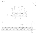
- FIG. 4 is a schematic sectional diagram of a solar cell module according to one embodiment.
- FIG. 5 is a schematic plan view illustrating how a wiring member is connected to the solar cells according to the one embodiment.
- FIG. 6 is a schematic sectional diagram taken along line VI-VI in FIG. 5 .
- FIG. 7 is a schematic diagram of the back surface of a solar cell according to a modification.
- FIG. 8 is a schematic plan view illustrating how a wiring member is connected to the solar cells according to the modification.
- solar cell 20 includes photoelectric conversion body 25 .
- Photoelectric conversion body 25 is not particularly limited as long as it is a member configured to generate carriers such as electrons and holes by receiving light.
- Photoelectric conversion body 25 may include, for example, a semiconductor substrate of one conductivity type, a first semiconductor layer of another conductivity type placed on one main surface of the semiconductor substrate, and a second semiconductor layer of the one conductivity type placed on the one main surface of the semiconductor substrate in at least part of a portion where the first semiconductor layer is not placed.
- a p-type surface is formed by the surface of one of the first and second semiconductor layers
- an n-type surface is formed by the surface of the other one.
- a substantially intrinsic i-type semiconductor layer may be placed between the semiconductor substrate and each of the first and second semiconductor layers, the i-type semiconductor layer having a thickness substantially not contributing to power generation, e.g., about several angstroms ( ⁇ ) to 250 ⁇ .
- Photoelectric conversion body 25 may be formed of, for example, a semiconductor substrate provided with a p-type dopant diffusion region and an n-type dopant diffusion region, each being exposed on the one main surface.
- first and second electrodes 21 and 22 are placed on main surface 25 a of photoelectric conversion body 25 .
- one of first and second electrodes 21 and 22 is provided on the p-type surface and forms a p-side electrode for collecting holes, and the other one is provided on the n-type surface and forms an n-side electrode for collecting electrons.
- First electrode 21 has multiple first finger portions 21 a and first bus bar portion 21 b .
- Multiple first finger portions 21 a are arranged with spaces in between in a y-axis direction which intersects an x-axis direction.
- Multiple first finger portions 21 a each extend in the x-axis direction.
- Multiple first finger portions 21 a are electrically connected to first bus bar portion 21 b .
- First bus bar portion 21 b is placed on an x1 side of multiple first finger portions 21 a .
- First bus bar portion 21 b extends in the y-axis direction.
- Second electrode 22 has multiple second finger portions 22 a and second bus bar portion 22 b .
- Multiple second finger portions 22 a are arranged with spaces in between in the y-axis direction.
- Multiple second finger portions 22 a each extend in the x-axis direction.
- Multiple second finger portions 22 a are electrically connected to second bus bar portion 22 b .
- Second bus bar portion 22 b is placed on an x2 side of multiple second finger portions 22 a .
- Second bus bar portion 22 b extends in the y-axis direction.
- Second finger portions 22 a and first finger portions 21 a interdigitate and are provided alternately in the y-axis direction.
- first finger portions 21 a and second finger portions 22 a are adjacent to each other in the y-axis direction.
- Each first finger portion 21 a is placed between two second finger portions 22 a .
- Each second finger portion 22 a is placed between two first finger portions 21 a.
- first finger portions 21 a on the opposite side from first bus bar portion 21 b face second bus bar portion 22 b in the x-axis direction.
- Tip end portions of second finger portions 22 a on the opposite side from second bus bar portion 22 b face first bus bar portion 21 b in the x-axis direction.
- first and second electrodes 21 and 22 has a bus bar portion in this embodiment, the first and second electrodes in the invention do not have to have the bus bar portions.
- First and second electrodes 21 and 22 can be formed from any appropriate conductive material.
- First and second electrodes 21 and 22 can be formed from, for example, at least one of metals such as silver, aluminum, copper, and tin.
- First and second electrodes 21 and 22 are each formed of a stack of conductive layers. Specifically, as illustrated in FIGS. 2 and 3 , first electrode 21 has first lower electrode layer 21 A and first upper electrode layer 21 B. Second electrode 22 has second lower electrode layer 22 A and second upper electrode layer 22 B.
- First and second lower electrode layers 21 A and 22 A are each provided on main surface 25 a of photoelectric conversion body 25 .
- First and second lower electrode layers 21 A and 22 A are each a layer formed by CVD (Chemical Vapor Deposition), sputtering, or other method.
- First upper electrode layer 21 B is placed on first lower electrode layer 21 A.
- First upper electrode layer 21 B is formed by plating using first lower electrode layer 21 A as a seed electrode.
- first upper electrode layer 21 B is placed on the substantially entire portion of first lower electrode layer 21 A, excluding the x2-side tip end portions of the portions of first lower electrode layer 21 A which form first finger portions 21 a .
- the x2-side tip end portions of first finger portions 21 a are thinner than other portions of first finger portions 21 a by an amount corresponding to the thickness of first upper electrode layer 21 B.
- Second upper electrode layer 22 B is placed on second lower electrode layer 22 A.
- Second upper electrode layer 22 B is formed by plating using second lower electrode layer 22 A as a seed electrode.
- second upper electrode layer 22 B is placed on the substantially entire portion of second lower electrode layer 22 A, excluding the x1-side tip end portions of the portions of second upper electrode layer 22 B which form second finger portions 22 a .
- the x1-side tip end portions of second finger portions 22 a are thinner than other portions of second finger portions 22 a by an amount corresponding to the thickness of second upper electrode layer 22 B.
- First lower electrode layer 21 A and second lower electrode layer 22 A have substantially the same thickness.
- the tip end portions of first finger portions 21 a on the x2 side in the x-axis direction are smaller than tip end portions of second finger portions 22 a on the x2 side in the x-axis direction.
- the tip end portions of second finger portions 22 a on the x1 side in the x-axis direction are smaller than tip end portions of first finger portions 21 a on the x1 side in the x-axis direction.
- first insulating layer 23 covers substantially the entire tip end portion of each first finger portion 21 a on the x2 side in the x-axis direction. Note that the part of first finger portion 21 a covered by first insulating layer 23 is formed only of first lower electrode layer 21 A out of first lower electrode layer 21 A and first upper electrode layer 21 B.
- First insulating layer 23 is provided such that the total thickness of the tip end portion of first finger portion 21 a on the x2 side in the x-axis direction and first insulating layer 23 placed thereon is smaller than the thickness of the tip end portion of second finger portion 22 a on the x2 side in the x-axis direction.
- the total thickness of the tip end portion of first finger portion 21 a on the x2 side in the x-axis direction and first insulating layer 23 placed thereon is preferably smaller than or equal to, or more preferably 0.9 times or less of, the thickness of the tip end portion of second finger portion 22 a on the x2 side in the x-axis direction.
- second insulating layer 24 covers substantially the entire tip end portion of each second finger portion 22 a on the x1 side in the x-axis direction. Note that the part of second finger portion 22 a covered by second insulating layer 24 is formed only of second lower electrode layer 22 A out of second lower electrode layer 22 A and second upper electrode layer 22 B.
- Second insulating layer 24 is provided such that the total thickness of the tip end portion of second finger portion 22 a on the x1 side in the x-axis direction and second insulating layer 24 placed thereon is smaller than the thickness of the tip end portion of first finger portion 21 a on the x1 side in the x-axis direction.
- the total thickness of the tip end portion of second finger portion 22 a on the x1 side in the x-axis direction and second insulating layer 24 placed thereon is preferably smaller than or equal to, or more preferably 0.9 times or less of, the thickness of the tip end portion of first finger portion 21 a on the x1 side in the x-axis direction.
- First and second insulating layers 23 and 24 can be formed from any appropriate insulating material.
- first and second insulating layers 23 and 24 can be formed from an insulating resin, an inorganic oxide, or the like.
- resins preferably usable as a material for first and second insulating layers 23 and 24 include an epoxy resin, acrylic resin, a silicone resin, an olefin resin, an ethylene-vinyl acetate resin, and the like.
- inorganic oxides preferably usable as a material for first and second insulating layers 23 and 24 include Al 2 O 3 , SiN, SiO 2 , and the like.
- Solar cell module 1 illustrated in FIG. 4 includes solar cell 20 described above. Specifically, solar cell module 1 includes multiple solar cells 20 . Multiple solar cells 20 are placed within filler layer 13 filled between light-receiving-surface protection member 11 and back-surface-side protection member 12 .
- Light-receiving-surface protection member 11 and back-surface-side protection member 12 can be each formed of, for example, a glass plate, a resin plate, a resin sheet, or the like.
- Filler layer 13 can be formed from, for example, a crosslinkable resin such as an ethylene-vinyl acetate copolymer (EVA) resin or a non-crosslinkable resin such as a polyolefin resin.
- EVA ethylene-vinyl acetate copolymer
- each wiring member 30 has wiring-member main body 31 and conductive layer 32 .
- Wiring-member main body 31 is substantially rectangular.
- Wiring-member main body 31 is made of an insulating material.
- Wiring-member main body 31 can be formed from, for example, a resin.
- Conductive layer 32 is placed on a surface of wiring-member main body 31 on the solar cell 20 side.
- Wiring-member main body 31 electrically connects first electrode 21 of one of two solar cells 20 adjacent in the x direction to second electrode 22 of the other solar cell 20 .
- Conductive layer 32 has multiple first connection portions 32 a , multiple second connection portions 32 b , and conductive-layer main body 32 c . Multiple first connection portions 32 a and multiple second connection portions 32 b are each electrically connected to conductive-layer main body 32 c.
- Multiple first connection portions 32 a extend from conductive-layer main body 32 c in the x-axis direction. Multiple first connection portions 32 a are arranged with spaces in between in the y-axis direction. Multiple first connection portions 32 a extend over to second finger portions 22 a . Multiple first connection portions 32 a are electrically connected to second bus bar portion 22 b and are also electrically connected to end portions of second finger portions 22 a on the second bus bar portion 22 b side.
- Multiple second connection portions 32 b extend from conductive-layer main body 32 c in the x-axis direction. Multiple second connection portions 32 b are arranged with spaces in between in the y-axis direction. Multiple second connection portions 32 b extend over to first finger portions 21 a . Multiple second connection portions 32 b are electrically connected to first bus bar portion 21 b and are also electrically connected to end portions of first finger portions 21 a on the first bus bar portion 21 b side.
- Resin adhesive layer 40 may be formed only from a hardened resin adhesive, but in this embodiment, includes hardened resin adhesive 41 and conductive material 42 .
- Conductive layer 32 and solar cell 20 are electrically connected to each other via this conductive material 42 .
- Conductive material 42 can be formed of, for example, particles of conductive material, insulating particles coated with a conductive layer, or the like.
- each first finger portion 21 a is covered with first insulating layer 23 .
- first insulating layer 23 At least part of the tip end portion of each first finger portion 21 a is covered with second insulating layer 24 .
- second insulating layer 24 At least part of the tip end portion of each second finger portion 22 a is covered with second insulating layer 24 .
- the maximum particle size of conductive material 42 should preferably be smaller than the thickness of each of first and second insulating layers 23 and 24 .
- the maximum particle size of conductive material 42 is preferably less than the thickness of each of first and second insulating layers 23 and 24 , and is more preferably less than or equal to two thirds of the thickness of each of first and second insulating layers 23 and 24 .
- first insulating layer 23 is provided to extend beyond conductive layer 32 to the x1 side in the x direction
- second insulating layer 24 is provided to extend beyond conductive layer 32 to the x2 side in the x direction.
- the total thickness of the x2-side tip end portion of first finger portion 21 a and first insulating layer 23 is smaller than the thickness of the x2-side tip end portion of second finger portion 22 a
- the total thickness of the x1-side tip end portion of second finger portion 22 a and second insulating layer 24 is smaller than the thickness of the x1-side tip end portion of first finger portion 21 a .
- first insulating layer 23 covers substantially the entire tip end portion of each first finger portion 21 a
- second insulating layer 24 covers substantially the entire tip end portion of second finger portion 22 a
- first insulating layer 23 may cover for example only edge portions of the x2-side tip end portion of first finger portion 21 a , the edge portions being adjacent to second finger portions 22 a
- second insulating layer 24 may cover for example only edge portions of the x1-side tip end portion of second finger portion 22 a , the edge portions being adjacent to first finger portions 21 a .
- the effect described above can be offered with such a configuration, as well.
- conductive layer 32 of wiring member 30 used in this embodiment is not limited to the one illustrated in FIG. 5 .
- conductive layer 32 may be substantially rectangular.
- first connection portions 32 a may be integrally provided, and second connection portions 32 b may be integrally provided.
- solar cell 20 can be manufactured by the following manufacturing method.
- first and second lower electrode layers 21 A and 22 A are formed on main surface 25 a of photoelectric conversion body 25 .
- First and second lower electrode layers 21 A and 22 A can be formed by, for example, CVD (Chemical Vapor Deposition), sputtering, or other method.
- First and second insulating layers 23 and 24 are formed.
- First and second insulating layers 23 and 24 can be formed by, for example, printing a resin material or sputtering an inorganic material.
- First and second insulating layers 23 and 24 may be formed also on a portion of main surface 25 a where first and second lower electrode layers 21 A and 22 A are not provided. In such a case, first insulating layer 23 and second insulating layer 24 may be provided to be integral with each other.
- first and second upper electrode layers 21 B and 22 B are formed on first and second lower electrode layers 21 A, 22 A.
- First and second electrodes 21 and 22 can be formed through the above steps.
- First and second upper electrode layers 21 B and 22 B can be formed by plating by feeding power to first and second lower electrode layers 21 A, 22 A.
Landscapes
- Photovoltaic Devices (AREA)
- Life Sciences & Earth Sciences (AREA)
- Engineering & Computer Science (AREA)
- Sustainable Development (AREA)
- Sustainable Energy (AREA)
Abstract
Description
Claims (11)
Applications Claiming Priority (1)
| Application Number | Priority Date | Filing Date | Title |
|---|---|---|---|
| PCT/JP2012/064711 WO2013183148A1 (en) | 2012-06-07 | 2012-06-07 | Solar cell, solar cell module, method of manufacturing solar cell, and method of manufacturing solar cell module |
Related Parent Applications (1)
| Application Number | Title | Priority Date | Filing Date |
|---|---|---|---|
| PCT/JP2012/064711 Continuation WO2013183148A1 (en) | 2012-06-07 | 2012-06-07 | Solar cell, solar cell module, method of manufacturing solar cell, and method of manufacturing solar cell module |
Publications (2)
| Publication Number | Publication Date |
|---|---|
| US20150075609A1 US20150075609A1 (en) | 2015-03-19 |
| US9640677B2 true US9640677B2 (en) | 2017-05-02 |
Family
ID=49711565
Family Applications (1)
| Application Number | Title | Priority Date | Filing Date |
|---|---|---|---|
| US14/546,523 Active US9640677B2 (en) | 2012-06-07 | 2014-11-18 | Solar cell, solar cell module |
Country Status (4)
| Country | Link |
|---|---|
| US (1) | US9640677B2 (en) |
| JP (1) | JPWO2013183148A1 (en) |
| DE (1) | DE112012006473T5 (en) |
| WO (1) | WO2013183148A1 (en) |
Cited By (1)
| Publication number | Priority date | Publication date | Assignee | Title |
|---|---|---|---|---|
| US9911876B2 (en) * | 2012-09-13 | 2018-03-06 | Panasonic Intellectual Property Management Co., Ltd. | Solar cell module |
Families Citing this family (2)
| Publication number | Priority date | Publication date | Assignee | Title |
|---|---|---|---|---|
| KR102622744B1 (en) * | 2019-01-08 | 2024-01-09 | 상라오 신위안 웨동 테크놀러지 디벨롭먼트 컴퍼니, 리미티드 | Solar cell and solar cell panel including the same |
| CN112186058B (en) * | 2020-08-31 | 2025-08-19 | 泰州隆基乐叶光伏科技有限公司 | Interconnection piece and solar cell module |
Citations (8)
| Publication number | Priority date | Publication date | Assignee | Title |
|---|---|---|---|---|
| US5494643A (en) * | 1995-04-04 | 1996-02-27 | University Of New Mexico | Method and apparatus for optimizing control of an immobilized film photoreactor |
| US20060065298A1 (en) * | 2004-09-29 | 2006-03-30 | Sanyo Electric Co., Ltd. | Photovoltaic device |
| US20090260672A1 (en) | 2008-04-21 | 2009-10-22 | Sanyo Electric Co., Ltd. | Solar cell module |
| JP2010016074A (en) | 2008-07-02 | 2010-01-21 | Sharp Corp | Solar cell module, and its manufacturing method |
| US20100031999A1 (en) | 2008-08-08 | 2010-02-11 | Sanyo Electric Co., Ltd. | Solar cell module |
| WO2010116973A1 (en) | 2009-04-08 | 2010-10-14 | シャープ株式会社 | Interconnect sheet, solar cell with interconnect sheet, solar module, and method of producing solar cell with interconnect sheet |
| WO2011108634A1 (en) * | 2010-03-05 | 2011-09-09 | 三洋電機株式会社 | Solar cell module |
| US20120006380A1 (en) * | 2009-03-23 | 2012-01-12 | Rui Mikami | Solar cell with connecting sheet, solar cell module, and fabrication method of solar cell with connecting sheet |
Family Cites Families (3)
| Publication number | Priority date | Publication date | Assignee | Title |
|---|---|---|---|---|
| JP5445419B2 (en) * | 2010-09-27 | 2014-03-19 | 三洋電機株式会社 | Solar cell module and manufacturing method thereof |
| JP2012084560A (en) * | 2010-10-06 | 2012-04-26 | Hitachi High-Technologies Corp | Crystalline solar cell module |
| JP5094949B2 (en) * | 2010-11-30 | 2012-12-12 | 三洋電機株式会社 | Solar cell |
-
2012
- 2012-06-07 JP JP2014519768A patent/JPWO2013183148A1/en active Pending
- 2012-06-07 WO PCT/JP2012/064711 patent/WO2013183148A1/en not_active Ceased
- 2012-06-07 DE DE112012006473.9T patent/DE112012006473T5/en not_active Ceased
-
2014
- 2014-11-18 US US14/546,523 patent/US9640677B2/en active Active
Patent Citations (16)
| Publication number | Priority date | Publication date | Assignee | Title |
|---|---|---|---|---|
| US5494643A (en) * | 1995-04-04 | 1996-02-27 | University Of New Mexico | Method and apparatus for optimizing control of an immobilized film photoreactor |
| US20060065298A1 (en) * | 2004-09-29 | 2006-03-30 | Sanyo Electric Co., Ltd. | Photovoltaic device |
| US20090260672A1 (en) | 2008-04-21 | 2009-10-22 | Sanyo Electric Co., Ltd. | Solar cell module |
| JP2009266848A (en) | 2008-04-21 | 2009-11-12 | Sanyo Electric Co Ltd | Solar cell module |
| US20110094562A1 (en) | 2008-07-02 | 2011-04-28 | Yasushi Funakoshi | Solar battery module and method for manufacturing the same |
| JP2010016074A (en) | 2008-07-02 | 2010-01-21 | Sharp Corp | Solar cell module, and its manufacturing method |
| US8993875B2 (en) | 2008-07-02 | 2015-03-31 | Sharp Kabushiki Kaisha | Solar battery module and method for manufacturing the same |
| US20150228832A1 (en) | 2008-07-02 | 2015-08-13 | Sharp Kabushiki Kaisha | Solar battery module and method for manufacturing the same |
| US20100031999A1 (en) | 2008-08-08 | 2010-02-11 | Sanyo Electric Co., Ltd. | Solar cell module |
| JP2010041012A (en) | 2008-08-08 | 2010-02-18 | Sanyo Electric Co Ltd | Solar cell module |
| US20120006380A1 (en) * | 2009-03-23 | 2012-01-12 | Rui Mikami | Solar cell with connecting sheet, solar cell module, and fabrication method of solar cell with connecting sheet |
| WO2010116973A1 (en) | 2009-04-08 | 2010-10-14 | シャープ株式会社 | Interconnect sheet, solar cell with interconnect sheet, solar module, and method of producing solar cell with interconnect sheet |
| US20120037203A1 (en) * | 2009-04-08 | 2012-02-16 | Yasushi Sainoo | Wiring sheet, solar cell with wiring sheet, solar cell module, and method for fabricating solar cell with wiring sheet |
| WO2011108634A1 (en) * | 2010-03-05 | 2011-09-09 | 三洋電機株式会社 | Solar cell module |
| JP2011187567A (en) | 2010-03-05 | 2011-09-22 | Sanyo Electric Co Ltd | Solar cell module |
| US20120325286A1 (en) * | 2010-03-05 | 2012-12-27 | Sanyo Electric Co., Ltd. | Solar cell module |
Cited By (1)
| Publication number | Priority date | Publication date | Assignee | Title |
|---|---|---|---|---|
| US9911876B2 (en) * | 2012-09-13 | 2018-03-06 | Panasonic Intellectual Property Management Co., Ltd. | Solar cell module |
Also Published As
| Publication number | Publication date |
|---|---|
| WO2013183148A1 (en) | 2013-12-12 |
| DE112012006473T5 (en) | 2015-03-05 |
| JPWO2013183148A1 (en) | 2016-01-21 |
| US20150075609A1 (en) | 2015-03-19 |
Similar Documents
| Publication | Publication Date | Title |
|---|---|---|
| US10276733B2 (en) | Solar cell and solar cell module | |
| US9368665B2 (en) | Solar cell module | |
| US20130306128A1 (en) | Solar cell and solar cell module | |
| US8119901B2 (en) | Solar cell module having a conductive pattern part | |
| US9349897B2 (en) | Solar cell module and manufacturing method therefor | |
| US20150206995A1 (en) | Solar cell, solar cell module and solar cell system | |
| EP3506373A1 (en) | Solar cell module | |
| US10014426B2 (en) | Solar cell and solar cell module | |
| US9385256B2 (en) | Solar cell panel | |
| JP7291715B2 (en) | Solar cell device and solar cell module | |
| US20130312826A1 (en) | Photovoltaic device and photovoltaic module | |
| US9640677B2 (en) | Solar cell, solar cell module | |
| EP2421049A2 (en) | Solar cell panel | |
| US20120325286A1 (en) | Solar cell module | |
| US20200135948A1 (en) | Solar cell and solar cell module | |
| WO2012114789A1 (en) | Solar cell and solar cell module | |
| US20170012141A1 (en) | Solar cell module and solar cell | |
| JP2017069291A (en) | Solar battery module | |
| JP5906422B2 (en) | Solar cell and solar cell module | |
| US20140196760A1 (en) | Solar cell and solar module |
Legal Events
| Date | Code | Title | Description |
|---|---|---|---|
| AS | Assignment |
Owner name: SANYO ELECTRIC CO., LTD., JAPAN Free format text: ASSIGNMENT OF ASSIGNORS INTEREST;ASSIGNORS:KUDOH, YOSHIYUKI;TAKAHAMA, TSUYOSHI;MORIGAMI, MITSUAKI;SIGNING DATES FROM 20141020 TO 20141023;REEL/FRAME:034200/0071 |
|
| AS | Assignment |
Owner name: PANASONIC CORPORATION, JAPAN Free format text: ASSIGNMENT OF ASSIGNORS INTEREST;ASSIGNOR:SANYO ELECTRIC CO., LTD.;REEL/FRAME:035071/0276 Effective date: 20150130 Owner name: PANASONIC INTELLECTUAL PROPERTY MANAGEMENT CO., LT Free format text: ASSIGNMENT OF ASSIGNORS INTEREST;ASSIGNOR:PANASONIC CORPORATION;REEL/FRAME:035071/0508 Effective date: 20150130 |
|
| STCF | Information on status: patent grant |
Free format text: PATENTED CASE |
|
| MAFP | Maintenance fee payment |
Free format text: PAYMENT OF MAINTENANCE FEE, 4TH YEAR, LARGE ENTITY (ORIGINAL EVENT CODE: M1551); ENTITY STATUS OF PATENT OWNER: LARGE ENTITY Year of fee payment: 4 |
|
| FEPP | Fee payment procedure |
Free format text: MAINTENANCE FEE REMINDER MAILED (ORIGINAL EVENT CODE: REM.); ENTITY STATUS OF PATENT OWNER: LARGE ENTITY |
|
| FEPP | Fee payment procedure |
Free format text: 7.5 YR SURCHARGE - LATE PMT W/IN 6 MO, LARGE ENTITY (ORIGINAL EVENT CODE: M1555); ENTITY STATUS OF PATENT OWNER: LARGE ENTITY |
|
| MAFP | Maintenance fee payment |
Free format text: PAYMENT OF MAINTENANCE FEE, 8TH YEAR, LARGE ENTITY (ORIGINAL EVENT CODE: M1552); ENTITY STATUS OF PATENT OWNER: LARGE ENTITY Year of fee payment: 8 |