US9632115B2 - Method for deriving characteristic values of MOS transistor - Google Patents

Method for deriving characteristic values of MOS transistor Download PDF

Info

Publication number
US9632115B2
US9632115B2 US13/894,021 US201313894021A US9632115B2 US 9632115 B2 US9632115 B2 US 9632115B2 US 201313894021 A US201313894021 A US 201313894021A US 9632115 B2 US9632115 B2 US 9632115B2
Authority
US
United States
Prior art keywords
rsd
values
value
source
accurate
Prior art date
Legal status (The legal status is an assumption and is not a legal conclusion. Google has not performed a legal analysis and makes no representation as to the accuracy of the status listed.)
Active, expires
Application number
US13/894,021
Other versions
US20140343880A1 (en
Inventor
Yi-Ting Wu
Cheng-Tung Huang
Tsung-Han Lee
Yi-Han Ye
Current Assignee (The listed assignees may be inaccurate. Google has not performed a legal analysis and makes no representation or warranty as to the accuracy of the list.)
United Microelectronics Corp
Original Assignee
United Microelectronics Corp
Priority date (The priority date is an assumption and is not a legal conclusion. Google has not performed a legal analysis and makes no representation as to the accuracy of the date listed.)
Filing date
Publication date
Application filed by United Microelectronics Corp filed Critical United Microelectronics Corp
Priority to US13/894,021 priority Critical patent/US9632115B2/en
Assigned to UNITED MICROELECTRONICS CORP. reassignment UNITED MICROELECTRONICS CORP. ASSIGNMENT OF ASSIGNORS INTEREST (SEE DOCUMENT FOR DETAILS). Assignors: HUANG, CHENG-TUNG, YE, Yi-han, LEE, TSUNG-HAN, WU, YI-TING
Publication of US20140343880A1 publication Critical patent/US20140343880A1/en
Application granted granted Critical
Publication of US9632115B2 publication Critical patent/US9632115B2/en
Active legal-status Critical Current
Adjusted expiration legal-status Critical

Links

Images

Classifications

    • GPHYSICS
    • G01MEASURING; TESTING
    • G01RMEASURING ELECTRIC VARIABLES; MEASURING MAGNETIC VARIABLES
    • G01R19/00Arrangements for measuring currents or voltages or for indicating presence or sign thereof
    • G01R19/0084Arrangements for measuring currents or voltages or for indicating presence or sign thereof measuring voltage only
    • GPHYSICS
    • G01MEASURING; TESTING
    • G01RMEASURING ELECTRIC VARIABLES; MEASURING MAGNETIC VARIABLES
    • G01R31/00Arrangements for testing electric properties; Arrangements for locating electric faults; Arrangements for electrical testing characterised by what is being tested not provided for elsewhere
    • G01R31/26Testing of individual semiconductor devices
    • G01R31/2607Circuits therefor
    • G01R31/2621Circuits therefor for testing field effect transistors, i.e. FET's

Definitions

  • This invention relates to a method for probing a MOS transistor, and particularly relates to a method for deriving characteristic values of a MOS transistor.
  • the sum (RSD) of the drain resistance R D and the source resistance R S and the effective carrier mobility ⁇ eff are important characteristic values for a MOS transistor.
  • RSD extraction by using a single device is reported in two papers including Da-Wen Lin et al., IEEE Electron Device Letters, Vol. 28, No. 12, pp. 1132-1134, December 2007, and Da-Wen Lin et al., IEEE Transactions on Electron Devices, Vol. 57, No. 4, April 2010.
  • the ⁇ eff value is directly calculated from the extracted RSD value.
  • the single device of MOS transistor is illustrated in FIG. 1 , together with the designation of certain parameters thereof that will be used hereafter.
  • V t values at different bias configurations and the empirical factor ⁇ are only inputs in the RSD equations in the above papers. However, if the values of V t and ⁇ are not accurate, the extracted RSD and the ⁇ eff derived therefrom are not accurate either.
  • This invention gives a self-constant iteration method to find the accurate V t and ⁇ so that determine the accurate RSD and ⁇ eff .
  • this invention provides a method for deriving correct characteristic values of a MOS transistor.
  • the MOS transistor comprises a substrate, a gate, a channel region, a source and a drain, the threshold voltage of the channel region is V t , the voltage applied to the substrate is V B , the voltage applied to the gate is V G , the voltage across the source and the drain is V DS , the voltage across the gate and the source is V GS , a V GS making the MOS transistor operate in a constant-mobility region is V GS _ c , the current from the drain to the source is I DS , and the sum of the resistance R D of the drain and the resistance R S of the source is RSD.
  • a correct RSD is derived by steps comprising the following steps a) to g).
  • Step a) is applying different V B1 and V B2 , respectively, to the substrate.
  • Step b) is measuring I DS1 and I DS2 that correspond to V B1 and V B2 , respectively.
  • Step c) is giving respective initial values of V t1 and V t2 , wherein V t1 correspond to V B1 and V t2 corresponds to V B2 .
  • Step d) is calculating RSD with the correct ⁇ value, V t1 and V t2 by the equation of
  • R ⁇ ⁇ S ⁇ ⁇ D ( V GS_c + ( ⁇ - 1 ) ⁇ V t ⁇ ⁇ 1 - ⁇ ⁇ ⁇ V t ⁇ ⁇ 2 - 0.5 ⁇ V DS I DS ⁇ ⁇ 2 - V GS_c - V t ⁇ ⁇ 1 - 0.5 ⁇ V DS I DS ⁇ ⁇ 1 ) ⁇ V DS ⁇ ⁇ ( V t ⁇ ⁇ 1 - V t ⁇ ⁇ 2 ) .
  • Step e) is plotting a V GS ⁇ I DS1 _ exclude _ RSD curve to derive V GS _ a1 and plotting a V GS ⁇ I DS2 _ exclude _ RSD curve to derive V GS _ a2 , wherein I DS1 _ exclude _ RSD and I DS2 _ exclude _ RSD are calculated by the equations of
  • V GS _ a2 is the V GS at the cross point on the V GS axis with a tangent line extrapolated from the point of the V GS ⁇ I DS2 _ exclude
  • Step g) is repeating the above steps d), e) and f) until RSD, V t1 and V t2 approach constant values.
  • ⁇ eff ⁇ ⁇ 1 L eff W eff ⁇ C ox ⁇ I DS ⁇ ⁇ 1 ( V GS_c - V t ⁇ ⁇ 1 - V DS / 2 ) ⁇ ( V DS - R ⁇ ⁇ S ⁇ ⁇ D ⁇ I DS ⁇ ⁇ 1 )
  • u eff ⁇ ⁇ 2 L eff W eff ⁇ C ox ⁇ I DS ⁇ ⁇ 2 ( V GS_c - V t ⁇ ⁇ 2 - V DS / 2 ) ⁇ ( V DS - R ⁇ ⁇ S ⁇ ⁇ D ⁇ I DS ⁇ ⁇ 2 )
  • L eff is the channel length
  • W eff is the channel width
  • C ox is the inversion gate-oxide capacitance.
  • the method for deriving characteristic values of a MOS transistor of this invention includes the following steps to derive the correct ⁇ value together with a correct RSD value.
  • an accurate ⁇ k value which makes the set of RSD i,j values closest to each other, makes the set of ⁇ effp _ p,j values closest to each other, and/or makes the set of V tq _ q,j closest to each other, is determined.
  • the mean value of RSD i,j is calculated as an accurate value for RSD.
  • the RSD value can be determined more accurately by a more precise ⁇ value.
  • Accurate ⁇ , RSD, ⁇ eff , and V t could be obtained simultaneously and self-consistently.
  • FIG. 1 illustrates a single device of MOS transistor whose characteristic values are to be investigated, together with the designation of certain parameters thereof.
  • FIG. 2 illustrates a method for deriving characteristic values of a MOS transistor according to an embodiment of this invention.
  • FIG. 3 illustrates the derivation of RSD 1,2 , V t1 _ 1,2 , V t2 _ 1,2 , ⁇ eff1 _ 1,2 , and ⁇ eff2 _ 1,2 for each ⁇ k value, as an example of the derivations of other RSD i,j , V ti _ i,j , V tj _ i,j , ⁇ eff _ i,j , and ⁇ eff _ i,j , for the ⁇ k value.
  • FIG. 5 shows determination of the accurate ⁇ k value that makes the set of RSD i,j values, ⁇ effp _ p,j values or V tq _ q _ j values closest to each other in an example of this invention.
  • FIG. 2 illustrates a method for deriving characteristic values of a MOS transistor according to an embodiment of this invention.
  • the set of ⁇ k values are any non-identical positive real numbers larger than 1.
  • the ⁇ k values are chosen as 1.1, 1.2, 1.3 . . . 3.9 and 4.0, but not limit thereto.
  • M 3
  • the different substrate biases V B1 , V B2 and V B3 are, for example, 0 V, ⁇ 0.5 V and ⁇ 1V for NFET, and, 0 V, 0.5V, and 1V for PFET, respectively.
  • the set of RSD i,j values to be derived include: RSD 1,2 derived from V B1 and V B2 , RSD 1,3 derived from V B1 and V B3 , and RSD 2,3 derived from V B2 and V B3 .
  • the set of ⁇ eff1 _ 1,j values include: ⁇ eff1 _ 1,2 derived from V B1 and V B2 , and ⁇ eff1 _ 1,3 derived from V B1 and V B3 .
  • the set of V t2 _ 2,j values include: V t2 _ 1,2 derived from V B1 and V B2 , and V t2 _ 2,3 derived from V B2 and V B3 .
  • next step 26 the accurate ⁇ k value, which makes the set of RSD i,j values closest to each other, makes the ⁇ eff _ p, j values closest to each other, and/or makes the V tq _ q,j values closest to each other, is determined.
  • next step 28 the mean value of RSD i,j at the accurate ⁇ k value is calculated as an accurate RSD, the mean value of ⁇ effp _ p,j at the accurate ⁇ k value is calculated as an accurate ⁇ effp under the chosen V Bp , and/or the mean value of V tq _ q,j at the accurate ⁇ k value is calculated as an accurate V tq under the chosen V Bq .
  • RSD i,j V ti _ i,j , V tj _ i,j , ⁇ effi _ i,j , and ⁇ effj _ i,j for each ⁇ k
  • RSD 1,2 V t1 _ 1,2
  • V t2 _ 1,2 V t2 _ 1,2
  • ⁇ eff1 _ 1,2 ⁇ eff2 _ 1,2 for a given ⁇ k value as illustrated in FIG. 3 .
  • step 30 the different V B1 and V B2 are respectively applied to the substrate, with the other voltages shown in FIG. 1 unchanged.
  • the transistor current I DS1 and I DS2 that correspond to V B1 and V B2 , respectively, are measured.
  • step 34 respective initial values of V t1 and V t2 are given, wherein V t1 correspond to V B1 , and V t2 corresponds to V B2 .
  • V GS _ c is a given V GS making the MOS transistor operate in a constant-mobility region, and the range of V GS corresponding to the constant-mobility region is determined by the well-known method described in the papers mentioned in [0002].
  • RSD is calculated with the ⁇ k value, V t1 _ 1,2 and V t2 _ 1,2 by the equation of
  • R ⁇ ⁇ S ⁇ ⁇ D 1 , 2 ( V GS_c + ( ⁇ k - 1 ) ⁇ V t ⁇ ⁇ 1 ⁇ _ ⁇ 1 , 2 - ⁇ k ⁇ V t ⁇ ⁇ 2 ⁇ _ ⁇ 1 , 2 - 0.5 ⁇ V DS I DS ⁇ ⁇ 2 - V GS_c - V t ⁇ ⁇ 1 ⁇ _ ⁇ 1 , 2 - 0.5 ⁇ V DS I DS ⁇ ⁇ 1 ) ⁇ V DS ⁇ k ⁇ ( V t ⁇ ⁇ 1 ⁇ _ ⁇ 1 , 2 - V t ⁇ ⁇ 2 ⁇ _ ⁇ 1 , 2 )
  • a V GS ⁇ I DS1 _ exclude _ RSD curve is plotted to derive V GS _ a1
  • a V GS ⁇ I DS2 _ exclude _ RSD curve is plotted to derive V GS _ a2
  • I DS1 _ exclude _ RSD and I DS2 _ exclude _ RSD are calculated by the equations of
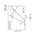
  • V GS _ a1 from the plotted V GS ⁇ I DS1 _ exclude _ RSD curve is taken as an example of deriving V GS _ ai from the plotted V GS ⁇ I DS1 _ exclude _ RSD as shown in FIG. 4 .
  • FIGS. 4 Referring to FIGS.
  • V G ⁇ I DS1 _ exclude _ RSD curve a series of V G 's are respectively applied to the gate of the MOS transistor while the substrate bias is fixed at V B1 , the corresponding series of V GS 's are calculated from the series of V G 's, the corresponding series of I DS1 's are measured, the corresponding series of I DS1 _ exclude _ RSD 'S are calculated by the equation of
  • I DS1 _ exclude _ RSD I DS ⁇ ⁇ 1 ⁇ V DS ( V DS - I DS ⁇ ⁇ 1 ⁇ R ⁇ ⁇ S ⁇ ⁇ D 1 , 2 )
  • I DS1 _ exclude _ RSD curve values are plotted with respect to the V GS .
  • the first-order differential of I DS1 _ exclude _ RSD with respect to V GS is plotted to determine the point of the curve with the maximal slope, a tangent line is plotted at the maximal-slope point of the curve, and the intercept of the tangent line with the x-axis is determined as V GS _ a1 .
  • V GS _ a2 can be derived from the V GS ⁇ I DS2 _ exclude _ RSD curve in a similar manner.
  • the above steps 36 , 38 and 40 are repeated until RSD 1,2 , V t1 _ 1,2 and V t2 _ 1,2 approach constant values without change after several times iterations.
  • ⁇ eff1 _ 1,2 and ⁇ eff2 _ 1,2 values can be calculated from the above derived RSD 1,2 V t1 _ 1,2 , and V t2 _ 1,2 values, by the equation of
  • FIG. 5 shows determination of the ⁇ k value that makes the set of RSD i,j values, ⁇ effp _ p,j values or V tq _ q,j values closest to each other in an example of this invention.
  • RSD 1,2 , RSD 1,3 RSD 2,3 , ⁇ eff1 _ 1,2 , ⁇ eff _ 1,3 , V t1 _ 1,2 and V t1 _ 1,3 were derived based on the method shown in FIGS. 3-4 .
  • the RSD value and the ⁇ eff value can be determined more accurately, and a more precise ⁇ value can be obtained as well.

Landscapes

  • Physics & Mathematics (AREA)
  • General Physics & Mathematics (AREA)
  • Engineering & Computer Science (AREA)
  • Microelectronics & Electronic Packaging (AREA)
  • Mathematical Physics (AREA)
  • Insulated Gate Type Field-Effect Transistor (AREA)
  • Mathematical Analysis (AREA)
  • Mathematical Optimization (AREA)
  • Computational Mathematics (AREA)
  • Pure & Applied Mathematics (AREA)
  • Data Mining & Analysis (AREA)
  • Theoretical Computer Science (AREA)
  • Operations Research (AREA)
  • Algebra (AREA)
  • Databases & Information Systems (AREA)
  • Software Systems (AREA)
  • General Engineering & Computer Science (AREA)

Abstract

A method for deriving characteristic values of a MOS transistor is described. A set of ηk values is provided. A set of VBi values (i=1 to M, M≧3) is provided. A set of RSDi,j (i=1 to M−1, j=i+1 to M) values each under a pair of VBi and VBj, or a set of Vtq _ q,j (q is one of 1 to M, j is 1 to M excluding q) values under VBq is derived for each ηk, with an iteration method. The ηk value making the set of RSDi,j values or Vtq _ q,j values closest to each other is determined as an accurate ηk value. The mean value of RSDi,j at the accurate ηk value is calculated as an accurate RSD value.

Description

BACKGROUND OF THE INVENTION
Field of Invention
This invention relates to a method for probing a MOS transistor, and particularly relates to a method for deriving characteristic values of a MOS transistor.
Description of Related Art
The sum (RSD) of the drain resistance RD and the source resistance RS and the effective carrier mobility μeff are important characteristic values for a MOS transistor. Recently, RSD extraction by using a single device is reported in two papers including Da-Wen Lin et al., IEEE Electron Device Letters, Vol. 28, No. 12, pp. 1132-1134, December 2007, and Da-Wen Lin et al., IEEE Transactions on Electron Devices, Vol. 57, No. 4, April 2010. The μeff value is directly calculated from the extracted RSD value. The single device of MOS transistor is illustrated in FIG. 1, together with the designation of certain parameters thereof that will be used hereafter.
The Vt values at different bias configurations and the empirical factor η (˜3 for PFET and ˜2 for NFET) are only inputs in the RSD equations in the above papers. However, if the values of Vt and η are not accurate, the extracted RSD and the μeff derived therefrom are not accurate either.
This invention gives a self-constant iteration method to find the accurate Vt and η so that determine the accurate RSD and μeff.
SUMMARY OF THE INVENTION
In view of the foregoing, this invention provides a method for deriving correct characteristic values of a MOS transistor.
In the method for deriving correct characteristic values of a MOS transistor, the MOS transistor comprises a substrate, a gate, a channel region, a source and a drain, the threshold voltage of the channel region is Vt, the voltage applied to the substrate is VB, the voltage applied to the gate is VG, the voltage across the source and the drain is VDS, the voltage across the gate and the source is VGS, a VGS making the MOS transistor operate in a constant-mobility region is VGS _ c, the current from the drain to the source is IDS, and the sum of the resistance RD of the drain and the resistance RS of the source is RSD. When a correct η value has been given, a correct RSD is derived by steps comprising the following steps a) to g). Step a) is applying different VB1 and VB2, respectively, to the substrate. Step b) is measuring IDS1 and IDS2 that correspond to VB1 and VB2, respectively. Step c) is giving respective initial values of Vt1 and Vt2, wherein Vt1 correspond to VB1 and Vt2 corresponds to VB2. Step d) is calculating RSD with the correct η value, Vt1 and Vt2 by the equation of
R S D = ( V GS_c + ( η - 1 ) V t 1 - η V t 2 - 0.5 V DS I DS 2 - V GS_c - V t 1 - 0.5 V DS I DS 1 ) × V DS η × ( V t 1 - V t 2 ) .
Step e) is plotting a VGS−IDS1 _ exclude _ RSD curve to derive VGS _ a1 and plotting a VGS−IDS2 _ exclude _ RSD curve to derive VGS _ a2, wherein IDS1 _ exclude _ RSD and IDS2 _ exclude _ RSD are calculated by the equations of
I DS 1 _exclude _RSD = I DS 1 × V DS ( V DS - I DS 1 × R S D ) and I DS 2 _exclude _RSD = I DS 2 × V DS ( V DS - I DS 2 × R S D ) ,
the VGS at the cross point on the VGS axis with a tangent line extrapolated from the point of the VGS−IDS1 _ exclude _ RSD curve where dIDS1 _ exclude _ RSD/dVGS is the maximal, and VGS _ a2 is the VGS at the cross point on the VGS axis with a tangent line extrapolated from the point of the VGS−IDS2 _ exclude _ RSD curve where dIDS2 _ exclude _ RSD/dVGS is maximal. Step f) is calculating new Vt1 and Vt2 by using the equations of Vt1=VGS _ a1−VDS/2 and Vt2=VGs _ a2−VDS/2. Step g) is repeating the above steps d), e) and f) until RSD, Vt1 and Vt2 approach constant values.
Because such obtained RSD, Vt1, and Vt2 are correct values, correct μeff1 and μeff2 values corresponding to VB1 and VB2 can then be calculated by using the correct RSD, Vt1, and Vt2:
μ eff 1 = L eff W eff C ox × I DS 1 ( V GS_c - V t 1 - V DS / 2 ) × ( V DS - R S D × I DS 1 ) u eff 2 = L eff W eff C ox × I DS 2 ( V GS_c - V t 2 - V DS / 2 ) × ( V DS - R S D × I DS 2 )
wherein Leff is the channel length, Weff is the channel width, and Cox is the inversion gate-oxide capacitance.
When the correct η value is unknown, the method for deriving characteristic values of a MOS transistor of this invention includes the following steps to derive the correct η value together with a correct RSD value. A set of ηk values (k=1 to N) is provided. A set of VBi values (i=1 to M, M≧3) is provided. For each ηk, a set of RSDi,j (i=1 to M−1, j=i+1 to M) values each under a pair of VBi and VBj, a set of μeffp _ p,j (p is one of 1 to M, j is 1 to M excluding p) values under a given VBp, and/or a set of Vtq _ q,j (q is one of 1 to M, j is 1 to M excluding q) values under a given VBq are derived by the iteration method described in the steps a) to g). Next, an accurate ηk value, which makes the set of RSDi,j values closest to each other, makes the set of μeffp _ p,j values closest to each other, and/or makes the set of Vtq _ q,j closest to each other, is determined. The mean value of RSDi,j is calculated as an accurate value for RSD.
With the method for deriving characteristic values of a MOS transistor of this invention, the RSD value can be determined more accurately by a more precise η value. Accurate η, RSD, μeff, and Vt could be obtained simultaneously and self-consistently.
In order to make the aforementioned and other objects, features and advantages of the present invention comprehensible, a preferred embodiment accompanied with figures is described in detail below.
BRIEF DESCRIPTION OF THE DRAWINGS
FIG. 1 illustrates a single device of MOS transistor whose characteristic values are to be investigated, together with the designation of certain parameters thereof.
FIG. 2 illustrates a method for deriving characteristic values of a MOS transistor according to an embodiment of this invention.
FIG. 3 illustrates the derivation of RSD1,2, Vt1 _ 1,2, Vt2 _ 1,2, μeff1 _ 1,2, and μeff2 _ 1,2 for each ηk value, as an example of the derivations of other RSDi,j, Vti _ i,j, Vtj _ i,j, μeff _ i,j, and μeff _ i,j, for the ηk value.
FIG. 4 illustrates the method of deriving VGS _ a1 by plotting a VGSDS1 _ exclude _ RSD curve, as an example of deriving VGS _ a1 (i=1, 2 . . . ).
FIG. 5 shows determination of the accurate ηk value that makes the set of RSDi,j values, μeffp _ p,j values or Vtq _ q _ j values closest to each other in an example of this invention.
DESCRIPTION OF EMBODIMENTS
It is noted that the following embodiments are intended to further explain this invention but not to limit the scope thereof. For example, though a correct η value is unknown and is to be determined in the illustrated embodiment, the method of this invention can also be applied to cases where a correct η value has been known.
FIG. 2 illustrates a method for deriving characteristic values of a MOS transistor according to an embodiment of this invention.
Referring to FIG. 2, in the step 20, a set of ηk values (k=1 to N) is provided. The set of ηk values are any non-identical positive real numbers larger than 1. In an exemplary embodiment, the ηk values are chosen as 1.1, 1.2, 1.3 . . . 3.9 and 4.0, but not limit thereto.
In next step 22 shown in FIG. 2, a set of VBi values (i=1 to M, M≧3) is provided. In an embodiment, M=3, and the different substrate biases VB1, VB2 and VB3 are, for example, 0 V, −0.5 V and −1V for NFET, and, 0 V, 0.5V, and 1V for PFET, respectively.
In next step 24, For each ηk, derive a set of RSDi,j (i=1 to M−1, j=i+1 to M) values each under a pair of VBi and VBj, a set of μeffp _ p,j (p is one of 1 to M, j is 1 to M excluding p) values under a given VBp, and/or a set of Vtq _ q,j (q is one of 1 to M, j is 1 to M excluding q) values under a given VBq corresponding to VBi and VBj by the iteration method of this invention that is exemplified later in FIG. 3.
In an embodiment of M=3 where three different substrate biases VB1, VB2 and VB3 are applied respectively, the set of RSDi,j values to be derived include: RSD1,2 derived from VB1 and VB2, RSD1,3 derived from VB1 and VB3, and RSD2,3 derived from VB2 and VB3.
In an embodiment of M=3 where three different substrate biases VB1, VB2 and VB3 are applied respectively and the μeff1 value under VB1 is investigated, the set of μeff1 _ 1,j values include: ηeff1 _ 1,2 derived from VB1 and VB2, and μeff1 _ 1,3 derived from VB1 and VB3.
In an embodiment of M=3 where three different substrate biases VB1, VB2 and VB3 are applied respectively and the Vt2 value under VB2 is investigated, the set of Vt2 _ 2,j values include: Vt2 _ 1,2 derived from VB1 and VB2, and Vt2 _ 2,3 derived from VB2 and VB3.
In next step 26, the accurate ηk value, which makes the set of RSDi,j values closest to each other, makes the μeff _ p, j values closest to each other, and/or makes the Vtq _ q,j values closest to each other, is determined.
In next step 28, the mean value of RSDi,j at the accurate ηk value is calculated as an accurate RSD, the mean value of μeffp _ p,j at the accurate ηk value is calculated as an accurate μeffp under the chosen VBp, and/or the mean value of Vtq _ q,j at the accurate ηk value is calculated as an accurate Vtq under the chosen VBq.
The iterative derivation of RSDi,j, Vti _ i,j, Vtj _ i,j, μeffi _ i,j, and μeffj _ i,j for each ηk can be exemplified by the iterative derivation of RSD1,2, Vt1 _ 1,2, Vt2 _ 1,2, μeff1 _ 1,2, and μeff2 _ 1,2 for a given ηk value as illustrated in FIG. 3.
Referring to FIG. 3, in step 30, the different VB1 and VB2 are respectively applied to the substrate, with the other voltages shown in FIG. 1 unchanged. In next step 32, the transistor current IDS1 and IDS2 that correspond to VB1 and VB2, respectively, are measured. In next step 34, respective initial values of Vt1 and Vt2 are given, wherein Vt1 correspond to VB1, and Vt2 corresponds to VB2. VGS _ c is a given VGS making the MOS transistor operate in a constant-mobility region, and the range of VGS corresponding to the constant-mobility region is determined by the well-known method described in the papers mentioned in [0002].
In next step 36, RSD is calculated with the ηk value, Vt1 _ 1,2 and Vt2 _ 1,2 by the equation of
R S D 1 , 2 = ( V GS_c + ( η k - 1 ) V t 1 _ 1 , 2 - η k V t 2 _ 1 , 2 - 0.5 V DS I DS 2 - V GS_c - V t 1 _ 1 , 2 - 0.5 V DS I DS 1 ) × V DS η k × ( V t 1 _ 1 , 2 - V t 2 _ 1 , 2 )
In next step 38, a VGS−IDS1 _ exclude _ RSD curve is plotted to derive VGS _ a1, and a VGS−IDS2 _ exclude _ RSD curve is plotted to derive VGS _ a2, wherein IDS1 _ exclude _ RSD and IDS2 _ exclude _ RSD are calculated by the equations of
I DS 1 _exclude _RSD = I DS 1 × V DS ( V DS - I DS 1 × R S D 1 , 2 ) and I DS 2 _exclude _RSD = I DS 2 × V DS ( V DS - I DS 2 × R S D 1 , 2 ) ,
is the VGS at the cross point on the VGS axis with a tangent line extrapolated from the point of the VGS−IDS1 _ exclude _ RSD curve where dIDS1 _ exclude _ RSD/dVGS is maximal, and VGS _ a2 is the VGS at the cross point on the VGS axis with a tangent line extrapolated from the point of the VGS−IDS2 _ exclude _ RSD curve where dIDS2 _ exclude _ RSD dVGS is maximal.
The method of deriving VGS _ a1 from the plotted VGS−IDS1 _ exclude _ RSD curve is taken as an example of deriving VGS _ ai from the plotted VGS−IDS1 _ exclude _ RSD as shown in FIG. 4. Referring to FIGS. 1 and 4, to plot the VGS−IDS1 _ exclude _ RSD curve, a series of VG's are respectively applied to the gate of the MOS transistor while the substrate bias is fixed at VB1, the corresponding series of VGS's are calculated from the series of VG's, the corresponding series of IDS1's are measured, the corresponding series of IDS1 _ exclude _ RSD'S are calculated by the equation of
I DS 1 _exclude _RSD = I DS 1 × V DS ( V DS - I DS 1 × R S D 1 , 2 ) ,
and the IDS1 _ exclude _ RSD curve values are plotted with respect to the VGS. The first-order differential of IDS1 _ exclude _ RSD with respect to VGS is plotted to determine the point of the curve with the maximal slope, a tangent line is plotted at the maximal-slope point of the curve, and the intercept of the tangent line with the x-axis is determined as VGS _ a1. VGS _ a2 can be derived from the VGS−IDS2 _ exclude _ RSD curve in a similar manner.
In next step 40, Vt1 _ 1,2 is calculated with VGS _ a1 and Vt2 _ 1,2 is calculated with VGS _ a2, by the equations of and Vt1 _ 1,2=VGS _ a1−VDS/2 and Vt2 _ 1,2=VGS _ a2−VDS/2. The above steps 36, 38 and 40 are repeated until RSD1,2, Vt1 _ 1,2 and Vt2 _ 1,2 approach constant values without change after several times iterations.
In step 42, μeff1 _ 1,2 and μeff2 _ 1,2 values can be calculated from the above derived RSD1,2 Vt1 _ 1,2, and Vt2 _ 1,2 values, by the equation of
μ eff 1 _ 1 , 2 = L eff W eff C ox × I DS 1 ( V GS_c - V t 1 _ 1 , 2 - V DS / 2 ) × ( V DS - R S D 1 , 2 × I DS 1 ) , μ eff 2 _ 1 , 2 = L eff W eff C ox × I DS 2 ( V GS_c - V t 2 _ 1 , 2 - V DS / 2 ) × ( V DS - R S D 1 , 2 × I DS 2 )
wherein Leff is the channel length, Weff is the channel width, and Cox is the inversion gate-oxide capacitance.
FIG. 5 shows determination of the ηk value that makes the set of RSDi,j values, μeffp _ p,j values or Vtq _ q,j values closest to each other in an example of this invention. In the example, the set of ηk values used were 1.1, 1.2, 1.3 . . . 3.9 and 4.0 (N=30), and three different biases (M=3), VB1=0 V, VB2=−0.5 V and VB3=−1V, were applied to the substrate of an NFET, respectively. For each ηk value, RSD1,2, RSD1,3 RSD2,3, μeff1 _ 1,2, μeff _ 1,3, Vt1 _ 1,2 and Vt1 _ 1,3 were derived based on the method shown in FIGS. 3-4.
Referring to FIG. 5, for each ηk value, how the set of RSD1,2, RSD1,3 and RSD2,3, the set of μeff1 _ 1,2 and μeff _ 1,3, or the set of Vt1 _ 1,2 and Vt1 _ 1,3 are close to each other was determined by the ratio of the difference between the maximal value and the minimal value in the set of values to the average of the set of values. Because “3.1” was the η value that made the set of RSD, μeff1 or Vt1 values closest to each other, it was the accurate η value, and the corresponding RSD, μeff1, or Vt1 calculated as the mean value of RSD1,2, RSD1,3 and RSD2,3, the mean value of μeff1 _ 1,2 and μeff _ 1,3, or the mean value of Vt1 _ 1,2 and Vt1 _ 1,3 was also the accurate value.
With the method for deriving characteristic values of a MOS transistor of this invention, the RSD value and the μeff value can be determined more accurately, and a more precise η value can be obtained as well.
This invention has been disclosed above in the preferred embodiments, but is not limited to those. It is known to persons skilled in the art that some modifications and innovations may be made without departing from the spirit and scope of this invention. Hence, the scope of this invention should be defined by the following claims.

Claims (10)

What is claimed is:
1. A method for deriving characteristic values of a MOS transistor, wherein the MOS transistor comprises a substrate, a gate, a channel region, a source and a drain, a threshold voltage of the channel region is Vt, a voltage applied to the substrate is VB, a voltage applied to the gate is VG, a voltage across the source and the drain is VDS, a voltage across the gate and the source is VGS, a VGS making the MOS transistor operate in a constant-mobility region is VGS _ c, a current from the drain to the source is IDS, and a sum of a resistance RD of the drain and a resistance RS of the source is RSD, the method comprising:
a) applying different VB1 and VB2, respectively, to the substrate;
b) measuring IDS1 and IDS2 that correspond to VB1 and VB2, respectively;
c) giving respective initial values of Vt1 and Vt2, wherein Vt1 corresponds to VB1 and Vt2 corresponds to VB2;
d) calculating RSD with a given η value, Vt1 and Vt2 by an equation of
R S D = ( V GS_c + ( η - 1 ) V t 1 - η V t 2 - 0.5 V DS I DS 2 - V GS_c - V t 1 - 0.5 V DS I DS 1 ) × V DS η × ( V t 1 - V t 2 ) ;
e) applying a series of VG's respectively to the gate while the voltage applied to the substrate is fixed at VB1, calculating a corresponding series of VGS's from the series of VG's and measuring a corresponding series of IDS1's to plot a plot of VGS vs. IDS1 _ exclude _ RSD to derive VGS _ a1, and applying a series of VG's respectively to the gate while the voltage applied to the substrate is fixed at VB2, calculating a corresponding series of VGS's from the series of VG's and measuring a corresponding series of IDS2's to plot a plot of VGS vs. IDS2 _ exclude _ RSD to derive VGS _ a2, wherein IDS1 _ exclude _ RSD and IDS2 _ exclude _ RSD are calculated by equations of
I DS 1 _exclude _RSD = I DS 1 × V DS ( V DS - I DS 1 × R S D ) and I DS 2 _exclude _RSD = I DS 2 × V DS ( V DS - I DS 2 × R S D ) ,
VGS _ a1 is the VGS at a cross point on the VGS axis with a tangent line extrapolated from a point of the VGS−IDS1 _ exclude _ RSD curve where dIDS1 _ exclude _ RSD/dVGS is maximal, and VGS _ a2 is the VGS at a cross point on the VGS axis with a tangent line extrapolated from a point of the VGS−IDS2 _ exclude _ RSD curve where dIDS2 _ exclude _ RSD/dVGS is maximal;
f) calculating Vt1 with VGS _ a1, and calculating Vt2 with VGS _ a2, by equations of
V t 1 = V GS_a 1 - V DS 2 and V t 2 = V GS_a 2 - V DS 2 ;
and
g) repeating the steps d), e) and f) several times until RSD, Vt1 and Vt2 approach constant values without change.
2. The method of claim 1, further comprising deriving effective carrier mobility μeff1 and μeff2 under VB1 and VB2, respectively, by equations of
μ eff 1 = L eff W eff C ox × I DS 1 ( V GS_c - V t 1 - V DS / 2 ) × ( V DS - R S D × I DS 1 ) μ eff 2 = L eff W eff C ox × I DS 2 ( V GS_c - V t 2 - V DS / 2 ) × ( V DS - R S D × I DS 2 ) ,
wherein Leff is a channel length, Weff is a channel width, and Cox is an inversion gate-oxide capacitance.
3. A method for deriving characteristic values of a MOS transistor, wherein the MOS transistor comprises a substrate, a gate, a channel region, a source and a drain, a threshold voltage of the channel region is Vt, a voltage applied to the substrate is VB, a voltage applied to the gate is VG, a voltage across the source and the drain is VDS, a voltage across the gate and the source is VGS, a VGS making the MOS transistor operate in a constant-mobility region is VGS _ c, a current from the drain to the source is IDS, and a sum of a resistance RD of the drain and a resistance RS of the source is RSD, the method comprising:
providing a set of ηk values (k=1 to N);
providing a set of VBi values (i=1 to M, M≧3);
for each ηk, derive a set of RSDi,j (i=1 to M−1, j=i+1 to M) values each under a pair of VBi and VBj, a set of μeffp _ p,j (p is one of 1 to M, j is 1 to M excluding p) values each under a VBp, and/or a set of Vtq _ q,j (q is one of 1 to M, j is 1 to M excluding q) values each under a VBq by the method of claim 2;
determine an accurate ηk value that makes the set of RSDi,j values closest to each other, makes the set of μeffp _ p,j values closest to each other, and/or makes the set of Vtq _ q,j values closest to each other; and
calculating a mean value of RSDi,j at the accurate ηk value as an accurate value of RSD.
4. The method of claim 3, wherein how the set of RSDi,j values, μeffp _ p,j values or Vtq _ q,j values are close to each other is determined by a ratio of a difference between a maximal value and a minimal value in the set of values to an average of the set of values.
5. The method of claim 3, further comprising:
calculating a mean value of μeffp _ p,j at the accurate ηk value as an accurate value of μeffp under VBp; and/or
calculating a mean value of Vtq _ q,j at the accurate ηk value as an accurate value of Vtq under VBq.
6. The method of claim 3, wherein M is equal to 3, and three different biases VB1, VB2 and VB3 are respectively applied to the substrate.
7. A method for deriving characteristic values of a MOS transistor, wherein the MOS transistor comprises a substrate, a gate, a channel region, a source and a drain, a threshold voltage of the channel region is Vt, a voltage applied to the substrate is VB, a voltage applied to the gate is VG, a voltage across the source and the drain is VDS, a voltage across the gate and the source is VGS, a VGS making the MOS transistor operate in a constant-mobility region is VGS _ c, a current from the drain to the source is IDS, and a sum of a resistance RD of the drain and a resistance RS of the source is RSD, the method comprising:
providing a set of ηk values (k=1 to N);
providing a set of VBi values (i=1 to M, M≧3);
for each ηk, derive a set of RSDi,j (i=1 to M−1, j=i+1 to M) values each under a pair of VBi and VBj, and/or a set of Vtq _ q,j (q is one of 1 to M, j is 1 to M excluding q) values each under a VBq by the iteration method described in the steps a) to g) of claim 1;
determine an accurate ηk value that makes the set of RSDi,j values closest to each other, and/or makes the set of Vtq _ q,j values closest to each other; and
calculating a mean value of RSDi,j at the accurate ηk value as an accurate value of RSD.
8. The method of claim 7, wherein how the set of RSDi,j values or Vtq _ q,j values are close to each other is determined by a ratio of a difference between a maximal value and a minimal value in the set of values to an average of the set of values.
9. The method of claim 7, further comprising:
calculating a mean value of Vtq _ q,j at the accurate ηk value as an accurate value of Vtq under VBq.
10. The method of claim 7, wherein M is equal to 3, and three different biases VB1, VB2 and VB3 are respectively applied to the substrate.
US13/894,021 2013-05-14 2013-05-14 Method for deriving characteristic values of MOS transistor Active 2036-02-25 US9632115B2 (en)

Priority Applications (1)

Application Number Priority Date Filing Date Title
US13/894,021 US9632115B2 (en) 2013-05-14 2013-05-14 Method for deriving characteristic values of MOS transistor

Applications Claiming Priority (1)

Application Number Priority Date Filing Date Title
US13/894,021 US9632115B2 (en) 2013-05-14 2013-05-14 Method for deriving characteristic values of MOS transistor

Publications (2)

Publication Number Publication Date
US20140343880A1 US20140343880A1 (en) 2014-11-20
US9632115B2 true US9632115B2 (en) 2017-04-25

Family

ID=51896444

Family Applications (1)

Application Number Title Priority Date Filing Date
US13/894,021 Active 2036-02-25 US9632115B2 (en) 2013-05-14 2013-05-14 Method for deriving characteristic values of MOS transistor

Country Status (1)

Country Link
US (1) US9632115B2 (en)

Families Citing this family (1)

* Cited by examiner, † Cited by third party
Publication number Priority date Publication date Assignee Title
US10627442B2 (en) * 2017-12-07 2020-04-21 Nanya Technology Corporation Method for estimating resistances of a source contact and a drain contact of a MOS transistor

Non-Patent Citations (6)

* Cited by examiner, † Cited by third party
Title
Baek et al., "Characteristics of the Series Resistance Extracted From Si Nanowire FETs Using the Y-Function Technique", 2010, IEEE Transactions on Nanotechnology, vol. 9, No. 2, Mar. 2010 pp. 212-217. *
Fleury et al., "A New Technique to Extract the Source/Drain Series Resistance of MOSFETs", 2009 IEEE Electron Device Letters, vol. 30, No. 9, Sep. 2009, pp. 975-977. *
J. J. Liou et al., "Extraction of the source and drain series resistances of MOSFETs" 1998, Chapter 5 of "Analysis and Design of MOSFETs" Kluwer Academic Publishers 1998 pp. *
Kim et al., "Accurate Extraction of Effective Channel Length and Source/Drain Series Resistance in Ultrashort-Channel MOSFETs by Iteration Method," IEEE Transactions on Electron Devices 55(10), Oct. 2008, pp. 2779-2784.
Lin et al., "A Constant-Mobility Method to Enable MOSFET Series-Resistance Extraction," IEEE Electron Device Letters 28(12), Dec. 2007, pp. 1132-1134.
Lin et al., "A Novel Method of MOSFET Series Resistance Extraction Featuring Constant Mobility Criteria and Mobility Universality," IEEE Transactions on Electron Devices 57(4), Apr. 2010, pp. 890-897.

Also Published As

Publication number Publication date
US20140343880A1 (en) 2014-11-20

Similar Documents

Publication Publication Date Title
CN104899350B (en) The modeling method of SiC MOSFET simulation models
TWI573007B (en) Constant current circuit and reference voltage circuit
JP4448533B2 (en) Semiconductor element parameter extraction method
CN101114314A (en) Simulation apparatus and simulation method, and semiconductor device fabrication method
US20190179991A1 (en) Method and system for testing optimization and molding optimization of semiconductor devices
CN105138803A (en) Universal mismatch model with consideration of temperature effect and method for extracting mismatch model
CN107944088A (en) A kind of constant mobility method of source/drain dead resistance in extraction nano-scaled MOSFET
CN107609269A (en) A kind of transistor noise model method for building up with biasing scaling
CN111368490A (en) Circuit model of transverse double-diffusion transistor and modeling method thereof
CN105302943A (en) Bias voltage dominant relevance mismatch model and extracting method
KR100938675B1 (en) Apparatus and Method for modeling of source-drain current of Thin Film Transistor
US20050086033A1 (en) Extracting semiconductor device model parameters
US9632115B2 (en) Method for deriving characteristic values of MOS transistor
CN105226054A (en) A kind of general mismatch model and extracting method thereof
GB2351156A (en) Modelling electrical characteristics of thin film transistors
Jandhyala et al. Inclusion of body doping in compact models for fully-depleted common double gate MOSFET adapted to gate-oxide thickness asymmetry
KR101363259B1 (en) Apparatus for extracting resistance, method for extracting resistance and computer-readable recording medium
US20110238393A1 (en) Spice model parameter output apparatus and method, and recording medium
JPH07176740A (en) Device model of mosfet and parameter extraction method
US11366946B2 (en) Method and apparatus for obtaining surface potential
Pourgholam et al. Modelling of drain current of MOSFET transistor in terms of gate oxide thickness
Henry et al. New access resistance extraction methodology for 14nm FD-SOI technology
Garcia-Sanchez et al. Extraction of MOSFET model parameters from the measured source-to-drain resistance
US6548420B2 (en) Measurement and analysis of mercury-based pseudo-field effect transistors
JP2007005416A (en) Method for extracting parameters of bsim model

Legal Events

Date Code Title Description
AS Assignment

Owner name: UNITED MICROELECTRONICS CORP., TAIWAN

Free format text: ASSIGNMENT OF ASSIGNORS INTEREST;ASSIGNORS:WU, YI-TING;HUANG, CHENG-TUNG;LEE, TSUNG-HAN;AND OTHERS;SIGNING DATES FROM 20130219 TO 20130508;REEL/FRAME:030407/0105

STCF Information on status: patent grant

Free format text: PATENTED CASE

MAFP Maintenance fee payment

Free format text: PAYMENT OF MAINTENANCE FEE, 4TH YEAR, LARGE ENTITY (ORIGINAL EVENT CODE: M1551); ENTITY STATUS OF PATENT OWNER: LARGE ENTITY

Year of fee payment: 4

MAFP Maintenance fee payment

Free format text: PAYMENT OF MAINTENANCE FEE, 8TH YEAR, LARGE ENTITY (ORIGINAL EVENT CODE: M1552); ENTITY STATUS OF PATENT OWNER: LARGE ENTITY

Year of fee payment: 8