US9628057B2 - Spread-spectrum clock generation circuit, integrated circuit and apparatus therefor - Google Patents
Spread-spectrum clock generation circuit, integrated circuit and apparatus therefor Download PDFInfo
- Publication number
- US9628057B2 US9628057B2 US14/909,212 US201314909212A US9628057B2 US 9628057 B2 US9628057 B2 US 9628057B2 US 201314909212 A US201314909212 A US 201314909212A US 9628057 B2 US9628057 B2 US 9628057B2
- Authority
- US
- United States
- Prior art keywords
- charge storage
- spread
- clock generation
- generation circuit
- spectrum clock
- Prior art date
- Legal status (The legal status is an assumption and is not a legal conclusion. Google has not performed a legal analysis and makes no representation as to the accuracy of the status listed.)
- Active
Links
Images


Classifications
-
- H—ELECTRICITY
- H03—ELECTRONIC CIRCUITRY
- H03K—PULSE TECHNIQUE
- H03K5/00—Manipulating of pulses not covered by one of the other main groups of this subclass
- H03K5/00006—Changing the frequency
-
- H—ELECTRICITY
- H03—ELECTRONIC CIRCUITRY
- H03K—PULSE TECHNIQUE
- H03K25/00—Pulse counters with step-by-step integration and static storage; Analogous frequency dividers
- H03K25/02—Pulse counters with step-by-step integration and static storage; Analogous frequency dividers comprising charge storage, e.g. capacitor without polarisation hysteresis
-
- H—ELECTRICITY
- H03—ELECTRONIC CIRCUITRY
- H03K—PULSE TECHNIQUE
- H03K3/00—Circuits for generating electric pulses; Monostable, bistable or multistable circuits
- H03K3/02—Generators characterised by the type of circuit or by the means used for producing pulses
- H03K3/023—Generators characterised by the type of circuit or by the means used for producing pulses by the use of differential amplifiers or comparators, with internal or external positive feedback
- H03K3/0231—Astable circuits
-
- H—ELECTRICITY
- H03—ELECTRONIC CIRCUITRY
- H03J—TUNING RESONANT CIRCUITS; SELECTING RESONANT CIRCUITS
- H03J2200/00—Indexing scheme relating to tuning resonant circuits and selecting resonant circuits
- H03J2200/10—Tuning of a resonator by means of digitally controlled capacitor bank
Definitions
- the field of this invention relates to a spread-spectrum clock generation circuit, integrated circuit and an apparatus, such as a clock system, therefor, and in particular to a circuit for varying an oscillation frequency of a switched current oscillator of a switched-mode power supply unit.
- Synchronous systems and circuits for example switch-mode power supplies (SMPS), microcontrollers, integrated digital/logic cores, etc. are often causing an undesired electromagnetic interference (EMI).
- SMPS switch-mode power supplies
- EMI undesired electromagnetic interference
- Such systems and circuits are driven by a clock signal, which due to its periodic nature, creates an unavoidably narrow frequency spectrum and radiate electromagnetic energy across a number of narrow bands spread around the clock frequency as well as the clock frequency harmonics. This results in a frequency spectrum that, at certain frequencies, may exceed the regulatory limits for electromagnetic interference set, for example, by EMI standards e.g. CISPR-25, IEC 61967.
- SSCG Spread-Spectrum Clock Generation
- the clock frequency is modulated such that the same energy is spread out over a wider bandwidth, which prevents systems from placing enough energy into any one narrowband to exceed the statutory limits.
- SSCG may also help attenuate EMI generated in successive clock harmonics.
- oscillators there are a number of different types of oscillators that can be used in clocked systems.
- One such oscillator type referred to as a switched current oscillator, is based on a capacitance charge/discharge process.
- frequency modulation via SSCG
- frequency modulation is achieved by varying capacitance, current or voltage (supply voltage or switching threshold) at a speed that is similar to an oscillation frequency of the oscillator.
- modulation is performed by periodic signals (that are not perfect due to low frequency tones appearing causing EMI) or by pseudo-random signals generated by programmable pseudo-random number generators (PPRNG).
- FIG. 1 illustrates a typical oscillator circuit for clock frequency spreading.
- Oscillator circuit 100 comprises current source 110 , variable capacitor 120 , PPRNG 130 , FET 140 differential (input) comparator 150 , flip-flop 160 and positive feedback capacitor C 1 .
- the differential comparator 150 compares sensed voltage 105 with reference voltage VREF. Oscillation happens by charging variable capacitance 120 by current source 110 until a voltage at node 105 reaches reference voltage VREF. Then comparator 150 switches and discharges variable capacitance 120 by FET 140 . The voltage on node 105 then drops to zero and the comparator switches again, and so forth.
- FET 140 must discharge variable capacitor 130 quickly, as otherwise it affects the accuracy of the oscillator circuit 100 .
- flip flop 160 is required to provide a 50% duty cycle as only a single current source is utilised.
- current source 110 and FET 140 may be implemented as two current sources, each with a series switch (e.g. a FET) controlled in opposite phases by comparator 150 .
- a small capacitor (C 1 ) is utilised to aid the differential comparator 150 in order to fully trip and to generate an appropriately shaped pulse.
- Frequency modulation (through SSCG) is performed by varying the capacitance value provided by the variable capacitor 120 , which is controlled by Programmable Pseudo-Random-Number Generator (PPRNG) 130 via a control signal (SYNC).
- the control signal is normally derived from an output of the oscillation circuit 100 .
- a multiple-bit leap-forward linear feedback shift register (LFSR) is widely used for generation of pseudo random (for example in a PPRNG) or true random numbers in communication and encryption.
- variable capacitor 120 is problematic.
- the overall capacitance of variable capacitor 120 needs to be relatively small for typically required oscillation frequencies.
- a desire to provide ‘uniform’ clock frequency spreading by SSCG often requires a higher resolution of PPRNG (i.e. a relatively large number of bits being used).
- PPRNG i.e. a relatively large number of bits being used.
- This requirement together with the fact that a minimum reproducible value of unit capacitance is limited in integrated technologies, leads to a need to have a larger overall capacitance value for variable capacitor 120 .
- this trade-off typically leads to increased cost and/or to increased power consumption in SSCG implementations.
- the resolution of a PPRNG and the possible clock spreading frequency bandwidth are closely inter-related, and it is therefore very difficult to modify either without affecting the other.
- SSCG may also be implemented by modulation of a current (e.g. current source 110 ) or of a voltage (e.g. VREF modulation).
- a current e.g. current source 110
- a voltage e.g. VREF modulation
- Such implementations require current or voltage output, digital-to-analog converter (DAC) usage together with a PPRNG. This again leads to cost and/or to consumption increase.
- DAC digital-to-analog converter
- the present invention provides a spread-spectrum clock generation circuit, an integrated circuit and an apparatus such as a switched-mode power supply unit comprising a spread-spectrum clock generation circuit, as described in the accompanying claims.
- FIG. 1 schematically shows a known oscillator circuit for clock frequency spreading.
- FIG. 2 schematically shows an example of an oscillator circuit for spread spectrum clock generation.
- FIG. 3 schematically shows a further example of an oscillator circuit for spread spectrum clock generation.
- FIG. 5 illustrates a simplified example block diagram of a switched-mode power supply unit.
- the present invention will now be described with reference to an example spread spectrum clock generation oscillator circuit, an integrated circuit comprising an oscillator circuit and an apparatus, such as say, a switched-mode power supply unit or a synchronous digital system (such as integrated microcontrollers, digital/logic cores), and adapted in accordance with some embodiments of the present invention.
- a switched-mode power supply unit or a synchronous digital system such as integrated microcontrollers, digital/logic cores
- inventive concept described herein is not limited to specific features of the illustrated example, and may equally be implemented within alternative communication units, integrated circuits and applications.
- a spread spectrum generation circuit and an apparatus such as a switched mode power supply is described that has a defined clock spreading frequency bandwidth that may not depend on the PPRNG resolution (number of bits).
- FIG. 2 schematically shows an example of an oscillator circuit 200 used as a core of spread spectrum clock generation.
- oscillator circuit 200 may comprise a switched current network 202 , operably coupled to a comparison element 206 via a shunt charge storage device 204 .
- the example oscillator circuit 200 comprises a, comparison element 206 and charge storage arrangement 208 .
- additional circuitry may be utilized to compensate temperature, supply or process dependence.
- switched current network 202 may comprise more than one current source 203 . Further, switched current network 202 may be switched via at least one switching device 205 . In this example, an array of two switching devices 205 is utilised. In other examples, a plurality of switching devices may be used. In some examples, the at least one switching device 205 may be one of a type of field effect transistor (FET), junction field effect transistor (JFET) metal oxide semiconductor field effect transistor (MOSFET), bipolar junction transistor (BJT), or the like. Further, the at least one switching device 205 may be formed of traditional materials, such as amorphous silicon, polycrystalline silicon and organic materials.
- FET field effect transistor
- JFET junction field effect transistor
- MOSFET metal oxide semiconductor field effect transistor
- BJT bipolar junction transistor
- the at least one switching device 205 may be formed of traditional materials, such as amorphous silicon, polycrystalline silicon and organic materials.
- the at least one switching device 205 may be formed utilising materials such as carbon, in the form of carbon nanotubes or graphene, for example.
- switching devices 205 may utilise the same type of device. In other examples, different devices may be utilised for each switching device 205 .
- switched current network 202 may be operably coupled between a supply voltage VDD and a ground terminal.
- the shunt charge storage device 204 may comprise a capacitor, for example an electrolytic, polymer or solid dielectric type capacitor.
- shunt charge storage device 204 may be utilised to limit a voltage applied to an input of comparison element 206 .
- the charge storage device may comprise a series of charge storage devices.
- the charge storage device 204 may be operably coupled to comparison element 206 .
- comparison element 206 may comprise a single threshold comparator. In other examples, comparison element 206 may comprise a differential type comparator. Further, comparison element 206 may be formed of a series of logic gates, for example inverters. In some examples, comparison element 206 may be formed of at least two inverter logic gates, thereby approximating a single threshold comparative element. In other examples, a plurality of logic gates may be utilised to approximate the function of a single threshold comparative element. In some examples, comparative element 206 may be operably coupled to a voltage supply VDD.
- oscillator circuit 200 may utilise the same voltage source. In other examples, different voltage sources may be utilised for different parts of the oscillator circuit 200 .
- a charge storage arrangement (which is some examples is a charge storage circuit) 208 may be operably coupled at the input and output of comparison element 206 .
- the charge storage arrangement 208 may comprise a (positive) feedback capacitor to set a first oscillation frequency, and a parallel switched charge storage arrangement to set a second oscillation frequency.
- parallel switched charge storage arrangement may comprise an array of charge storage elements.
- the charge storage arrangement 208 is operably coupled in a feedback arrangement, whereby a capacitive value of the charge storage device (e.g. positive feedback capacitor) sets/affects a frequency modulation/frequency spreading/dithering of the oscillation frequency of oscillator circuit 200 .
- the input ‘A’ represents a capacitance that is a sum of the capacitance value of shunt charge storage device 204 and charge storage arrangement 208 . If we assume that an initial voltage ‘A’ on the input of the comparator 206 is above a threshold voltage V TH of the comparator 206 and the input ‘A’ is discharged by the discharging branch of the switched current network 202 to the threshold voltage of the comparator, the potential at the input ‘A’ will be gradually decreased.
- the output ‘B’ of the comparator 206 switches to another state, which causes an abrupt drop of the potential of input ‘A’ due to charge storage arrangement 208 , thereby causing a charging current to flow into the input ‘A’ of the comparator from the charge branch of the switched current network 202 . This, in turn, causes the potential at the input ‘A’ to gradually increase.
- a value of abruptly drop/rise voltage on the input of the comparator is defined by an output voltage swing on the output ‘B’ of the comparator 206 , which is, for example, VDD and a division ratio of capacitive divider formed by shunt charge storage device 204 and charge storage arrangement 208 .
- Cf is a capacitance representing switched charge storage arrangement 208 .
- the oscillation frequency, f does not depend on the value of shunt charge storage device 204 (Ci) or on an exact value of the threshold (V TH ) of the comparison element 206 . Instead, the oscillation frequency, f, allows using a single input comparator that, in one simple implementation example, may be a chain of inverters.
- charge storage arrangement 208 may be implemented as a feedback capacitor (Cf) located in parallel to a switched capacitor arrangement, examples of which are illustrated further in FIG. 3 and FIG. 4 .
- the feedback capacitor (Cf) may comprise a plurality of feedback capacitors in order to create a desired Cf value.
- feedback capacitor (Cf) may comprise one or more additional charge storage element(s)/device(s).
- frequency modulation/spreading/dithering is performed by selectively applying (activating in the circuit) a number of simultaneously switched charge storage devices, for example capacitors that are located in parallel to feedback capacitor (Cf), as further described with respect to FIG. 3 and FIG. 4 .
- a ‘C-2C’ digital-to-analog (DAC) circuit/arrangement may be used to represent a number of simultaneously switched capacitors, to enable the clock-frequency spreading bandwidth to not be dependent upon a DAC's resolution, as further described with respect to FIG. 4 .
- a number of the simultaneously switched capacitors in parallel to a feedback capacitor (Cf) may be controlled by PPRNG, implemented as a linear feedback shift register (LFSR), which in some examples is used as a pseudo-noise sequence generator.
- PPRNG implemented as a linear feedback shift register (LFSR)
- FIG. 3 a schematic diagram illustrating a further example of an oscillator circuit for spread spectrum clock generation is shown.
- FIG. 3 comprises features already described with reference to FIG. 2 and, therefore, only new features are discussed in any detail.
- charge storage arrangement 208 may comprise a charge storage device, for example, feedback capacitor (Cf) 310 and a switched charge storage arrangement 312 .
- feedback capacitor (Cf) 310 may comprise a single charge storage device/element.
- feedback capacitor (Cf) 310 may comprise more than one charge storage device/element, forming an arrangement of charge storage devices/elements.
- switched charge storage arrangement 312 may comprise a plurality of charge storage elements 314 , 316 , 318 , 320 .
- charge storage elements 314 , 316 , 318 and 320 may all have the same capacitance value.
- the charge storage elements 314 , 316 , 318 and 320 may be binary weighted. In further examples, some or all of charge storage elements 314 , 316 , 318 and 320 may have different capacitances. In further examples, a number of the charge storage elements 314 , 316 , 318 and 320 may be different, i.e. more or less than the four elements shown in this example.
- feedback capacitor (Cf) 310 defines a first capacitance that is operable to set a first oscillation frequency of oscillator circuit 300 .
- switched charge storage arrangement 312 located in parallel to feedback capacitor (Cf) 310 , is arranged to define a second capacitance that is operable to set a second oscillation frequency of oscillator circuit 300 .
- switching module 322 may enable at least one charge storage element 314 , 316 , 318 and 320 of a plurality of selectable charge storage elements, located in parallel with feedback capacitor (Cf) 310 , to define the second oscillation frequency of oscillator circuit 300 .
- feedback capacitor (Cf) 310 may be disabled, and the second oscillation frequency may be set using solely one or more of selectable charge storage elements 314 , 316 , 318 , 320 . As one or more or each of charge storage elements 314 , 316 , 318 and 320 may be selectively enabled, they may also be selectively disabled, for example where only the first oscillation frequency defined by feedback capacitor (Cf) 310 is required.
- feedback capacitor (Cf) 310 may define a minimum capacitance, thereby providing a maximum oscillation frequency.
- switched charge storage arrangement 312 may define a capacitance that, when combined with feedback capacitor (Cf) 310 , provides a minimum oscillation frequency.
- switched charge storage arrangement 312 may provide a range of capacitance values between a maximum and a minimum value, wherein a minimum value may be set by the feedback capacitor (Cf) 310 alone with the maximum value being set by the total capacitance of switched charge storage arrangement 312 in parallel combination with the feedback capacitor (Cf) 310 .
- a range of available capacitance values may be set by enabling one or more charge storage elements 314 , 316 , 318 and 320 .
- charge storage arrangement 208 may dynamically alter the switching frequency of the oscillator circuit 300 , thereby allowing for spread spectrum clock generation.
- switching module 322 may switch charge storage elements 314 , 316 , 318 and 320 in a simultaneous fashion. In other examples, switching module 322 may switch charge storage elements 314 , 316 , 318 and 320 in an asynchronous fashion.
- the pseudo-random switching sequence may be advantageous in reducing periodic switching patterns within the switching sequence, thereby potentially reducing an appearance of low frequency signals within the spectrum.
- f OSC,MIN I /(2* VDD *( cf+ca )).
- f OSC,MIN I /(2* VDD *( cf+ca )
- ⁇ f OSC f OSC,MAX ⁇ f OSC,MIN
- switching module 322 may control a weighted capacitor array.
- the weighted capacitor array may comprise four charge storage devices 314 , 316 , 318 and 320 with respective unit capacitances ‘C’, ‘2C’, ‘4C’, ‘8C’.
- the total unit capacitance of the switched charge storage arrangement 312 may be defined by 2 N ⁇ 1, where ‘N’ is the number of bits of the switching module 322 .
- a total of ‘15C’ unit capacitances may be required to implement a 4-bit clock frequency spreading on sixteen different frequencies distributed over the desired band.
- a second oscillator range namely clock frequency spreading band
- switching module 322 may comprise a 10-bit LFSR for switching a switched charge storage arrangement 312 .
- charged storage arrangement 408 may comprise switching module 422 , feedback capacitor, Cf, 310 and switched charge storage arrangement 412 .
- switching module 422 may comprise a 4 bit linear feedback shift register (LFSR) that may comprise, in some examples, a series of flip flops 403 , 404 , 405 , 406 , 407 and one or more exclusive OR (XOR) gates 409 .
- LFSR linear feedback shift register
- switching module 422 may comprise any number of bits, which may be represented by flip flops, latches or any logic equivalent, for example.
- the switching module 422 may be operable to provide a pseudo-random switching sequence.
- switching module 422 may comprise a series of AND gates 411 , 413 , 415 and 417 (or types of logic gates, buffers or push-pull switches, etc.) to drive charged storage arrangement 408 .
- the output of a LFSR may be connected directly to switched change storage arrangement 412 .
- switched charge storage arrangement 412 may comprise a charged storage device C-2C ladder network.
- the oscillation frequency of the oscillator circuit 300 may be any value between the minimum and maximum oscillation frequency, or Ca may be made any value between ‘0’ and ‘2C’, by enabling one or more charge storage devices within switched charge storage arrangement 412 in a periodic or pseudo-random fashion.
- C-2C may provide the same advantages of an inexpensive and relatively easy to manufacture solution, since only 3*N ⁇ 1 unit capacitors are required. This is in contrast to weighted capacitor array that requires 2 N ⁇ 1 unit capacitors.
- an advantage of utilising a capacitive ladder network as a switched charge storage arrangement 412 may be that the minimum and maximum frequencies for spread spectrum clock generation are not dependent on the number of bits of the switching module 422 . Further, utilising a capacitive ladder network as switched charge storage arrangement 412 may allow for fewer devices to be utilised than currently utilised in the art for a given bit size of clock frequency spreading or switching module.
- C-2C ladders for DACs are rarely used in an integrated implementation due to the presence of an intrinsic parasitic capacitance associated with an integrated capacitance's bottom plate.
- the influence of parasitic capacitances thus appears as missing codes (gaps) in the transfer function of the DAC.
- the inventors have recognised that such a concern is not a problem when implemented for spread spectrum spreading/dithering.
- a C-2C ladder of switched charge storage elements 422 may be implemented with a different radix than ‘2’ (e.g. between ‘1’ and ‘2’, or more than ‘2’).
- a charge scaling DAC approach may be used, whereby the circuit appears as a superposition of a binary-weighted DAC together with a C-2C DAC.
- switching module 422 may be a 4-bit LFSR switching switched charge storage arrangement 412 , which in some examples may be a ladder network.
- the ladder network may comprise unit capacitance ‘C’ 419 operably coupled to a further unit capacitance ‘2C’ 421 for each logic gate 411 , 413 , 415 and wherein the n th logic gate, in this example logic gate 417 , may comprise unit capacitance ‘C’ 419 operably coupled to a grounded further unit capacitance ‘C’ 419 .
- the charge storage elements may all have varying values of unit capacitance.
- the charge storage elements may all have substantially the same value of unit capacitance.
- the charge storage elements may combine a ladder network with a weighted network.
- a weighted capacitor array designed for the same frequency spreading performance would utilise a total of ‘150C’+‘15C’ unit capacitances. Therefore, there is a significant decrease in the number of unit capacitances required if utilising a ladder network.
- switching module 422 may comprise a 10-bit LFSR switching a capacitive ladder network (as switched charge storage arrangement 412 ), which now requires ‘29C’ unit capacitance (e.g. 11*‘C’ unit capacitances and 9*‘2C’ unit capacitances) for C-2C ladder network (‘1023C’ for weighted capacitor array).
- ‘29C’ unit capacitance e.g. 11*‘C’ unit capacitances and 9*‘2C’ unit capacitances
- C-2C ladder network ‘1023C’ for weighted capacitor array
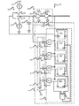
- FIG. 5 there is illustrated an example of a simplified block diagram of part of an electronic device 500 adapted in accordance with an example of the present invention.
- the illustrated example apparatus is a switched-mode power supply (SMPS) unit, such as a DC/DC converter.
- SMPS switched-mode power supply
- the concepts described herein may equally be applied to any system/component operable at a clock frequency defined by an internal or external oscillator circuit e.g. to microcontrollers, integrated digital/logic cores, etc.
- the electronic device 500 comprises an input energy source 502 operably coupled to input filter 504 and then coupled to one or more switch(es) 506 that is/are arranged to control energy transfer media 508 .
- switch(es) 506 may be at least one electrical device that can break an electrical circuit, interrupting the current or diverting it from one conductor to another, for example a type of relay, field effect transistor (FET, MOSFET, JFET), bipolar junction transistor (BJT), isolated gate bipolar transistor (IGBT) or different types of silicon controlled rectifier (SCR), etc.
- Energy transfer media 508 may be at least one electrical device that can store energy, for example an inductor or capacitor. Energy transfer media 508 is operably coupled to output filter 510 , which in turn is operably coupled to output (or load) 512 .
- the illustrated electronic device 500 further comprises negative feedback 514 that contains feedback circuit 516 , pulse wave modulated (PWM) control circuit 518 , voltage/current reference circuit 520 .
- the PWM control circuit 518 controls the one or more switch(es) 506 , which are switched with a fixed frequency that has a duty circle as a function of a difference between the signals provided by the feedback circuit 518 and voltage/current reference circuit 520 .
- the fixed frequency is provided by oscillator circuit 522 , which sets an operation/clock frequency of the whole system of SMPS.
- oscillator circuit 522 is a spread-spectrum clock generation oscillator circuit as previously described, which may negate or reduce any switching noise (and/or undesired electromagnetic interference (EMI) which may exceed the regulatory limits requested to SMPS) created by the one or more switch(es) 506 .
- EMI undesired electromagnetic interference
- connections as discussed herein may be any type of connection suitable to transfer signals from or to the respective nodes, units or devices, for example via intermediate devices. Accordingly, unless implied or stated otherwise, the connections may for example be direct connections or indirect connections.
- the connections may be illustrated or described in reference to being a single connection, a plurality of connections, unidirectional connections, or bidirectional connections. However, different embodiments may vary the implementation of the connections. For example, separate unidirectional connections may be used rather than bidirectional connections and vice versa.
- plurality of connections may be replaced with a single connection that transfers multiple signals serially or in a time multiplexed manner. Likewise, single connections carrying multiple signals may be separated out into various different connections carrying subsets of these signals. Therefore, many options exist for transferring signals.
- Each signal described herein may be designed as positive or negative logic.
- the signal In the case of a negative logic signal, the signal is active low where the logically true state corresponds to a logic level zero.
- the signal In the case of a positive logic signal, the signal is active high where the logically true state corresponds to a logic level one.
- any of the signals described herein can be designed as either negative or positive logic signals. Therefore, in alternate embodiments, those signals described as positive logic signals may be implemented as negative logic signals, and those signals described as negative logic signals may be implemented as positive logic signals.
- assert or ‘set’ and ‘negate’ (or ‘de-assert’ or ‘clear’) are used herein when referring to the rendering of a signal, status bit, or similar apparatus into its logically true or logically false state, respectively. If the logically true state is a logic level one, the logically false state is a logic level zero. And if the logically true state is a logic level zero, the logically false state is a logic level one.
- any arrangement of components to achieve the same functionality is effectively ‘associated’ such that the desired functionality is achieved.
- any two components herein combined to achieve a particular functionality can be seen as ‘associated with’ each other such that the desired functionality is achieved, irrespective of architectures or intermediary components.
- any two components so associated can also be viewed as being ‘operably connected’, or ‘operably coupled’, to each other to achieve the desired functionality.
- the illustrated examples may be implemented as circuitry located on a single integrated circuit or within a same device.
- the examples may be implemented as any number of separate integrated circuits or separate devices interconnected with each other in a suitable manner.
- the examples, or portions thereof may implemented as soft or code representations of physical circuitry or of logical representations convertible into physical circuitry, such as in a hardware description language of any appropriate type.
- the invention is not limited to physical devices or units implemented in non-programmable hardware but can also be applied in programmable devices or units able to perform the desired device functions by operating in accordance with suitable program code, such as mainframes, minicomputers, servers, workstations, personal computers, notepads, personal digital assistants, electronic games, automotive and other embedded systems, cell phones and various other wireless devices, commonly denoted in this application as ‘computer systems’.
- suitable program code such as mainframes, minicomputers, servers, workstations, personal computers, notepads, personal digital assistants, electronic games, automotive and other embedded systems, cell phones and various other wireless devices, commonly denoted in this application as ‘computer systems’.
- any reference signs placed between parentheses shall not be construed as limiting the claim.
- the word ‘comprising’ does not exclude the presence of other elements or steps then those listed in a claim.
- the terms ‘a’ or ‘an’, as used herein, are defined as one or more than one.
- the use of introductory phrases such as ‘at least one’ and ‘one or more’ in the claims should not be construed to imply that the introduction of another claim element by the indefinite articles ‘a’ or ‘an’ limits any particular claim containing such introduced claim element to inventions containing only one such element, even when the same claim includes the introductory phrases ‘one or more’ or ‘at least one’ and indefinite articles such as ‘a’ or ‘an’.
Landscapes
- Engineering & Computer Science (AREA)
- Power Engineering (AREA)
- Physics & Mathematics (AREA)
- Nonlinear Science (AREA)
- Semiconductor Integrated Circuits (AREA)
Abstract
Description
ΔV=VDD*Cf/(Ci+Cf) [1]
where:
T RISE =ΔV*(Ci+Cf)/I RISE =VDD*Cf/I RISE and T DROP =ΔV*(Ci+Cf)/I DROP =VDD*Cf/I DROP [2]
where IRISE and IDROP are the charge and discharge currents formed by switched
f=1/(T RISE +T DROP)=I/(2*VDD*Cf) [3]
f OSC,MAX =I/(2*VDD*Cf). [4]
f OSC,MIN =I/(2*VDD*(cf+ca)). [5]
Thus, the spectral band of clock frequency spreading may be defined as:
Δf OSC =f OSC,MAX −f OSC,MIN [6]
with a center frequency f OSC=(f OSC,MAX +f OSC,MIN)/2. [7]
where:
Δf OSC /f OSC=2*Ca/(2*Cf+Ca)=Ca/Cf. [8]
Claims (19)
Applications Claiming Priority (1)
| Application Number | Priority Date | Filing Date | Title |
|---|---|---|---|
| PCT/RU2013/000664 WO2015016734A1 (en) | 2013-08-01 | 2013-08-01 | Spread-spectrum clock generation circuit, integrated circuit and apparatus therefor |
Publications (2)
| Publication Number | Publication Date |
|---|---|
| US20160191029A1 US20160191029A1 (en) | 2016-06-30 |
| US9628057B2 true US9628057B2 (en) | 2017-04-18 |
Family
ID=50184978
Family Applications (1)
| Application Number | Title | Priority Date | Filing Date |
|---|---|---|---|
| US14/909,212 Active US9628057B2 (en) | 2013-08-01 | 2013-08-01 | Spread-spectrum clock generation circuit, integrated circuit and apparatus therefor |
Country Status (2)
| Country | Link |
|---|---|
| US (1) | US9628057B2 (en) |
| WO (1) | WO2015016734A1 (en) |
Cited By (5)
| Publication number | Priority date | Publication date | Assignee | Title |
|---|---|---|---|---|
| US20170034842A1 (en) * | 2014-05-14 | 2017-02-02 | Sony Corporation | Electronic device and wireless communication method in wireless communication system |
| US20190115986A1 (en) * | 2017-10-18 | 2019-04-18 | Texas Instruments Incorporated | SWITCH MODE DIRECT CURRENT-TO-DIRECT CURRENT (DC-to-DC) CONVERTERS WITH REDUCED SPURIOUS NOISE EMISSION |
| US10579833B1 (en) * | 2014-12-16 | 2020-03-03 | Thales Esecurity, Inc. | Tamper detection circuit assemblies and related manufacturing processes |
| US20200195253A1 (en) * | 2018-12-13 | 2020-06-18 | Stichting Imec Nederland | Frequency Sweep Generator and Method |
| US10789999B1 (en) * | 2019-09-06 | 2020-09-29 | Phison Electronics Corp. | Spread spectrum clock generator, memory storage device and signal generation method |
Families Citing this family (7)
| Publication number | Priority date | Publication date | Assignee | Title |
|---|---|---|---|---|
| JP6618730B2 (en) * | 2015-08-03 | 2019-12-11 | ローム株式会社 | Oscillator circuit |
| US10225082B2 (en) | 2016-07-26 | 2019-03-05 | International Business Machines Corporation | Carbon nanotube physical entropy source |
| JP6773902B2 (en) * | 2016-10-13 | 2020-10-21 | アナログ・ディヴァイシス・グローバル・アンリミテッド・カンパニー | Systems and methods for transmitting power across insulation barriers |
| US10491428B2 (en) | 2018-04-27 | 2019-11-26 | Hewlett Packard Enterprise Development Lp | Current supply for an opto-electronic device |
| US10484089B1 (en) * | 2018-04-27 | 2019-11-19 | Hewlett Packard Enterprise Development Lp | Driver assisted by charge sharing |
| US11258410B2 (en) * | 2018-08-03 | 2022-02-22 | University Of Utah Research Foundation | Apparatuses and methods for hybrid switched capacitor array power amplifiers |
| US12131245B2 (en) * | 2020-10-20 | 2024-10-29 | Intel Corporation | Bayesian neural network and methods and apparatus to operate the same |
Citations (9)
| Publication number | Priority date | Publication date | Assignee | Title |
|---|---|---|---|---|
| US4465983A (en) | 1982-09-27 | 1984-08-14 | Northern Telecom Limited | CMOS Oscillator having positive feedback capacitor charged and discharged with constant currents |
| GB2293289A (en) | 1994-06-06 | 1996-03-20 | Seiko Epson Corp | Controllable oscillator for a matrix display |
| US6326859B1 (en) * | 1999-07-01 | 2001-12-04 | Telefonaktiebolaget Lm Ericsson (Publ) | Oscillator circuit having trimmable capacitor array receiving a reference current |
| EP1592154A2 (en) | 2004-04-29 | 2005-11-02 | Linear Technology Corporation | Methods and circuits for frequency modulation that reduce the spectral noise of switching regulators |
| US6980039B1 (en) | 2004-03-03 | 2005-12-27 | Rf Micro Devices, Inc. | DC-DC converter with noise spreading to meet spectral mask requirements |
| US7098709B2 (en) | 2003-12-04 | 2006-08-29 | Fujitsu Limited | Spread-spectrum clock generator |
| US20080130712A1 (en) | 2006-10-30 | 2008-06-05 | Chaitanya Chava | Switched-current oscillator for clock-frequency spreading |
| US20090160503A1 (en) | 2007-12-24 | 2009-06-25 | Elite Semiconductor Memory Technology Inc. | Triangle wave generator and spread spectrum control circuit thereof |
| US7843278B2 (en) | 2008-06-06 | 2010-11-30 | Niko Semiconductor Co., Ltd. | Frequency jitter generation circuit |
-
2013
- 2013-08-01 WO PCT/RU2013/000664 patent/WO2015016734A1/en not_active Ceased
- 2013-08-01 US US14/909,212 patent/US9628057B2/en active Active
Patent Citations (10)
| Publication number | Priority date | Publication date | Assignee | Title |
|---|---|---|---|---|
| US4465983A (en) | 1982-09-27 | 1984-08-14 | Northern Telecom Limited | CMOS Oscillator having positive feedback capacitor charged and discharged with constant currents |
| GB2293289A (en) | 1994-06-06 | 1996-03-20 | Seiko Epson Corp | Controllable oscillator for a matrix display |
| US6075420A (en) | 1994-06-06 | 2000-06-13 | Seiko Epson Corporation | Oscillators with charging and discharging circuits |
| US6326859B1 (en) * | 1999-07-01 | 2001-12-04 | Telefonaktiebolaget Lm Ericsson (Publ) | Oscillator circuit having trimmable capacitor array receiving a reference current |
| US7098709B2 (en) | 2003-12-04 | 2006-08-29 | Fujitsu Limited | Spread-spectrum clock generator |
| US6980039B1 (en) | 2004-03-03 | 2005-12-27 | Rf Micro Devices, Inc. | DC-DC converter with noise spreading to meet spectral mask requirements |
| EP1592154A2 (en) | 2004-04-29 | 2005-11-02 | Linear Technology Corporation | Methods and circuits for frequency modulation that reduce the spectral noise of switching regulators |
| US20080130712A1 (en) | 2006-10-30 | 2008-06-05 | Chaitanya Chava | Switched-current oscillator for clock-frequency spreading |
| US20090160503A1 (en) | 2007-12-24 | 2009-06-25 | Elite Semiconductor Memory Technology Inc. | Triangle wave generator and spread spectrum control circuit thereof |
| US7843278B2 (en) | 2008-06-06 | 2010-11-30 | Niko Semiconductor Co., Ltd. | Frequency jitter generation circuit |
Non-Patent Citations (9)
Cited By (9)
| Publication number | Priority date | Publication date | Assignee | Title |
|---|---|---|---|---|
| US20170034842A1 (en) * | 2014-05-14 | 2017-02-02 | Sony Corporation | Electronic device and wireless communication method in wireless communication system |
| US10517108B2 (en) * | 2014-05-14 | 2019-12-24 | Sony Corporation | Electronic device and wireless communication method in wireless communication system |
| US10973036B2 (en) | 2014-05-14 | 2021-04-06 | Sony Corporation | Electronic device and wireless communication method in wireless communication system |
| US10579833B1 (en) * | 2014-12-16 | 2020-03-03 | Thales Esecurity, Inc. | Tamper detection circuit assemblies and related manufacturing processes |
| US11250171B1 (en) | 2014-12-16 | 2022-02-15 | Thales Esecurity, Inc. | Three-dimensional (3D) printing of a tamper sensor assembly |
| US20190115986A1 (en) * | 2017-10-18 | 2019-04-18 | Texas Instruments Incorporated | SWITCH MODE DIRECT CURRENT-TO-DIRECT CURRENT (DC-to-DC) CONVERTERS WITH REDUCED SPURIOUS NOISE EMISSION |
| US20200195253A1 (en) * | 2018-12-13 | 2020-06-18 | Stichting Imec Nederland | Frequency Sweep Generator and Method |
| US10938393B2 (en) * | 2018-12-13 | 2021-03-02 | Stichting Imec Nederland | Frequency sweep generator and method |
| US10789999B1 (en) * | 2019-09-06 | 2020-09-29 | Phison Electronics Corp. | Spread spectrum clock generator, memory storage device and signal generation method |
Also Published As
| Publication number | Publication date |
|---|---|
| US20160191029A1 (en) | 2016-06-30 |
| WO2015016734A1 (en) | 2015-02-05 |
Similar Documents
| Publication | Publication Date | Title |
|---|---|---|
| US9628057B2 (en) | Spread-spectrum clock generation circuit, integrated circuit and apparatus therefor | |
| CN101496280B (en) | Self-Calibrating Digital Pulse Width Modulator (DPWM) | |
| US7342528B2 (en) | Circuit and method for reducing electromagnetic interference | |
| CN102361396B (en) | Special pseudorandom sequence dither frequency control oscillator | |
| US10243553B2 (en) | System and method for a switch transistor driver | |
| US7504897B2 (en) | Switched-current oscillator for clock-frequency spreading | |
| US20100165675A1 (en) | System and method for controlling variations of switching frequency | |
| CN109863697B (en) | High Linearity Digital Time Converter for Low Noise All Digital Phase Locked Loop | |
| TWI403091B (en) | Onion waveform generator and spread spectrum clock generator using the same | |
| US20090128198A1 (en) | Digital frequency synthesizer | |
| JP2022534880A (en) | Multiple dithering profile signal generation | |
| CN100555872C (en) | Spread spectrum clock generation circuit and its control method | |
| US11601053B2 (en) | Spectral shaping of spread spectrum clocks/frequencies through post processing | |
| EP2584719B1 (en) | Control circuit for reducing electromagnetic interference | |
| US10361627B1 (en) | Reduction of low frequency noise in a discrete spread spectrum timebase | |
| JP4141248B2 (en) | Spread spectrum clock generator | |
| CN103326560A (en) | Integrated switch-capacitor DC-DC converter and method thereof | |
| US9705480B2 (en) | Circuit and method for generating an output signal having a variable pulse duty factor | |
| KR102197788B1 (en) | Dc-dc converter based on chaotic modulation | |
| Ye et al. | A wide bandwidth fractional-N synthesizer for LTE with phase noise cancellation using a hybrid-ΔΣ-DAC and charge re-timing | |
| KR102023752B1 (en) | The converting apparatus for reducing harmonic electromagnetic interference | |
| CN121643462A (en) | Mixed jitter frequency control circuit and mixed jitter frequency control method | |
| Wang et al. | A High Performance Frequency Source for Intelligent Spectrum Sensing in 5G Communications | |
| KR20170069732A (en) | Buck converter with spectrum spread clocking oscillator | |
| CN119787826A (en) | A low electromagnetic interference isolated power supply system |
Legal Events
| Date | Code | Title | Description |
|---|---|---|---|
| AS | Assignment |
Owner name: FREESCALE SEMICONDUCTOR, INC., TEXAS Free format text: ASSIGNMENT OF ASSIGNORS INTEREST;ASSIGNOR:SHUVALOV, DENIS SERGEEVICH;REEL/FRAME:037631/0846 Effective date: 20130802 |
|
| AS | Assignment |
Owner name: MORGAN STANLEY SENIOR FUNDING, INC., MARYLAND Free format text: SUPPLEMENT TO THE SECURITY AGREEMENT;ASSIGNOR:FREESCALE SEMICONDUCTOR, INC.;REEL/FRAME:039138/0001 Effective date: 20160525 |
|
| AS | Assignment |
Owner name: MORGAN STANLEY SENIOR FUNDING, INC., MARYLAND Free format text: CORRECTIVE ASSIGNMENT TO CORRECT THE INCORRECT PCT NUMBERS IB2013000664, US2013051970, US201305935 PREVIOUSLY RECORDED AT REEL: 037444 FRAME: 0787. ASSIGNOR(S) HEREBY CONFIRMS THE ASSIGNMENT AND ASSUMPTION OF SECURITY INTEREST IN PATENTS;ASSIGNOR:CITIBANK, N.A.;REEL/FRAME:040450/0715 Effective date: 20151207 |
|
| AS | Assignment |
Owner name: NXP USA, INC., TEXAS Free format text: CHANGE OF NAME;ASSIGNOR:FREESCALE SEMICONDUCTOR INC.;REEL/FRAME:040626/0683 Effective date: 20161107 |
|
| AS | Assignment |
Owner name: NXP USA, INC., TEXAS Free format text: CORRECTIVE ASSIGNMENT TO CORRECT THE NATURE OF CONVEYANCE PREVIOUSLY RECORDED AT REEL: 040626 FRAME: 0683. ASSIGNOR(S) HEREBY CONFIRMS THE MERGER AND CHANGE OF NAME;ASSIGNOR:FREESCALE SEMICONDUCTOR INC.;REEL/FRAME:041414/0883 Effective date: 20161107 Owner name: NXP USA, INC., TEXAS Free format text: CORRECTIVE ASSIGNMENT TO CORRECT THE NATURE OF CONVEYANCE PREVIOUSLY RECORDED AT REEL: 040626 FRAME: 0683. ASSIGNOR(S) HEREBY CONFIRMS THE MERGER AND CHANGE OF NAME EFFECTIVE NOVEMBER 7, 2016;ASSIGNORS:NXP SEMICONDUCTORS USA, INC. (MERGED INTO);FREESCALE SEMICONDUCTOR, INC. (UNDER);SIGNING DATES FROM 20161104 TO 20161107;REEL/FRAME:041414/0883 |
|
| STCF | Information on status: patent grant |
Free format text: PATENTED CASE |
|
| AS | Assignment |
Owner name: NXP B.V., NETHERLANDS Free format text: RELEASE BY SECURED PARTY;ASSIGNOR:MORGAN STANLEY SENIOR FUNDING, INC.;REEL/FRAME:050744/0097 Effective date: 20190903 |
|
| MAFP | Maintenance fee payment |
Free format text: PAYMENT OF MAINTENANCE FEE, 4TH YEAR, LARGE ENTITY (ORIGINAL EVENT CODE: M1551); ENTITY STATUS OF PATENT OWNER: LARGE ENTITY Year of fee payment: 4 |
|
| MAFP | Maintenance fee payment |
Free format text: PAYMENT OF MAINTENANCE FEE, 8TH YEAR, LARGE ENTITY (ORIGINAL EVENT CODE: M1552); ENTITY STATUS OF PATENT OWNER: LARGE ENTITY Year of fee payment: 8 |