US9620222B1 - Semiconductor device and method for operating the same - Google Patents
Semiconductor device and method for operating the same Download PDFInfo
- Publication number
- US9620222B1 US9620222B1 US15/268,040 US201615268040A US9620222B1 US 9620222 B1 US9620222 B1 US 9620222B1 US 201615268040 A US201615268040 A US 201615268040A US 9620222 B1 US9620222 B1 US 9620222B1
- Authority
- US
- United States
- Prior art keywords
- voltage
- level
- memory cells
- program
- channels
- Prior art date
- Legal status (The legal status is an assumption and is not a legal conclusion. Google has not performed a legal analysis and makes no representation as to the accuracy of the status listed.)
- Active
Links
Images


Classifications
-
- G—PHYSICS
- G11—INFORMATION STORAGE
- G11C—STATIC STORES
- G11C16/00—Erasable programmable read-only memories
- G11C16/02—Erasable programmable read-only memories electrically programmable
- G11C16/06—Auxiliary circuits, e.g. for writing into memory
- G11C16/10—Programming or data input circuits
-
- G—PHYSICS
- G11—INFORMATION STORAGE
- G11C—STATIC STORES
- G11C11/00—Digital stores characterised by the use of particular electric or magnetic storage elements; Storage elements therefor
- G11C11/56—Digital stores characterised by the use of particular electric or magnetic storage elements; Storage elements therefor using storage elements with more than two stable states represented by steps, e.g. of voltage, current, phase, frequency
- G11C11/5621—Digital stores characterised by the use of particular electric or magnetic storage elements; Storage elements therefor using storage elements with more than two stable states represented by steps, e.g. of voltage, current, phase, frequency using charge storage in a floating gate
- G11C11/5628—Programming or writing circuits; Data input circuits
-
- G—PHYSICS
- G11—INFORMATION STORAGE
- G11C—STATIC STORES
- G11C16/00—Erasable programmable read-only memories
- G11C16/02—Erasable programmable read-only memories electrically programmable
- G11C16/04—Erasable programmable read-only memories electrically programmable using variable threshold transistors, e.g. FAMOS
- G11C16/0483—Erasable programmable read-only memories electrically programmable using variable threshold transistors, e.g. FAMOS comprising cells having several storage transistors connected in series
-
- G—PHYSICS
- G11—INFORMATION STORAGE
- G11C—STATIC STORES
- G11C16/00—Erasable programmable read-only memories
- G11C16/02—Erasable programmable read-only memories electrically programmable
- G11C16/06—Auxiliary circuits, e.g. for writing into memory
- G11C16/34—Determination of programming status, e.g. threshold voltage, overprogramming or underprogramming, retention
- G11C16/3436—Arrangements for verifying correct programming or erasure
- G11C16/3454—Arrangements for verifying correct programming or for detecting overprogrammed cells
- G11C16/3459—Circuits or methods to verify correct programming of nonvolatile memory cells
-
- G—PHYSICS
- G11—INFORMATION STORAGE
- G11C—STATIC STORES
- G11C16/00—Erasable programmable read-only memories
- G11C16/02—Erasable programmable read-only memories electrically programmable
- G11C16/06—Auxiliary circuits, e.g. for writing into memory
- G11C16/08—Address circuits; Decoders; Word-line control circuits
-
- G—PHYSICS
- G11—INFORMATION STORAGE
- G11C—STATIC STORES
- G11C16/00—Erasable programmable read-only memories
- G11C16/02—Erasable programmable read-only memories electrically programmable
- G11C16/06—Auxiliary circuits, e.g. for writing into memory
- G11C16/10—Programming or data input circuits
- G11C16/14—Circuits for erasing electrically, e.g. erase voltage switching circuits
- G11C16/16—Circuits for erasing electrically, e.g. erase voltage switching circuits for erasing blocks, e.g. arrays, words, groups
Definitions
- Embodiments described herein relate generally to a semiconductor device and a method for operating the same.
- a memory device having a three-dimensional structure in which a memory hole is formed in a stacked body including a plurality of electrode layers stacked therein, and a charge storage film and a semiconductor film are provided in the memory hole so as to extend in the stacked direction of the stacked body.
- the memory device includes a plurality of memory cells that are connected in series between a drain side selection transistor and a source side selection transistor.
- the electrode layers in the stacked body are gate electrodes of the drain side selection transistor, the source side selection transistor and the memory cells.
- a gate electrode of a memory cell is a word line. There are three main capacities induced around a word line (i.e.
- parasitic capacities of word lines such as line-to-line capacities between word lines, between a word line and a source line, and between a word line and a channel.
- a parasitic capacity of the word line is large, for example, a programming speed becomes slower.
- the capacity between word line and channel composes almost half of the parasitic capacity of the word line in the program operation. It is desired in the program operation to reduce the capacity between word line and channel.
- FIG. 1 is a schematic block diagram of a semiconductor device according to a first embodiment
- FIG. 2 is a schematic circuit diagram of a memory cell array
- FIG. 3 is a schematic cross-sectional view of three-dimensional structure type selection transistors and memory cells
- FIG. 4 is a chart showing program levels
- FIG. 5 is a schematic timing chart showing a program operation of the semiconductor device according to the first embodiment
- FIG. 6 is a flow chart showing A-LEVEL PROGRAM flow in the semiconductor device according to the first embodiment
- FIG. 7 is a flow chart showing B-LEVEL PROGRAM flow in the semiconductor device according to the first embodiment
- FIG. 8 is a flow chart showing C-LEVEL PROGRAM flow in the semiconductor device according to the first embodiment
- FIG. 9 is a schematic perspective view of the three-dimensional structure type memory cells.
- FIG. 10 is a schematic perspective view of two-dimensional structure type memory cells
- FIG. 11 is a view showing a parasitic capacity between a word line and a channel at a program operation
- FIG. 12 is a view showing a parasitic capacity between a word line and a channel at a program operation
- FIG. 13 is a view showing potentials in bit lines when starting A-LEVEL PROGRAM according to a comparative example
- FIG. 14 is a view showing potentials in bit lines when starting A-LEVEL PROGRAM according to the first embodiment.
- FIG. 15 is a flow chart showing A-LEVEL PROGRAM flow in a semiconductor device according to a second embodiment.
- a semiconductor device includes a plurality of memory strings.
- the memory strings include a plurality of memory cells connected in series.
- the memory cells each include a gate electrode, a channel and a charge storage portion.
- the gate electrode surrounds the channel, and the charge storage portion is provided between the gate electrode and the channel.
- the device further includes a plurality of word lines, the word lines being electrically connected to gate electrodes of the memory cells respectively; a plurality of bit lines electrically connected to ends of current paths in the memory strings respectively; and a circuit controlling a program operation of information.
- the information includes at least three of a first level, a second level and a third level, or more corresponding to threshold voltages of the memory cells. A threshold voltage of the second level is higher than a threshold voltage of the first level.
- a threshold voltage of the third level is higher than the threshold voltage of the second level.
- the circuit applies a program selection voltage to channels of memory cells to be programmed at the second level, and a program suppression voltage to channels of memory cells maintaining the first level and channels of memory cells to be programmed at the third level.
- the program suppression voltage is higher than the program selection voltage.
- a semiconductor device is a semiconductor memory device having a memory cell array.
- FIG. 1 is a schematic block diagram of a semiconductor device 200 according to a first embodiment.
- FIG. 2 is a schematic circuit diagram of a memory cell array 1 .
- FIG. 3 is a schematic cross-sectional view of three-dimensional structure type STD, MC, STS.
- the semiconductor device 200 includes the memory cell array 1 .
- a drain side selection transistor STD, a memory cell MC and a source side selection transistor SGS are provided in the memory cell array 1 .
- a plurality of memory cells MC are connected in series between the drain side selection transistor STD and the source side selection transistor STS. These are referred to as “a memory string MS”.
- Each of the current paths of a plurality of memory strings MS is electrically connected in common to a source line SRC at each one end thereof. Other ends of the current paths of the plurality of memory strings MS are electrically connected to bit lines BL (BL 0 to BLm- 1 ) respectively.
- the drain side selection transistor STD, the memory cell MC and the source side selection transistor STS are, for example, the three-dimensional structure type. Schematic cross-sectional views of the three-dimensional structure type drain side selection transistor STD, memory cells MC and source side selection transistor STS are shown in FIG. 3 .
- a stacked body 100 is provided on a major surface 10 a of a substrate 10 .
- the stacked body 100 includes insulators 40 and electrode layers (SGD, WL and SGS).
- the insulators 40 and the electrode layers (GGD, WL and SGS) are alternately stacked.
- the electrode layers (SGD, WL and SGS) spread in parallel to the major surface 10 a of the substrate 10 (a XY-plane).
- a memory hole MH is provided in the stacked body 100 .
- the memory hole MH extends along a stacking direction of the stacked body 100 (a Z-direction).
- a memory film 30 , a channel 20 and a core layer 50 are provided in the memory hole MH.
- the memory film 30 includes charge storage portions in the film.
- the charge storage portions have trapping sites that trap electric charges.
- a threshold voltage in a memory cell MC changes depending on existence or non-existence of electric charges trapped in the trapping site, or an amount of electric charges trapped therein. Thereby, the memory cells MC stores information.
- the channel 20 is a semiconductor layer.
- the memory film 30 and the channel 20 extend along the Z-direction orthogonal to the electrode layers (SGD, WL and SGS).
- the core layer 50 is an insulator, and fills the memory hole MH in which the memory film 30 and the channel 20 are provided.
- gate electrodes of drain side selection transistors STD are electrically connected to a drain side selection gate line SGD.
- Gate electrodes of memory cells MC are electrically connected to word lines WL (WL 0 to WLn- 1 ).
- Gate electrodes of source side selection transistors STS are electrically connected to a source side selection gate line SGS.
- the number of memory cells sharing one word line is the minimum unit in programming and reading out. This is referred to as “a page”. In this example, one page includes “m” memory cells MC. Moreover, a plurality of “pages” and a plurality of “memory strings MS” configure a unit referred to as “a block”. The “block” is the minimum unit in erasing.
- a column control circuit 201 and a row control circuit 202 are provided outside the memory cell array 1 .
- the column control circuit 201 controls the voltages of bit lines BL and the source line SRC in operations of reading information out from the memory cells MC, programming information into the memory cells and erasing information in the memory cells MC.
- the row control circuit 202 controls the voltages of word lines WL and the source side selection gate line SGS in the operations of reading out, programming, and erasing.
- a data input/output (I/O) buffer 203 inputs information into the semiconductor device 200 , and outputs information from the semiconductor device 200 .
- input information (external input) transmitted from a host controller 204 is input to the data I/O buffer 203 .
- the data I/O buffer 203 transmits output information (external output) to the host controller 204 .
- the external input includes, for example, command data, data address and program control data.
- the command data is output to a command interface (I/F) 205 from the data I/O buffer 203 .
- the data address is output to an address register 206 from the data I/O buffer 203 .
- the program control data is output to the column control circuit 201 from the data I/O buffer 203 .
- the external output includes, for example, read data.
- an external control signal transmitted from the host controller 204 is input to the command I/F 205 .
- the command I/F 205 determines, based on the external control signal, whether the external input that is input to the data I/O buffer 203 is, for example, a command data, a data address or program control data.
- the command I/F 205 transmits the command data to a state machine 207 .
- the state machine 207 manages the whole operation of the semiconductor device 200 .
- the state machine 207 generates an internal control signal based on the command data.
- the internal control signal is used, for example, for controlling the read operation, the program operation and the erase operation.
- the internal control signal is output, for example, to the column control circuit 201 , the row control circuit 202 and a voltage generation circuit 208 .
- the state machine manages the information that shows an operation status in the semiconductor device 200 (status information). The status information may also be output to the host controller, for example, depending on demands.
- the voltage generation circuit 208 generates internal voltage based on the internal control signal, which is necessary for the read operation, the program operation and the erase operation.
- the generated internal voltage is supplied, for example, to the column control circuit 201 and the raw control circuit 202 .
- FIG. 4 is a chart showing program levels.
- the horizontal axis represents a threshold voltage (Vth), and the vertical axis represents a number of cells.
- the memory cell MC of the semiconductor device is a multi-level cell.
- the multi-level cell is capable of storing three data or more.
- Multi-level cells each of which holds four data such as “E-level”, “A-level”, “B-level” and “C-level”, store information by two bit per one cell.
- E-, A-, B- and C-levels correspond to the threshold voltage levels of the memory cell MC respectively.
- the threshold voltage is lowest in E-level, E-level corresponds, for example, to a threshold voltage of the memory cell MC after the erase operation.
- the threshold voltage increases in order of A, B and C, and becomes highest in C-level.
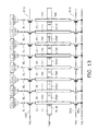
- FIG. 5 is a timing chart showing program operations in the semiconductor device according to the first embodiment.
- FIG. 6 is a flow chart showing a flow of “A-LEVEL PROGRAM”.
- FIG. 7 is a flow chart showing a flow of “B-LEVEL PROGRAM”.
- FIG. 8 is a flow chart showing a flow of “C-LEVEL PROGRAM”.
- Program information is inputted to the data buffer, from, for example, the host controller.
- the program information which is input to the data I/O buffer 203 , is output to the column control circuit 201 .
- a page buffer which transiently stores information by an amount stored in one page, is provided in the column control circuit.
- the program information is stored in the page buffer. Then, the program operations are started into the memory cells MC in the semiconductor device 200 .
- the program operations are sequentially performed in ascending order of threshold voltage, i.e. in order of “A-LEVEL PROGRAM”, “B-LEVEL PROGRAM” and “C-LEVEL PROGRAM”.
- threshold voltage i.e. in order of “A-LEVEL PROGRAM”, “B-LEVEL PROGRAM” and “C-LEVEL PROGRAM”.
- a voltage for selecting a program mode (hereinafter a program selection voltage Vss (Select)) is applied at a time t 1 in FIG. 5 to a bit line BL (A-level BL) connected to a memory cell MC that is programmed at A-LEVEL.
- a voltage for selecting an inhibit mode (hereinafter a program suppression voltage Vdd (Inhibit)) is applied at a time t 1 in FIG. 5 to bit lines BL (E-level BL, B-level BL and C-level BL).
- E-level BL is a bit line connected to a memory cell MC that is maintained at E-LEVEL
- B-level BL is a bit line connected to a memory cell MC that is programmed at B-LEVEL
- C-level BL is a bit line connected to a memory cell MC that is programmed at C-LEVEL.
- the voltage Vss may be, for example, an internal ground voltage
- the voltage Vdd is the one higher than the voltage Vss.
- the voltage Vdd may be, for example, an internal source voltage.
- the program selection voltage Vss (Select) is applied to the bit line BL corresponding to the memory cell MC that is programmed at A-LEVEL.
- the program suppression voltage Vdd (Inhibit) is applied to the bit line BL corresponding to the memory cell MC that is maintained at E-LEVEL or that is programmed at B-LEVEL or C-LEVEL.
- the program operations are stated (ST 3 in FIG. 6 ).
- the voltage Vss is applied to the source side selection gate line SGS; and the voltage Vdd is applied to the drain side selection gate line SGD.
- a passing voltage Vpass which makes memory cells MC turn on without relation to the threshold voltages held therein, is applied to word lines WL (WL 0 to WLn- 1 ).
- the voltages corresponding to the program information are applied via the bit lines BL 0 to BLm- 1 to the channels of memory cells MC corresponding to one page.
- the voltage Vss is applied to a channel of a memory cell MC that is programmed at A-LEVEL. Moreover, a voltage that is almost the same as the voltage Vdd is applied to the memory cells MC that are programmed at a level other than A-LEVEL.
- the voltages of the source side selection gate line SGS, the drain side selection gate line SGD and the word lines WL are controlled, for example, by the row control circuit 202 .
- the row control circuit 202 raises a voltage of one word line WL, which is selected from the word lines WL 0 to WLn- 1 , from the passing voltage Vpass to the programming voltage Vpgm that is higher than the passing voltage Vpass.
- charge injections into a charge storage portion occur in a memory cell MC in which the voltage Vss is applied to a channel, and shift the threshold voltage thereof, for example, in the positive direction.
- charge injections into a charge storage portion are suppressed in a memory cell MC in which the voltage Vdd is applied to the channel.
- a shift in the positive direction of the threshold voltage is suppressed therein.
- the memory cells MC in the semiconductor device 200 according to the first embodiment are three-dimensional structure type.
- FIG. 9 is a perspective view of the three-dimensional structure type memory cells.
- FIG. 10 is a perspective view of two-dimensional structure type memory cells MC.
- a three-dimensional structure type memory cell MC has a structure, for example, in which a channel 20 extends through a word line WL.
- the channel 20 is surrounded around 360 degrees, for example, via a memory film 30 by the word line WL.
- a channel 20 faces only one surface of a word line WL via a memory film 30 that includes a charge storage portion 30 as shown in FIG. 10 .
- a capacitance between the word line WL and channel 20 is structurally small comparing to the three-dimensional structure type memory cell MC.
- the two-dimensional structure type memory cells MC a plurality of memory cells MC arranged in one direction are provided with respect to one word line WL in contrast, in the three-dimensional structure type, a plurality of memory cells MC disposed in a tow-dimensional array, for example, in the X-Y directions are provided with respect to one word line WL.
- the number of memory cells MC connected to one word line WL is larger in the three-dimensional structure type memory cells MC than that in the two-dimensional structure type memory cells MC.
- An influence of parasitic capacitance between a word line WL and a channel 20 becomes significant in the three-dimensional structure type memory cells MC, since such a parasitic capacitance is structurally large in the three-dimensional structure type memory cells MC, whereas being ignored in the two-dimensional structure type memory cells MC.
- a variation range of RC time constants in word lines WL is large, which corresponds to data patterns equal to the amount of “one page” programmed in the program operation, comparing to the two-dimensional structure type memory cells MC.
- a RC time constant of a word line WL is large in the program operation, rise of voltage in the word line WL is delayed. Thereby, it becomes hard to program into the memory cell MC, and it influences on an operation rate in the programming.
- the voltage applied to a word line WL is set such that a programming pulse width and rise rate, for example, are adequate to a RC time constant in the worst case.
- a programming pulse width and rise rate for example, are adequate to a RC time constant in the worst case.
- it provides a case where excessive characteristics are achieved in a word line WL having a small RC time constant, and programming into a memory cell MC is excessively easy.
- erroneous programming such as programming or passing disturbance or over programming may be induced.
- FIGS. 11 and 12 are views showing a parasitic capacity between a word line WL and a channel 20 at a program operation.
- the program suppression voltage Vdd (Inhibit) is applied to bit lines BL.
- the program selection voltage Vss (Select) is applied to the bit lines BL.
- voltages of channels 20 are almost the same as the voltage Vdd, when the program suppression voltage Vss (Inhibit) is applied to the bit lines BL.
- the voltages of channels 20 are the same as the voltage Vss as shown in FIG. 12 , when the program selection voltage Vss (Select) is applied to the bit lines BL.
- the voltage difference between the word lines WL and the channels 20 also relate to the parasitic capacity between the word lines WL and the channels 20 .
- the parasitic capacity between the word lines WL and the channels 20 becomes maximum (e.g. see FIG. 12 ), when all voltages of channels 20 that correspond to “one page” are the voltage Vss.
- the total parasitic capacity between the word lines WL and the channels 20 is minimum value (e.g. see FIG. 11 ), when all voltages of channels 20 that correspond to “one page” are almost the same as the voltage Vdd.
- FIG. 13 is a view showing voltages in bit lines BL when starting A-LEVEL programming according to a comparative example.
- FIG. 14 is a view showing voltages in bit lines BL when starting A-LEVEL programming according to the first embodiment.
- a program operation is the one that causes a threshold voltage of a memory cell MC to be shifted.
- the program selection voltage Vss Select
- the program selection voltage Vss Select
- FIG. 13 the program selection voltage Vss (Select) is generally applied also to channels of memory cells MC in which programming is performed at B-LEVEL and C-LEVEL as shown in FIG. 13 .
- the program suppression voltage Vdd (Inhibit) is applied to the channels of memory cells MC in which programming is performed at B-LEVEL and C-LEVEL as shown in FIG. 14 .
- the memory cells MC are increased, in which the voltage of channels is almost the same as the voltage Vdd.
- the increase of the total parasitic capacity between the word lines WL and the cannel bodies 20 is suppressed in the program operation.
- a step ST 3 of the program operation shown in FIG. 6 is performed.
- the voltage of the selected word line WL is raised in the program operation from the passing voltage Vpass to the programming voltage Vpgm.
- electric charges are injected into the charge storage portion of the memory cell MC in which programming is performed at A-LEVEL, and the threshold voltage of the memory cell MC is shifted in the positive direction.
- a threshold voltage of a memory cell MC is verified whether being raised up to A-LEVEL or not.
- the verifying is carried out by performing a verify-read operation.
- the steps ST 3 and ST 4 are repeated until all threshold voltages of memory cells MC in which programming is performed at A-LEVEL are found to be A-LEVEL.
- the steps ST 3 and ST 4 are performed as a loop sequence, which is executed in parallel with respect to the memory cells corresponding to “one page”.
- the read operation is performed under a verify-read voltage Vva (see FIG. 4 ) applied to the selected word line WL (at a time t 1 in FIG. 5 ).
- Vva verify-read voltage
- the threshold voltage thereof is determined not to be raised up to A-LEVEL (determined not to pass, i.e. “NO”) at a step ST 5 .
- the program selection voltage Vss Select is applied to the bit line BL, and the threshold voltage thereof is shifted again in the next program operation.
- the threshold voltage thereof is determined to be raised up to A-LEVEL (pass at a step ST 5 , i.e. “YES”).
- the voltage of the bit line BL is changed from the program selection voltage Vss (Select) to the program suppression voltage Vdd (Inhibit). Thereby, the shift of the threshold voltage is suppressed in the next and following program operations.
- This voltage change in the bit line BL is performed, for example, by the column control circuit 201 .
- step ST 7 whether all bits pass or not is determined at a step ST 7 .
- step ST 8 whether the number of repetitions in the loop sequence reaches a prescribed number or not is determined at a step ST 8 .
- the steps ST 3 to ST 7 are repeated again after going back to the step ST 3 .
- the voltage of the bit line BL is changed from the program suppression voltage Vdd (Inhibit) to the program selection voltage Vss (Select) as shown in a step ST 11 .
- programming at B-LEVEL is started at a time t 2 shown in FIG. 5 with a delay by the prescribed number of the repetitions in the loop sequence from the start of programming at A-LEVEL.
- the steps ST 3 to ST 7 are repeated again.
- These voltage changes in the bit line BL are also performed, for example, by the column control circuit 201 .
- the program operation is performed after proceeding to a step ST 12 in FIG. 7 . Then, whether a threshold voltage of a memory cell MC is raised up to B-LEVEL or not is verified as shown in a step ST 13 .
- the verify-read operation of the step ST 13 the read operation is performed (at a time t 3 in FIG. 5 ) under a verify-read voltage Vvb (see FIG. 4 ) in the selected word line WL.
- the threshold voltage thereof is determined not to be raised up to B-LEVEL (determined not to pass, i.e. “NO”) at a step ST 14 .
- the column control circuit 201 applies the program selection voltage Vss (Select) to the bit line BL, and causes the threshold voltage to be shifted again in the next program operation.
- the threshold voltage is determined to be raised up to B-LEVEL (determined to pass, i.e. “YES”). Then, as shown in a step ST 15 , for example, the column control circuit 201 changes the voltage of the bit line BL from the program selection voltage Vss (Select) to the program suppression voltage Vdd (inhibit). Thereby, a shift of the threshold voltage is suppressed in the next and following program operations.
- step ST 16 whether all bits pass or not is determined.
- not passing i.e. “NO”
- whether the number of repetitions in a loop sequence reaches the prescribed number or not is determined.
- the steps ST 12 to ST 16 are repeated again.
- the column control circuit 201 applies the program suppression voltage Vdd (inhibit) to a bit line BL as shown in a step ST 19 . Thereafter, the steps ST 12 to ST 16 are repeated again.
- the column control circuit 201 When being determined to be programmed at C-LEVEL (i.e. “YES”), for example, the column control circuit 201 changes the voltage of the bit line BL from the program suppression voltage Vdd (inhibit) to the program selection voltage Vss (Select) as shown in a step ST 20 . Thereby, programming at C-LEVEL is started at a time t 4 in FIG. 5 with a delay by the prescribed number of the repetitions in the loop sequence from the start of programming at B-LEVEL. Then, the steps ST 12 to ST 16 are repeated again.
- the program operation is performed after proceeding to a step ST 21 in FIG. 8 . Then, whether a threshold voltage of a memory cell MC is raised up to C-LEVEL or not is verified as shown in a step ST 22 .
- a verify-read operation of the step ST 22 the read operation is preformed (at a time t 5 in FIG. 5 ) under a verify-read voltage Vvc (see FIG. 4 ) applied to the selected word line WL.
- Vvc verify-read voltage
- the threshold voltage thereof is determined not to be raised up to C-LEVEL (determined not to pass, i.e. “NO”) at a step ST 23 .
- the column control circuit 201 applies the program selection voltage Vss (Select) to a bit line BL. The threshold voltage is shifted again in the following program operation.
- the threshold voltage thereof is determined to be raised up to C-LEVEL (determined to pass, i.e. “YES”).
- the column control circuit 201 changes the voltage of the bit line BL from the program selection voltage Vss (Select) to the program suppression voltage Vdd (inhibit) as shown in a step ST 24 . A shift of the threshold voltage is suppressed in the next and following program operations.
- step ST 25 whether all bits pass or not is determined as shown in a step ST 25 .
- the steps ST 21 to ST 25 are repeated again.
- passing i.e. “YES”
- programming the information that corresponds to “one page” is ended (at a time t 6 in FIG. 5 ).
- the program selection voltage Vss (Select) is applied to a channel of the memory cell MC in which programming at A-LEVEL is performed
- the program suppression voltage Vdd (Inhibit) is applied to a channel of the memory cell MC in which programming at other than A-LEVEL is performed.
- the memory cells MC in which voltages of channels are almost the same as the voltage Vdd, are increased at an initial stage of the A-LEVEL programming.
- increase of parasitic capacity is suppressed between word lines WL and channels 20 .
- the RC time constant of word lines WL is suppressed to be small at the initial stage of A-LEVEL programming, it is possible to reduce a difference in the RC time constant between the worst case and the best case (i.e. a variation range of the RC time constant). Further, it is also possible to suppress a case where programming in a memory cell MC becomes excessively easy. Thus, according to the first embodiment, it is possible in the program operation to suppress an occurrence of erroneous programming such as disturbances in programming or passing, or programmed at a wrong level.
- timing of start in B-LEVEL programming or C-LEVEL programming is determined based on the number of repetitions in the loop sequence.
- the counter circuit counts, for example, the number of repetitions in the loop sequence.
- FIG. 15 is a flow chart showing A-LEVEL PROGRAM flow in a semiconductor device according to a second embodiment.
- the second embodiment is different in a step ST 8 a from the first embodiment.
- B-LEVEL programming starts with a delay by the prescribed number of the repetitions in the loop sequence from the start of A-LEVEL programming.
- B-LEVEL programming starts when the number of fail bits is reduced to be equal to or smaller than a prescribed value after the start of A-LEVEL programming.
- the “fail bits” correspond to bit lines BL that are connected respectively to memory cells MC in which threshold voltages are not raised up to A-LEVEL.
- the fail bits are determined in the verify-read operation (ST 4 , ST 5 ).
- the memory cells MC in which the threshold voltages are raised up to A-LEVEL are gradually increased by repeating the loop sequence including the steps ST 3 and ST 4 . Thereby, the memory cells MC having channels biased at the voltage Vdd are gradually increased, and the parasitic capacity is gradually lowered between word lines WL and channels 20 . In contrast, the number of fail bits is gradually reduced.
- proceeding to the step ST 9 is set to be triggered by the number of fail bits that is reduced to be equal to or smaller than a prescribed value, focusing on the number of residual fail bits.
- the B-LEVEL programming may start when the number of fail bits is equal to or smaller than a prescribed number after the start of A-LEVEL programming.
- proceeding to the step ST 18 may be set to be triggered by the number of fail bits being equal to or smaller than a prescribed value.
- the number of residual fail bits reflects an actual size of parasitic capacity in a more realistic way comparing to the number of repetitions in the loop sequence.
- accuracy comparing to the case, for example, based on the number of repetitions in the loop sequence.
Abstract
Description
Claims (20)
Priority Applications (1)
| Application Number | Priority Date | Filing Date | Title |
|---|---|---|---|
| US15/268,040 US9620222B1 (en) | 2016-03-02 | 2016-09-16 | Semiconductor device and method for operating the same |
Applications Claiming Priority (2)
| Application Number | Priority Date | Filing Date | Title |
|---|---|---|---|
| US201662302277P | 2016-03-02 | 2016-03-02 | |
| US15/268,040 US9620222B1 (en) | 2016-03-02 | 2016-09-16 | Semiconductor device and method for operating the same |
Publications (1)
| Publication Number | Publication Date |
|---|---|
| US9620222B1 true US9620222B1 (en) | 2017-04-11 |
Family
ID=58461805
Family Applications (1)
| Application Number | Title | Priority Date | Filing Date |
|---|---|---|---|
| US15/268,040 Active US9620222B1 (en) | 2016-03-02 | 2016-09-16 | Semiconductor device and method for operating the same |
Country Status (1)
| Country | Link |
|---|---|
| US (1) | US9620222B1 (en) |
Citations (6)
| Publication number | Priority date | Publication date | Assignee | Title |
|---|---|---|---|---|
| US7492634B2 (en) | 2005-10-27 | 2009-02-17 | Sandisk Corporation | Method for programming of multi-state non-volatile memory using smart verify |
| US20100238729A1 (en) * | 2009-03-23 | 2010-09-23 | Sanghyun Lee | Non-volatile memory with reduced leakage current for unselected blocks and method for operating same |
| US20110176367A1 (en) | 2010-01-20 | 2011-07-21 | Kabushiki Kaisha Toshiba | Nonvolatile semiconductor memory device and operation method thereof |
| JP2012160236A (en) | 2011-02-01 | 2012-08-23 | Toshiba Corp | Nonvolatile semiconductor memory device |
| US20130077409A1 (en) | 2011-09-22 | 2013-03-28 | Kabushiki Kaisha Toshiba | Nonvolatile semiconductor storage device |
| US20130141971A1 (en) | 2010-09-24 | 2013-06-06 | Koji Hosono | Nonvolatile semiconductor memory device |
-
2016
- 2016-09-16 US US15/268,040 patent/US9620222B1/en active Active
Patent Citations (8)
| Publication number | Priority date | Publication date | Assignee | Title |
|---|---|---|---|---|
| US7492634B2 (en) | 2005-10-27 | 2009-02-17 | Sandisk Corporation | Method for programming of multi-state non-volatile memory using smart verify |
| US20100238729A1 (en) * | 2009-03-23 | 2010-09-23 | Sanghyun Lee | Non-volatile memory with reduced leakage current for unselected blocks and method for operating same |
| US20110176367A1 (en) | 2010-01-20 | 2011-07-21 | Kabushiki Kaisha Toshiba | Nonvolatile semiconductor memory device and operation method thereof |
| JP2011150749A (en) | 2010-01-20 | 2011-08-04 | Toshiba Corp | Nonvolatile semiconductor memory device |
| US20130141971A1 (en) | 2010-09-24 | 2013-06-06 | Koji Hosono | Nonvolatile semiconductor memory device |
| JP2012160236A (en) | 2011-02-01 | 2012-08-23 | Toshiba Corp | Nonvolatile semiconductor memory device |
| US20130077409A1 (en) | 2011-09-22 | 2013-03-28 | Kabushiki Kaisha Toshiba | Nonvolatile semiconductor storage device |
| JP2013069373A (en) | 2011-09-22 | 2013-04-18 | Toshiba Corp | Nonvolatile semiconductor memory device |
Similar Documents
| Publication | Publication Date | Title |
|---|---|---|
| US8982626B2 (en) | Program and read operations for 3D non-volatile memory based on memory hole diameter | |
| US10014063B2 (en) | Smart skip verify mode for programming a memory device | |
| US9830983B1 (en) | Memory system and writing method | |
| JP5172555B2 (en) | Semiconductor memory device | |
| KR101929087B1 (en) | Erase operation for 3d non volatile memory with controllable gate-induced drain leakage current | |
| US9659663B2 (en) | Semiconductor memory device | |
| JP5524134B2 (en) | Nonvolatile semiconductor memory device | |
| KR102606826B1 (en) | Nonvolatile memory devices and erasing method of the same | |
| US10566039B2 (en) | Memory device | |
| US20140362642A1 (en) | 3D Non-Volatile Memory With Control Gate Length Based On Memory Hole Diameter | |
| US10720208B2 (en) | Semiconductor memory device | |
| US10971240B1 (en) | Wordline smart tracking verify | |
| US20160019971A1 (en) | Nonvolatile semiconductor memory device and method of controlling the same | |
| KR20210101311A (en) | Non-volatile memory device and control method | |
| JP2010287283A (en) | Nonvolatile semiconductor memory | |
| US10424384B2 (en) | Semiconductor memory device and control method of semiconductor memory device | |
| TWI633552B (en) | Semiconductor memory device and method of controlling the same | |
| US20150262679A1 (en) | Semiconductor memory device and method of controlling the same | |
| US20210391012A1 (en) | Neighbor aware multi-bias programming in scaled bics | |
| JP7132444B2 (en) | Method for reducing program disturbance in memory device and memory device using the same | |
| CN110998734A (en) | Memory device capable of reducing program disturb and erasing method thereof | |
| US11605437B2 (en) | Memory programming with selectively skipped verify pulses for performance improvement | |
| US9620222B1 (en) | Semiconductor device and method for operating the same | |
| US10176874B2 (en) | Storage device and method of controlling the storage device | |
| US11468950B1 (en) | Memory programming with selectively skipped bitscans and fewer verify pulses for performance improvement |
Legal Events
| Date | Code | Title | Description |
|---|---|---|---|
| AS | Assignment |
Owner name: KABUSHIKI KAISHA TOSHIBA, JAPAN Free format text: ASSIGNMENT OF ASSIGNORS INTEREST;ASSIGNORS:MINEMURA, YOICHI;SHIMURA, YASUHIRO;SIGNING DATES FROM 20161104 TO 20161110;REEL/FRAME:040757/0502 |
|
| STCF | Information on status: patent grant |
Free format text: PATENTED CASE |
|
| AS | Assignment |
Owner name: TOSHIBA MEMORY CORPORATION, JAPAN Free format text: ASSIGNMENT OF ASSIGNORS INTEREST;ASSIGNOR:KABUSHIKI KAISHA TOSHIBA;REEL/FRAME:043709/0035 Effective date: 20170706 |
|
| MAFP | Maintenance fee payment |
Free format text: PAYMENT OF MAINTENANCE FEE, 4TH YEAR, LARGE ENTITY (ORIGINAL EVENT CODE: M1551); ENTITY STATUS OF PATENT OWNER: LARGE ENTITY Year of fee payment: 4 |
|
| AS | Assignment |
Owner name: K.K. PANGEA, JAPAN Free format text: MERGER;ASSIGNOR:TOSHIBA MEMORY CORPORATION;REEL/FRAME:055659/0471 Effective date: 20180801 Owner name: TOSHIBA MEMORY CORPORATION, JAPAN Free format text: CHANGE OF NAME AND ADDRESS;ASSIGNOR:K.K. PANGEA;REEL/FRAME:055669/0401 Effective date: 20180801 Owner name: KIOXIA CORPORATION, JAPAN Free format text: CHANGE OF NAME AND ADDRESS;ASSIGNOR:TOSHIBA MEMORY CORPORATION;REEL/FRAME:055669/0001 Effective date: 20191001 |