US9617618B2 - Silicon purification mold and method - Google Patents
Silicon purification mold and method Download PDFInfo
- Publication number
- US9617618B2 US9617618B2 US14/375,743 US201314375743A US9617618B2 US 9617618 B2 US9617618 B2 US 9617618B2 US 201314375743 A US201314375743 A US 201314375743A US 9617618 B2 US9617618 B2 US 9617618B2
- Authority
- US
- United States
- Prior art keywords
- crucible
- silicon
- temperature
- molten metal
- alloy
- Prior art date
- Legal status (The legal status is an assumption and is not a legal conclusion. Google has not performed a legal analysis and makes no representation as to the accuracy of the status listed.)
- Expired - Fee Related, expires
Links
- 238000000034 method Methods 0.000 title claims abstract description 60
- 229910052710 silicon Inorganic materials 0.000 title claims description 94
- 239000010703 silicon Substances 0.000 title claims description 94
- XUIMIQQOPSSXEZ-UHFFFAOYSA-N Silicon Chemical compound [Si] XUIMIQQOPSSXEZ-UHFFFAOYSA-N 0.000 title description 84
- 238000000746 purification Methods 0.000 title description 11
- 238000001816 cooling Methods 0.000 claims abstract description 30
- 230000005496 eutectics Effects 0.000 claims description 32
- 229910001092 metal group alloy Inorganic materials 0.000 claims description 30
- 238000010438 heat treatment Methods 0.000 claims description 25
- 239000000956 alloy Substances 0.000 claims description 17
- 229910045601 alloy Inorganic materials 0.000 claims description 15
- CSDREXVUYHZDNP-UHFFFAOYSA-N alumanylidynesilicon Chemical compound [Al].[Si] CSDREXVUYHZDNP-UHFFFAOYSA-N 0.000 claims description 11
- 239000000203 mixture Substances 0.000 claims description 10
- 229910000838 Al alloy Inorganic materials 0.000 claims description 9
- 229910052782 aluminium Inorganic materials 0.000 claims description 9
- XAGFODPZIPBFFR-UHFFFAOYSA-N aluminium Chemical compound [Al] XAGFODPZIPBFFR-UHFFFAOYSA-N 0.000 claims description 9
- 239000004020 conductor Substances 0.000 claims 2
- 239000000463 material Substances 0.000 abstract description 15
- 238000007711 solidification Methods 0.000 abstract description 14
- 230000008023 solidification Effects 0.000 abstract description 14
- 239000002210 silicon-based material Substances 0.000 abstract description 2
- 239000012535 impurity Substances 0.000 description 17
- 239000011343 solid material Substances 0.000 description 13
- 229910000676 Si alloy Inorganic materials 0.000 description 12
- 239000007788 liquid Substances 0.000 description 10
- 239000012768 molten material Substances 0.000 description 10
- 239000012071 phase Substances 0.000 description 7
- 229910052751 metal Inorganic materials 0.000 description 6
- 239000002184 metal Substances 0.000 description 6
- 239000013078 crystal Substances 0.000 description 4
- 238000009413 insulation Methods 0.000 description 4
- 239000000155 melt Substances 0.000 description 4
- HBMJWWWQQXIZIP-UHFFFAOYSA-N silicon carbide Chemical compound [Si+]#[C-] HBMJWWWQQXIZIP-UHFFFAOYSA-N 0.000 description 4
- 239000007858 starting material Substances 0.000 description 4
- 238000010587 phase diagram Methods 0.000 description 3
- 229910010271 silicon carbide Inorganic materials 0.000 description 3
- 230000008901 benefit Effects 0.000 description 2
- 238000010586 diagram Methods 0.000 description 2
- 238000004519 manufacturing process Methods 0.000 description 2
- 239000002244 precipitate Substances 0.000 description 2
- 230000001376 precipitating effect Effects 0.000 description 2
- 238000011403 purification operation Methods 0.000 description 2
- 239000007790 solid phase Substances 0.000 description 2
- 238000005406 washing Methods 0.000 description 2
- 239000002253 acid Substances 0.000 description 1
- 230000006978 adaptation Effects 0.000 description 1
- 229910002056 binary alloy Inorganic materials 0.000 description 1
- 230000015572 biosynthetic process Effects 0.000 description 1
- 238000006243 chemical reaction Methods 0.000 description 1
- 229910021419 crystalline silicon Inorganic materials 0.000 description 1
- 238000002425 crystallisation Methods 0.000 description 1
- 230000008025 crystallization Effects 0.000 description 1
- 238000000151 deposition Methods 0.000 description 1
- 239000006023 eutectic alloy Substances 0.000 description 1
- 230000001747 exhibiting effect Effects 0.000 description 1
- 239000013072 incoming material Substances 0.000 description 1
- 230000001939 inductive effect Effects 0.000 description 1
- 238000012986 modification Methods 0.000 description 1
- 230000004048 modification Effects 0.000 description 1
- 238000001556 precipitation Methods 0.000 description 1
- 230000002250 progressing effect Effects 0.000 description 1
- 239000011819 refractory material Substances 0.000 description 1
- 229910052594 sapphire Inorganic materials 0.000 description 1
- 239000010980 sapphire Substances 0.000 description 1
- 239000004065 semiconductor Substances 0.000 description 1
- 239000007787 solid Substances 0.000 description 1
Images


Classifications
-
- C—CHEMISTRY; METALLURGY
- C22—METALLURGY; FERROUS OR NON-FERROUS ALLOYS; TREATMENT OF ALLOYS OR NON-FERROUS METALS
- C22B—PRODUCTION AND REFINING OF METALS; PRETREATMENT OF RAW MATERIALS
- C22B9/00—General processes of refining or remelting of metals; Apparatus for electroslag or arc remelting of metals
-
- C—CHEMISTRY; METALLURGY
- C01—INORGANIC CHEMISTRY
- C01B—NON-METALLIC ELEMENTS; COMPOUNDS THEREOF; METALLOIDS OR COMPOUNDS THEREOF NOT COVERED BY SUBCLASS C01C
- C01B33/00—Silicon; Compounds thereof
- C01B33/02—Silicon
-
- C—CHEMISTRY; METALLURGY
- C01—INORGANIC CHEMISTRY
- C01B—NON-METALLIC ELEMENTS; COMPOUNDS THEREOF; METALLOIDS OR COMPOUNDS THEREOF NOT COVERED BY SUBCLASS C01C
- C01B33/00—Silicon; Compounds thereof
- C01B33/02—Silicon
- C01B33/037—Purification
-
- C—CHEMISTRY; METALLURGY
- C22—METALLURGY; FERROUS OR NON-FERROUS ALLOYS; TREATMENT OF ALLOYS OR NON-FERROUS METALS
- C22B—PRODUCTION AND REFINING OF METALS; PRETREATMENT OF RAW MATERIALS
- C22B21/00—Obtaining aluminium
- C22B21/06—Obtaining aluminium refining
-
- C—CHEMISTRY; METALLURGY
- C30—CRYSTAL GROWTH
- C30B—SINGLE-CRYSTAL GROWTH; UNIDIRECTIONAL SOLIDIFICATION OF EUTECTIC MATERIAL OR UNIDIRECTIONAL DEMIXING OF EUTECTOID MATERIAL; REFINING BY ZONE-MELTING OF MATERIAL; PRODUCTION OF A HOMOGENEOUS POLYCRYSTALLINE MATERIAL WITH DEFINED STRUCTURE; SINGLE CRYSTALS OR HOMOGENEOUS POLYCRYSTALLINE MATERIAL WITH DEFINED STRUCTURE; AFTER-TREATMENT OF SINGLE CRYSTALS OR A HOMOGENEOUS POLYCRYSTALLINE MATERIAL WITH DEFINED STRUCTURE; APPARATUS THEREFOR
- C30B11/00—Single-crystal growth by normal freezing or freezing under temperature gradient, e.g. Bridgman-Stockbarger method
- C30B11/002—Crucibles or containers for supporting the melt
-
- C—CHEMISTRY; METALLURGY
- C30—CRYSTAL GROWTH
- C30B—SINGLE-CRYSTAL GROWTH; UNIDIRECTIONAL SOLIDIFICATION OF EUTECTIC MATERIAL OR UNIDIRECTIONAL DEMIXING OF EUTECTOID MATERIAL; REFINING BY ZONE-MELTING OF MATERIAL; PRODUCTION OF A HOMOGENEOUS POLYCRYSTALLINE MATERIAL WITH DEFINED STRUCTURE; SINGLE CRYSTALS OR HOMOGENEOUS POLYCRYSTALLINE MATERIAL WITH DEFINED STRUCTURE; AFTER-TREATMENT OF SINGLE CRYSTALS OR A HOMOGENEOUS POLYCRYSTALLINE MATERIAL WITH DEFINED STRUCTURE; APPARATUS THEREFOR
- C30B11/00—Single-crystal growth by normal freezing or freezing under temperature gradient, e.g. Bridgman-Stockbarger method
- C30B11/003—Heating or cooling of the melt or the crystallised material
-
- C—CHEMISTRY; METALLURGY
- C30—CRYSTAL GROWTH
- C30B—SINGLE-CRYSTAL GROWTH; UNIDIRECTIONAL SOLIDIFICATION OF EUTECTIC MATERIAL OR UNIDIRECTIONAL DEMIXING OF EUTECTOID MATERIAL; REFINING BY ZONE-MELTING OF MATERIAL; PRODUCTION OF A HOMOGENEOUS POLYCRYSTALLINE MATERIAL WITH DEFINED STRUCTURE; SINGLE CRYSTALS OR HOMOGENEOUS POLYCRYSTALLINE MATERIAL WITH DEFINED STRUCTURE; AFTER-TREATMENT OF SINGLE CRYSTALS OR A HOMOGENEOUS POLYCRYSTALLINE MATERIAL WITH DEFINED STRUCTURE; APPARATUS THEREFOR
- C30B29/00—Single crystals or homogeneous polycrystalline material with defined structure characterised by the material or by their shape
- C30B29/02—Elements
- C30B29/06—Silicon
-
- F—MECHANICAL ENGINEERING; LIGHTING; HEATING; WEAPONS; BLASTING
- F27—FURNACES; KILNS; OVENS; RETORTS
- F27B—FURNACES, KILNS, OVENS OR RETORTS IN GENERAL; OPEN SINTERING OR LIKE APPARATUS
- F27B14/00—Crucible or pot furnaces
- F27B14/08—Details specially adapted for crucible or pot furnaces
- F27B14/14—Arrangements of heating devices
-
- F—MECHANICAL ENGINEERING; LIGHTING; HEATING; WEAPONS; BLASTING
- F27—FURNACES; KILNS; OVENS; RETORTS
- F27B—FURNACES, KILNS, OVENS OR RETORTS IN GENERAL; OPEN SINTERING OR LIKE APPARATUS
- F27B14/00—Crucible or pot furnaces
- F27B14/08—Details specially adapted for crucible or pot furnaces
- F27B14/20—Arrangement of controlling, monitoring, alarm or like devices
Definitions
- Solar cells can be a viable energy source by utilizing their ability to convert sunlight to electrical energy.
- Silicon is a semiconductor material and the raw incoming material used in the manufacture of solar cells. The electrical properties of the cells, namely the conversion efficiency depends on the purity of the silicon.
- Several techniques have been used to purify silicon. The most well known technique is called ‘Siemens process.’ This technique removes substantially all impurities present within the silicon. However, this technique requires production of the silicon in a gas phase and re-depositing into a solid phase in order to remove the impurities. Other techniques include zone refinement, and directional solidification.
- a method of silicon purification may include cooling a molten silicon alloy, and precipitating silicon crystals from the molten alloy, leaving impurities in the remaining melt.
- a method of silicon purification may then include separating the precipitated silicon from the molten metal alloy.
- a method in Example 1, includes forming a molten metal alloy in a crucible, wherein the alloy forms a binary eutectic system with silicon. The method also includes cooling at least a portion of the molten metal alloy to a temperature below a liquidus temperature and above a eutectic temperature to precipitate silicon from the molten metal alloy, controlling temperature within the crucible to maintain a minimum temperature above the eutectic temperature within the crucible, and separating the precipitated silicon from the molten metal alloy.
- Example 4 the method of any one or any combination of Examples 1-3 is optionally configured such that forming a molten metal alloy in a crucible includes forming silicon-aluminum alloy in a starting composition between approximately 60 wt. % silicon and 22 wt. % silicon, with a balance being substantially aluminum.
- Example 6 the method of any one or any combination of Examples 1-5 is optionally configured such that cooling includes maintaining a temperature within the crucible in a range between approximately 577° C.-1100° C.
- Example 7 the method of any one or any combination of Examples 1-6 is optionally configured such that cooling includes maintaining a temperature within the crucible in a range between approximately 720° C.-1100° C.
- Example 8 the method of any one or any combination of Examples 1-7 is optionally configured such that cooling includes maintaining a temperature within the crucible in a range between approximately 650° C.-960° C.
- Example 9 the method of any one or any combination of Examples 1-8 is optionally configured such that controlling temperature within the crucible includes covering a top of the crucible.
- Example 11 the method of Example 10 is optionally configured such that forming a molten metal alloy in a crucible includes forming a silicon-aluminum alloy in a crucible.
- Example 13 the method of any one or any combination of Examples 10-12 is optionally configured such that actively heating the crucible includes heating sides of the crucible.
- a silicon purification system includes a crucible, including a plurality of crucible lining layers, a heating system located adjacent to the crucible to control temperature within at least a portion of the crucible, and a heating system controller configured to maintain a minimum temperature within the crucible above a binary silicon alloy eutectic temperature, when in operation.
- Example 16 the system of Example 15 is optionally configured such that the heating system includes a top heater.
- Example 17 the system of any one or any combination of Examples 15-16 is optionally configured such that the top heater includes a refractory layer within a metal shell.
- Example 18 the system of any one or any combination of Examples 15-17 is optionally configured such that the heating system includes side heaters.
- Example 20 the system of any one or any combination of Examples 15-19 is optionally configured such that the plurality of crucible lining layers includes a metal shell with refractory lining, with SiC bottom layer.
- Example 22 the system of any one or any combination of Examples 15-21 is optionally configured such that the heating system controller is configured to operate within a range between approximately 720° C.-1100° C.
- Example 23 the system of any one or any combination of Examples 15-22 is optionally configured to further include a scoop system to remove precipitated silicon from within a molten binary silicon alloy.
- FIG. 1 shows a binary phase diagram according to at least one embodiment of the invention.
- FIG. 2 shows a cross section of a mold according to at least one embodiment of the invention.
- FIG. 3 shows a cross section of a mold according to at least one embodiment of the invention.
- FIG. 4 shows a cross section of a system according to at least one embodiment of the invention.
- FIGS. 5A-5D show a series of modeled cooling profiles for silicon using a mold according to at least one embodiment of the invention.
- FIGS. 6A-6E show another series of modeled cooling profiles for silicon using a mold according to at least one embodiment of the invention.
- FIG. 7 shows a flow diagram of an example method according to at least one embodiment of the invention.
- references in the specification to “one embodiment”, “an embodiment”, “an example embodiment”, etc., indicate that the embodiment described can include a particular feature, structure, or characteristic, but every embodiment may not necessarily include the particular feature, structure, or characteristic. Moreover, such phrases are not necessarily referring to the same embodiment. Further, when a particular feature, structure, or characteristic is described in connection with an embodiment, it is submitted that it is within the knowledge of one skilled in the art to affect such feature, structure, or characteristic in connection with other embodiments whether or not explicitly described.
- the present subject matter relates to molds, mold systems, and related methods for purifying silicon using fractional solidification techniques.
- the purified silicon resulting from the fractional solidification can be used in solar cells. It has been found that by controlling the temperature and temperature gradient within the mold, a highly controlled fractional solidification can be accomplished.
- purification of silicon is described in the most detail in examples below, systems and methods described can also be used for fractional solidification and purification of other materials such as sapphire.
- a molten silicon alloy is formed using a silicon starting material that includes impurities. Silicon is precipitated (e.g. fractionally solidified) from the molten silicon alloy in a purification process.
- the molten silicon alloy is a binary alloy, although the invention is not so limited.
- impurities from the silicon starting material remain in an amount of remaining molten alloy, while the precipitated silicon is substantially pure.
- the molten silicon alloy is a binary silicon-aluminum alloy, as described below.
- FIG. 1 illustrates a binary phase diagram of silicon and aluminum.
- the X-axis indicates the amount of silicon in an alloy, indicated in units of weight percent (wt. %).
- a 100% aluminum material is indicated, with zero wt. % silicon.
- a 100% silicon material is indicated, with zero wt % aluminum.
- a solidus line 106 is shown at the eutectic temperature of 577° C. for aluminum-silicon, with a eutectic point 108 indicated at the eutectic temperature and a composition of approximately 12.6 wt. % silicon.
- a liquidus line 110 is shown progressing downward from a temperature of approximately 1414° C. for pure silicon to 577° C. at the eutectic point.
- a composition range 112 is also shown in FIG. 1 , from approximately 60 wt. % silicon to approximately 22 wt. % silicon. In one example, the composition range 112 is from approximately 42 wt. % silicon to approximately 22 wt. % silicon. In one example, an initial composition begins at a silicon wt. % higher than 22 wt. % and progresses from a temperature above the liquidus line 110 for the selected composition. As cooling progresses in the crucible, and the temperature crosses the liquidus line 110 , crystalline silicon flakes begin to form in the melt, and the composition of the remaining liquid progresses down the liquidus line as illustrated by arrow 126 . For example, an initial concentration of alloy, with a silicon concentration of 60 wt.
- Impurities that may have been present in silicon starting material may substantially or completely remain in the liquid fraction, while the precipitated silicon flakes are substantially pure silicon.
- the silicon flakes may be collected and separated from the remaining melt. In this way, impurities in a silicon starting material may be removed to yield substantially pure silicon.
- the collected silicon flakes may be further processed to remove any remaining impurities, or they may be melted and re-formed to make electronic devices, such as photovoltaic devices.
- further processing to remove any remaining impurities may include iteratively performing the fractional solidification technique described above.
- further processing to remove any remaining impurities may include washing the silicon flakes to remove any molten alloy residue.
- washing may include an acid wash operation.
- other processing techniques may be used in addition to the fractional solidification technique described above, for example directional solidification may be used either before or after the fractional solidification technique described.
- the silicon is melted and re-formed to make electronic devices, such as photovoltaic devices.
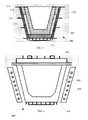
- FIG. 2 illustrates a crucible 200 having sides 202 and a bottom 204 .
- a number of silicon flakes 206 are illustrated, with a remaining liquid portion 208 .
- a dashed line 210 is shown to indicate a zone 212 of silicon flakes formed adjacent to sides 202 of the crucible 200 , and a zone 214 of silicon flakes in a middle portion of the crucible 200 .
- a lamellar microstructure is not desirable, because it contains multiple layers of silicon and aluminum sandwiched together in a configuration where it is difficult to separate the silicon from the aluminum. It is desirable to increase a fraction of silicon flakes precipitating out of the melt, while not cooling the melt below the eutectic temperature.
- the silicon flakes 206 are separated from the liquid portion 208 .
- separating includes collecting the silicon flakes 206 and removing them from the liquid portion 208 .
- the liquid portion 208 is poured off, and the silicon flakes 206 remain in the crucible for collection.
- FIG. 3 shows a crucible 300 according to an embodiment of the invention.
- a number of different material layers are shown housed within a metal shell 306 .
- a number of fins 308 are coupled to the metal shell 306 .
- the fins 308 provide increased surface area for heat transfer.
- the fins 308 provide structural support and handling surfaces for the metal shell 306 .
- material 312 includes a heat conduction property of approximately 0.20 W/(mK).
- material 314 includes a heat conduction property of approximately 0.05 W/(mK).
- at least bottom portion 312 includes a material that includes a heat conduction property of approximately 8 W/(mK).
- the bottom portion 312 includes silicon carbide (SiC).
- the melt within the crucible 300 is cooled preferentially from the bottom.
- Configurations including SiC in a bottom portion 312 are adapted to cool preferentially from the bottom.
- FIG. 4 illustrates a system 400 according to an embodiment of the invention.
- a crucible 401 is shown.
- the crucible 401 is similar to crucible 300 as illustrated in FIG. 3 .
- the system 400 includes a cover 402 .
- the cover is adapted to retain heat within the crucible 401 during cooling.
- the cover 402 includes insulating layers within a metal shell.
- the cover provides passive insulation during a cooling operation.
- the cover 402 includes one or more heating elements, such as resistive heating elements.
- a temperature of a top of the crucible 401 is controlled using either passive insulation or active heating elements, while a bottom of the crucible 401 is preferentially cooled, for example using a material with a higher thermal conductivity than walls or a cover 402 of the system.
- walls of the crucible 401 are heated using one or more side heaters 404 .
- Side heaters 404 shown in FIG. 4 include a number of resistive heating elements 406 that are used to control a temperature in walls of the crucible 401 .
- the side heaters 404 also include additional insulation such as refractory material to maintain temperature in walls of the crucible 401 .
- the system 400 provides a number of temperature controls over the crucible 401 .
- One control includes an ability to control temperatures of selected surfaces to prevent or reduce unwanted eutectic phase growth.
- Another control includes an ability to control a temperature gradient within the crucible. A more consistent temperature gradient may provide higher silicon flake precipitation efficiency, and higher yield. If the molten alloy in the crucible is maintained at a consistent temperature with a tight thermal gradient close to the eutectic temperature, then more silicon will precipitate, and less unwanted eutectic phase will form.
- surfaces such as the top surface, and wall surfaces are controlled separately to provide optimum surface temperature control.
- the bottom of the crucible 401 is allowed to cool more quickly, as a result of factors such as a higher thermal conductivity material in the bottom of the crucible 401 , and an absence of any active heating elements adjacent to the bottom of the crucible 401 . Selected advantages of cooling a bottom of the crucible 401 more quickly are discussed in more detail below.
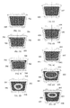
- FIGS. 5A-5D illustrate modeled cooling of molten alloy 502 within a crucible 500 without elements such as side heaters, a top cover, or a top heater.
- the crucible 500 modeled in FIGS. 5A-5D does not include a bottom material with a higher thermal conductivity than walls of the crucible.
- substantially all of the alloy material within the crucible 500 is a molten silicon alloy 502 .
- FIG. 5B after cooling, an amount of solid material 501 has formed at a top surface 504 and on sides 506 of the crucible 500 , with an amount of molten alloy 502 remaining within a center of the crucible 500 . A bottom 508 of the crucible remains substantially molten.
- FIG. 5C illustrates progression of solid material 501 at the top 504 and sides 506 of the crucible.
- the bottom 508 remains substantially molten, along with the center of the crucible 500 .
- FIG. 5D the fraction of solid material within the crucible has substantially increased, with the top 504 , sides 506 , and bottom 508 all forming solid material 501 , and the remaining molten portion 502 being located in a middle of the crucible.
- the remaining molten portion 502 is trapped within the crucible Impurities that remain in the remaining molten portion 502 may be difficult to separate from the rest of the solid portion within the crucible.
- FIGS. 6A-6E illustrate modeled cooling of molten alloy 602 within a crucible 600 according to one or more embodiments of the invention, including features such as side heaters, top covers, top heaters, and a bottom that is more thermally conductive than sides of the crucible 600 .
- substantially all of the alloy material within the crucible 600 is a molten silicon alloy 602 .
- an amount of solid material 601 has formed at the bottom 608 with a small amount of solid material 601 forming along sides 606 of the crucible 600 .
- a more conductive layer, such as silicon carbide, in the bottom 608 of the crucible encourages preferential cooling on the bottom 608 .
- the top 604 and center of the crucible 600 remains substantially molten.
- FIG. 6C illustrates progression of solid material 601 at the bottom 608 , with minimal progression at the sides 606 and substantially no progression at the top 604 of the crucible 600 .
- FIG. 6D the fraction of solid material 601 within the crucible has substantially increased, primarily from the bottom 608 , upwards towards the top 604 and to some extent, from the sides 606 .
- the top 604 remains substantially molten material 602 .
- the solid material 601 consists primarily of silicon that has precipitated out of the molten material 602 , at a temperature above the eutectic temperature of the silicon alloy. Utilizing features such as passive heat insulation, and/or active heaters on surfaces such as a top 604 and sides 606 of the crucible, temperature within the crucible is tightly controlled.
- the molten material 602 may be poured out of the crucible 600 .
- the solid material 601 may be scooped out of the crucible 600 using a scoop system, such as a sieve, or slotted scoop, or blade, etc.
- a combination of pouring off molten material 602 and scooping out purified solid material 601 may be used. As discussed in examples above, impurities will stay in solution in the molten material 602 , while the precipitated silicon solid material 601 is substantially pure.
- FIG. 7 illustrates a flow diagram of a method as described from selected examples above.
- a molten metal alloy is formed in a crucible to form a binary eutectic alloy with silicon.
- one alloy includes an aluminum-silicon alloy.
- at least a portion of the molten metal alloy is cooled to a temperature below a liquidus temperature and above a eutectic temperature to precipitate silicon from the molten metal alloy.
- temperature is controlled within the crucible to maintain a minimum temperature above the eutectic temperature within the crucible, and in operation 708 , the precipitated silicon is separated from the molten metal alloy.
Landscapes
- Chemical & Material Sciences (AREA)
- Engineering & Computer Science (AREA)
- Organic Chemistry (AREA)
- Materials Engineering (AREA)
- Metallurgy (AREA)
- Mechanical Engineering (AREA)
- Crystallography & Structural Chemistry (AREA)
- General Engineering & Computer Science (AREA)
- Inorganic Chemistry (AREA)
- Manufacturing & Machinery (AREA)
- Silicon Compounds (AREA)
Abstract
Description
Claims (11)
Priority Applications (1)
| Application Number | Priority Date | Filing Date | Title |
|---|---|---|---|
| US14/375,743 US9617618B2 (en) | 2012-02-01 | 2013-02-01 | Silicon purification mold and method |
Applications Claiming Priority (3)
| Application Number | Priority Date | Filing Date | Title |
|---|---|---|---|
| US201261593573P | 2012-02-01 | 2012-02-01 | |
| US14/375,743 US9617618B2 (en) | 2012-02-01 | 2013-02-01 | Silicon purification mold and method |
| PCT/US2013/024333 WO2013116640A1 (en) | 2012-02-01 | 2013-02-01 | Silicon purification mold and method |
Publications (2)
| Publication Number | Publication Date |
|---|---|
| US20150128764A1 US20150128764A1 (en) | 2015-05-14 |
| US9617618B2 true US9617618B2 (en) | 2017-04-11 |
Family
ID=47716173
Family Applications (1)
| Application Number | Title | Priority Date | Filing Date |
|---|---|---|---|
| US14/375,743 Expired - Fee Related US9617618B2 (en) | 2012-02-01 | 2013-02-01 | Silicon purification mold and method |
Country Status (8)
| Country | Link |
|---|---|
| US (1) | US9617618B2 (en) |
| EP (1) | EP2809615A1 (en) |
| JP (1) | JP6177805B2 (en) |
| KR (1) | KR102044450B1 (en) |
| CN (2) | CN110054189A (en) |
| BR (1) | BR112014018669A2 (en) |
| TW (1) | TWI627131B (en) |
| WO (1) | WO2013116640A1 (en) |
Cited By (1)
| Publication number | Priority date | Publication date | Assignee | Title |
|---|---|---|---|---|
| RU2702173C1 (en) * | 2018-12-25 | 2019-10-04 | Федеральное государственное бюджетное образовательное учреждение высшего образования "Рязанский государственный радиотехнический университет" | Method of improving silicon purification efficiency |
Families Citing this family (3)
| Publication number | Priority date | Publication date | Assignee | Title |
|---|---|---|---|---|
| TWI627131B (en) | 2012-02-01 | 2018-06-21 | 美商希利柯爾材料股份有限公司 | 矽Purification mold and method |
| CN107585770A (en) * | 2016-12-07 | 2018-01-16 | 安徽爱森能源有限公司 | A kind of method of purification of silicon |
| CN106914609B (en) * | 2017-04-27 | 2019-06-28 | 重庆大学 | A kind of aluminum alloy melt heating and heat preservation method |
Citations (14)
| Publication number | Priority date | Publication date | Assignee | Title |
|---|---|---|---|---|
| US3069240A (en) | 1958-01-24 | 1962-12-18 | Electro Chimie Metal | Method of obtaining pure silicon by fractional crystallization |
| JPS5622620A (en) | 1979-05-24 | 1981-03-03 | Aluminum Co Of America | Silicon purification |
| US4312847A (en) * | 1979-05-24 | 1982-01-26 | Aluminum Company Of America | Silicon purification system |
| WO2007112592A1 (en) | 2006-04-04 | 2007-10-11 | 6N Silicon Inc. | Method for purifying silicon |
| US20090092535A1 (en) | 2007-10-03 | 2009-04-09 | Scott Nichol | Method for processing silicon powder to obtain silicon crystals |
| CN101479410A (en) | 2006-06-23 | 2009-07-08 | Rec斯坎沃佛股份有限公司 | Method and crucible for directional solidification of semiconductor grade polycrystalline silicon ingots |
| EP2138610A1 (en) | 2007-03-19 | 2009-12-30 | Mnk-sog Silicon, Inc. | Method and apparatus for manufacturing silicon ingot |
| US20100163550A1 (en) * | 2008-12-26 | 2010-07-01 | Belsh Joseph T | Heating and Melting of Materials by Electric Induction Heating of Susceptors |
| WO2011020197A1 (en) | 2009-08-21 | 2011-02-24 | 6N Silicon Inc. | Method of purifying silicon utilizing cascading process |
| GB2479165A (en) | 2009-10-14 | 2011-10-05 | Rec Wafer Norway As | Reusable crucible |
| US20110302963A1 (en) | 2009-02-26 | 2011-12-15 | Harsharn Tathgar | Method for the production of solar grade silicon |
| US20120297580A1 (en) * | 2009-10-21 | 2012-11-29 | Fabrizio Dughiero | Method and device for obtaining a multicrystalline semiconductor material, in particular silicon |
| TW201345837A (en) | 2012-02-01 | 2013-11-16 | Silicor Materials Inc | 矽Purification mold and method |
| US9054249B2 (en) | 2008-05-28 | 2015-06-09 | Solar—Tectic LLC | Methods of growing heteroepitaxial single crystal or large grained semiconductor films and devices thereon |
Family Cites Families (3)
| Publication number | Priority date | Publication date | Assignee | Title |
|---|---|---|---|---|
| US4193975A (en) * | 1977-11-21 | 1980-03-18 | Union Carbide Corporation | Process for the production of improved refined metallurgical silicon |
| US4643833A (en) * | 1984-05-04 | 1987-02-17 | Siemens Aktiengesellschaft | Method for separating solid reaction products from silicon produced in an arc furnace |
| FR2827592B1 (en) * | 2001-07-23 | 2003-08-22 | Invensil | HIGH PURITY METALLURGICAL SILICON AND PROCESS FOR PRODUCING THE SAME |
-
2013
- 2013-01-28 TW TW102103094A patent/TWI627131B/en not_active IP Right Cessation
- 2013-02-01 CN CN201811547031.3A patent/CN110054189A/en active Pending
- 2013-02-01 KR KR1020147024389A patent/KR102044450B1/en not_active Expired - Fee Related
- 2013-02-01 JP JP2014555747A patent/JP6177805B2/en not_active Expired - Fee Related
- 2013-02-01 EP EP13704533.2A patent/EP2809615A1/en not_active Withdrawn
- 2013-02-01 BR BR112014018669A patent/BR112014018669A2/en not_active IP Right Cessation
- 2013-02-01 CN CN201380007123.1A patent/CN104093666A/en active Pending
- 2013-02-01 US US14/375,743 patent/US9617618B2/en not_active Expired - Fee Related
- 2013-02-01 WO PCT/US2013/024333 patent/WO2013116640A1/en not_active Ceased
Patent Citations (27)
| Publication number | Priority date | Publication date | Assignee | Title |
|---|---|---|---|---|
| US3069240A (en) | 1958-01-24 | 1962-12-18 | Electro Chimie Metal | Method of obtaining pure silicon by fractional crystallization |
| JPS5622620A (en) | 1979-05-24 | 1981-03-03 | Aluminum Co Of America | Silicon purification |
| US4312847A (en) * | 1979-05-24 | 1982-01-26 | Aluminum Company Of America | Silicon purification system |
| US20090274607A1 (en) | 2006-04-04 | 2009-11-05 | Scott Nichol | Method for purifying silicon |
| WO2007112592A1 (en) | 2006-04-04 | 2007-10-11 | 6N Silicon Inc. | Method for purifying silicon |
| EP2749533A1 (en) | 2006-04-04 | 2014-07-02 | Silicor Materials Inc. | Method for purifying silicon |
| US20110129405A1 (en) * | 2006-04-04 | 2011-06-02 | 6N Silicon Inc. | Method for purifying silicon |
| JP2009532316A (en) | 2006-04-04 | 2009-09-10 | 6エヌ シリコン インク. | Silicon purification method |
| US20090208400A1 (en) | 2006-06-23 | 2009-08-20 | Stein Julsrud | Method and crucible for direct solidification of semiconductor grade multi-crystalline silicon ingots |
| CN101479410A (en) | 2006-06-23 | 2009-07-08 | Rec斯坎沃佛股份有限公司 | Method and crucible for directional solidification of semiconductor grade polycrystalline silicon ingots |
| EP2138610A1 (en) | 2007-03-19 | 2009-12-30 | Mnk-sog Silicon, Inc. | Method and apparatus for manufacturing silicon ingot |
| CN101680111A (en) | 2007-03-19 | 2010-03-24 | Mnk-Sog硅公司 | Method and apparatus for manufacturing silicon ingot |
| US20100143231A1 (en) | 2007-03-19 | 2010-06-10 | Mnk-Sog Silicon, Inc. | Method and Apparatus for Manufacturing Silicon Ingot |
| US7959730B2 (en) | 2007-10-03 | 2011-06-14 | 6N Silicon Inc. | Method for processing silicon powder to obtain silicon crystals |
| JP2010540392A (en) | 2007-10-03 | 2010-12-24 | 6エヌ シリコン インコーポレイテッド | Method for treating silicon powder to obtain silicon crystals |
| US20090092535A1 (en) | 2007-10-03 | 2009-04-09 | Scott Nichol | Method for processing silicon powder to obtain silicon crystals |
| CN101855391A (en) | 2007-10-03 | 2010-10-06 | 6N硅公司 | Method for treating silicon powder to obtain silicon crystals |
| US9054249B2 (en) | 2008-05-28 | 2015-06-09 | Solar—Tectic LLC | Methods of growing heteroepitaxial single crystal or large grained semiconductor films and devices thereon |
| US20100163550A1 (en) * | 2008-12-26 | 2010-07-01 | Belsh Joseph T | Heating and Melting of Materials by Electric Induction Heating of Susceptors |
| US20110302963A1 (en) | 2009-02-26 | 2011-12-15 | Harsharn Tathgar | Method for the production of solar grade silicon |
| JP2013502359A (en) | 2009-08-21 | 2013-01-24 | カリソラー カナダ インコーポレイテッド | Method of purifying silicon using cascade process |
| US20110044877A1 (en) | 2009-08-21 | 2011-02-24 | 6N Silicon Inc. | Method of purifying silicon utilizing cascading process |
| WO2011020197A1 (en) | 2009-08-21 | 2011-02-24 | 6N Silicon Inc. | Method of purifying silicon utilizing cascading process |
| EP2467330B1 (en) | 2009-08-21 | 2016-04-27 | Silicor Materials Inc. | Method of purifying silicon utilizing cascading process |
| GB2479165A (en) | 2009-10-14 | 2011-10-05 | Rec Wafer Norway As | Reusable crucible |
| US20120297580A1 (en) * | 2009-10-21 | 2012-11-29 | Fabrizio Dughiero | Method and device for obtaining a multicrystalline semiconductor material, in particular silicon |
| TW201345837A (en) | 2012-02-01 | 2013-11-16 | Silicor Materials Inc | 矽Purification mold and method |
Non-Patent Citations (17)
| Title |
|---|
| "Chinese Application Serial No. 201380007123.1, Office Action mailed Aug. 7, 2015", (w/ English Translation), 11 pgs. |
| "Chinese Application Serial No. 201380007123.1, Office Action mailed May 18, 2016", W/ English Translation, 16 pgs. |
| "Chinese Application Serial No. 201380007123.1, Response filed Feb. 22, 2016 to Office Action mailed Aug. 7, 2015", (English Translation of Claims), 12 pgs. |
| "European Application Serial No. 13704533.2, Examination Notification Art, 94(3) mailed Jan. 21, 2016", 5 pgs. |
| "European Application Serial No. 13704533.2, Office Action mailed Oct. 2, 2014", 2 pgs. |
| "International Application Serial No. PCT/US2013/024333, International Preliminary Report on Patentability mailed Aug. 14, 2014", 11 pgs. |
| "International Application Serial No. PCT/US2013/024333, Response filed Jul. 10, 2013", 2 pgs. |
| "International Application Serial No. PCT/US2013/024333, Response filed Jun. 13, 2013 to International Search Report mailed Apr. 16, 2013", 5 pgs. |
| Chinese Application Serial No. 201380007123,1, Response filed Sep. 30, 2016 to Office Action mailed May 18, 2016, W/ English Translation of Claims, 12 pgs. |
| Chinese Application Serial No. 201380007123.1, Office Action mailed Jan. 17, 2017, W/ English Translation, 15 pgs. |
| Derwent Acc No. 2011-E44285 for the patent family including WO 2011048473 A1 published Apr. 2011 by Bernabini et al. * |
| International Application Serial No. PCT/US2013/024333, International Search Report mailed Apr. 16, 2013, 4 pgs. |
| International Application Serial No. PCT/US2013/024333, Written Opinion mailed Apr. 16, 2013, 11 pgs. |
| Japanese Application Serial No. 2014-555747, Notice of Reasons for Rejection mailed Feb. 20, 2017, (English Translation), 7 pgs. |
| Taiwanese Application Serial No, 102103094, Response filed Jan. 19, 2017 to Office Action mailed Jul. 19, 2017, With English Translation of Claims, 49 pgs. |
| Taiwanese Application Serial No. 102103094, Office Action mailed Jul. 19, 2016, 9 pgs. |
| U.S. Appl. No. 14/375,743, filed Nov. 8, 2016 to Final Office Action mailed Sep. 8, 2016, 8 pgs. |
Cited By (1)
| Publication number | Priority date | Publication date | Assignee | Title |
|---|---|---|---|---|
| RU2702173C1 (en) * | 2018-12-25 | 2019-10-04 | Федеральное государственное бюджетное образовательное учреждение высшего образования "Рязанский государственный радиотехнический университет" | Method of improving silicon purification efficiency |
Also Published As
| Publication number | Publication date |
|---|---|
| TW201345837A (en) | 2013-11-16 |
| KR102044450B1 (en) | 2019-11-13 |
| CN104093666A (en) | 2014-10-08 |
| US20150128764A1 (en) | 2015-05-14 |
| EP2809615A1 (en) | 2014-12-10 |
| TWI627131B (en) | 2018-06-21 |
| BR112014018669A2 (en) | 2019-09-24 |
| JP6177805B2 (en) | 2017-08-09 |
| WO2013116640A1 (en) | 2013-08-08 |
| JP2015508744A (en) | 2015-03-23 |
| KR20140120362A (en) | 2014-10-13 |
| CN110054189A (en) | 2019-07-26 |
Similar Documents
| Publication | Publication Date | Title |
|---|---|---|
| US7799306B2 (en) | Method of purifying metallurgical silicon by directional solidification | |
| EP2640874B1 (en) | Apparatus and method for directional solidification of silicon | |
| JP5039696B2 (en) | Method and apparatus for refining molten material | |
| US9663872B2 (en) | Directional solidification system and method | |
| Wang et al. | Control of silicon solidification and the impurities from an Al–Si melt | |
| US9617618B2 (en) | Silicon purification mold and method | |
| CN102774839A (en) | Silicon purification method | |
| US9724755B2 (en) | Controlled directional solidification of silicon | |
| NO329987B1 (en) | Semi-Continuous Process for Formation, Separation and Melting of Large, Clean Silicon Crystals | |
| WO2008026728A1 (en) | Metallic silicon and process for producing the same | |
| EP2551238A1 (en) | Method for purifying silicon | |
| JP6055100B2 (en) | Reactive cover glass on molten silicon during directional solidification. | |
| TWI619855B (en) | Method for purifying high-purity silicon by fractionation | |
| Jakovljevic et al. | From Waste to High-Purity Silicon: Refining of Silicon by Directional | |
| Heuer et al. | Metallurgically purified silicon for photovoltaics current development routes at Silicor Materials |
Legal Events
| Date | Code | Title | Description |
|---|---|---|---|
| AS | Assignment |
Owner name: SMS GROUP GMBH, GERMANY Free format text: LICENSE;ASSIGNOR:SILICOR MATERIALS, INC.;REEL/FRAME:036811/0327 Effective date: 20150824 |
|
| FEPP | Fee payment procedure |
Free format text: PAYOR NUMBER ASSIGNED (ORIGINAL EVENT CODE: ASPN); ENTITY STATUS OF PATENT OWNER: SMALL ENTITY |
|
| AS | Assignment |
Owner name: SUNNUVELLIR SLHF, ICELAND Free format text: SECURITY INTEREST;ASSIGNOR:SILICOR MATERIALS, INC.;REEL/FRAME:040777/0104 Effective date: 20160829 |
|
| STCF | Information on status: patent grant |
Free format text: PATENTED CASE |
|
| AS | Assignment |
Owner name: SCHWEGMAN, LUNDBERG & WOESSNER, P.A., MINNESOTA Free format text: LIEN;ASSIGNOR:SILICOR MATERIALS, INC.;REEL/FRAME:042592/0974 Effective date: 20170516 |
|
| FEPP | Fee payment procedure |
Free format text: MAINTENANCE FEE REMINDER MAILED (ORIGINAL EVENT CODE: REM.); ENTITY STATUS OF PATENT OWNER: SMALL ENTITY |
|
| LAPS | Lapse for failure to pay maintenance fees |
Free format text: PATENT EXPIRED FOR FAILURE TO PAY MAINTENANCE FEES (ORIGINAL EVENT CODE: EXP.); ENTITY STATUS OF PATENT OWNER: SMALL ENTITY |
|
| STCH | Information on status: patent discontinuation |
Free format text: PATENT EXPIRED DUE TO NONPAYMENT OF MAINTENANCE FEES UNDER 37 CFR 1.362 |
|
| FP | Lapsed due to failure to pay maintenance fee |
Effective date: 20210411 |
|
| AS | Assignment |
Owner name: HIGHLAND MATERIALS, INC., TENNESSEE Free format text: ASSIGNMENT OF ASSIGNORS INTEREST;ASSIGNOR:SUNNUVELLIR SLHF;REEL/FRAME:064388/0757 Effective date: 20230724 |