US9614366B2 - Protecting circuit and integrated circuit - Google Patents
Protecting circuit and integrated circuit Download PDFInfo
- Publication number
- US9614366B2 US9614366B2 US15/082,882 US201615082882A US9614366B2 US 9614366 B2 US9614366 B2 US 9614366B2 US 201615082882 A US201615082882 A US 201615082882A US 9614366 B2 US9614366 B2 US 9614366B2
- Authority
- US
- United States
- Prior art keywords
- shunt
- circuit
- time
- supply voltage
- pathway
- Prior art date
- Legal status (The legal status is an assumption and is not a legal conclusion. Google has not performed a legal analysis and makes no representation as to the accuracy of the status listed.)
- Active
Links
Images


Classifications
-
- H—ELECTRICITY
- H02—GENERATION; CONVERSION OR DISTRIBUTION OF ELECTRIC POWER
- H02H—EMERGENCY PROTECTIVE CIRCUIT ARRANGEMENTS
- H02H9/00—Emergency protective circuit arrangements for limiting excess current or voltage without disconnection
- H02H9/04—Emergency protective circuit arrangements for limiting excess current or voltage without disconnection responsive to excess voltage
- H02H9/041—Emergency protective circuit arrangements for limiting excess current or voltage without disconnection responsive to excess voltage using a short-circuiting device
-
- H—ELECTRICITY
- H02—GENERATION; CONVERSION OR DISTRIBUTION OF ELECTRIC POWER
- H02H—EMERGENCY PROTECTIVE CIRCUIT ARRANGEMENTS
- H02H9/00—Emergency protective circuit arrangements for limiting excess current or voltage without disconnection
- H02H9/001—Emergency protective circuit arrangements for limiting excess current or voltage without disconnection limiting speed of change of electric quantities, e.g. soft switching on or off
-
- H—ELECTRICITY
- H02—GENERATION; CONVERSION OR DISTRIBUTION OF ELECTRIC POWER
- H02H—EMERGENCY PROTECTIVE CIRCUIT ARRANGEMENTS
- H02H9/00—Emergency protective circuit arrangements for limiting excess current or voltage without disconnection
- H02H9/04—Emergency protective circuit arrangements for limiting excess current or voltage without disconnection responsive to excess voltage
Definitions
- a circuit may include: a first comparator configured to output a first output signal, a second comparator configured to output a second output signal, and a determining unit configured to determine the presence or absence of conduction angle control of an AC voltage and whether the conduction angle control is a phase control system or an opposite phase control system based on a time difference between the first output signal and the second output signal.
- Some embodiments provide a protecting circuit and an integrated circuit capable of discharging electric current sufficient for an input voltage having a large time variation while suppressing power consumption.
- a protecting circuit comprises: a first shunt circuit including a first shunt pathway connected to an input terminal, the first shunt circuit being configured to have a relatively low discharge capacity of the first shunt pathway and a relatively long response time; a second shunt circuit including a second shunt pathway connected to the input terminal, the second shunt circuit being configured to have a relatively high discharge capacity of the second shunt pathway and a relatively short response time; and a control circuit configured to enable the second shunt pathway to discharge based on a time variation of an input voltage at the input terminal.
- an integrated circuit comprises a protected circuit connected to an input terminal and a protecting circuit, where the protecting circuit comprises: a first shunt circuit including a first shunt pathway connected to the input terminal, the first shunt circuit being configured to have a relatively low discharge capacity of the first shunt pathway and a relatively long response time; a second shunt circuit including a second shunt pathway connected to the input terminal, the second shunt circuit being configured to have a relatively high discharge capacity of the second shunt pathway and a relatively short response time; and a control circuit configured to enable the second shunt pathway to discharge based on a time variation of an input voltage at the input terminal.
- the terms “unit”, “part”, “device” and “system” not only mean physical mechanisms, but also include realization of functions that the “unit”, “part”, “device” and “system” have, by software.
- the function that one “unit”, “part”, “device” or “system” has may be realized by two or more physical mechanisms or devices.
- the two or more functions of “unit”, “part”, “device” and “system” may be realized by one physical mechanism or device.
- FIG. 1 is a block diagram illustrating an example of an integrated circuit according to one embodiment.
- FIG. 2 is a block diagram illustrating an example of a protecting circuit according to one embodiment.
- FIG. 3 is a graph representing an example of a relationship between illuminance in electric power generation by light energy and electric generating capacity.
- FIG. 4 is a flowchart for describing an example of the operation of a first shunt circuit according to one embodiment.
- FIG. 5 is a timing chart for describing the example of the operation of the first shunt circuit according to one embodiment.
- FIG. 6 is a circuit diagram illustrating an example of an input voltage variation detector according to one embodiment.
- FIG. 7 is a flowchart for describing a first example of the operation of a second shunt circuit and a control circuit according to one embodiment.
- FIG. 8 is a timing chart for describing the first example of the operation of the second shunt circuit and the control circuit according to one embodiment.
- FIG. 9 is a flowchart for describing a second example of the operation of the second shunt circuit and the control circuit according to one embodiment.
- FIG. 10 is a timing chart for describing the second example of the operation of the second shunt circuit and the control circuit according to one embodiment.
- FIG. 11 is a circuit diagram illustrating an example of a first shunt circuit state detector according to one embodiment.
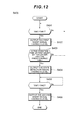
- FIG. 12 is a flowchart for describing an example of the operation of the first shunt circuit, the second shunt circuit, and the control circuit according to one embodiment.
- FIG. 13 is a timing chart for describing the example of the operation of the first shunt circuit, the second shunt circuit, and the control circuit according to one embodiment.
- FIG. 1 to FIG. 13 are drawings for describing an example embodiment.
- FIG. 1 is a block diagram illustrating an integrated circuit 100 according to the example embodiment.
- the integrated circuit 100 is, for example, a semiconductor integrated circuit, such as an IC, made up mainly of semiconductor devices.
- the integrated circuit 100 includes a protected circuit 10 and a protecting circuit 20 .
- the protected circuit 10 is, for example, a main part for realizing the function of the integrated circuit 100 .
- the protected circuit 10 can be configured to include multiple semiconductor devices.
- the protected circuit 10 is connected to an input terminal 11 .
- Supply voltage Vdd is supplied to the protected circuit 10 through the input terminal 11 , and the protected circuit 10 is configured to operate at an operating voltage Vop or less (to be described later) based on the supply voltage Vdd.
- the supply voltage Vdd is supplied to the input terminal 11 .
- the supply voltage Vdd is voltage generated by energy harvesting using natural energy such as photovoltaic, geothermal, or wind power, or renewable energy.
- the value of the supply voltage Vdd depends on the voltage generated by energy harvesting, which can vary with time.
- the supply voltage Vdd of the embodiment corresponds to an example of “input voltage.”
- the protecting circuit 20 is arranged between the input terminal 11 and the protected circuit 10 .
- the protecting circuit 20 is configured to protect the protected circuit 10 from a supply voltage Vdd that is higher than the operating voltage Vop.
- the protecting circuit 20 is configured such that, when a supply voltage Vdd higher than the operating voltage Vop is input from the input terminal 11 , electric current based on the supply voltage Vdd is discharged in order not to apply to the protected circuit 10 the supply voltage Vdd that is higher than or equal to the breakdown voltage Vbd.
- the protecting circuit 20 is configured such that, when a supply voltage Vdd lower than or equal to the operating voltage Vop is input to the input terminal 11 , no electric current is discharged so the supply voltage Vdd is applied directly to the protected circuit 10 .
- the integrated circuit 100 may further include, for example, an input capacitor 12 .
- one end of the input capacitor 12 is connected to a node N 10 between the input terminal 11 and the protecting circuit 20 , and the other end is connected to the ground GND.
- the protecting circuit 20 includes, for example, a first shunt circuit 30 , a second shunt circuit 40 , and a control circuit 50 .
- FIG. 2 is a block diagram illustrating an example of the protecting circuit 20 according to one embodiment.
- the first shunt circuit 30 includes a first shunt pathway 34 connected to the input terminal 11 .
- the first shunt circuit 30 is configured such that electric current dischargeable by the first shunt pathway 34 , i.e., the discharge capacity of the first shunt pathway 34 , is relatively low and the response time is relatively long.
- the first shunt circuit 30 is such that the current dischargeable to the first shunt pathway 34 is about 0.1 mA and the response time is about 50 ⁇ s.
- power consumption when the first shunt circuit 30 operates is about 50 nA.
- the first shunt circuit 30 further includes, for example, a resistor 31 and a resistor 32 , a first comparator 33 , and a first shunt switch 35 .
- the resistor 31 and the resistor 32 are connected in series to each other, and arranged between a node N 11 connected to the input terminal 11 and the ground GND.
- the resistor 31 and the resistor 32 divide the voltage at the node N 11 , i.e., the supply voltage Vdd by division ratios according to respective resistance values to generate divided supply voltage Vdd′ at a node N 12 .
- the divided supply voltage Vdd′ is obtained by dividing the supply voltage Vdd by a predetermined division ratio, the voltage value is only lowered relative to the supply voltage Vdd. Therefore, for example, the time variation of the divided supply voltage Vdd′ is equivalent to the time variation of the supply voltage Vdd.
- the first comparator 33 is configured to drive the first shunt switch 35 based on the divided supply voltage Vdd′.
- the non-inverting input terminal of the first comparator 33 is connected to a node N 13 , at which the voltage is the same as the voltage at the node N 12 , and the voltage Vdd′ divided by the resistor 31 and the resistor 32 is input thereto.
- a predetermined first shunt voltage Vsh 1 is input to the inverting input terminal of the first comparator 33 .
- the supply voltage Vdd is input to the first comparator 33 as the power supply.
- the first comparator 33 When the supply voltage Vdd is higher than or equal to a predetermined value, e.g., higher than or equal to the minimum operating voltage, the first comparator 33 operates, while when the supply voltage Vdd is lower than the predetermined value, the first comparator 33 is deactivated. Usually, since the predetermined value at which the first comparator 33 operates is small enough compared with the value of the supply voltage Vdd input to the input terminal 11 , the first comparator 33 continues to operate while the supply voltage Vdd is input to the input terminal 11 and consumes power.
- a predetermined value e.g., higher than or equal to the minimum operating voltage
- the first comparator 33 compares the divided supply voltage Vdd′ with the first shunt voltage Vsh 1 to output a first shunt signal Ssh 1 based on the comparison result. For example, when the divided supply voltage Vdd′ is higher than the first shunt voltage Vsh 1 , the first comparator 33 outputs the first shunt signal Ssh 1 having a relatively high voltage level (hereinafter called the “H level”). On the other hand, for example, when the divided supply voltage Vdd′ is lower than or equal to the first shunt voltage Vsh 1 , the first comparator 33 outputs the first shunt signal Ssh 1 having a relatively low level (hereinafter called the “L level”).
- H level relatively high voltage level
- L level relatively low level
- the first shunt pathway 34 is configured to be able to discharge electric current based on the supply voltage Vdd.
- the first shunt pathway 34 is, for example, a conductive wire, one end of which is connected to a node N 14 connected to the input terminal 11 and the other end of which is connected to the ground GND.
- the first shunt switch 35 is provided on the first shunt pathway 34 .
- the first shunt switch 35 is, for example, an n-channel metal-oxide semiconductor field-effect transistor (hereinafter called “MOSFET”), whose drain is connected to the node N 14 and source is connected to the ground GND.
- MOSFET metal-oxide semiconductor field-effect transistor
- the first shunt signal Ssh 1 of the first comparator 33 is input to the gate of the first shunt switch 35 .
- the H-level voltage of the first shunt signal Ssh 1 is set to a value larger enough than that of a threshold voltage for the first shunt switch 35 . Therefore, when the first shunt signal Ssh 1 is in the H level, the first shunt switch 35 is turned on, and the first shunt pathway 34 is electrically connected. This leads to discharging of the electric current based on the supply voltage Vdd through the first shunt pathway 34 as the drain current of the first shunt switch 35 . On the other hand, when the first shunt signal Ssh 1 is in the L level, the first shunt switch 35 is turned off, and the first shunt pathway 34 is electrically disconnected.
- the second shunt circuit 40 includes a second shunt pathway 44 connected to the input terminal 11 .
- the second shunt circuit 40 is configured to have an amount of electric current dischargeable by the second shunt pathway 44 , i.e., a relatively high discharge capacity of the second shunt pathway 44 , and a relatively short response time.
- the second shunt circuit 40 is such that the electric current dischargeable into the second shunt pathway 44 is about 100 mA and the response time is about 0.1 ⁇ s.
- power consumption when the second shunt circuit 40 operates is about 10 ⁇ A.
- discharge capacity in this application refers to electric current dischargeable per unit time, i.e., the amount of charge per unit time.
- discharge capacity for example, ampere (A) or joule (J) is used.
- A ampere
- J joule
- the second shunt circuit 40 further includes, for example, a second comparator 43 and a second shunt switch 45 .
- the second comparator 43 is configured to drive the second shunt switch 45 based on the divided supply voltage Vdd′.
- the non-inverting input terminal of the second comparator 43 is connected to the node N 13 of the first shunt circuit 30 , and the divided supply voltage Vdd′ is input thereto. Further, a predetermined second shunt voltage Vsh 2 is input to the inverting input terminal of the second comparator 43 . Further, an enable signal Sen is input from the control circuit 50 (to be described later) to the second comparator 43 as the supply voltage.
- the second comparator 43 When the enable signal Sen is in the H level, the second comparator 43 operates, while when the enable signal Sen is in the L level, the second comparator 43 is deactivated. In other words, when the enable signal Sen is in the H level, the second comparator 43 consumes power, while when the enable signal Sen is in the L level, the second comparator 43 consumes no power.
- the second comparator 43 compares the divided supply voltage Vdd′ with the second shunt voltage Vsh 2 , and outputs a second shunt signal Ssh 2 based on the comparison result. For example, when the divided supply voltage Vdd′ is higher than the second shunt voltage Vsh 2 , the second comparator 43 outputs the second shunt signal Ssh 2 having the H level. On the other hand, for example, when the divided supply voltage Vdd′ is lower than or equal to the second shunt voltage Vsh 2 , the second comparator 43 outputs the second shunt signal Ssh 2 having the L level.
- the second shunt pathway 44 is configured to be able to discharge electric current based on the supply voltage Vdd.
- the second shunt pathway 44 is, for example, a conductive wire, one end of which is connected to a node N 21 connected to the input terminal 11 and the other end of which is connected to the ground GND.
- the second shunt switch 45 is provided on the second shunt pathway 44 .
- the second shunt switch 45 is, for example, an n-channel MOSFET whose drain is connected to the node N 21 and source is connected to the ground GND.
- the second shunt signal Ssh 2 of the second comparator 43 is input to the gate of the second shunt switch 45 .
- the H-level voltage of the second shunt signal Ssh 2 is set to a value larger enough than that of a threshold voltage for the second shunt switch 45 . Therefore, when the second shunt signal Ssh 2 is in the H level, the second shunt switch 45 is turned on, and the second shunt pathway 44 is electrically connected. This leads to discharging of the electric current based on the supply voltage Vdd through the second shunt pathway 44 as the drain current of the second shunt switch 45 . On the other hand, when the second shunt signal Ssh 2 is in the L level, the second shunt switch 45 is turned off, and the second shunt pathway 44 is electrically disconnected.
- the control circuit 50 is configured to control the second shunt circuit 40 .
- the control circuit 50 includes, for example, an input voltage variation detector 60 , a first shunt circuit state detector 80 , and an OR circuit 51 .
- the input voltage variation detector 60 is configured to enable the second shunt pathway 44 to discharge based on the time variation of the supply voltage Vdd. More specifically, the input voltage variation detector 60 is configured to activate the second comparator 43 in the second shunt circuit 40 based on the time variation of the supply voltage Vdd.
- the input voltage variation detector 60 is connected to a node N 31 connected to the input terminal 11 , and the supply voltage Vdd is input thereto.
- the input voltage variation detector 60 is configured to detect the time variation of the supply voltage Vdd, and output a variation detection signal Svd based on the detection result.
- the first shunt circuit state detector 80 is configured to enable the second shunt pathway 44 to discharge based on the time required to discharge the electric current based on the supply voltage Vdd into the first shunt pathway 34 , i.e., the operating time of the first shunt switch 35 .
- the first shunt circuit state detector 80 is connected to a node N 15 in the first shunt circuit 30 , and the first shunt signal Ssh 1 of the first comparator 33 is input thereto.
- the first shunt circuit state detector 80 is configured to detect the operating time of the first shunt switch 35 , and output a state detection signal Ssd based on the detection result.
- the variation detection signal Svd of the input voltage variation detector 60 , and the state detection signal Ssd of the first shunt circuit state detector 80 are input to the OR circuit 51 .
- the OR circuit 51 performs an OR operation on the variation detection signal Svd and the state detection signal Ssd to output the enable signal Sen mentioned above.
- the enable signal Sen becomes the L level when both the variation detection signal Svd and the state detection signal Ssd are in the L level, or the H level when at least either of the variation detection signal Svd and the state detection signal Ssd is in the H level.
- the control circuit 50 thus configured consumes little power.
- the power consumption of the control circuit 50 is about 3 nA. Therefore, the power consumption of the first shunt circuit 30 and the second shunt circuit 40 accounts for most of the power consumption in the protecting circuit 20 .
- the amount of electric current dischargeable per predetermined time, e.g., the discharge capacity, and the response time in a shunt circuit provided in the protecting circuit have a trade-off relationship with the power consumption.
- a shunt circuit having a relatively high discharge capacity and a relatively short response time tends to consume more power.
- a shunt circuit consuming less power tends to have a low discharge capacity and a long response time. Therefore, in conventional protecting circuits, the discharge capacity, the response time, and the power consumption of a shunt circuit are set to be adequate for the intended use and purpose.
- FIG. 3 is a graph representing an example of a relationship between illuminance in electric power generation by light energy and electric generating capacity.
- the light energy greatly increases the illuminance scale depending on the type of light, and the electric generating capacity of the light energy tends to become very high.
- the electric generating capacity is about 2 ⁇ W/cm 2 (e.g., 2 ⁇ W of power generated by a photovoltaic electric source with an area of 1 cm 2 ).
- the illuminance is about 20000 1 ⁇
- the electric generating capacity is about 30 mW/cm 2 .
- the protecting circuit 20 includes the first shunt circuit 30 including the first shunt pathway 34 connected to the input terminal 11 and configured to have a relatively low discharge capacity of the first shunt pathway 34 and a relatively long response time. Therefore, for example, when indoor light is incident on the photovoltaic electric source to generate supply voltage Vdd having a low voltage value, the first shunt circuit 30 operates to enable the discharge of part of electric current based on the supply voltage Vdd into the first shunt pathway 34 . At this time, the first shunt circuit 30 continues to operate during the input of the supply voltage Vdd, but the power consumption thereof is low.
- the protecting circuit 20 includes: the second shunt circuit 40 including the second shunt pathway 44 connected to the input terminal 11 and configured to have a relatively high discharge capacity of the second shunt pathway 44 and a relatively short response time; and the control circuit 50 configured to enable the second shunt pathway 44 to discharge based on the time variation of supply voltage Vdd input to the input terminal 11 . Therefore, for example, when sunlight suddenly enters the photovoltaic electric source on which the indoor light was incident to generate supply voltage Vdd having a high voltage value, since the time variation of the supply voltage Vdd becomes large, the control circuit 50 can discharge high electric current into the second shunt pathway 44 at high speed based on the time variation of this supply voltage Vdd. Although the power consumption of the second shunt circuit 40 is high, the control circuit 50 can activate the second shunt circuit 40 when the time variation of the supply voltage Vdd is large in order to suppress the power consumption of the second shunt circuit 40 .
- control circuit 50 can operate when the supply voltage Vdd is lower than or equal to the minimum operating voltage Vmin (to be described later).
- the first case is a case where a supply voltage Vdd input to the input terminal 11 is higher than or equal to the operating voltage Vop of the protected circuit 10 , and the time variation of the supply voltage Vdd is smaller than or equal to a predetermined variation, e.g., where a rise in supply voltage Vdd per unit time is smaller than or equal to a first value.
- FIG. 4 is a flowchart for describing an example of the operation of the first shunt circuit 30 according to the embodiment. For example, when supply voltage Vdd is input to the input terminal 11 , the first shunt circuit 30 starts a first shunt process S 100 illustrated in FIG. 4 .
- the first comparator 33 first determines whether the divided supply voltage Vdd′ is higher than the first shunt voltage Vsh 1 (Vdd′>Vsh 1 ) (S 101 ).
- the first comparator 33 repeats step S 101 until the divided supply voltage Vdd′ exceeds the first shunt voltage Vsh 1 . While the divided supply voltage Vdd′ is lower than or equal to the first shunt voltage Vsh 1 , since the first comparator 33 outputs the first shunt signal Ssh 1 having the L level, the first shunt switch 35 is off.
- the first comparator 33 outputs the first shunt signal Ssh 1 having the H level (S 102 ). This results in turning on the first shunt switch 35 to discharge electric current into the first shunt pathway 34 .
- step S 102 the first shunt circuit 30 completes the first shunt process S 100 .
- FIG. 5 is a timing chart for describing the example of the operation of the first shunt circuit 30 according to the embodiment.
- the horizontal axis represents time
- the vertical axis represents voltage with the supply voltage Vdd indicated by the solid line and the divided supply voltage Vdd′ indicated by the dot-and-dash line.
- a state where each part of the protecting circuit 20 consumes power is expressed as “the operation is on” and a state where each part of the protecting circuit 20 consumes no power is expressed as “the operation is off.” As illustrated in FIG.
- the first shunt switch 35 when the supply voltage Vdd is higher than or equal to the operating voltage Vop, and the divided supply voltage Vdd′ exceeds the first shunt voltage Vsh 1 at time t 101 as a result of a gradual increase in the supply voltage Vdd and the divided supply voltage Vdd′, the first shunt switch 35 is turned on to pass electric current through the first shunt pathway 34 in order to enable the discharge of the electric current.
- the first shunt switch 35 is turned on at timing of time t 102 after a predetermined time has elapsed from time t 101 .
- the first shunt switch 35 is turned off to stop discharging through the first shunt pathway 34 .
- the first shunt switch 35 is turned off at timing of time t 103 after a predetermined time has elapsed since the divided supply voltage Vdd′ became lower than or equal to the first shunt voltage Vsh 1 .
- the variation detection signal Svd of the input voltage variation detector 60 is in the L level. Further, since the operating time of the first shunt switch 35 is short, the state detection signal Ssd of the first shunt circuit state detector 80 is also in the L level. As a result, the operation of the second comparator 43 in the second shunt circuit 40 is off, and the second shunt signal Ssh 2 of the second comparator 43 is in the L level.
- FIG. 4 illustrates an example in which the first shunt circuit 30 completes the first shunt process S 100 after step S 102 , but this is merely a non-limiting example.
- the first shunt circuit 30 may repeat steps S 101 and S 102 before completing the first shunt process S 100 .
- FIG. 6 is a circuit diagram illustrating an example of the input voltage variation detector 60 according to an example embodiment.
- the input voltage variation detector 60 includes, for example, a switch 61 a and a switch 61 b , a resistor 62 a and a resistor 62 b , a detection capacitor 63 , transistors 64 a to 64 f , a capacitor 65 , an OR circuit 66 , an inverter 67 , a delay circuit 68 , and an inverter 69 .
- One end of the switch 61 a is connected to a node N 41 , and the other end is connected to a node N 42 .
- the second shunt voltage Vsh 2 is input to the node N 41 .
- a delay signal Svdd (to be described later) is input to the switch 61 a , and the switch 61 a electrically connects or disconnects the node N 41 and the node N 42 based on the delay signal Svdd.
- One end of the switch 61 b is connected to a node N 43 , and the other end is connected to the node N 42 .
- the supply voltage Vdd is input to the node N 43 .
- an exclusive delay signal Sxvdd (to be described later) is input to the switch 61 b , and the switch 61 b electrically connects or disconnects the node N 43 and the node N 42 based on the exclusive delay signal Sxvdd.
- the resistor 62 a is a so-called pull-up resistor to bring the voltage at the node N 45 to the H level when both the transistor 64 b and the transistor 64 e (to be described later) are off.
- the resistor 62 b is a so-called pull-up resistor to bring the voltage at the node N 47 to the H level when both the transistor 64 c and the transistor 64 f (to be described later) are off.
- One end of the detection capacitor 63 is connected to the node N 42 , and the other end is connected to a node N 48 .
- the second shunt voltage Vsh 2 or the supply voltage Vdd is applied between the node N 42 and the ground GND by the switching actions of the switch 61 a and the switch 61 b .
- the detection capacitor 63 accumulates electric charge by the second shunt voltage Vsh 2 or the supply voltage Vdd.
- the transistor 64 a and the transistor 64 d are connected in series between the node N 48 and the ground GND.
- the transistor 64 a is, for example, an n-channel MOSFET with the drain and gate connected to a node N 49 and the source connected to the ground GND.
- the transistor 64 d is, for example, an n-channel MOSFET with the drain and gate connected to the node N 48 and the source connected to the node N 49 .
- the transistor 64 b and the transistor 64 e are connected in series between the node N 45 and the ground GND.
- the transistor 64 b is, for example, an n-channel MOSFET with the gate connected to the node N 49 and the source connected to the ground GND.
- the transistor 64 e is, for example, an n-channel MOSFET with the gate connected to the node N 48 and the drain connected to the node N 45 . Further, the drain of the transistor 64 b and the source of the transistor 64 e are connected to each other.
- the transistor 64 c and the transistor 64 f are connected in series between the node N 47 and the ground GND.
- the transistor 64 c is, for example, an n-channel MOSFET with the gate connected to the node N 49 and the source connected to the ground GND.
- the transistor 64 f is, for example, an n-channel MOSFET with the gate connected to the node N 48 and the drain connected to the node N 47 . Further, the drain of the transistor 64 c and the source of the transistor 64 f are connected to each other.
- the transistors 64 a to 64 f thus connected act as a current mirror, particularly as a cascode current mirror.
- the transistor 64 a and the transistor 64 d are turned on to pass electric current through
- the transistor 64 b and the transistor 64 e and the transistor 64 c and the transistor 64 f are all turned on.
- the electric current flowing through the transistor 64 b and the transistor 64 e and the electric current flowing through the transistor 64 c and the transistor 64 f are the same or nearly the same as the electric current flowing through the transistor 64 a and the transistor 64 d due to the action of the current mirror.
- the electric charge accumulated in the detection capacitor 63 can flow into the transistor 64 a and the transistor 64 d as electric current of a mirror source of the current mirror. Since this current value is determined by the impedance of the detection capacitor 63 , a value such as the capacity or frequency of the detection capacitor 63 can be set as the current value to determine electric current flowing through the transistor 64 a and the transistor 64 d.
- the supply voltage Vdd is applied between the node N 42 and the ground GND.
- the supply voltage Vdd is higher than or equal to a total value of threshold voltages for the transistor 64 a and the transistor 64 d .
- the input voltage variation detector 60 consumes no power without operating. Therefore, the total value of threshold voltages for the transistor 64 a and the transistor 64 d corresponds to the minimum operating voltage Vmin (to be described later).
- One end of the capacitor 65 is connected to a node N 50 having the same electric potential as the node N 47 , and the other end is connected to the ground GND. Therefore, the capacitor 65 accumulates electric charge while the node N 47 is in the H level. On the other hand, when the node N 47 becomes the L level, the capacitor 65 discharges the accumulated electric charge.
- the node N 47 and the node N 50 can maintain the H level until a predetermined time has elapsed since the node N 45 was changed to the L level due to the discharging of the capacitor 65 .
- the voltage at the node N 45 and the voltage at the node N 50 are input to the OR circuit 66 .
- the OR circuit 66 performs an OR operation on the voltage at the node N 45 and the voltage at the node N 50 to output a signal 51 .
- the signal 51 becomes the L level
- the signal 51 becomes the H level
- the signal S 1 of the OR circuit 66 is input to the inverter 67 .
- the inverter 67 inverts the level of the signal S 1 and outputs the inverted signal as the variation detection signal Svd mentioned above.
- the variation detection signal Svd of the inverter 67 is input to the delay circuit 68 .
- the delay circuit delays this variation detection signal Svd for a predetermined time, and outputs it as the delay signal Svdd mentioned above.
- the delay signal Svdd of the delay circuit 68 is input to the inverter 69 .
- the inverter 69 inverts the level of the delay signal Svdd and outputs the inverted signal as the exclusive delay signal Sxvdd mentioned above.
- the second case is a case where the supply voltage Vdd input to the input terminal 11 is higher than or equal to the minimum operating voltage Vmin of the input voltage variation detector 60 , and the time variation of the supply voltage Vdd is larger than a predetermined variation, e.g., the rise in the supply voltage Vdd per unit time is greater than the first value.
- FIG. 7 is a flowchart for describing a first example of the operation of the second shunt circuit 40 and the control circuit 50 according to one embodiment.
- the control circuit 50 starts a single second shunt process S 200 illustrated in FIG. 7 .
- the switch 61 a illustrated in FIG. 6 is off and the switch 61 b illustrated in FIG. 6 is on.
- the input voltage variation detector 60 first determines whether the supply voltage Vdd is higher than the minimum operating voltage Vmin (Vdd>Vmin) (S 201 ).
- the input voltage variation detector 60 repeats step S 201 until the supply voltage Vdd becomes higher than the minimum operating voltage Vmin. While the supply voltage Vdd is lower than or equal to the minimum operating voltage Vmin, since both the node N 45 and the node N 47 are in the H level due to the pull-up actions of the resistor 62 a and the resistor 62 b illustrated in FIG. 6 , both variation detection signals Svd are in the L level. At this time, since the state detection signal Ssd illustrated in FIG. 2 is also in the L level, the enable signal Sen of the OR circuit 51 is in the L level. As a result, the second comparator 43 does not operate, and the second shunt switch 45 is off.
- the input voltage variation detector 60 determines whether the rise in the supply voltage Vdd per unit time, e.g., a slope of the supply voltage Vdd as a time-series signal, is greater than the first value (S 202 ).
- the input voltage variation detector 60 repeats steps S 201 and S 202 until the slope of the supply voltage Vdd becomes greater than the predetermined value. While the slope of the supply voltage Vdd is smaller than or equal to the first value, since both the transistor 64 a and the transistor 64 d illustrated in FIG. 6 are off and no electric current flows into the mirror source of the current mirror, both the node N 45 and the node N 47 remain in the H level due to the pull-up actions of the resistor 62 a and the resistor 62 b , and the variation detection signal Svd is in the L level. Further, since the state detection signal Ssd illustrated in FIG. 2 is also in the L level, the enable signal Sen of the OR circuit 51 is in the L level.
- the second comparator 43 does not operate, and the second shunt switch 45 is off.
- the second shunt circuit 40 consumes no power until the supply voltage Vdd becomes higher than the minimum operating voltage Vmin and the slope of the supply voltage Vdd becomes greater than the first value.
- the input voltage variation detector 60 outputs the variation detection signal Svd having the H level (S 203 ).
- the enable signal Sen of the OR circuit 51 illustrated in FIG. 2 is changed from the L level to the H level, and the second comparator 43 in the second shunt circuit 40 is activated.
- the second comparator 43 determines whether the divided supply voltage Vdd′ is higher than the second shunt voltage Vsh 2 (Vdd′>Vsh 2 ) (S 204 ).
- the second comparator 43 repeats step S 204 until the divided supply voltage Vdd′ becomes higher than the second shunt voltage Vsh 2 . Since the second comparator 43 outputs the second shunt signal Ssh 2 having the L level while the divided supply voltage Vdd′ is lower than or equal to the second shunt voltage Vsh 2 , the second shunt switch 45 is off.
- step S 205 the second shunt circuit 40 and the control circuit 50 complete the single second shunt process S 200 .
- FIG. 8 is a timing chart for describing the first example of the operation of the second shunt circuit 40 and the control circuit 50 according to the embodiment.
- the horizontal axis represents time
- the vertical axis represents voltage with the supply voltage Vdd indicated by the solid line and the divided supply voltage Vdd′ indicated by the dot-and-dash line.
- the supply voltage Vdd exceeds the minimum operating voltage Vmin at time t 201 as a result of a sharp rise in the supply voltage Vdd and the divided supply voltage Vdd′, the operation of the input voltage variation detector 60 is turned on.
- the variation detection signal Svd is changed from the L level to the H level a little later than time t 201 by the electric charge accumulated in the capacitor 65 illustrated in FIG. 6 to turn on the operation of the second comparator 43 illustrated in FIG. 2 .
- the second shunt signal Ssh 2 of the second comparator 43 becomes the H level.
- the second shunt signal Ssh 2 is changed from the L level to the H level at timing after a predetermined time has elapsed from time t 202 .
- the second shunt switch 45 is turned on.
- the second shunt switch 45 is changed from off to on at timing after a predetermined time has elapsed from time t 203 .
- high electric current flows into the second shunt pathway 44 at time t 204 to decrease the supply voltage Vdd and the divided supply voltage Vdd′ rapidly.
- the second shunt signal Ssh 2 of the second comparator 43 becomes the L level.
- the second shunt signal Ssh 2 is changed from the H level to the L level at timing after a predetermined time has elapsed from time t 205 .
- the second shunt switch 45 is turned off at time t 206 to stop the drop in the supply voltage Vdd and the divided supply voltage Vdd′.
- the input voltage variation detector 60 illustrated in FIG. 6 detects that the rise in the supply voltage Vdd per unit time becomes smaller than or equal to the first value at time t 204 .
- the electric charge accumulated in the detection capacitor 63 continues to pass electric current through the transistor 64 a and the transistor 64 d , the node N 45 , the node N 47 , and the node N 50 all maintain the L level. Therefore, the variation detection signal Svd maintains the H level for a period of time corresponding to the amount of electric charge accumulated in the detection capacitor 63 after time t 204 , and becomes the L level, for example, after time t 206 .
- the operation of the input voltage variation detector 60 and the second comparator 43 illustrated in FIG. 2 is turned off.
- the second comparator 43 may be so preset that the second shunt signal Ssh 2 will become the L level when the enable signal Sen of the OR circuit 51 illustrated in FIG. 2 is in the L level.
- the first shunt circuit 30 illustrated in FIG. 2 since the supply voltage Vdd is input to the input terminal 11 , the operation of the first comparator 33 is on. However, since the response time of the first shunt circuit 30 is very long compared with the response time of the second shunt circuit 40 , the first shunt circuit 30 cannot follow the sharp rise in the supply voltage Vdd and the divided supply voltage Vdd′. Therefore, even when the divided supply voltage Vdd′ is higher than the first shunt signal Vsh 1 , the first shunt signal Ssh 1 of the first comparator 33 remains in the L level. Then, since the first shunt circuit state detector 80 detects the operating time of the first shunt switch 35 , the state detection signal Ssd of the first shunt circuit state detector 80 is in the L level.
- the third case is a case where the supply voltage Vdd input to the input terminal 11 is higher than or equal to the minimum operating voltage Vmin of the input voltage variation detector 60 , the rise in the supply voltage Vdd per unit time is greater than the first value, and further the supply voltage Vdd cannot be sufficiently decreased by one discharge by the second shunt circuit 40 .
- FIG. 9 is a flowchart for describing a second example of the operation of the second shunt circuit 40 and the control circuit 50 according to one embodiment.
- the control circuit 50 starts a multiple second shunt process S 300 illustrated in FIG. 9 .
- the switch 61 a illustrated in FIG. 6 is off and the switch 61 b illustrated in FIG. 6 is on.
- steps S 301 to S 305 in the multiple second shunt process S 300 are the same as the steps S 201 to S 205 in the single second shunt process S 200 illustrated in FIG. 7 , the description thereof will be omitted.
- the input voltage variation detector 60 determines whether the rise in the supply voltage Vdd per unit time, e.g., the slope of the supply voltage Vdd as a time-series signal, is greater than a second value (S 306 ).
- the second value is a value smaller than the first value mentioned above.
- the input voltage variation detector 60 uses the delay signal Svdd and the exclusive delay signal Sxvdd illustrated in FIG. 6 to switch between on and off of the switches 61 a and 61 b in order to charge the detection capacitor 63 at the second shunt voltage Vsh 2 .
- the input voltage variation detector 60 uses delay signal Svdd and the exclusive delay signal Sxvdd to switch between on and off of the switches 61 a and 61 b again to charge the detection capacitor 63 at the supply voltage Vdd.
- the slope of a voltage difference between the supply voltage Vdd and the second shunt voltage Vsh 2 is detected. Detecting the slope of a voltage difference between the supply voltage Vdd and the second shunt voltage Vsh 2 means that the slope of the supply voltage Vdd is greater than the second value.
- step S 306 is executed after step S 305 is illustrated, but this is merely a non-limiting example. Since steps S 304 and S 305 are executed by the second shunt circuit 40 and step S 306 is executed by the control circuit 50 , the second shunt circuit 40 and the control circuit 50 can execute steps S 304 and S 305 , and step S 306 in parallel, for example.
- FIG. 10 is a timing chart for describing the second example of the operation of the second shunt circuit 40 and the control circuit 50 according to one embodiment.
- the horizontal axis represents time
- the vertical axis represents voltage with the supply voltage Vdd indicated by the solid line and the divided supply voltage Vdd′ indicated by the dot-and-dash line.
- the delay signal Svdd becomes the H level and the exclusive delay signal Sxvdd becomes the L level at time t 306 to turn on and off the switch 61 a and the switch 61 b illustrated in FIG. 6 , respectively.
- the second shunt voltage Vsh 2 is applied to the detection capacitor 63 illustrated in FIG. 6 .
- the delay signal Svdd becomes the L level and the exclusive delay signal Sxvdd becomes the H level at time t 307 to turn off and on the switch 61 a and the switch 61 b illustrated in FIG. 6 , respectively.
- the supply voltage Vdd is applied again to the detection capacitor 63 illustrated in FIG. 6 .
- the second shunt switch 45 is turned on.
- the second shunt switch 45 is changed from off to on at timing after a predetermined time has elapsed from time t 308 .
- high electric current flows into the second shunt pathway 44 again at time t 309 to decrease the supply voltage Vdd and the divided supply voltage Vdd′ rapidly.
- the second shunt signal Ssh 2 becomes the L level.
- the second shunt signal Ssh 2 is changed from the H level to the L level at timing after a predetermined time has elapsed since the divided supply voltage Vdd′ fell below the second shunt voltage Vsh 2 .
- the second shunt switch 45 is turned off at time t 310 to stop the drop in the supply voltage Vdd and the divided supply voltage Vdd′.
- the input voltage variation detector 60 illustrated in FIG. 6 detects that the rise in the supply voltage Vdd per unit time becomes smaller than or equal to the first value and the voltage variation becomes smaller than or equal to a predetermined value at time t 309 .
- the electric charge accumulated in the detection capacitor 63 continues to pass electric current through the transistor 64 a and the transistor 64 d , the node N 45 , the node N 47 , and the node N 50 all maintain the L level. Therefore, the variation detection signal Svd maintains the H level for a period of time corresponding to the amount of electric charge accumulated in the detection capacitor 63 after time t 309 , and becomes the L level, for example, after time t 310 .
- the operation of the input voltage variation detector 60 and the second comparator 43 illustrated in FIG. 2 is turned off.
- the second comparator 43 may be so preset that the second shunt signal Ssh 2 will become the L level when the enable signal Sen of the OR circuit 51 illustrated in FIG. 2 is in the L level.
- the first shunt circuit 30 illustrated in FIG. 2 since the supply voltage Vdd is input to the input terminal 11 , the operation of the first comparator 33 is on. However, since the response time of the first shunt circuit 30 is very long compared with the response time of the second shunt circuit 40 , the first shunt circuit 30 cannot follow the sharp rise in the supply voltage Vdd and the divided supply voltage Vdd′. Therefore, even when the divided supply voltage Vdd′ is higher than the first shunt signal Vsh 1 , the first shunt signal Ssh 1 of the first comparator 33 remains in the L level. Then, since the first shunt circuit state detector 80 detects the operating time of the first shunt switch 35 , the state detection signal Ssd of the first shunt circuit state detector 80 is in the L level.
- FIG. 11 is a circuit diagram illustrating an example of the first shunt circuit state detector 80 according to the embodiment. As illustrated in FIG. 11 , the first shunt circuit state detector 80 includes, for example, a resistor 81 , a capacitor 82 , and an AND circuit 83 .
- One end of the resistor 81 is connected to a node N 61 to which the first shunt signal Ssh 1 of the first shunt circuit 30 illustrated in FIG. 2 is input, and the other end is connected to a node N 62 .
- One end of the capacitor 82 is connected to the node 62 , and the other end is connected to the ground GND.
- the resistor 81 and the capacitor 82 thus connected constitute an RC circuit to set a time constant determined by the resistance value of the resistor 81 and the capacitance of the capacitor 82 in order to generate a delay signal Sshd for delaying the first shunt signal Ssh 1 by a predetermined time.
- the first shunt signal Ssh 1 of the first shunt circuit 30 and the delay signal Sshd of the resistor 81 and the capacitor 82 are input to the AND circuit 83 .
- the AND circuit 83 performs an AND operation on the first shunt signal Ssh 1 and the delay signal Sshd to output the state detection signal Ssd mentioned above.
- the state detection signal Ssd becomes the H level
- the state detection signal Ssd becomes the L level.
- the fourth case is a case where the supply voltage Vdd input to the input terminal 11 is higher than or equal to the operating voltage Vop of the protected circuit 10 , the rise in the supply voltage Vdd per unit time is smaller than or equal to the first value, and further the supply voltage Vdd cannot be sufficiently decreased by discharging through the first shunt circuit 30 .
- FIG. 12 is a flowchart for describing an example of the operation of the first shunt circuit 30 , the second shunt circuit 40 , and the control circuit 50 according to one embodiment.
- the second shunt circuit 40 and the control circuit 50 start a first-and-second shunt process S 400 illustrated in FIG. 12 .
- the switch 61 a illustrated in FIG. 6 is off and the switch 61 b illustrated in FIG. 6 is on.
- steps S 401 and S 402 in the first-and-second shunt process S 400 are the same as the steps S 101 and S 102 in the first shunt process S 100 illustrated in FIG. 4 , the description thereof will be omitted.
- the first shunt circuit state detector 80 determines whether the operating time of the first shunt switch 35 is longer than a predetermined time (S 403 ).
- the first shunt circuit 30 repeats steps S 401 to S 403 .
- the first shunt circuit state detector 80 outputs the state detection signal Ssd having the H level (S 404 ).
- the enable signal Sen of the OR circuit 51 illustrated in FIG. 2 is changed from the L level to the H level, and the second comparator 43 in the second shunt circuit 40 is activated.
- steps S 405 and S 406 in the first-and-second shunt process S 400 are the same as the steps S 204 and S 205 in the second shunt process S 200 illustrated in FIG. 7 , the description thereof will be omitted.
- step S 406 the first shunt circuit 30 , the second shunt circuit 40 , and the control circuit 50 complete the first-and-second shunt process S 400 .
- FIG. 13 is a timing chart for describing the example of the operation of the first shunt circuit 30 , the second shunt circuit 40 , and the control circuit 50 according to one embodiment.
- the horizontal axis represents time
- the vertical axis represents voltage with the supply voltage Vdd indicated by the solid line and the divided supply voltage Vdd′ indicated by the dot-and-dash line.
- the state detection signal Ssd is changed from the L level to the H level at time t 403 to turn on the operation of the second comparator 43 in the second shunt circuit 40 .
- the second shunt signal Ssh 2 becomes the H level.
- the second shunt signal Ssh 2 is changed from the L level to the H level at timing after a predetermined time has elapsed from time t 403 .
- the second shunt switch 45 is turned on.
- the second shunt switch 45 is changed from off to on at timing after a predetermined time has elapsed since the second shunt signal Ssh 2 became the H level. As a result, high electric current flows into the second shunt pathway 44 at time t 404 .
- the operation of the second shunt circuit 40 is turned off.
- the second shunt signal Ssh 2 becomes the L level
- the second shunt switch 45 is turned off, and the drop in the supply voltage Vdd and the divided supply voltage Vdd′ is stopped.
- the first shunt signal Ssh 1 becomes the L level.
- the first shunt signal Ssh 1 is changed from the H level to the L level at timing after a predetermined time has elapsed since the divided supply voltage Vdd′ fell below the first shunt voltage Vsh 1 .
- the first shunt switch 35 is turned off after time t 405 .
- the variation detection signal Svd of the input voltage variation detector 60 illustrated in FIG. 6 is in the L level.
- the delay signal Svdd is in the L level, and the exclusive delay signal Sxvdd is in the H level.
- FIG. 13 illustrates an example in which the first shunt voltage Vsh 1 and the second shunt voltage Vsh 2 have the same value, but this is merely a non-limiting example.
- the first shunt voltage Vsh 1 and the second shunt voltage Vsh 2 may have different values.
- the first shunt circuit 30 including the first shunt pathway 34 connected to the input terminal 11 and configured to have a relatively low discharge capacity of the first shunt pathway 34 and a relatively long response time is provided. Therefore, for example, when indoor light enters a photovoltaic electric source to generate supply voltage Vdd having a low voltage value, the first shunt circuit 30 operates to enable discharge electric current based on the input voltage Vdd into the first shunt pathway 34 . At this time, although the first shunt circuit 30 continues to operate while the supply voltage Vdd is input, the power consumption is low.
- the protecting circuit 20 and the integrated circuit 100 further includes: the second shunt circuit 40 including the second shunt pathway 44 connected to the input terminal 11 and configured to have a relatively high discharge capacity of the second shunt pathway 44 and a relatively short response time; and the control circuit 50 configured to enable the second shunt pathway 44 to discharge based on a time variation of supply voltage Vdd input to the input terminal 11 . Therefore, for example, when sunlight suddenly enters the photovoltaic electric source on which indoor light was incident to generate supply voltage Vdd having a high voltage value, since the time variation of the supply voltage Vdd becomes great, the control circuit 50 can discharge high electric current into the second shunt pathway 44 at high speed based on the time variation of this supply voltage Vdd.
- the control circuit 50 can operate the second shunt circuit 40 only when the time variation of the supply voltage Vdd is great, and this can suppress the power consumption of the second shunt circuit 40 . Therefore, the protected circuit 10 can be protected by discharging electric current sufficient for supply voltage Vdd having a large time variation while suppressing power consumption when the time variation of the supply voltage Vdd is small.
- Coupled may mean connected directly or connected indirectly through one or more intervening components.
Landscapes
- Electronic Switches (AREA)
- Measurement Of Current Or Voltage (AREA)
Abstract
Description
Claims (20)
Priority Applications (2)
| Application Number | Priority Date | Filing Date | Title |
|---|---|---|---|
| US15/082,882 US9614366B2 (en) | 2015-05-15 | 2016-03-28 | Protecting circuit and integrated circuit |
| PCT/US2016/024651 WO2016186734A1 (en) | 2015-05-15 | 2016-03-29 | Protecting circuit and integrated circuit |
Applications Claiming Priority (2)
| Application Number | Priority Date | Filing Date | Title |
|---|---|---|---|
| US201562162485P | 2015-05-15 | 2015-05-15 | |
| US15/082,882 US9614366B2 (en) | 2015-05-15 | 2016-03-28 | Protecting circuit and integrated circuit |
Publications (2)
| Publication Number | Publication Date |
|---|---|
| US20160336738A1 US20160336738A1 (en) | 2016-11-17 |
| US9614366B2 true US9614366B2 (en) | 2017-04-04 |
Family
ID=57276208
Family Applications (1)
| Application Number | Title | Priority Date | Filing Date |
|---|---|---|---|
| US15/082,882 Active US9614366B2 (en) | 2015-05-15 | 2016-03-28 | Protecting circuit and integrated circuit |
Country Status (2)
| Country | Link |
|---|---|
| US (1) | US9614366B2 (en) |
| WO (1) | WO2016186734A1 (en) |
Families Citing this family (2)
| Publication number | Priority date | Publication date | Assignee | Title |
|---|---|---|---|---|
| CN107528450B (en) * | 2017-08-29 | 2024-09-06 | 深圳市稳先微电子有限公司 | Voltage comparator, control chip and switching power supply |
| CN115603298A (en) * | 2022-09-30 | 2023-01-13 | 成都芯海创芯科技有限公司(Cn) | Power-on overshoot prevention circuit, chip and electronic equipment |
Citations (14)
| Publication number | Priority date | Publication date | Assignee | Title |
|---|---|---|---|---|
| US6040733A (en) | 1995-08-07 | 2000-03-21 | Micron Technology, Inc. | Two-stage fusible electrostatic discharge protection circuit |
| US6140928A (en) | 1997-10-31 | 2000-10-31 | Toshiba Battery Co., Ltd. | Remaining battery capacity measuring device |
| US6775112B1 (en) | 2000-05-12 | 2004-08-10 | National Semiconductor Corporation | Apparatus and method for improving ESD and transient immunity in shunt regulators |
| US20070285854A1 (en) * | 2006-06-08 | 2007-12-13 | Cypress Semiconductor Corp. | Programmable Electrostatic Discharge (ESD) Protection Device |
| US7518846B1 (en) * | 2006-02-23 | 2009-04-14 | Maxim Integrated Products, Inc. | ESD protection method for low-breakdown integrated circuit |
| US7777996B2 (en) | 2005-06-30 | 2010-08-17 | Lsi Corporation | Circuit protection system |
| US20100277841A1 (en) | 2007-06-07 | 2010-11-04 | Atmel Corporation | Threshold voltage method and apparatus for esd protection |
| US20120016832A1 (en) | 2010-07-14 | 2012-01-19 | Jean-Jacques Berard | Automated document separation |
| US8102632B2 (en) | 2009-03-18 | 2012-01-24 | Advanced Micro Devices, Inc. | Electrostatic discharge power clamp trigger circuit using low stress voltage devices |
| US8605404B2 (en) | 2008-06-06 | 2013-12-10 | Chang Gung University | Cascade electromagnetic pulse protection circuit for high frequency application |
| US8648578B2 (en) | 2007-09-30 | 2014-02-11 | Nxp, B.V. | Capless low drop-out voltage regulator having discharge circuit compensating for on-chip output capacitance and response time |
| US20150236503A1 (en) | 2014-02-14 | 2015-08-20 | Peng Zhu | Electro-static discharge filtering circuit and method, reset circuit, and electronic device |
| US20150288173A1 (en) | 2014-04-02 | 2015-10-08 | Semiconductor Manufacturing International (Shanghai) Corporation | Electrostatic discharge protection circuit and configuration method |
| JP2016056716A (en) | 2014-09-08 | 2016-04-21 | 株式会社神戸製鋼所 | Energy recovery device and ship, and installation method of energy recovery device |
Family Cites Families (1)
| Publication number | Priority date | Publication date | Assignee | Title |
|---|---|---|---|---|
| US20120162832A1 (en) * | 2010-12-27 | 2012-06-28 | Global Unichip Corp. | Esd protection circuit for multi-powered integrated circuit |
-
2016
- 2016-03-28 US US15/082,882 patent/US9614366B2/en active Active
- 2016-03-29 WO PCT/US2016/024651 patent/WO2016186734A1/en not_active Ceased
Patent Citations (14)
| Publication number | Priority date | Publication date | Assignee | Title |
|---|---|---|---|---|
| US6040733A (en) | 1995-08-07 | 2000-03-21 | Micron Technology, Inc. | Two-stage fusible electrostatic discharge protection circuit |
| US6140928A (en) | 1997-10-31 | 2000-10-31 | Toshiba Battery Co., Ltd. | Remaining battery capacity measuring device |
| US6775112B1 (en) | 2000-05-12 | 2004-08-10 | National Semiconductor Corporation | Apparatus and method for improving ESD and transient immunity in shunt regulators |
| US7777996B2 (en) | 2005-06-30 | 2010-08-17 | Lsi Corporation | Circuit protection system |
| US7518846B1 (en) * | 2006-02-23 | 2009-04-14 | Maxim Integrated Products, Inc. | ESD protection method for low-breakdown integrated circuit |
| US20070285854A1 (en) * | 2006-06-08 | 2007-12-13 | Cypress Semiconductor Corp. | Programmable Electrostatic Discharge (ESD) Protection Device |
| US20100277841A1 (en) | 2007-06-07 | 2010-11-04 | Atmel Corporation | Threshold voltage method and apparatus for esd protection |
| US8648578B2 (en) | 2007-09-30 | 2014-02-11 | Nxp, B.V. | Capless low drop-out voltage regulator having discharge circuit compensating for on-chip output capacitance and response time |
| US8605404B2 (en) | 2008-06-06 | 2013-12-10 | Chang Gung University | Cascade electromagnetic pulse protection circuit for high frequency application |
| US8102632B2 (en) | 2009-03-18 | 2012-01-24 | Advanced Micro Devices, Inc. | Electrostatic discharge power clamp trigger circuit using low stress voltage devices |
| US20120016832A1 (en) | 2010-07-14 | 2012-01-19 | Jean-Jacques Berard | Automated document separation |
| US20150236503A1 (en) | 2014-02-14 | 2015-08-20 | Peng Zhu | Electro-static discharge filtering circuit and method, reset circuit, and electronic device |
| US20150288173A1 (en) | 2014-04-02 | 2015-10-08 | Semiconductor Manufacturing International (Shanghai) Corporation | Electrostatic discharge protection circuit and configuration method |
| JP2016056716A (en) | 2014-09-08 | 2016-04-21 | 株式会社神戸製鋼所 | Energy recovery device and ship, and installation method of energy recovery device |
Non-Patent Citations (3)
| Title |
|---|
| Carlton, Ross, et al. "Improving the Transient Immunity Performance of Microcontroller-Based Applications," dated Jun. 2005; 60 pages. |
| International Search Report for International Application No. PCT/US2016/024651 dated Jun. 27, 2016; 2 pages. |
| Written Opinion of the International Searching Authority for International Application No. PCT/US2016/024651 dated Jun. 27, 2016; 14 pages. |
Also Published As
| Publication number | Publication date |
|---|---|
| US20160336738A1 (en) | 2016-11-17 |
| WO2016186734A1 (en) | 2016-11-24 |
Similar Documents
| Publication | Publication Date | Title |
|---|---|---|
| CN106645893B (en) | Output voltage detection circuit of charge pump and charge pump | |
| CN103091590B (en) | A kind of series capacitance detection method and equipment | |
| TW200846894A (en) | Integrated circuit power-on control and programmable comparator | |
| JP6292585B2 (en) | Short-circuit detection device and short-circuit detection method | |
| TWI509927B (en) | Electrostatic discharge protection circuit | |
| JPWO2005020437A1 (en) | Semiconductor integrated circuit device and power supply voltage monitoring system using the same | |
| US8482891B2 (en) | Electrostatic discharge protection circuit | |
| CN112311228B (en) | Switching power supply and its control circuit and control method | |
| US9614366B2 (en) | Protecting circuit and integrated circuit | |
| JP5163211B2 (en) | Semiconductor integrated circuit for reset circuit and power supply control | |
| JP6288822B2 (en) | System and method for controlling power in a semiconductor circuit | |
| US9042066B2 (en) | Output stage with short-circuit protection | |
| CN106547332A (en) | Power start and reset circuit, power start and reset method and electronic device thereof | |
| CN109660236A (en) | Hysteresis circuitry and its composition electrification reset structure | |
| US20180026453A1 (en) | Charging discharging apparatus for super capacitor modules | |
| US10114048B2 (en) | Detection circuit | |
| JP5889700B2 (en) | Power-on reset circuit and semiconductor device | |
| CN110888518A (en) | A control system and method for a backup power system | |
| CN109785874B (en) | power reset circuit | |
| JP6388656B2 (en) | IC chip input voltage range optimization circuit and optimization method | |
| CN108957108B (en) | A kind of mains power outage detection circuit | |
| JP2013225579A (en) | Apparatus and method for solar cell characteristic evaluation | |
| US8450987B2 (en) | Switching apparatus and control signal generator thereof | |
| JP5181761B2 (en) | Semiconductor integrated circuit for reset circuit and power supply control | |
| CN107453592B (en) | Circuit system and method for controlling system state by using bootstrap capacitor |
Legal Events
| Date | Code | Title | Description |
|---|---|---|---|
| AS | Assignment |
Owner name: MORGAN STANLEY SENIOR FUNDING, INC., NEW YORK Free format text: SECURITY INTEREST;ASSIGNOR:CYPRESS SEMICONDUCTOR CORPORATION;REEL/FRAME:039676/0237 Effective date: 20160805 |
|
| AS | Assignment |
Owner name: CYPRESS SEMICONDUCTOR CORPORATION, CALIFORNIA Free format text: ASSIGNMENT OF ASSIGNORS INTEREST;ASSIGNOR:KOJIMA, TOMOKAZU;REEL/FRAME:041138/0573 Effective date: 20160329 |
|
| STCF | Information on status: patent grant |
Free format text: PATENTED CASE |
|
| AS | Assignment |
Owner name: MORGAN STANLEY SENIOR FUNDING, NEW YORK Free format text: CORRECTIVE ASSIGNMENT TO CORRECT THE FOLLOWING NUMBERS 6272046,7277824,7282374,7286384,7299106,7337032,7460920,7519447 PREVIOUSLY RECORDED ON REEL 039676 FRAME 0237. ASSIGNOR(S) HEREBY CONFIRMS THE SECURITY INTEREST;ASSIGNOR:CYPRESS SEMICONDUCTOR CORPORATION;REEL/FRAME:047797/0854 Effective date: 20171229 |
|
| AS | Assignment |
Owner name: MUFG UNION BANK, N.A., CALIFORNIA Free format text: ASSIGNMENT AND ASSUMPTION OF SECURITY INTEREST;ASSIGNOR:MORGAN STANLEY SENIOR FUNDING, INC.;REEL/FRAME:051209/0721 Effective date: 20191204 |
|
| MAFP | Maintenance fee payment |
Free format text: PAYMENT OF MAINTENANCE FEE, 4TH YEAR, LARGE ENTITY (ORIGINAL EVENT CODE: M1551); ENTITY STATUS OF PATENT OWNER: LARGE ENTITY Year of fee payment: 4 |
|
| AS | Assignment |
Owner name: SPANSION LLC, CALIFORNIA Free format text: RELEASE BY SECURED PARTY;ASSIGNOR:MUFG UNION BANK, N.A.;REEL/FRAME:059410/0438 Effective date: 20200416 Owner name: CYPRESS SEMICONDUCTOR CORPORATION, CALIFORNIA Free format text: RELEASE BY SECURED PARTY;ASSIGNOR:MUFG UNION BANK, N.A.;REEL/FRAME:059410/0438 Effective date: 20200416 Owner name: CYPRESS SEMICONDUCTOR CORPORATION, CALIFORNIA Free format text: RELEASE OF SECURITY INTEREST;ASSIGNOR:MUFG UNION BANK, N.A.;REEL/FRAME:059410/0438 Effective date: 20200416 Owner name: SPANSION LLC, CALIFORNIA Free format text: RELEASE OF SECURITY INTEREST;ASSIGNOR:MUFG UNION BANK, N.A.;REEL/FRAME:059410/0438 Effective date: 20200416 |
|
| MAFP | Maintenance fee payment |
Free format text: PAYMENT OF MAINTENANCE FEE, 8TH YEAR, LARGE ENTITY (ORIGINAL EVENT CODE: M1552); ENTITY STATUS OF PATENT OWNER: LARGE ENTITY Year of fee payment: 8 |