US9614009B2 - Organic p-n junction based ultraviolet detection device and ultraviolet image detector using same - Google Patents
Organic p-n junction based ultraviolet detection device and ultraviolet image detector using same Download PDFInfo
- Publication number
- US9614009B2 US9614009B2 US14/236,691 US201314236691A US9614009B2 US 9614009 B2 US9614009 B2 US 9614009B2 US 201314236691 A US201314236691 A US 201314236691A US 9614009 B2 US9614009 B2 US 9614009B2
- Authority
- US
- United States
- Prior art keywords
- organic
- glass substrate
- based ultraviolet
- light emission
- ultraviolet light
- Prior art date
- Legal status (The legal status is an assumption and is not a legal conclusion. Google has not performed a legal analysis and makes no representation as to the accuracy of the status listed.)
- Active, expires
Links
- 238000000825 ultraviolet detection Methods 0.000 title claims abstract description 68
- 239000000758 substrate Substances 0.000 claims abstract description 90
- 239000011521 glass Substances 0.000 claims abstract description 85
- 238000004806 packaging method and process Methods 0.000 claims abstract description 37
- 239000005022 packaging material Substances 0.000 claims abstract description 11
- 239000000463 material Substances 0.000 claims description 124
- UJOBWOGCFQCDNV-UHFFFAOYSA-N 9H-carbazole Chemical compound C1=CC=C2C3=CC=CC=C3NC2=C1 UJOBWOGCFQCDNV-UHFFFAOYSA-N 0.000 claims description 40
- 238000003384 imaging method Methods 0.000 claims description 27
- 239000011368 organic material Substances 0.000 claims description 27
- XMWRBQBLMFGWIX-UHFFFAOYSA-N C60 fullerene Chemical class C12=C3C(C4=C56)=C7C8=C5C5=C9C%10=C6C6=C4C1=C1C4=C6C6=C%10C%10=C9C9=C%11C5=C8C5=C8C7=C3C3=C7C2=C1C1=C2C4=C6C4=C%10C6=C9C9=C%11C5=C5C8=C3C3=C7C1=C1C2=C4C6=C2C9=C5C3=C12 XMWRBQBLMFGWIX-UHFFFAOYSA-N 0.000 claims description 20
- SLIUAWYAILUBJU-UHFFFAOYSA-N pentacene Chemical compound C1=CC=CC2=CC3=CC4=CC5=CC=CC=C5C=C4C=C3C=C21 SLIUAWYAILUBJU-UHFFFAOYSA-N 0.000 claims description 20
- 238000000295 emission spectrum Methods 0.000 claims description 19
- 230000003321 amplification Effects 0.000 claims description 11
- 238000003199 nucleic acid amplification method Methods 0.000 claims description 11
- 238000004770 highest occupied molecular orbital Methods 0.000 claims description 10
- 238000004768 lowest unoccupied molecular orbital Methods 0.000 claims description 10
- 238000004519 manufacturing process Methods 0.000 abstract description 17
- 238000003786 synthesis reaction Methods 0.000 abstract description 6
- 239000002994 raw material Substances 0.000 abstract 1
- 239000004065 semiconductor Substances 0.000 description 9
- 238000004891 communication Methods 0.000 description 8
- 238000007689 inspection Methods 0.000 description 7
- 230000005855 radiation Effects 0.000 description 7
- 230000008901 benefit Effects 0.000 description 6
- 238000001514 detection method Methods 0.000 description 6
- 238000005516 engineering process Methods 0.000 description 6
- 210000004027 cell Anatomy 0.000 description 5
- 230000002708 enhancing effect Effects 0.000 description 4
- 239000000126 substance Substances 0.000 description 4
- 150000001875 compounds Chemical class 0.000 description 3
- 238000000034 method Methods 0.000 description 3
- 238000004659 sterilization and disinfection Methods 0.000 description 3
- MCEWYIDBDVPMES-UHFFFAOYSA-N [60]pcbm Chemical compound C123C(C4=C5C6=C7C8=C9C%10=C%11C%12=C%13C%14=C%15C%16=C%17C%18=C(C=%19C=%20C%18=C%18C%16=C%13C%13=C%11C9=C9C7=C(C=%20C9=C%13%18)C(C7=%19)=C96)C6=C%11C%17=C%15C%13=C%15C%14=C%12C%12=C%10C%10=C85)=C9C7=C6C2=C%11C%13=C2C%15=C%12C%10=C4C23C1(CCCC(=O)OC)C1=CC=CC=C1 MCEWYIDBDVPMES-UHFFFAOYSA-N 0.000 description 2
- JLDSOYXADOWAKB-UHFFFAOYSA-N aluminium nitrate Chemical compound [Al+3].[O-][N+]([O-])=O.[O-][N+]([O-])=O.[O-][N+]([O-])=O JLDSOYXADOWAKB-UHFFFAOYSA-N 0.000 description 2
- QVGXLLKOCUKJST-UHFFFAOYSA-N atomic oxygen Chemical compound [O] QVGXLLKOCUKJST-UHFFFAOYSA-N 0.000 description 2
- 238000011840 criminal investigation Methods 0.000 description 2
- 230000007123 defense Effects 0.000 description 2
- 238000003745 diagnosis Methods 0.000 description 2
- 239000003814 drug Substances 0.000 description 2
- VNWKTOKETHGBQD-UHFFFAOYSA-N methane Chemical compound C VNWKTOKETHGBQD-UHFFFAOYSA-N 0.000 description 2
- 238000012986 modification Methods 0.000 description 2
- 230000004048 modification Effects 0.000 description 2
- 239000001301 oxygen Substances 0.000 description 2
- 229910052760 oxygen Inorganic materials 0.000 description 2
- 238000012545 processing Methods 0.000 description 2
- HBMJWWWQQXIZIP-UHFFFAOYSA-N silicon carbide Chemical compound [Si+]#[C-] HBMJWWWQQXIZIP-UHFFFAOYSA-N 0.000 description 2
- 208000017520 skin disease Diseases 0.000 description 2
- 238000003860 storage Methods 0.000 description 2
- JBRZTFJDHDCESZ-UHFFFAOYSA-N AsGa Chemical compound [As]#[Ga] JBRZTFJDHDCESZ-UHFFFAOYSA-N 0.000 description 1
- JMASRVWKEDWRBT-UHFFFAOYSA-N Gallium nitride Chemical compound [Ga]#N JMASRVWKEDWRBT-UHFFFAOYSA-N 0.000 description 1
- GPXJNWSHGFTCBW-UHFFFAOYSA-N Indium phosphide Chemical compound [In]#P GPXJNWSHGFTCBW-UHFFFAOYSA-N 0.000 description 1
- CBENFWSGALASAD-UHFFFAOYSA-N Ozone Chemical compound [O-][O+]=O CBENFWSGALASAD-UHFFFAOYSA-N 0.000 description 1
- XUIMIQQOPSSXEZ-UHFFFAOYSA-N Silicon Chemical compound [Si] XUIMIQQOPSSXEZ-UHFFFAOYSA-N 0.000 description 1
- XLOMVQKBTHCTTD-UHFFFAOYSA-N Zinc monoxide Chemical compound [Zn]=O XLOMVQKBTHCTTD-UHFFFAOYSA-N 0.000 description 1
- 238000010521 absorption reaction Methods 0.000 description 1
- 230000009286 beneficial effect Effects 0.000 description 1
- 210000004369 blood Anatomy 0.000 description 1
- 239000008280 blood Substances 0.000 description 1
- 210000001124 body fluid Anatomy 0.000 description 1
- 239000010839 body fluid Substances 0.000 description 1
- 210000003855 cell nucleus Anatomy 0.000 description 1
- 238000002485 combustion reaction Methods 0.000 description 1
- PMHQVHHXPFUNSP-UHFFFAOYSA-M copper(1+);methylsulfanylmethane;bromide Chemical compound Br[Cu].CSC PMHQVHHXPFUNSP-UHFFFAOYSA-M 0.000 description 1
- 238000011161 development Methods 0.000 description 1
- 229910003460 diamond Inorganic materials 0.000 description 1
- 239000010432 diamond Substances 0.000 description 1
- 229940079593 drug Drugs 0.000 description 1
- 239000000975 dye Substances 0.000 description 1
- 230000000694 effects Effects 0.000 description 1
- 230000007613 environmental effect Effects 0.000 description 1
- 210000003743 erythrocyte Anatomy 0.000 description 1
- 238000004880 explosion Methods 0.000 description 1
- 239000002360 explosive Substances 0.000 description 1
- 238000001914 filtration Methods 0.000 description 1
- 229920002457 flexible plastic Polymers 0.000 description 1
- 239000003721 gunpowder Substances 0.000 description 1
- 230000010354 integration Effects 0.000 description 1
- 238000011835 investigation Methods 0.000 description 1
- 230000003902 lesion Effects 0.000 description 1
- 210000000265 leukocyte Anatomy 0.000 description 1
- 230000035800 maturation Effects 0.000 description 1
- 244000005700 microbiome Species 0.000 description 1
- 239000002480 mineral oil Substances 0.000 description 1
- 235000010446 mineral oil Nutrition 0.000 description 1
- 239000004081 narcotic agent Substances 0.000 description 1
- 239000003345 natural gas Substances 0.000 description 1
- 239000003973 paint Substances 0.000 description 1
- 239000000843 powder Substances 0.000 description 1
- 238000000746 purification Methods 0.000 description 1
- 238000011160 research Methods 0.000 description 1
- 210000003296 saliva Anatomy 0.000 description 1
- 230000035945 sensitivity Effects 0.000 description 1
- 238000004904 shortening Methods 0.000 description 1
- 229910052710 silicon Inorganic materials 0.000 description 1
- 239000010703 silicon Substances 0.000 description 1
- 238000005507 spraying Methods 0.000 description 1
- 230000001954 sterilising effect Effects 0.000 description 1
- 239000010409 thin film Substances 0.000 description 1
- 238000002211 ultraviolet spectrum Methods 0.000 description 1
- XLYOFNOQVPJJNP-UHFFFAOYSA-N water Substances O XLYOFNOQVPJJNP-UHFFFAOYSA-N 0.000 description 1
Images


Classifications
-
- H01L27/307—
-
- H—ELECTRICITY
- H10—SEMICONDUCTOR DEVICES; ELECTRIC SOLID-STATE DEVICES NOT OTHERWISE PROVIDED FOR
- H10K—ORGANIC ELECTRIC SOLID-STATE DEVICES
- H10K39/00—Integrated devices, or assemblies of multiple devices, comprising at least one organic radiation-sensitive element covered by group H10K30/00
- H10K39/30—Devices controlled by radiation
- H10K39/32—Organic image sensors
-
- H01L51/424—
-
- H01L51/441—
-
- H01L51/448—
-
- H—ELECTRICITY
- H04—ELECTRIC COMMUNICATION TECHNIQUE
- H04N—PICTORIAL COMMUNICATION, e.g. TELEVISION
- H04N23/00—Cameras or camera modules comprising electronic image sensors; Control thereof
- H04N23/56—Cameras or camera modules comprising electronic image sensors; Control thereof provided with illuminating means
-
- H—ELECTRICITY
- H04—ELECTRIC COMMUNICATION TECHNIQUE
- H04N—PICTORIAL COMMUNICATION, e.g. TELEVISION
- H04N25/00—Circuitry of solid-state image sensors [SSIS]; Control thereof
-
- H04N5/2256—
-
- H—ELECTRICITY
- H04—ELECTRIC COMMUNICATION TECHNIQUE
- H04N—PICTORIAL COMMUNICATION, e.g. TELEVISION
- H04N5/00—Details of television systems
- H04N5/30—Transforming light or analogous information into electric information
-
- H04N5/335—
-
- H—ELECTRICITY
- H10—SEMICONDUCTOR DEVICES; ELECTRIC SOLID-STATE DEVICES NOT OTHERWISE PROVIDED FOR
- H10K—ORGANIC ELECTRIC SOLID-STATE DEVICES
- H10K30/00—Organic devices sensitive to infrared radiation, light, electromagnetic radiation of shorter wavelength or corpuscular radiation
- H10K30/20—Organic devices sensitive to infrared radiation, light, electromagnetic radiation of shorter wavelength or corpuscular radiation comprising organic-organic junctions, e.g. donor-acceptor junctions
-
- H—ELECTRICITY
- H10—SEMICONDUCTOR DEVICES; ELECTRIC SOLID-STATE DEVICES NOT OTHERWISE PROVIDED FOR
- H10K—ORGANIC ELECTRIC SOLID-STATE DEVICES
- H10K30/00—Organic devices sensitive to infrared radiation, light, electromagnetic radiation of shorter wavelength or corpuscular radiation
- H10K30/80—Constructional details
- H10K30/81—Electrodes
-
- H—ELECTRICITY
- H10—SEMICONDUCTOR DEVICES; ELECTRIC SOLID-STATE DEVICES NOT OTHERWISE PROVIDED FOR
- H10K—ORGANIC ELECTRIC SOLID-STATE DEVICES
- H10K30/00—Organic devices sensitive to infrared radiation, light, electromagnetic radiation of shorter wavelength or corpuscular radiation
- H10K30/80—Constructional details
- H10K30/88—Passivation; Containers; Encapsulations
-
- H—ELECTRICITY
- H10—SEMICONDUCTOR DEVICES; ELECTRIC SOLID-STATE DEVICES NOT OTHERWISE PROVIDED FOR
- H10K—ORGANIC ELECTRIC SOLID-STATE DEVICES
- H10K85/00—Organic materials used in the body or electrodes of devices covered by this subclass
- H10K85/20—Carbon compounds, e.g. carbon nanotubes or fullerenes
- H10K85/211—Fullerenes, e.g. C60
- H10K85/215—Fullerenes, e.g. C60 comprising substituents, e.g. PCBM
-
- H—ELECTRICITY
- H10—SEMICONDUCTOR DEVICES; ELECTRIC SOLID-STATE DEVICES NOT OTHERWISE PROVIDED FOR
- H10K—ORGANIC ELECTRIC SOLID-STATE DEVICES
- H10K85/00—Organic materials used in the body or electrodes of devices covered by this subclass
- H10K85/60—Organic compounds having low molecular weight
- H10K85/615—Polycyclic condensed aromatic hydrocarbons, e.g. anthracene
- H10K85/623—Polycyclic condensed aromatic hydrocarbons, e.g. anthracene containing five rings, e.g. pentacene
-
- H01L51/0047—
-
- H01L51/005—
-
- H01L51/0072—
-
- H—ELECTRICITY
- H10—SEMICONDUCTOR DEVICES; ELECTRIC SOLID-STATE DEVICES NOT OTHERWISE PROVIDED FOR
- H10K—ORGANIC ELECTRIC SOLID-STATE DEVICES
- H10K85/00—Organic materials used in the body or electrodes of devices covered by this subclass
- H10K85/60—Organic compounds having low molecular weight
- H10K85/649—Aromatic compounds comprising a hetero atom
- H10K85/657—Polycyclic condensed heteroaromatic hydrocarbons
- H10K85/6572—Polycyclic condensed heteroaromatic hydrocarbons comprising only nitrogen in the heteroaromatic polycondensed ring system, e.g. phenanthroline or carbazole
-
- Y—GENERAL TAGGING OF NEW TECHNOLOGICAL DEVELOPMENTS; GENERAL TAGGING OF CROSS-SECTIONAL TECHNOLOGIES SPANNING OVER SEVERAL SECTIONS OF THE IPC; TECHNICAL SUBJECTS COVERED BY FORMER USPC CROSS-REFERENCE ART COLLECTIONS [XRACs] AND DIGESTS
- Y02—TECHNOLOGIES OR APPLICATIONS FOR MITIGATION OR ADAPTATION AGAINST CLIMATE CHANGE
- Y02E—REDUCTION OF GREENHOUSE GAS [GHG] EMISSIONS, RELATED TO ENERGY GENERATION, TRANSMISSION OR DISTRIBUTION
- Y02E10/00—Energy generation through renewable energy sources
- Y02E10/50—Photovoltaic [PV] energy
- Y02E10/549—Organic PV cells
-
- Y—GENERAL TAGGING OF NEW TECHNOLOGICAL DEVELOPMENTS; GENERAL TAGGING OF CROSS-SECTIONAL TECHNOLOGIES SPANNING OVER SEVERAL SECTIONS OF THE IPC; TECHNICAL SUBJECTS COVERED BY FORMER USPC CROSS-REFERENCE ART COLLECTIONS [XRACs] AND DIGESTS
- Y02—TECHNOLOGIES OR APPLICATIONS FOR MITIGATION OR ADAPTATION AGAINST CLIMATE CHANGE
- Y02P—CLIMATE CHANGE MITIGATION TECHNOLOGIES IN THE PRODUCTION OR PROCESSING OF GOODS
- Y02P70/00—Climate change mitigation technologies in the production process for final industrial or consumer products
- Y02P70/50—Manufacturing or production processes characterised by the final manufactured product
-
- Y02P70/521—
Definitions
- the present invention relates to the field of ultraviolet detection, and in particular to an organic p-n junction based ultraviolet detection device and an ultraviolet image detector using the device.
- Ultraviolet detection has been widely used in various applications, such as flame detection and combustion control, solar radiation detection, ultraviolet source control for water treatment and surface disinfection, ultraviolet purification, ultraviolet disinfection, food sterilization control, splitter, and arc detection.
- a sensitive element that is made of a solid-state substance, such as silicon carbide (SiC) or aluminum nitride (Al(NO 3 ) 3 ), can be used for detection of the ultraviolet light. Based on the type of explosion protection, the sensitive element is classified as explosion-proof type and stable type.
- These sensitive elements can be used in the following applications: (1) exploration, production, storage, and unloading of mineral oil and natural gas; (2) manufacture of automobiles and aircrafts and paint spraying chambers; (3) explosives and military supplies; (4) medicines; (5) scrap incineration; and (6) production, storage, and transportation of high-risk industry dyes, such as powder compartment.
- Ultraviolet light also has wide applications in medicine and biology and is particularly of unique use in diagnosis of skin diseases recently.
- the application of ultraviolet detection in diagnosis of skin diseases allows for direct observation of details of lesions and also enables inspection of cancel cells, microorganisms, hemachrome, red blood cells, white blood cells, and cell nuclei. Such detection is not just efficient and precise, it is also direct and clear.
- infrared guidance is the main stream guidance of guided missiles, with the maturation of infrared defense technology, the offensive effect achieved with infrared-guided missile will be severely affected.
- guidance techniques have been developed in a direction toward dual-color guidance, which includes infrared-ultraviolet guidance. When being subjected to infrared interference, a missile can still be guided by ultraviolet radiation that emits from an ultraviolet detector to detect a target toward the target for attack.
- ultraviolet communication which is a novel way of communication showing great potential for future development, uses ultraviolet radiation to transmit messages and, compared to the regular radio communication, possess advantages of low eavesdropping rate and high interference resistance and enable achievement of near distance secure communication, and, compared to the advance laser communication, possesses advantages of omnidirectional multi-channel communication and oriented communication.
- fingerprints and body fluids such as blood, sperm, and saliva
- substances such as contraband gunpowder and narcotics show unique characteristics of absorption, reflection, diffraction, and fluorescence.
- Ultraviolet imaging techniques for police applications use the characteristics of such substances with respect to ultraviolet light to magnify and convert an ultraviolet image taken with an ultraviolet imaging device into a visible light image in order to uncover messages hidden therein, allowing criminal investigation personnel to easily and immediately read for identifying important evidences and also for retrieving evidence through photographing.
- Digitalized photographing and real-time search of criminals through computer networks allows for greatly shortening of case handling time and enhancing operation efficiency.
- the ultraviolet imaging systems for police applications if used for the same jobs, has a primary advantage of enabling fast observation, searching, positioning, evidence-obtaining, and photographing without additional processing. This greatly improves the operation efficiency and also, due to realization of fast and direct searching, allows for identification of some traces and evidences that cannot be identified with the traditional ways. Further, such a method requires no direct contact with evidences and thus greatly improves the retrieval and utilization rate of evidence. All these advantages makes it well appraised in the field of criminal investigation.
- Ultraviolet light is divided into middle ultraviolet in the wave range of 0.2-0.3 ⁇ m and near ultraviolet in the wave range of 0.3-0.4 nm.
- the middle ultraviolet light contained in sun light is almost absorbed by the ozone layer of the atmosphere and thus, this wave range of ultraviolet light is often referred to as “solar blind range”.
- Ultraviolet detection technology uses this wave range of the middle ultraviolet light.
- Ultraviolet spectrum imaging inspection technology is a novel inspection imaging technique developed in the European and American countries for military purposes.
- the characteristics of this technique is observing and inspecting ultraviolet signals in the “solar blind range” (240-280 nm) and converting the ultraviolet image signals into visible light image signals for inspection and survey.
- Using the technology allows for various physical, chemical, and biological phenomena that cannot be detected with the traditional optic instrument. Further, since it operates in the wave range of the “solar blind range”, it is not interfered with by sunlight. In other words, instrument employing such technology is operable in sunlight to provide clear images and is reliable and easy to use.
- instrument of this kind put into practical use in European and American developed countries and Russia. The instrument of this kind is applicable to the fields of electrical system inspection, space science, and environmental protection researches.
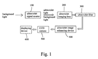
- An inorganic ultraviolet imaging inspection system generally comprises: an ultraviolet imaging object lens, an ultraviolet filter, an ultraviolet image enhancing system, a charge coupled device (CCD), and an image displaying system.
- An ultraviolet signal source 100 is irradiated by background light (including visible lights, ultraviolet light, and infrared light) and what is transmitted from the ultraviolet signal source 100 to an ultraviolet imaging lens 200 includes the ultraviolet light radiating from the ultraviolet signal source 100 itself and components of the background light reflected by the ultraviolet signal source 100 .
- An imaging ray after passing through the ultraviolet imaging lens 200 , is subjected to filtering of a portion of the background light, with a portion of the background lighting still remaining.
- the ray is then transmitted through an ultraviolet filter 300 , which allows for passage of light of the “solar blind range” only, to irradiate a photoelectrical cathode of an ultraviolet image enhancing device 400 .
- an ultraviolet filter 300 which allows for passage of light of the “solar blind range” only, to irradiate a photoelectrical cathode of an ultraviolet image enhancing device 400 .
- the ultraviolet signal is enhanced and amplified and converted into and output as a visible light signal.
- the imaging ray passes through a CCD camera 500 and is finally subjected to signal processing and supplied to a displaying device 600 for observation and recording.
- the materials that are used to make inorganic ultraviolet detectors include: first-generation elemental semiconductor materials, second-generation compound semiconductor materials, and third-generation wide band gap semiconductor materials.
- the first-generation elemental semiconductor materials primarily include silicon (Si);
- the second-generation compound semiconductor materials primarily include gallium arsenide (GaAs) and indium phosphide (InP);
- the third-generation wide band gap semiconductor materials primarily include silicon carbide (SiC), gallium nitride (GaN), zinc oxide (ZnO), and diamond.
- the first-generation semiconductor materials and the second-generation compound semiconductor materials impose heavy limitations to the characteristics and use of the ultraviolet detectors, making it not meeting the needs for practical applications.
- the third-generation wide band gap semiconductor materials have various characteristics, including large forbidden band width, high electron drafting saturation speed, small dielectric constant, and excellent thermal conductivity, making they perfectly suitable for electronic devices of radiation resistance, high frequency, large power, and high density integration.
- the unique forbidden bandwidth also allows them to be used to make light emitters or photo detection device of blue and green lights and ultraviolet light.
- the inorganic ultraviolet detection devices still suffer certain problems, such as high manufacturing cost, complicated operation, high material cost, and incapability of forming thin films on flexible plastic substrates.
- An object of the present invention is to provide an organic p-n junction based ultraviolet detection device, which has a simple structure, a small size, and a small weight, has a simple manufacturing process and a low manufacturing cost, can be manufactured with an organic material that has a low material cost, diversified categories, wide supplies, and can be manufactured with chemical synthesis, can be formed on a flexible substrate, and can expand wide angle of photographing.
- Another object of the present invention is to provide an ultraviolet image detector, which has simple structure, a small size, and a low weight, and has a simple manufacturing process and a low manufacturing cost due to using an organic p-n junction based ultraviolet detection device, and can use materials that are low in cost and diversified in categories and can be manufactured with chemical synthesis so that the ultraviolet image detector can have an expanded wide angle of photographing.
- an organic p-n junction based ultraviolet detection device which comprises: an active glass substrate and a packaging glass substrate that are arranged and opposite to and parallel with each other, a plurality of organic p-n junctions arranged between the active glass substrate and the packaging glass substrate, and a packaging material arranged along a circumferential edge area of the active glass substrate and the packaging glass substrate.
- the plurality of organic p-n junctions is arranged in the form of an array on the active glass substrate.
- Each of the organic p-n junctions comprises: an anode formed on the active glass substrate, an organic material layer formed on the anode, and a cathode formed on the organic material layer.
- the cathode and the packaging glass substrate contact each other.
- the organic material layer comprises an organic p-type material and an organic n-type material.
- the organic p-type material is an ultraviolet light emission material.
- the organic n-type material is fullerene derivative.
- the fullerene derivative has a molecular formula as follows:
- the fullerene derivative having an energy level of a highest occupied molecular orbital that is 6.0 eV and an energy level of a lowest unoccupied molecular orbital that is 4.2 eV and carrier mobility that is 10 ⁇ 3 cm 2 /V ⁇ s.
- the ultraviolet light emission material is a carbazole-based ultraviolet light emission material.
- the carbazole-based ultraviolet light emission material has a molecular formula as follows:
- the carbazole-based ultraviolet light emission material having a band gap that is 3.25 eV and a peak value of emission spectrum that is 394 nm.
- the ultraviolet light emission material is a pentacene-based ultraviolet light emission material.
- the pentacene-based ultraviolet light emission material has a molecular formula as follows:
- the pentacene-based ultraviolet light emission material having a band gap that is 3.48 eV and a peak value of emission spectrum that is 310 nm.
- the present invention also provides an organic p-n junction based ultraviolet detection device, which comprises: an active glass substrate and a packaging glass substrate that are arranged and opposite to and parallel with each other, a plurality of organic p-n junctions arranged between the active glass substrate and the packaging glass substrate, and a packaging material arranged along a circumferential edge area of the active glass substrate and the packaging glass substrate, the plurality of organic p-n junctions being arranged in the form of an array on the active glass substrate;
- the organic material layer comprises an organic p-type material and an organic n-type material.
- the organic p-type material is an ultraviolet light emission material.
- the organic n-type material is fullerene derivative.
- the fullerene derivative has a molecular formula as follows:
- the fullerene derivative having an energy level of a highest occupied molecular orbital that is 6.0 eV and an energy level of a lowest unoccupied molecular orbital that is 4.2 eV and carrier mobility that is 10 ⁇ 3 cm 2 /V ⁇ s.
- the ultraviolet light emission material is a carbazole-based ultraviolet light emission material.
- the carbazole-based ultraviolet light emission material has a molecular formula as follows:
- the carbazole-based ultraviolet light emission material having a band gap that is 3.25 eV and a peak value of emission spectrum that is 394 nm.
- the ultraviolet light emission material is a pentacene-based ultraviolet light emission material.
- the pentacene-based ultraviolet light emission material has a molecular formula as follows:
- the pentacene-based ultraviolet light emission material having a band gap that is 3.48 eV and a peak value of emission spectrum that is 310 nm.
- the present invention further provides an ultraviolet image detector using an organic p-n junction based ultraviolet detection device, comprising: an enclosure, an ultraviolet imaging lens mounted on the enclosure, an ultraviolet filter mounted on the enclosure and opposing the ultraviolet imaging lens, an organic p-n junction based ultraviolet detection device mounted in the enclosure and opposing the ultraviolet filter, a circuit structure mounted in the enclosure and electrically connected to the organic p-n junction based ultraviolet detection device, and a displaying device mounted on the enclosure and electrically connected to the circuit structure, the organic p-n junction based ultraviolet detection device comprising: an active glass substrate and a packaging glass substrate that are arranged and opposite to and parallel with each other, a plurality of organic p-n junctions arranged between the active glass substrate and the packaging glass substrate, and a packaging material arranged along a circumferential edge area of the active glass substrate and the packaging glass substrate, the plurality of organic p-n junctions being arranged in the form of an array on the active glass substrate.
- the active glass substrate of the organic p-n junction based ultraviolet detection device is set to face the ultraviolet filter, the enclosure comprising a first opening and a second opening, the ultraviolet imaging lens and the ultraviolet filter being mounted in the first opening, the ultraviolet filter being arranged behind the ultraviolet imaging lens, the displaying device being mounted in the second opening;
- Each of the organic p-n junctions comprises: an anode formed on the active glass substrate, an organic material layer formed on the anode, and a cathode formed on the organic material layer, the cathode and the packaging glass substrate contacting each other; and the organic material layer comprises an organic p-type material and an organic n-type material, the organic p-type material being an ultraviolet light emission material, the organic n-type material being fullerene derivative, the fullerene derivative having a molecular formula as follows:
- the fullerene derivative having an energy level of a highest occupied molecular orbital that is 6.0 eV and an energy level of a lowest unoccupied molecular orbital that is 4.2 eV and carrier mobility that is 10 ⁇ 3 cm 2 /V ⁇ s.
- the ultraviolet light emission material is a carbazole-based ultraviolet light emission material, the carbazole-based ultraviolet light emission material has a molecular formula as follows:
- the carbazole-based ultraviolet light emission material has a band gap that is 3.25 eV and a peak value of emission spectrum that is 394 nm.
- the ultraviolet light emission material is a pentacene-based ultraviolet light emission material, the pentacene-based ultraviolet light emission material has a molecular formula as follows:
- the pentacene-based ultraviolet light emission material has a band gap that is 3.48 eV and a peak value of emission spectrum that is 310 nm.
- the efficacy of the present invention is that the present invention provides an organic p-n junction based ultraviolet detection device and an ultraviolet image detector using the device, which use organic p-n junctions to absorb radiation photons of ultraviolet light and generates excitons (electron-hole pairs).
- the excitons are separated at an interface between an organic p-type material and an organic n-type material with electrons moving to a cathode and holes moving to an anode so as to form a photoelectric current.
- a circuit structure collects the photoelectric current, which is subjected to amplification and then used to finally display a monochromic image that is visible to human eyes on a displaying device.
- the image has a high contrast and a strong detail recognition power.
- the ultraviolet detection device has a simple structure, a small size, and a small weight, has a simple manufacturing process and a low manufacturing cost and can be manufactured with a material that is cheap and has diversified categories, wide supplies, and can be manufactured with chemical synthesis. Further, the ultraviolet detection device can be formed on a flexible substrate and can expand wide angle of photographing.
- FIG. 1 is a schematic view showing the principle of operation of a conventional inorganic ultraviolet imaging inspection system
- FIG. 2 is a schematic view showing the structure of an organic p-n junction based ultraviolet detection device according to the present invention
- FIG. 3 is a schematic view showing the arrangement of a plurality of organic p-n junctions in an organic p-n junction based ultraviolet detection device according to the present invention
- FIG. 4 is a schematic view illustrating the principle of generation of photoelectric current of the organic p-n junction based ultraviolet detection device according to the present invention
- FIG. 5 is a perspective view showing an ultraviolet image detector according to the present invention.
- FIG. 6 is a schematic view showing the connection of an electrical circuit of the ultraviolet image detector according to the present invention.
- FIG. 7 is a schematic view illustrating the principle of operation of the ultraviolet image detector according to the present invention.
- the present invention provides an organic p-n junction based ultraviolet detection device 40 , which uses a new-generation solar cell technique-organic solar cell technology-to manufacture a device structure that comprises a pixel dot array.
- the organic p-n junction based ultraviolet detection device 40 specifically comprises: an active glass substrate 42 and a packaging glass substrate 44 that are arranged and opposite to and parallel with each other, a plurality of organic p-n junctions 43 arranged between the active glass substrate 42 and the packaging glass substrate 44 , and a packaging material 48 arranged along a circumferential edge area of the active glass substrate 42 and the packaging glass substrate 44 .
- the plurality of organic p-n junctions 43 is arranged in the form of an array to facilitate enhancement of sensitivity of an ultraviolet image detector that uses the organic p-n junction based ultraviolet detection device 40 .
- Using the packaging material 48 to hermetically bond the active glass substrate 42 and the packaging glass substrate 44 to each other prevents moisture and oxygen from invading the interior of the packaged ultraviolet detection device 40 , maintaining the performance of the ultraviolet detection device 40 and extending the lifespan.
- Each of the organic p-n junctions 43 comprises: an anode 45 formed on the active glass substrate 42 , an organic material layer 46 formed on the anode 45 , and a cathode 47 formed on the organic material layer 46 , wherein the cathode 47 and the packaging glass substrate 44 contact each other.
- the organic material layer 46 includes an organic p-type material and an organic n-type material. Referring to FIG. 4 , the organic p-type material and the organic n-type material form therebetween an interface 87 .
- the organic material layer 46 absorbs external ultraviolet light 70 and forms excitons 82 (electrons-hole pairs).
- the excitons 82 can be acted on by an external voltage to divide, at the interface 87 , into holes 84 and electrons 86 , where the electrons 86 move to the cathode 47 and the holes 84 move to the anode 45 , so as to generate a photoelectric current.
- the organic p-type material is an ultraviolet light emission material, and the ultraviolet light emission material is preferably a carbazole-based ultraviolet light emission material, of which the molecular formula is:
- the ultraviolet light emission material can alternatively be a pentacene-based ultraviolet light emission material, of which the molecular formula is:
- the organic n-type material is preferably the fullerene derivative (PCBM), of which the molecular formula is:
- the energy level of HOMO highest occupied molecular orbital
- the energy level of LUMO lowest unoccupied molecular orbital
- carrier mobility 10 ⁇ 3 cm 2 /V ⁇ s
- the present invention also provides an ultraviolet image detector that uses the organic p-n junction based ultraviolet detection device and comprises: an enclosure 10 , an ultraviolet imaging lens 20 mounted on the enclosure 10 , an ultraviolet filter 30 mounted on the enclosure 10 and opposing the ultraviolet imaging lens 20 , an organic p-n junction based ultraviolet detection device 40 mounted in the enclosure 10 and opposing the ultraviolet filter 30 , a circuit structure 50 mounted in the enclosure 10 and electrically connected to the organic p-n junction based ultraviolet detection device 40 , and a displaying device 60 mounted on the enclosure 10 and electrically connected to the circuit structure 50 .
- the organic p-n junction based ultraviolet detection device 40 comprises: an active glass substrate 42 and a packaging glass substrate 44 that are arranged and opposite to each other, a plurality of organic p-n junctions 43 arranged between the active glass substrate 42 and the packaging glass substrate 44 , and a packaging material 48 arranged along a circumferential edge area of the active glass substrate 42 and the packaging glass substrate 44 .
- the plurality of organic p-n junctions 43 is arranged in the form of an array to facilitate enhancement of performance of the ultraviolet image detector.
- Using the packaging material 48 to hermetically bond the active glass substrate 42 and the packaging glass substrate 44 to each other prevents moisture and oxygen from invading the interior of the packaged ultraviolet detection device 40 , maintaining the performance of the ultraviolet detection device 40 and extending the lifespan.
- the active glass substrate 42 of the organic p-n junction based ultraviolet detection device 40 is set to face the ultraviolet filter 30 , whereby external ultraviolet light 70 , which passes through the ultraviolet imaging lens 20 and is filtered by the ultraviolet filter 30 , gets into the organic p-n junction based ultraviolet detection device 40 from the active glass substrate 42 .
- the enclosure 10 comprises a first opening 12 and a second opening 14 formed therein.
- the ultraviolet imaging lens 20 and the ultraviolet filter 30 are both mounted in the first opening 12 and the ultraviolet filter 30 is arranged behind the ultraviolet imaging lens 20 .
- External ultraviolet light 70 may directly irradiates a surface of the ultraviolet imaging lens 20 .
- the displaying device 60 is selectively mounted in the second opening 14 to display the intensity of the ultraviolet light 70 detected by the ultraviolet image detector, meaning displaying a monochromic image that is visible to human eyes. Further, the displaying device 60 may alternatively made separable from the enclosure 10 as a stand-alone device so as to be mountable at any location that can be easily observed by a user to enhance the operability thereof.
- the circuit structure 50 comprises: a photoelectric current collection and amplification module 52 electrically connected to the organic p-n junction based ultraviolet detection device 40 and a display driving module 54 electrically connected to the photoelectric current collection and amplification module 52 .
- the organic p-n junction based ultraviolet detection device 40 when irradiated by the ultraviolet light 70 , generates excitons 82 (electron-hole pairs).
- the excitons 82 eventually separate and generate a photoelectric current, whereby the photoelectric current collection and amplification module 52 detects the magnitude of the photoelectric current, namely detecting the intensity of the ultraviolet light 70 that irradiates the organic p-n junction based ultraviolet detection device 40 , and amplifies and transmits the photoelectric current to the display driving module 54 .
- the display driving module 54 is also electrically connected to the displaying device 60 and, according to the signal of the photoelectric current to drive the displaying device 60 to display a monochromic image.
- the brightness intensity of the monochromic image corresponds to the intensity of the ultraviolet light 70 that irradiates a corresponding area of the organic p-n junction based ultraviolet detection device 40 .
- Each of the organic p-n junctions 43 comprises: an anode 45 formed on the active glass substrate 42 , an organic material layer 46 formed on the anode 45 , and a cathode 47 formed on the organic material layer 46 , wherein the cathode 47 and the packaging glass substrate 44 contact each other.
- the organic material layer 46 includes an organic p-type material and an organic n-type material. Referring to FIG. 4 , the organic p-type material and the organic n-type material form therebetween an interface 87 .
- the organic material layer 46 absorbs external ultraviolet light 70 and forms excitons 82 (electrons-hole pairs).
- the excitons 82 can be acted on by an external voltage to divide, at the interface 87 , into holes 84 and electrons 86 , where the electrons 86 move to the cathode 47 and the holes 84 move to the anode 45 , so as to generate a photoelectric current.
- the photoelectric current flows through the circuit to the photoelectric current collection and amplification module 52 , by which the photoelectric current is amplified.
- the photoelectric current of each of the organic p-n junctions 43 after being collected and amplified, is finally applied to the displaying device 60 to form a monochromic image.
- the electrical current generated by each of the organic p-n junctions 43 has a magnitude corresponding to the brightness intensity of a corresponding area of the displaying device 60 .
- the organic p-type material is an ultraviolet light emission material, and the ultraviolet light emission material is preferably a carbazole-based ultraviolet light emission material, of which the molecular formula is:
- the ultraviolet light emission material can alternatively be a pentacene-based ultraviolet light emission material, of which the molecular formula is:
- the organic n-type material is preferably the fullerene derivative (PCBM), of which the molecular formula is:
- the energy level of HOMO highest occupied molecular orbital
- the energy level of LUMO lowest unoccupied molecular orbital
- carrier mobility 10 ⁇ 3 cm 2 /V ⁇ s
- the ultraviolet imaging lens 20 first filters out a portion of the external ultraviolet light 70 , and then, the ultraviolet filter 30 filter out visible light (wavelength ranging from 390 nm to 760 nm) and infrared wave band, with only ultraviolet light in the wave range of “the solar blind range” (240 nm-280 nm) preserved.
- the organic p-n junction based ultraviolet detection device 40 absorbs radiation photons of the ultraviolet light in the wave range of “the solar blind range” and generates excitons 82 (electron-hole pairs), whereby the excitons 82 are separated at an interface between an organic p-type material and an organic n-type material with electrons 86 moving to a cathode and holes 84 moving to an anode.
- the circuit structure 50 collects the photoelectric current, which is subjected to amplification and then used to finally display a monochromic image that is visible to human eyes on the displaying device 60 .
- the image has a high contrast and a strong detail recognition power.
- the ultraviolet detection device 40 has a simple structure, a small size, and a small weight, has a simple manufacturing process and a low manufacturing cost and can be manufactured with a material that is cheap and has diversified categories, wide supplies, and can be manufactured with chemical synthesis. Further, the ultraviolet detection device 40 can be formed on a flexible substrate and can expand wide angle of photographing.
- the present invention provides an organic p-n junction based ultraviolet detection device and an ultraviolet image detector using the device, which use organic p-n junctions to absorb radiation photons of ultraviolet light and generates excitons (electron-hole pairs).
- the excitons are separated at an interface between an organic p-type material and an organic n-type material with electrons moving to a cathode and holes moving to an anode so as to form a photoelectric current.
- a circuit structure collects the photoelectric current, which is subjected to amplification and then used to finally display a monochromic image that is visible to human eyes on a displaying device.
- the image has a high contrast and a strong detail recognition power.
- the ultraviolet detection device has a simple structure, a small size, and a small weight, has a simple manufacturing process and a low manufacturing cost and can be manufactured with a material that is cheap and has diversified categories, wide supplies, and can be manufactured with chemical synthesis. Further, the ultraviolet detection device can be formed on a flexible substrate and can expand wide angle of photographing.
Landscapes
- Engineering & Computer Science (AREA)
- Physics & Mathematics (AREA)
- Electromagnetism (AREA)
- Chemical & Material Sciences (AREA)
- Materials Engineering (AREA)
- Multimedia (AREA)
- Signal Processing (AREA)
- Spectroscopy & Molecular Physics (AREA)
- Nanotechnology (AREA)
- Photometry And Measurement Of Optical Pulse Characteristics (AREA)
- Electroluminescent Light Sources (AREA)
- Light Receiving Elements (AREA)
Abstract
Description

the fullerene derivative having an energy level of a highest occupied molecular orbital that is 6.0 eV and an energy level of a lowest unoccupied molecular orbital that is 4.2 eV and carrier mobility that is 10−3 cm2/V·s.

the carbazole-based ultraviolet light emission material having a band gap that is 3.25 eV and a peak value of emission spectrum that is 394 nm.
the pentacene-based ultraviolet light emission material having a band gap that is 3.48 eV and a peak value of emission spectrum that is 310 nm.
-
- wherein each of the organic p-n junctions comprises: an anode formed on the active glass substrate, an organic material layer formed on the anode, and a cathode formed on the organic material layer, the cathode and the packaging glass substrate contacting each other.

the fullerene derivative having an energy level of a highest occupied molecular orbital that is 6.0 eV and an energy level of a lowest unoccupied molecular orbital that is 4.2 eV and carrier mobility that is 10−3 cm2/V·s.

the carbazole-based ultraviolet light emission material having a band gap that is 3.25 eV and a peak value of emission spectrum that is 394 nm.
the pentacene-based ultraviolet light emission material having a band gap that is 3.48 eV and a peak value of emission spectrum that is 310 nm.
-
- the circuit structure comprising: a photoelectric current collection and amplification module electrically connected to the organic p-n junction based ultraviolet detection device and a display driving module electrically connected to the photoelectric current collection and amplification module, the display driving module being also electrically connected to the displaying device.

the fullerene derivative having an energy level of a highest occupied molecular orbital that is 6.0 eV and an energy level of a lowest unoccupied molecular orbital that is 4.2 eV and carrier mobility that is 10−3 cm2/V·s.

the carbazole-based ultraviolet light emission material has a band gap that is 3.25 eV and a peak value of emission spectrum that is 394 nm.
the pentacene-based ultraviolet light emission material has a band gap that is 3.48 eV and a peak value of emission spectrum that is 310 nm.

which has a band gap of 3.25 eV and a peak value of emission spectrum being 394 nm. The ultraviolet light emission material can alternatively be a pentacene-based ultraviolet light emission material, of which the molecular formula is:
which has a band gap of 3.48 eV and a peak value of emission spectrum being 310 nm.

which has excellent solubility and also has better electron transportation capability and higher electron affinity, the energy level of HOMO (highest occupied molecular orbital) being 6.0 eV, the energy level of LUMO (lowest unoccupied molecular orbital) being 4.2 eV, and carrier mobility being 10−3 cm2/V·s, so as to make it an excellent electron transportation material for solar cells.
Claims (13)


Applications Claiming Priority (4)
| Application Number | Priority Date | Filing Date | Title |
|---|---|---|---|
| CN201310574099.1A CN103594625B (en) | 2013-11-15 | 2013-11-15 | Ultraviolet detector based on organic p-n junction and use the ultraviolet image detector of this device |
| CN201310574099 | 2013-11-15 | ||
| CN201310574099.1 | 2013-11-15 | ||
| PCT/CN2013/087884 WO2015070485A1 (en) | 2013-11-15 | 2013-11-27 | Ultraviolet detection device based on organic p-n junctions and ultraviolet image detector using same |
Publications (2)
| Publication Number | Publication Date |
|---|---|
| US20150303240A1 US20150303240A1 (en) | 2015-10-22 |
| US9614009B2 true US9614009B2 (en) | 2017-04-04 |
Family
ID=50084685
Family Applications (1)
| Application Number | Title | Priority Date | Filing Date |
|---|---|---|---|
| US14/236,691 Active 2035-07-16 US9614009B2 (en) | 2013-11-15 | 2013-11-27 | Organic p-n junction based ultraviolet detection device and ultraviolet image detector using same |
Country Status (3)
| Country | Link |
|---|---|
| US (1) | US9614009B2 (en) |
| CN (1) | CN103594625B (en) |
| WO (1) | WO2015070485A1 (en) |
Families Citing this family (2)
| Publication number | Priority date | Publication date | Assignee | Title |
|---|---|---|---|---|
| CN111863893B (en) * | 2020-07-13 | 2022-04-05 | 武汉华星光电半导体显示技术有限公司 | Display panel and preparation method thereof |
| CN118099243B (en) * | 2024-04-25 | 2024-07-09 | 南京大学 | Packaging structure for deep ultraviolet wide-angle detection |
Citations (9)
| Publication number | Priority date | Publication date | Assignee | Title |
|---|---|---|---|---|
| CN1296645A (en) | 1998-02-02 | 2001-05-23 | 优尼爱克斯公司 | Image sensors made from organic semiconductors |
| US20050248260A1 (en) * | 2004-05-07 | 2005-11-10 | Sellars Mark J | Processes for removing organic layers and organic electronic devices formed by the processes |
| CN101345291A (en) | 2008-08-29 | 2009-01-14 | 华南理工大学 | Organic polymer thin film ultraviolet detector and preparation method thereof |
| US20090267060A1 (en) * | 2005-11-02 | 2009-10-29 | The Regents Of The Univerisity Of Michigan | Polymer wrapped carbon nanotube near-infrared photoactive devices |
| US20100095705A1 (en) * | 2008-10-20 | 2010-04-22 | Burkhalter Robert S | Method for forming a dry glass-based frit |
| CN101976728A (en) | 2010-09-29 | 2011-02-16 | 昆明物理研究所 | Photovoltaic organic ultraviolet semiconductor detector |
| US20110049367A1 (en) * | 2008-03-19 | 2011-03-03 | Stephen Forrest | Organic thin films for infrared detection |
| CN102244146A (en) | 2011-07-01 | 2011-11-16 | 中国科学院半导体研究所 | GaN-base ultraviolet detector area array which does not transmit infrared light and visible light |
| CN103390630A (en) | 2013-07-17 | 2013-11-13 | 深圳市华星光电技术有限公司 | Infrared detecting device based on organic p-n junctions, manufacturing method thereof and infrared image detector using device |
-
2013
- 2013-11-15 CN CN201310574099.1A patent/CN103594625B/en not_active Expired - Fee Related
- 2013-11-27 WO PCT/CN2013/087884 patent/WO2015070485A1/en active Application Filing
- 2013-11-27 US US14/236,691 patent/US9614009B2/en active Active
Patent Citations (10)
| Publication number | Priority date | Publication date | Assignee | Title |
|---|---|---|---|---|
| CN1296645A (en) | 1998-02-02 | 2001-05-23 | 优尼爱克斯公司 | Image sensors made from organic semiconductors |
| US20050248260A1 (en) * | 2004-05-07 | 2005-11-10 | Sellars Mark J | Processes for removing organic layers and organic electronic devices formed by the processes |
| US20090267060A1 (en) * | 2005-11-02 | 2009-10-29 | The Regents Of The Univerisity Of Michigan | Polymer wrapped carbon nanotube near-infrared photoactive devices |
| US20110049367A1 (en) * | 2008-03-19 | 2011-03-03 | Stephen Forrest | Organic thin films for infrared detection |
| CN101345291A (en) | 2008-08-29 | 2009-01-14 | 华南理工大学 | Organic polymer thin film ultraviolet detector and preparation method thereof |
| US20100095705A1 (en) * | 2008-10-20 | 2010-04-22 | Burkhalter Robert S | Method for forming a dry glass-based frit |
| CN101976728A (en) | 2010-09-29 | 2011-02-16 | 昆明物理研究所 | Photovoltaic organic ultraviolet semiconductor detector |
| CN102244146A (en) | 2011-07-01 | 2011-11-16 | 中国科学院半导体研究所 | GaN-base ultraviolet detector area array which does not transmit infrared light and visible light |
| CN103390630A (en) | 2013-07-17 | 2013-11-13 | 深圳市华星光电技术有限公司 | Infrared detecting device based on organic p-n junctions, manufacturing method thereof and infrared image detector using device |
| US20160118444A1 (en) * | 2013-07-17 | 2016-04-28 | Shenzhen China Star Optoelectronics Technology Co., Ltd. | Organic p-n junction based infrared detection device and manufacturing method thereof and infrared image detector using same |
Also Published As
| Publication number | Publication date |
|---|---|
| WO2015070485A1 (en) | 2015-05-21 |
| US20150303240A1 (en) | 2015-10-22 |
| CN103594625A (en) | 2014-02-19 |
| CN103594625B (en) | 2016-08-17 |
Similar Documents
| Publication | Publication Date | Title |
|---|---|---|
| Hadfield et al. | Single-photon detection for long-range imaging and sensing | |
| US20230134972A1 (en) | Hole transporting material for helios | |
| CN109417085B (en) | Solid-state image pickup element and solid-state image pickup device | |
| US20230292614A1 (en) | Photoelectric conversion element and solid-state imaging device | |
| WO2018016215A1 (en) | Photoelectric conversion element and solid-state image pickup device | |
| CN107863411B (en) | Polarization imaging detector | |
| Fraenkel et al. | High definition 10μm pitch InGaAs detector with asynchronous laser pulse detection mode | |
| US20150228813A1 (en) | Continuous resonant trap refractors, lateral waveguides and devices using same | |
| US20220271245A1 (en) | Photoelectric conversion element and solid-state imaging apparatus | |
| Pecunia | Organic Narrowband Photodetectors: Materials, Devices and Applications | |
| US9614009B2 (en) | Organic p-n junction based ultraviolet detection device and ultraviolet image detector using same | |
| Gundepudi et al. | A review on the role of nanotechnology in the development of near-infrared photodetectors: materials, performance metrics, and potential applications | |
| US20160118444A1 (en) | Organic p-n junction based infrared detection device and manufacturing method thereof and infrared image detector using same | |
| Rao et al. | Infrared-to-visible upconversion devices | |
| US11322547B2 (en) | Photoelectric conversion element and solid-state imaging device | |
| Goel et al. | Self-powered photodetectors: a device engineering perspective | |
| EP4053926A1 (en) | Photoelectric conversion element and imaging element | |
| Gunapala et al. | Recent developments and applications of quantum well infrared photodetector focal plane arrays | |
| Hu et al. | Visualization of invisible near-infrared light | |
| US20220407019A1 (en) | Photoelectric conversion element and imaging device | |
| US20220231246A1 (en) | Photoelectric conversion element and imaging device | |
| CN106898674A (en) | A kind of double-waveband detector | |
| WO2019203013A1 (en) | Photoelectric conversion element and imaging device | |
| US20130126711A1 (en) | Low light vision and thermal imaging devices with cool chip cooling | |
| Fu et al. | Advances in Organic Upconversion Devices |
Legal Events
| Date | Code | Title | Description |
|---|---|---|---|
| AS | Assignment |
Owner name: SHENZHEN CHINA STAR OPTOELECTRONICS TECHNOLOGY CO. Free format text: ASSIGNMENT OF ASSIGNORS INTEREST;ASSIGNOR:LIU, YAWEI;REEL/FRAME:032117/0453 Effective date: 20130113 |
|
| FEPP | Fee payment procedure |
Free format text: PAYOR NUMBER ASSIGNED (ORIGINAL EVENT CODE: ASPN); ENTITY STATUS OF PATENT OWNER: LARGE ENTITY |
|
| STCF | Information on status: patent grant |
Free format text: PATENTED CASE |
|
| MAFP | Maintenance fee payment |
Free format text: PAYMENT OF MAINTENANCE FEE, 4TH YEAR, LARGE ENTITY (ORIGINAL EVENT CODE: M1551); ENTITY STATUS OF PATENT OWNER: LARGE ENTITY Year of fee payment: 4 |