US9601370B2 - Nonvolatile semiconductor memory device and method of manufacturing the same - Google Patents
Nonvolatile semiconductor memory device and method of manufacturing the same Download PDFInfo
- Publication number
- US9601370B2 US9601370B2 US14/645,985 US201514645985A US9601370B2 US 9601370 B2 US9601370 B2 US 9601370B2 US 201514645985 A US201514645985 A US 201514645985A US 9601370 B2 US9601370 B2 US 9601370B2
- Authority
- US
- United States
- Prior art keywords
- contact
- conductive layers
- select transistor
- memory device
- nonvolatile semiconductor
- Prior art date
- Legal status (The legal status is an assumption and is not a legal conclusion. Google has not performed a legal analysis and makes no representation as to the accuracy of the status listed.)
- Active
Links
Images


Classifications
-
- H—ELECTRICITY
- H01—ELECTRIC ELEMENTS
- H01L—SEMICONDUCTOR DEVICES NOT COVERED BY CLASS H10
- H01L21/00—Processes or apparatus adapted for the manufacture or treatment of semiconductor or solid state devices or of parts thereof
- H01L21/70—Manufacture or treatment of devices consisting of a plurality of solid state components formed in or on a common substrate or of parts thereof; Manufacture of integrated circuit devices or of parts thereof
- H01L21/71—Manufacture of specific parts of devices defined in group H01L21/70
- H01L21/768—Applying interconnections to be used for carrying current between separate components within a device comprising conductors and dielectrics
- H01L21/76838—Applying interconnections to be used for carrying current between separate components within a device comprising conductors and dielectrics characterised by the formation and the after-treatment of the conductors
- H01L21/76877—Filling of holes, grooves or trenches, e.g. vias, with conductive material
-
- H—ELECTRICITY
- H01—ELECTRIC ELEMENTS
- H01L—SEMICONDUCTOR DEVICES NOT COVERED BY CLASS H10
- H01L21/00—Processes or apparatus adapted for the manufacture or treatment of semiconductor or solid state devices or of parts thereof
- H01L21/70—Manufacture or treatment of devices consisting of a plurality of solid state components formed in or on a common substrate or of parts thereof; Manufacture of integrated circuit devices or of parts thereof
- H01L21/71—Manufacture of specific parts of devices defined in group H01L21/70
- H01L21/768—Applying interconnections to be used for carrying current between separate components within a device comprising conductors and dielectrics
- H01L21/76801—Applying interconnections to be used for carrying current between separate components within a device comprising conductors and dielectrics characterised by the formation and the after-treatment of the dielectrics, e.g. smoothing
- H01L21/76802—Applying interconnections to be used for carrying current between separate components within a device comprising conductors and dielectrics characterised by the formation and the after-treatment of the dielectrics, e.g. smoothing by forming openings in dielectrics
- H01L21/76816—Aspects relating to the layout of the pattern or to the size of vias or trenches
-
- H—ELECTRICITY
- H01—ELECTRIC ELEMENTS
- H01L—SEMICONDUCTOR DEVICES NOT COVERED BY CLASS H10
- H01L21/00—Processes or apparatus adapted for the manufacture or treatment of semiconductor or solid state devices or of parts thereof
- H01L21/70—Manufacture or treatment of devices consisting of a plurality of solid state components formed in or on a common substrate or of parts thereof; Manufacture of integrated circuit devices or of parts thereof
- H01L21/71—Manufacture of specific parts of devices defined in group H01L21/70
- H01L21/768—Applying interconnections to be used for carrying current between separate components within a device comprising conductors and dielectrics
- H01L21/76838—Applying interconnections to be used for carrying current between separate components within a device comprising conductors and dielectrics characterised by the formation and the after-treatment of the conductors
-
- H—ELECTRICITY
- H01—ELECTRIC ELEMENTS
- H01L—SEMICONDUCTOR DEVICES NOT COVERED BY CLASS H10
- H01L23/00—Details of semiconductor or other solid state devices
- H01L23/52—Arrangements for conducting electric current within the device in operation from one component to another, i.e. interconnections, e.g. wires, lead frames
- H01L23/522—Arrangements for conducting electric current within the device in operation from one component to another, i.e. interconnections, e.g. wires, lead frames including external interconnections consisting of a multilayer structure of conductive and insulating layers inseparably formed on the semiconductor body
- H01L23/5226—Via connections in a multilevel interconnection structure
-
- H01L27/11565—
-
- H01L27/11575—
-
- H01L27/11582—
-
- H—ELECTRICITY
- H10—SEMICONDUCTOR DEVICES; ELECTRIC SOLID-STATE DEVICES NOT OTHERWISE PROVIDED FOR
- H10B—ELECTRONIC MEMORY DEVICES
- H10B43/00—EEPROM devices comprising charge-trapping gate insulators
- H10B43/10—EEPROM devices comprising charge-trapping gate insulators characterised by the top-view layout
-
- H—ELECTRICITY
- H10—SEMICONDUCTOR DEVICES; ELECTRIC SOLID-STATE DEVICES NOT OTHERWISE PROVIDED FOR
- H10B—ELECTRONIC MEMORY DEVICES
- H10B43/00—EEPROM devices comprising charge-trapping gate insulators
- H10B43/20—EEPROM devices comprising charge-trapping gate insulators characterised by three-dimensional arrangements, e.g. with cells on different height levels
- H10B43/23—EEPROM devices comprising charge-trapping gate insulators characterised by three-dimensional arrangements, e.g. with cells on different height levels with source and drain on different levels, e.g. with sloping channels
- H10B43/27—EEPROM devices comprising charge-trapping gate insulators characterised by three-dimensional arrangements, e.g. with cells on different height levels with source and drain on different levels, e.g. with sloping channels the channels comprising vertical portions, e.g. U-shaped channels
-
- H—ELECTRICITY
- H10—SEMICONDUCTOR DEVICES; ELECTRIC SOLID-STATE DEVICES NOT OTHERWISE PROVIDED FOR
- H10B—ELECTRONIC MEMORY DEVICES
- H10B43/00—EEPROM devices comprising charge-trapping gate insulators
- H10B43/50—EEPROM devices comprising charge-trapping gate insulators characterised by the boundary region between the core and peripheral circuit regions
Definitions
- Embodiments described herein relate to a nonvolatile semiconductor memory device and a method of manufacturing the same.
- NAND type flash memory devices of laminating type are attracting attention, as devices enabled to achieve high integration without resolution limit of lithography technologies.
- Such NAND type flash memory devices of three-dimensional type comprise a stacked body configured by alternately stacking conductive films which function as word lines or select gate lines and interlayer insulating films. In addition, It also comprises semiconductor layers formed to penetrate the stacked body. These semiconductor layers function as bodies of the memory strings. A memory film including a charge storage film is formed between the semiconductor layer and the conductive films.
- ON/OFF properties of the select transistors are important. It is necessary to flow a sufficient current when it is selected, while it is necessary to suppress a leak current when it is not selected.
- an area of a wiring region for connection to various wiring lines is required to be reduced.
- FIG. 1 is a perspective view schematically illustrating one example of a structure of a nonvolatile semiconductor memory device 100 according to the first embodiment.
- FIG. 2 is a perspective view illustrating a part of a structure of the memory cell array 11 .
- FIG. 3 is an equivalent circuit diagram of one NAND cell unit NU.
- FIG. 4A is a perspective sectional view of one memory cell MC.
- FIG. 4B is a schematic perspective view of one drain-side select transistor S 1 or source-side select transistor S 2 .
- FIG. 5 is a plan view of a part of the memory cell array 11 .
- FIG. 6 is a sectional view along the Y direction of the memory cell array 11 (a sectional view of X-X′ direction of FIG. 5 ).
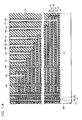
- FIG. 7 is a plan view illustrating an example of the structure of the wiring section 20 .
- FIG. 8 is a sectional view of the X-direction of the wiring section 20 (D-D′ sectional view of FIG. 7 ).
- FIG. 9 is a schematic perspective view illustrating one example of a structure of the wiring section 20 .
- FIG. 10 is a schematic perspective view illustrating one example of a structure of the wiring section 20 .
- FIG. 11A is an enlarged cross-sectional view illustrating a structure of the wiring section 20 .
- FIG. 11B is a more-enlarged view of the conductive layers 22 (select gate lines SGS and SGD) of the select transistor S 1 or S 2 .
- FIG. 11C is a more-enlarged view of the conductive layers 22 (word lines WL) of the memory cells MC.
- FIG. 12 is a process chart illustrating a manufacturing method of the memory cell array 11 and the wiring section 20 .
- FIG. 13 is a process chart illustrating a manufacturing method of the memory cell array 11 and the wiring section 20 .
- FIG. 14 is a process chart illustrating a manufacturing method of the memory cell array 11 and the wiring section 20 .
- FIG. 15 is a process chart illustrating a manufacturing method of the memory cell array 11 and the wiring section 20 .
- FIG. 16 is a process chart illustrating a manufacturing method of the memory cell array 11 and the wiring section 20 .
- FIG. 17 is a process chart illustrating a manufacturing method of the memory cell array 11 and the wiring section 20 .
- FIG. 18 is a sectional view illustrating the structure of the nonvolatile semiconductor memory device according to the second embodiment.
- FIG. 19 is a sectional view illustrating the structure of the nonvolatile semiconductor memory device according to the third embodiment.
- FIG. 20 is a sectional view illustrating the structure of the nonvolatile semiconductor memory device according to the fourth embodiment.
- FIG. 21 is a sectional view illustrating the structure of the nonvolatile semiconductor memory device according to the fourth embodiment.
- FIGS. 22 to 33 show modified examples.
- the memory cell array includes a memory string and a select transistor.
- the memory string includes a plurality of memory cells connected in series, the memory string being formed to extend in a first direction.
- the select transistor is connected to one end of the memory string.
- a conductive layer and an interlayer insulating layer are laminated alternately to form plural layers.
- the conductive layer functions as a gate electrode of the memory cells and the select transistor.
- One select transistor includes the plurality of the conductive layers, and the plurality of the conductive layers are connected in common by a common first contact.
- the plurality of the conductive layers and the first contact include a barrier metal formed in a periphery thereof. The plurality of the conductive layers and the first contact without the barrier metal therebetween at a boundary thereof.
- nonvolatile semiconductor memory device according to an embodiment will be described with reference to the drawings in detail.
- these embodiments are mere examples, and are not shown for limiting the scope of the present invention.
- the nonvolatile semiconductor memory device described hereinbelow has a structure in which a memory string extends in a straight line along a vertical direction to a substrate, but the present invention is applicable to a device in which a memory string has a U-shaped form in which the memory string is folded back in an opposite direction on the way.
- each of the drawings of the nonvolatile semiconductor memory device used in the following embodiments are schematic ones. The thickness, width, ratio and the like of the layers are different from actual ones.
- the embodiment described hereinbelow relates to a non-volatile semiconductor memory device having a structure in which a plurality of MONOS (Metal-Oxide-Nitride-Oxide-Semiconductor) type memory cells (transistors) are provided in a height direction.
- the MONOS type memory cells includes a semiconductor film as a channel provided in a pillar shape that is perpendicular to the substrate, and a gate electrode film provided on a side surface of the semiconductor film via a charge storage layer.
- MONOS Metal-Oxide-Nitride-Oxide-Semiconductor
- the embodiments may be applicable to memory cells having another types of charge storage layer, e.g., SONOS-type (Semiconductor-Oxide-Nitride-Oxide-Semiconductor) memory cell, or memory cells of a floating-gate type.
- SONOS-type semiconductor-Oxide-Nitride-Oxide-Semiconductor
- FIG. 1 is a perspective view schematically illustrating an example of a structure of a nonvolatile semiconductor memory device 100 according to the first embodiment.
- the nonvolatile semiconductor memory device 100 includes a memory cell array 11 , a word line driver circuit 12 , a source-side select gate line drive circuit 13 , a drain-side select gate line drive circuit 14 , a sense amplifier 15 , word lines WL, source-side select gate lines SGS, drain-side select gate lines SGD, bit lines BL, word-line wiring regions, and the like.
- the memory cell array 11 includes, on a semiconductor substrate (not illustrated in FIG. 1 ), a memory string MS in which a plurality of memory cells MC (memory transistor) are serially connected, a drain-side select transistor S 1 and a source-side select transistor S 2 which are connected to both ends of the memory string MS, respectively.
- a memory string MS in which a plurality of memory cells MC (memory transistor) are serially connected
- a drain-side select transistor S 1 and a source-side select transistor S 2 which are connected to both ends of the memory string MS, respectively.
- NAND cell unit NU the memory string MS, the drain-side select transistor S 1 and the source-side select transistor S 2 that are connected to both ends thereof.
- the memory cell MC has a structure in which a control gate electrode (word line) is provided on a side surface of a columnar-shaped semiconductor film functioning as a channel, via a memory film including the charge storage layer.
- a control gate electrode word line
- the drain-side select transistor and source-side select transistor each have a structure in which a select gate electrode (select gate line) is provided on a side surface of a columnar-shaped semiconductor film, via a memory film including the charge storage layer.
- FIG. 1 exemplifies, for simplification of illustration, a case where four memory cells MC are provided in one memory string MS. It goes without saying that the number of memory cells MC in one memory string MS is not limited to this example.
- the word lines WL are connected in common to the memory cells adjoining in the X direction (word-line direction) in FIG. 1 .
- the source-side select gate line SGS is connected in common to the source-side select transistors S 2 adjoining in the word-line direction.
- the drain-side select gate line SGD is connected in common to the drain-side select transistors S 1 adjoining in the word-line direction.
- the source-side select gate line SGS and the drain-side select gate line SGD may be collectively and merely called “a select gate line” in the later explanation.
- a source-side select transistor and a drain-side select transistor may be collectively and merely named “a select transistor”. Note that, among the memory cells MC in the memory string MS, one or more memory cells MC adjacent to the source-side select gate line SGS and the drain-side select gate line SGD may be dealt as dummy cells which are not used for storing data.
- each of the both ends of the memory string MS is provided with one dummy cell, respectively, it does not mean that the scope of the present invention is limited to these examples.
- the dummy cells may be two or more, or it is possible to omit the dummy cells.
- bit lines BL are arranged to extend along the Y direction (bit-line direction) that is a lengthwise direction and intersects the X direction (word-line direction). Also, the bit lines BL are arranged with a certain pitch in the X direction.
- the bit lines BL are connected to a plurality of the memory string MS via the drain-side select transistors S 1 . Although the illustration of the source line SL is omitted in FIG. 1 , the source line SL is arranged having the Y direction as its lengthwise direction, and is connected to the memory string MS via the source-side select transistor S 2 .
- a word line driver circuit 12 is a circuit that controls the voltages applied to the word lines WL.
- a source-side select gate line drive circuit 13 is a circuit that controls the voltages applied to the source-side select gate lines SGS.
- a drain-side select gate line drive circuit 14 is a circuit that controls the voltages applied to the drain-side select gate lines SGD.
- a sense amplifier 15 is a circuit that amplifies a signal (a voltage) read to the bit lines BL from selected memory cells.
- a wiring section 20 is a wiring section that connects the word lines WL and the select gate lines SGD, SGS to contacts.
- the word line WL and the select gate lines SGS, SGD have structures processed in the shape of stairs so as to be connected to the contacts independently at their upper parts thereof, respectively.
- FIG. 2 is a perspective view illustrating a part of the structure of the memory cell array 11 .
- FIG. 3 is an equivalent circuit diagram of one NAND cell unit NU.
- FIG. 4A is a perspective sectional view of one memory cell MC or the like, and
- FIG. 4B is also a schematic perspective diagram of one drain-side select transistor S 1 or source-side select transistor S 2 .
- the memory cell array 11 has a structure in which interlayer insulating layers 21 and conductive films 22 are alternately stacked on a semiconductor substrate SB. These conductive films 22 function as control gates (word lines WL) of the memory cells MC, the source-side select gate lines SGS and the drain-side select gate lines SGD.
- the interlayer insulating layers 21 are arranged above and below these conductive films 22 to insulate the conductive films 22 from one another.
- the conductive films 22 may be formed, for example, by tungsten (W), tungsten nitride (WN), tungsten silicide (WSi x ), tantalum (Ta), tantalum nitride (TaN), tantalum silicide (TaSix), palladium silicide (PdSi x ), erbium silicide (ErSi x ), yttrium silicide (YSi x ), platinum silicide (PtSi x ), hafnium silicide (HfSi x ), nickel silicide (NiSi x ), cobalt silicide (CoSi x ), titanium silicide (TiSi x ), vanadium silicide (VSi x ), chromium silicide (CrSi x ), manganese silicide (MnSi x ), iron silicide (FeSi x ), ruthenium (Ru),
- a laminated film CF including a block insulating film 105 , a block high-k dielectric film 106 and a barrier metal 107 . This will be described later.
- semiconductor layers 23 are arranged having a stacking direction (Z direction) as their lengthwise direction, and arranged in certain pitches in the XY plane, so as to penetrate a stack of such the interlayer insulating layers 21 and conductive films 22 .
- a memory film 24 including a charge storage layer Formed between the semiconductor layer 23 and the conductive film 22 and the interlayer insulating layer 21 is a memory film 24 including a charge storage layer.
- the memory film 24 may be formed of a laminated structure of a charge storage film such as a silicon nitride film, and an oxide film such as a silicon oxide film, as described below.
- a threshold voltage of the memory cell MC changes depending on the amount of electric charges stored in the charge storage film.
- the memory cell MC stores data corresponding to this threshold voltage.
- the semiconductor layers 23 function as a channel region (body) of the memory cells MC, the dummy cells DMC 1 , DMC 2 and the select transistors S 1 , S 2 that are included in the NAND cell unit NU. These semiconductor layers 23 are connected to the bit lines BL via contacts Cb at their upper ends.
- the bit lines BL are arranged having the Y direction as their lengthwise direction, and arranged in a certain pitch in the X direction.
- the lower ends of the semiconductor layers 23 are connected to the semiconductor substrate SB. As described below, the lower ends of the semiconductor layers 23 are connected to the source line SL via this semiconductor substrate SB and a source contact LI described below.
- the source line SL is arranged having the Y direction as its lengthwise direction, similar to the bit line BL.
- the stack of the interlayer insulating layers 21 and the conductive films 22 in the memory cell array 11 is divided into blocks each of which is the smallest unit for data erase. Trenches Tb are formed at the boundaries of the division. An interlayer insulating layer not illustrated is embedded in these trenches Tb. Furthermore, the above-described source contact LI is formed to penetrate the interlayer insulating layer. This source contact LI has a lower end connected to the semiconductor substrate SB, and an upper end connected to the source line SL.
- FIG. 3 is an equivalent circuit diagram of one NAND cell unit NU.
- one NAND cell unit includes: the memory string MS having the plural memory cells MC, and the dummy cells DMC 1 ,DMC 2 ; the drain-side select transistor S 1 connected between the upper end of the memory string MS and the bit line BL; and the source-side select transistor S 2 connected between the lower end of the memory string and the source line SL.
- the semiconductor layer 23 includes an oxide film core 101 a , and a semiconductor pillar member 102 that surrounds the periphery of the oxide film core 101 a .
- the oxide film core 101 is formed of a silicon oxide film (SiO 2 ), for example.
- the semiconductor pillar member 102 is formed of, for example, silicon (Si), silicon germanium (SiGe), silicon carbide (SiC), germanium (Ge) or carbon (C).
- the tunnel insulating film 103 is formed of a silicon oxide film (SiO x ), for example, and functions as a tunnel insulating film of the memory cell MC or the dummy cell DMC.
- the charge storage layer 104 is formed of a silicon nitride film (SiN), for example, and has a function of causing trap of electrons injected from the semiconductor pillar member 102 via the tunnel insulating film 103 due to a write operation.
- the tunnel insulating film 103 and the charge storage layer 104 are illustrated to be formed on the entire side surface of the semiconductor pillar member 102 . However, they are not limited to this example. They may be formed only on the side surfaces of the word lines WL.
- the above-mentioned interlayer insulating layers 21 and tungsten electrodes 108 functioning as the conductive film 22 .
- formed around the tungsten electrode 108 are the block insulating film 105 , the block high-k dielectric film 106 and the barrier metal 107 . They surround the tungsten electrode 108 in this order from outside.
- the block insulating film 105 may be formed of, for example, a silicon oxide film.
- the block insulating film 105 is formed to cover the periphery of the tungsten electrode 108 .
- it similarly to the tunnel insulating film 103 and the charge storage film 104 , it can be formed on the entire side surface of the semiconductor pillar member 102 .
- the material of the tunnel insulating film 103 and the block insulating film 105 it is possible to adopt, in addition to a silicon oxide film (SiOx), Al 2 O 3 , Y 2 O 3 , La 2 O 3 , Gd 2 O 3 , Ce 2 O 3 , CeO 2 , Ta 2 O 5 , HfO 2 , ZrO 2 , TiO 2 , HfSiO, HfAlO, ZrSiO, ZrAlO, AlSiO and the like, for example.
- SiOx silicon oxide film
- FIG. 4B is a perspective diagram illustrating the structure of one drain-side select transistor S 1 or source-side select transistor S 2 .
- One drain-side select transistor S 1 or source-side select transistor S 2 comprises a plurality of the conductive films 22 , the memory film 24 which are adjacent to the semiconductor layers 23 in the XY plane.
- the plural conductive films 22 connected to one select transistor S 1 or S 2 are short-circuited electrically by a contact (not illustrated in FIG. 4B ) that penetrates these conductive films 22 , thereby functioning as a single gate electrode.
- one select transistor S 1 or S 2 in this first embodiment comprises a plurality of short-circuited conductive films 22 .
- Such structure is employed for improving selection characteristics of the select transistors S 1 and S 2 . That is, it is necessary to suppress a leak current in unselected select transistors S 1 and S 2 as low as possible.
- FIG. 5 is a plan view of a part of the memory cell array 11
- FIG. 6 is also a sectional view along the Y direction of the memory cell array 11 (a sectional view of the X-X′ direction of FIG. 5 ).
- FIG. 7 is a plan view of the wiring section 20 .
- FIG. 8 is a sectional view of the X direction of the wiring section 20 (D-D′ sectional view of FIG. 7 ).
- the semiconductor layers 23 are arranged along one line in an oblique direction with respect to the X direction (word-line direction) and the Y direction (bit-line direction), thereby increasing the arrangement concentration of the semiconductor layers 23 , and increasing the arrangement concentration of the memory cells MC.
- the source contact LI is formed to have a stripe shape with the X direction as its lengthwise direction, and is embedded in the trench Tb via the interlayer insulating layer 21 ′.
- many trenches Ta are formed to penetrate the interlayer insulating layers 21 and the conductive films 22 laminated on the semiconductor substrate SB.
- the memory film 24 (a laminated films of the tunnel insulating film 103 and the charge storage layer 104 ) is formed along the sidewall of the trench Ta. Furthermore, the semiconductor layer 23 is embedded inside the trench Ta.
- the conductive film 22 is formed in contact with the memory film 24 .
- the above-mentioned laminated film CF (the laminated film of the block insulating film 105 , the block high-k dielectric film 106 and the barrier metal 107 ) is formed around the conductive film 22 . That is, the conductive film 22 contacts with the memory film 24 via this laminated film CF.
- the above-described source contact LI is embedded in the trench Tb that divides the memory cell array 11 in a block basis, via the interlayer insulating layer 21 ′.
- the lower end of the source contact LI contacts with the diffusion layer 26 formed on the surface of the substrate SB, and the upper end thereof is connected to the source line SL through an upper wiring line.
- the wiring section 20 is a wiring region for connecting the conductive layers 22 that function as the word lines WL or the select gate lines SGD, SGS to an external circuit via the contacts.
- the conductive layers 22 that function as the word lines WL are formed to have a step-like shape in this wiring section 20 together with the interlayer insulating layer 21 . Due to this, the conductive layers 21 may be independently connected to the contacts on upper surfaces thereof, respectively.
- the conductive layers 22 functioning as the word lines WL are connected to the word line driver circuit 12 shown in FIG. 1 by contacts Cw. Note that the contacts Cw are embedded, via barrier metal BM, in trenches formed in the interlayer insulating layer 21 ′ that buries the wiring section 20 .
- the conductive layers 22 functioning as the drain-side select gate lines SGD are processed such that their ends in the X direction (the lengthwise direction of the select gate line) are aligned, not in a step-like shape.
- the plural select gate lines SGD (the conductive layers 22 ) connected to one drain-side select transistor S 1 (in the example in FIG. 8 , three) are short-circuited by a common contact BS that penetrates them.
- a common contact BS By forming the contact BS that penetrates a plurality of the conductive layers 22 whose ends are aligned in the X direction, an area occupied by the drain-side select gate lines BS may become small. This may contribute to reduction of the area of the entire non-volatile semiconductor memory device.
- a contact is formed to penetrate a plurality of conductive layers 22 that is made of metal such as tungsten, the process of penetrating metal films is highly difficult. However, such a structure may be easily processed by adopting a manufacturing method described below.
- the above-mentioned laminated film CF (a laminated film of the block insulating film 105 , the block high-k dielectric film 106 and the barrier metal 107 ) is formed at the periphery of the plurality of the conductive layers 22 and the contacts BS.
- the plurality of the conductive layers 22 and the contacts BS are in contact without any laminated film CF (including the barrier metal) at their boundaries.
- the conductive layers 22 functioning as the source-side select gate lines SGS are processed such that their ends in the X direction are aligned, not in a step-like shape.
- the plurality of the select gate lines SGS (the conductive layers 22 ) connected to one source-side select transistor S 2 are short-circuited by the common contact BS.
- the above-mentioned laminated film CF (a laminated film of the block insulating film 105 , the block high-k dielectric film 106 and the barrier metal 107 ) is formed at the periphery of the plurality of the conductive layers 22 and the contacts BS.
- the plurality of the conductive layers 22 and the contacts BS are in contact without any laminated film CF (including the barrier metal) at their boundaries. By contacting without any barrier metal therebetween, the interface resistance between them is reduced, and the resistance of the select gate line SGS may be reduced.
- the conductive layers 22 are formed by, as described in detail later, after sacrifice films has been removed by wet etching, embedding a conductive material in a gap where the sacrifice film has been removed. Accordingly, the wiring section 20 comprises slit regions CC located at a certain interval, as shown in FIG. 7 .
- the sacrifice film is removed by wet etching solution that enters through the slit regions CC.
- the above-mentioned laminated film CF and the conductive layers 22 are deposited using a chemical vapor deposition (CVD) method. After the laminated film CF and the conductive layers 22 have been deposited, an insulating film is buried in the slit regions CC.
- the conductive layers 22 constituting the word lines WL may have a step-like portion extending in one direction only in the X direction as shown in FIG. 9 , or they may have a step-like portion extending two-dimensionally as shown in FIG. 10 .
- FIG. 11A is an expanded sectional view illustrating the structure of the wiring section 20 .
- FIG. 11B is a further enlarged view of the part of the conductive layers 22 of the select transistor S 1 or S 2 (the select gate lines SGS, SGD).
- FIG. 11C is a further enlarged view of the part of the conductive layer 22 s of the memory cells MC (the word lines WL).
- the wiring section 20 includes support members HR, as shown in FIG. 11A .
- the support member HR has a role of supporting the interlayer insulating layers after removing the sacrifice films for forming the word lines WL, and the select gate lines SGD, SGS, in order to avoid the collapsing of the left interlayer insulating layers.
- the support members HR are formed of the same material as that of the interlayer insulating layer, for example, a silicon oxide film, and are formed in the wiring section 20 at a certain interval.
- the contact BS is separated from the end portion of the support member HR by a distance of 20 nm or more, and is arranged within the distance of 1000 nm from the center of the support member HR. More preferably, in consideration of the collapsing risk due to stress, it is arranged within the distance of 400 nm from the center of the support member HR. This is because, when the contact BS is away from the support member HR by a distance of 1000 nm or more, the risk of collapsing of the wiring section 20 may become larger in the removal process of the sacrifice film.
- FIG. 11A illustrates two support member HR, this is merely an example, and it is not limited to this example.
- the support member HR penetrates not only the select gate lines SGS or SGD but also the word lines WL to prevent collapsing of the structure where the word lines WL are formed.
- a plurality of the conductive layers 22 forming the select gate lines SGS or SGD are commonly connected by the contact BS penetrating through them.
- this contact BS is formed by a process that is identical to that of the plural conductive layers 22 forming the select gate lines SGS and SGD, and at the same time as the plural conductive layers.
- the contacts BS are connected seamlessly to the conductive layers 22 , without being divided by the laminated film CF (barrier metal) at the boundaries therebetween.
- the laminated film CF is formed only at the periphery of the final structures of the conductive layer 22 and the contacts BS, but is not formed at the boundary between the conductive layers 22 and the contacts BS. This structure may be obtained because the manufacturing method to be described below is adopted.
- a plurality of the conductive layers 22 that form the word lines WL are connected to the different contacts Cw, respectively, via the barrier metal BM.
- the contacts Cw are formed by a process that is different from the process of depositing a plurality of the conductive layers 22 that are to be the word lines WL.
- the barrier metal BM is also formed in the boundary between the contacts Cw and the conductive layers 22 that are to be the word lines WL.
- the contacts Cw may be formed by the same process as that of the conductive layers 22 , similar to the contacts BS. In this case, the contacts Cw and the conductive layers 22 for the word lines WL may be connected seamlessly, without forming the barrier metal BM at the boundary thereof.
- the interlayer insulating layers 21 formed of silicon oxide films, for example, and the sacrifice film 22 ′ formed of silicon nitride films are alternately stacked. Then, the end portions of them are formed to a step-like shape. The step-like portion may be formed by gradually retreating the resist film. After that, the entire part of the wiring section 20 is covered by the interlayer insulating layer 21 ′. Then, memory holes MH penetrating therethrough are formed, and the memory film 24 and the semiconductor layers 23 are embedded in the memory holes MH using CVD method or the like.
- through-holes HRH penetrating the wiring section 20 are formed, and then, a silicon oxide film is embedded in the through-hole HRH, for example to form the above-mentioned support members HR.
- the above-described processes may complete the structure shown in FIG. 12 .
- through-holes SHd and SHs are formed in a portion where the select gate lines SGD and SGS are formed.
- a sacrifice film 22 ′′ formed of a silicon nitride film is formed in these through-holes SHd and SHs.
- the slit regions CC are formed as shown in FIG. 7 .
- wet etching is performed using hot phosphoric acid solution or the like to remove the sacrifice films 22 ′ and 22 ′′.
- the above-described laminated film CF is deposited, using CVD or the like, along a cavity formed after the sacrifice film 22 ′ and 22 ′′ are removed.
- a metal film such as tungsten (W) is deposited, using CVD or the like, in a cavity after the laminated film CF is deposited to form the conductive layers 22 .
- This process forms the word line WL, the select gate lines SGS, SGD and the contact BS. Since the contacts BS and the select gate lines SGS and SGD are formed by the same CVD process, no laminated film CF including the barrier metal is formed at the boundary between them.
- a barrier metal BM is deposited on a sidewall of the through-holes.
- a metal film such as tungsten is embedded to bury the through-holes to form the contacts Cw.
- a select transistor with high selectivity is provided, and a non-volatile semiconductor memory device having a three-dimensional structure with a reduced resistance of the select transistor may be obtained.
- this second embodiment is the generally the same as that of the first embodiment ( FIG. 1 to FIG. 8 ). However, this second embodiment is different from the first embodiment in the structure of the wiring section 20 .
- FIG. 18 is a partial sectional view of the wiring section 20 of the nonvolatile semiconductor memory device according to the second embodiment.
- three conductive layers 21 connected to the source-side select transistor S 2 have a structure where each of these three conductive layers 21 are connected to any one of independent contacts Cs 1 , Cs 2 , and Cs 3 .
- These contacts Cs 1 , Cs 2 and Cs 3 may be independently voltage-controlled, or may be short-circuited at their upper ends, are subject to control like in the first embodiment.
- the contacts Cs 1 to Cs 3 may be connected to the conductive layers 22 seamlessly, without any laminated film CF at the boundary therebetween, similar to the first embodiment (cf. FIG. 18 ). Instead of this, the contacts Cs 1 to Cs 3 may be formed by a process different from that of the conductive layers 22 , similar to the process of the contacts Cw. In this case, the barrier metal BM is formed at the boundary between the contacts Cs 1 to Cs 3 and the conductive layer 22 , like in the contacts Cw.
- FIG. 18 illustrates an example where the plural conductive layers 22 of the drain-side select transistor S 1 are commonly connected to the common contact BS, and the plural conductive layers 22 of the source-side select transistor S 2 are independently connected to any one of contact Cs 1 to CS 2 .
- This second embodiment may have the same advantage as the first embodiment.
- FIG. 19 The entire structure of this embodiment is generally the same as that of the first embodiment ( FIG. 1 to FIG. 8 ). However, this third embodiment is different from the first embodiment in the structure of the wiring section 20 .
- FIG. 19 is a partial sectional view of the wiring section 20 of the nonvolatile semiconductor memory device according to the third embodiment.
- another interlayer insulating layer 21 ′′ is further formed on the interlayer insulating layer 21 ′, and another contact CU different from the contact BS is embedded in this interlayer insulating layer 21 ′.
- the contact BS may have a form that does not protrude from the uppermost conductive layer 22 , as shown in FIG. 19 .
- the contact CU is configured to contact with one of the conductive layers 22 of the drain-side select transistor S 1 , e.g., the uppermost conductive layer 22 .
- This contact CU connects the select gate SGD to an external circuit.
- the contact CU is configured to penetrate the interlayer insulating layer 21 ′′ formed on the upper side of the interlayer insulating layer 21 ′, and penetrate the inter layer insulating layer 21 ′ to reach the uppermost conductive layer 22 .
- the contact BS has in this embodiment only serves to short-circuit a plurality of the conductive layers 22 .
- the contact CU is configured to connect to the uppermost conductive layer 22 among the plurality of the conductive layers 22 in the source-side select transistor S 2 .
- This contact CU connects to an external circuit.
- the contact CU is configured to penetrate the interlayer insulating layer 21 ′′ formed on the upper side of the interlayer insulating layer 21 ′, and penetrate the inter layer insulating layer 21 ′ to reach the uppermost conductive layer 22 in the source-side select transistor S 2 .
- This third embodiment may have the same advantage as the first embodiment.
- FIG. 20 The entire structure of this embodiment is generally the same as that of the first embodiment ( FIG. 1 - FIG. 8 ). However, this third embodiment is different from the first embodiment in the structure of the wiring section 20 .
- FIG. 20 is a partial sectional view of the wiring section 20 of the nonvolatile semiconductor memory device according to the fourth embodiment.
- another interlayer insulating layer 21 ′′ is further formed on the interlayer insulating layer 21 ′, and another contact CUBS that connects to the upper end of the contact BS is embedded in this interlayer insulating layer 21 ′.
- the contact CUBS is formed so that the lower end thereof is connected to the upper end of the contact BS.
- the contact Cw penetrates the interlayer insulating layer 21 ′′ and the interlayer insulating layer 21 ′, and to reach the word line WL.
- the contact CUBS may have a structure simply connected to the upper end of the contact BS.
- the contact CUBS may have a structure that protrudes into a gap V (void) inside the contact BS.
- This fourth embodiment may have the same advantage as the first embodiment.
- the support members HR and the contacts BS are arranged along one line in the X direction in one select gate line SGD or SGS.
- the number of arranged support members HR and the contacts BS and the order of arrangements of the support members HR and the contacts BS any number of arranged support members HR and the contacts BS and any order of arrangement may be adopted, as far as the collapsing at the time of removal of the sacrifice film may be prevented.
- both the support members HR and the contacts BS may be arranged along a diagonal direction with respect to the X direction and the Y direction.
- the above-described embodiments explained a silicon nitride film (SiN).
- the following oxide materials may also be selected.
- a and B are the identical or different elements, and they are any one of Al, Sc, Ti, V, Cr, Mn, Fe, Co, Ni, Cu, Zn, Ga, and Ge.
- they may be Fe 3 O 4 , FeAl 2 O 4 , Mn 1+x Al 2 ⁇ X O 4+y , Co 1+X Al 2 ⁇ X O 4+y , MnO x and the like)
- a and B are the identical or different elements, and they are any one of Al, La, Hf, Ta, W, Re, Os, Ir, Pt, Au, Hg, Tl, Pb, Bi, Ce, Pr, Nd, Pm, Sm, Eu, Gd, Tb, Dy, Ho, Er, Tm, Yb, Lu, Sc, Ti, V, Cr, Mn, Fe, Co, Ni, Cu, Zn, Ga, Ge, Y, Zr, Nb, Mo, Tc, Ru, Rh, Pd, Ag, Cd, In, and Sn.
- they may be LaAlO 3 , SrHfO 3 , SrZrO 3 , SrTiO 3 , and the like).
- oxynitride materials listed below may be selected.
- a material in which some of the oxygen elements in the above-mentioned oxide material are replaced by nitrogen elements may be employed.
- a single or a plurality of insulating layers may be selected from a group of SiO 2 , SiN, Si 3 N 4 , Al 2 O 3 , SiON, HfO 2 , HfSiON, Ta 2 O 5 , TiO 2 , and SrTiO3, respectively.
- the concentration of oxygen elements or nitrogen element may be set at not less than 1 ⁇ 10 18 atoms/cm 3 , respectively.
- the barrier heights of the plurality of the insulating layers are different from each other.
- the insulating layer may include impurities atom that causes defect levels, or a material including semiconductor/metal dots (quantum dots).
Abstract
Description
Claims (12)
Priority Applications (1)
| Application Number | Priority Date | Filing Date | Title |
|---|---|---|---|
| US14/645,985 US9601370B2 (en) | 2014-09-12 | 2015-03-12 | Nonvolatile semiconductor memory device and method of manufacturing the same |
Applications Claiming Priority (2)
| Application Number | Priority Date | Filing Date | Title |
|---|---|---|---|
| US201462049761P | 2014-09-12 | 2014-09-12 | |
| US14/645,985 US9601370B2 (en) | 2014-09-12 | 2015-03-12 | Nonvolatile semiconductor memory device and method of manufacturing the same |
Publications (2)
| Publication Number | Publication Date |
|---|---|
| US20160079185A1 US20160079185A1 (en) | 2016-03-17 |
| US9601370B2 true US9601370B2 (en) | 2017-03-21 |
Family
ID=55455491
Family Applications (1)
| Application Number | Title | Priority Date | Filing Date |
|---|---|---|---|
| US14/645,985 Active US9601370B2 (en) | 2014-09-12 | 2015-03-12 | Nonvolatile semiconductor memory device and method of manufacturing the same |
Country Status (1)
| Country | Link |
|---|---|
| US (1) | US9601370B2 (en) |
Cited By (4)
| Publication number | Priority date | Publication date | Assignee | Title |
|---|---|---|---|---|
| US11152391B2 (en) * | 2015-03-13 | 2021-10-19 | Toshiba Memory Corporation | Semiconductor memory device and production method thereof |
| US11309325B2 (en) | 2015-03-12 | 2022-04-19 | Kioxia Corporation | Nonvolatile semiconductor memory device and method of manufacturing the same |
| US11637117B2 (en) | 2020-03-16 | 2023-04-25 | Samsung Electronics Co., Ltd. | Semiconductor device having selection line stud connected to string selection line |
| US11839078B2 (en) | 2020-09-18 | 2023-12-05 | Kioxia Corporation | Semiconductor memory device |
Families Citing this family (17)
| Publication number | Priority date | Publication date | Assignee | Title |
|---|---|---|---|---|
| US9646981B2 (en) | 2015-06-15 | 2017-05-09 | Sandisk Technologies Llc | Passive devices for integration with three-dimensional memory devices |
| US9589981B2 (en) * | 2015-06-15 | 2017-03-07 | Sandisk Technologies Llc | Passive devices for integration with three-dimensional memory devices |
| US9837431B2 (en) * | 2015-11-20 | 2017-12-05 | Sandisk Technologies Llc | 3D semicircular vertical NAND string with recessed inactive semiconductor channel sections |
| US9859363B2 (en) * | 2016-02-16 | 2018-01-02 | Sandisk Technologies Llc | Self-aligned isolation dielectric structures for a three-dimensional memory device |
| US9831256B1 (en) * | 2017-01-13 | 2017-11-28 | Toshiba Memory Corporation | Semiconductor device and method for manufacturing same |
| US10790140B2 (en) * | 2017-02-14 | 2020-09-29 | Applied Materials, Inc. | High deposition rate and high quality nitride |
| JP2018152496A (en) * | 2017-03-14 | 2018-09-27 | 東芝メモリ株式会社 | Semiconductor storage device |
| JP2020017572A (en) | 2018-07-23 | 2020-01-30 | キオクシア株式会社 | Semiconductor memory and method of manufacturing the same |
| KR20200099011A (en) * | 2019-02-13 | 2020-08-21 | 에스케이하이닉스 주식회사 | Semiconductor device |
| JP2020145311A (en) * | 2019-03-06 | 2020-09-10 | キオクシア株式会社 | Semiconductor storage device |
| JP2020155492A (en) * | 2019-03-18 | 2020-09-24 | キオクシア株式会社 | Semiconductor storage and manufacturing method of semiconductor storage |
| JP2020155624A (en) * | 2019-03-20 | 2020-09-24 | キオクシア株式会社 | Semiconductor storage device |
| US11271002B2 (en) * | 2019-04-12 | 2022-03-08 | Micron Technology, Inc. | Methods used in forming a memory array comprising strings of memory cells |
| JP2021044397A (en) | 2019-09-11 | 2021-03-18 | キオクシア株式会社 | Semiconductor storage device |
| CN111108600B (en) * | 2019-12-24 | 2022-07-08 | 长江存储科技有限责任公司 | Three-dimensional memory device and method of forming the same |
| JP2021150408A (en) * | 2020-03-17 | 2021-09-27 | キオクシア株式会社 | Semiconductor storage device |
| KR20220108627A (en) * | 2021-01-27 | 2022-08-03 | 삼성전자주식회사 | Vertical non-volatile memory device comprising thermoelectric device, semiconductor package comprising the memory device, and heat dissipation method of the memory device |
Citations (8)
| Publication number | Priority date | Publication date | Assignee | Title |
|---|---|---|---|---|
| US20080173932A1 (en) * | 2007-01-10 | 2008-07-24 | Kabushiki Kaisha Toshiba | Nonvolatile semiconductor memory and method for manufacturing the same |
| US20100213526A1 (en) * | 2009-02-25 | 2010-08-26 | Kabushiki Kaisha Toshiba | Nonvolatile semiconductor memory device and method of manufacturing the same |
| JP2010192646A (en) | 2009-02-18 | 2010-09-02 | Toshiba Corp | Semiconductor device and method of manufacturing the same |
| US7847334B2 (en) | 2008-03-14 | 2010-12-07 | Kabushiki Kaisha Toshiba | Non-volatile semiconductor storage device and method of manufacturing the same |
| JP2012151187A (en) | 2011-01-17 | 2012-08-09 | Toshiba Corp | Manufacturing method of semiconductor storage device |
| US20130089974A1 (en) | 2011-10-11 | 2013-04-11 | Sung-Hae Lee | Method of manufacturing a non-volatile memory device having a vertical structure |
| US20150340316A1 (en) * | 2013-03-15 | 2015-11-26 | Monolithic 3D Inc. | Novel semiconductor device and structure |
| US20160093626A1 (en) * | 2014-09-30 | 2016-03-31 | Sandisk Technologies Inc. | Multiheight electrically conductive via contacts for a multilevel interconnect structure |
-
2015
- 2015-03-12 US US14/645,985 patent/US9601370B2/en active Active
Patent Citations (12)
| Publication number | Priority date | Publication date | Assignee | Title |
|---|---|---|---|---|
| US20080173932A1 (en) * | 2007-01-10 | 2008-07-24 | Kabushiki Kaisha Toshiba | Nonvolatile semiconductor memory and method for manufacturing the same |
| US7847334B2 (en) | 2008-03-14 | 2010-12-07 | Kabushiki Kaisha Toshiba | Non-volatile semiconductor storage device and method of manufacturing the same |
| US7927926B2 (en) | 2008-03-14 | 2011-04-19 | Kabushiki Kaisha Toshiba | Non-volatile semiconductor storage device and method of manufacturing the same |
| JP4691124B2 (en) | 2008-03-14 | 2011-06-01 | 株式会社東芝 | Method for manufacturing nonvolatile semiconductor memory device |
| JP2010192646A (en) | 2009-02-18 | 2010-09-02 | Toshiba Corp | Semiconductor device and method of manufacturing the same |
| US7799672B2 (en) | 2009-02-18 | 2010-09-21 | Kabushiki Kaisha Toshiba | Semiconductor device and method for manufacturing same |
| US20100213526A1 (en) * | 2009-02-25 | 2010-08-26 | Kabushiki Kaisha Toshiba | Nonvolatile semiconductor memory device and method of manufacturing the same |
| JP2012151187A (en) | 2011-01-17 | 2012-08-09 | Toshiba Corp | Manufacturing method of semiconductor storage device |
| US8435857B2 (en) | 2011-01-17 | 2013-05-07 | Kabushiki Kaisha Toshiba | Method for manufacturing semiconductor memory device |
| US20130089974A1 (en) | 2011-10-11 | 2013-04-11 | Sung-Hae Lee | Method of manufacturing a non-volatile memory device having a vertical structure |
| US20150340316A1 (en) * | 2013-03-15 | 2015-11-26 | Monolithic 3D Inc. | Novel semiconductor device and structure |
| US20160093626A1 (en) * | 2014-09-30 | 2016-03-31 | Sandisk Technologies Inc. | Multiheight electrically conductive via contacts for a multilevel interconnect structure |
Non-Patent Citations (1)
| Title |
|---|
| U.S. Appl. No. 14/849,772, filed Sep. 10, 2015, Ichinose. |
Cited By (4)
| Publication number | Priority date | Publication date | Assignee | Title |
|---|---|---|---|---|
| US11309325B2 (en) | 2015-03-12 | 2022-04-19 | Kioxia Corporation | Nonvolatile semiconductor memory device and method of manufacturing the same |
| US11152391B2 (en) * | 2015-03-13 | 2021-10-19 | Toshiba Memory Corporation | Semiconductor memory device and production method thereof |
| US11637117B2 (en) | 2020-03-16 | 2023-04-25 | Samsung Electronics Co., Ltd. | Semiconductor device having selection line stud connected to string selection line |
| US11839078B2 (en) | 2020-09-18 | 2023-12-05 | Kioxia Corporation | Semiconductor memory device |
Also Published As
| Publication number | Publication date |
|---|---|
| US20160079185A1 (en) | 2016-03-17 |
Similar Documents
| Publication | Publication Date | Title |
|---|---|---|
| US9601370B2 (en) | Nonvolatile semiconductor memory device and method of manufacturing the same | |
| US11342348B2 (en) | Non-volatile semiconductor memory device and manufacturing method thereof | |
| US10186520B2 (en) | Semiconductor memory devices including a memory cell array and stepped wiring portions, and manufacturing methods thereof | |
| CN107818979B (en) | Semiconductor device with a plurality of semiconductor chips | |
| US9397043B1 (en) | Semiconductor memory device | |
| US20240030040A1 (en) | Nonvolatile semiconductor memory device and method of manufacturing the same | |
| US9673214B2 (en) | Semiconductor device | |
| US10438970B2 (en) | Semiconductor memory device | |
| US20160079255A1 (en) | Non-volatile semiconductor memory device and method for manufacturing same | |
| US10141327B2 (en) | Semiconductor memory device | |
| US10020364B2 (en) | Nonvolatile semiconductor memory device and method of manufacturing the same | |
| US20160276353A1 (en) | Nonvolatile semiconductor memory device | |
| US20160268276A1 (en) | Nonvolatile semiconductor memory device and method of manufacturing the same | |
| US11309325B2 (en) | Nonvolatile semiconductor memory device and method of manufacturing the same | |
| US20160315089A1 (en) | Semiconductor memory device | |
| US20160079265A1 (en) | Nonvolatile semiconductor memory device and method of manufacturing the same | |
| US9893079B2 (en) | Semiconductor memory device | |
| US9666595B2 (en) | Semiconductor memory device and method of manufacturing the same |
Legal Events
| Date | Code | Title | Description |
|---|---|---|---|
| AS | Assignment |
Owner name: KABUSHIKI KAISHA TOSHIBA, JAPAN Free format text: ASSIGNMENT OF ASSIGNORS INTEREST;ASSIGNORS:KATO, HISASHI;KAWAI, MURATO;MATSUDA, TORU;AND OTHERS;SIGNING DATES FROM 20150318 TO 20150326;REEL/FRAME:035645/0853 |
|
| STCF | Information on status: patent grant |
Free format text: PATENTED CASE |
|
| AS | Assignment |
Owner name: TOSHIBA MEMORY CORPORATION, JAPAN Free format text: ASSIGNMENT OF ASSIGNORS INTEREST;ASSIGNOR:KABUSHIKI KAISHA TOSHIBA;REEL/FRAME:043709/0035 Effective date: 20170706 |
|
| MAFP | Maintenance fee payment |
Free format text: PAYMENT OF MAINTENANCE FEE, 4TH YEAR, LARGE ENTITY (ORIGINAL EVENT CODE: M1551); ENTITY STATUS OF PATENT OWNER: LARGE ENTITY Year of fee payment: 4 |
|
| AS | Assignment |
Owner name: K.K. PANGEA, JAPAN Free format text: MERGER;ASSIGNOR:TOSHIBA MEMORY CORPORATION;REEL/FRAME:055659/0471 Effective date: 20180801 Owner name: TOSHIBA MEMORY CORPORATION, JAPAN Free format text: CHANGE OF NAME AND ADDRESS;ASSIGNOR:K.K. PANGEA;REEL/FRAME:055669/0401 Effective date: 20180801 Owner name: KIOXIA CORPORATION, JAPAN Free format text: CHANGE OF NAME AND ADDRESS;ASSIGNOR:TOSHIBA MEMORY CORPORATION;REEL/FRAME:055669/0001 Effective date: 20191001 |