US9595560B2 - Pumped pinned photodiode pixel array - Google Patents
Pumped pinned photodiode pixel array Download PDFInfo
- Publication number
- US9595560B2 US9595560B2 US14/171,181 US201414171181A US9595560B2 US 9595560 B2 US9595560 B2 US 9595560B2 US 201414171181 A US201414171181 A US 201414171181A US 9595560 B2 US9595560 B2 US 9595560B2
- Authority
- US
- United States
- Prior art keywords
- charge
- photodiode
- additional
- pumped
- pixel
- Prior art date
- Legal status (The legal status is an assumption and is not a legal conclusion. Google has not performed a legal analysis and makes no representation as to the accuracy of the status listed.)
- Active, expires
Links
- 230000004888 barrier function Effects 0.000 claims abstract description 88
- 238000009792 diffusion process Methods 0.000 claims abstract description 52
- 239000000758 substrate Substances 0.000 claims abstract description 14
- 230000004044 response Effects 0.000 claims abstract description 5
- 238000005086 pumping Methods 0.000 claims description 11
- 238000005096 rolling process Methods 0.000 claims description 8
- 238000000034 method Methods 0.000 claims description 7
- 241000272470 Circus Species 0.000 abstract description 6
- 230000010354 integration Effects 0.000 description 18
- 239000003990 capacitor Substances 0.000 description 6
- 238000010586 diagram Methods 0.000 description 5
- 230000003213 activating effect Effects 0.000 description 4
- 230000005574 cross-species transmission Effects 0.000 description 4
- 230000002596 correlated effect Effects 0.000 description 3
- 238000005070 sampling Methods 0.000 description 3
- 230000009286 beneficial effect Effects 0.000 description 2
- 230000000903 blocking effect Effects 0.000 description 2
- 230000000295 complement effect Effects 0.000 description 2
- 230000000875 corresponding effect Effects 0.000 description 2
- 230000009977 dual effect Effects 0.000 description 2
- 229910044991 metal oxide Inorganic materials 0.000 description 2
- 150000004706 metal oxides Chemical class 0.000 description 2
- 230000008569 process Effects 0.000 description 2
- 238000003491 array Methods 0.000 description 1
- 230000008901 benefit Effects 0.000 description 1
- 230000001276 controlling effect Effects 0.000 description 1
- 230000008878 coupling Effects 0.000 description 1
- 238000010168 coupling process Methods 0.000 description 1
- 238000005859 coupling reaction Methods 0.000 description 1
- 230000003247 decreasing effect Effects 0.000 description 1
- 230000000694 effects Effects 0.000 description 1
- 230000007246 mechanism Effects 0.000 description 1
- 238000012986 modification Methods 0.000 description 1
- 230000004048 modification Effects 0.000 description 1
- 230000003071 parasitic effect Effects 0.000 description 1
- 239000004065 semiconductor Substances 0.000 description 1
- XLYOFNOQVPJJNP-UHFFFAOYSA-N water Substances O XLYOFNOQVPJJNP-UHFFFAOYSA-N 0.000 description 1
Images


Classifications
-
- H—ELECTRICITY
- H01—ELECTRIC ELEMENTS
- H01L—SEMICONDUCTOR DEVICES NOT COVERED BY CLASS H10
- H01L27/00—Devices consisting of a plurality of semiconductor or other solid-state components formed in or on a common substrate
- H01L27/14—Devices consisting of a plurality of semiconductor or other solid-state components formed in or on a common substrate including semiconductor components sensitive to infrared radiation, light, electromagnetic radiation of shorter wavelength or corpuscular radiation and specially adapted either for the conversion of the energy of such radiation into electrical energy or for the control of electrical energy by such radiation
- H01L27/144—Devices controlled by radiation
- H01L27/146—Imager structures
- H01L27/148—Charge coupled imagers
- H01L27/14887—Blooming suppression
-
- H—ELECTRICITY
- H01—ELECTRIC ELEMENTS
- H01L—SEMICONDUCTOR DEVICES NOT COVERED BY CLASS H10
- H01L27/00—Devices consisting of a plurality of semiconductor or other solid-state components formed in or on a common substrate
- H01L27/14—Devices consisting of a plurality of semiconductor or other solid-state components formed in or on a common substrate including semiconductor components sensitive to infrared radiation, light, electromagnetic radiation of shorter wavelength or corpuscular radiation and specially adapted either for the conversion of the energy of such radiation into electrical energy or for the control of electrical energy by such radiation
- H01L27/144—Devices controlled by radiation
- H01L27/146—Imager structures
- H01L27/14601—Structural or functional details thereof
- H01L27/14609—Pixel-elements with integrated switching, control, storage or amplification elements
- H01L27/1461—Pixel-elements with integrated switching, control, storage or amplification elements characterised by the photosensitive area
-
- H—ELECTRICITY
- H01—ELECTRIC ELEMENTS
- H01L—SEMICONDUCTOR DEVICES NOT COVERED BY CLASS H10
- H01L27/00—Devices consisting of a plurality of semiconductor or other solid-state components formed in or on a common substrate
- H01L27/14—Devices consisting of a plurality of semiconductor or other solid-state components formed in or on a common substrate including semiconductor components sensitive to infrared radiation, light, electromagnetic radiation of shorter wavelength or corpuscular radiation and specially adapted either for the conversion of the energy of such radiation into electrical energy or for the control of electrical energy by such radiation
- H01L27/144—Devices controlled by radiation
- H01L27/146—Imager structures
- H01L27/14601—Structural or functional details thereof
- H01L27/14609—Pixel-elements with integrated switching, control, storage or amplification elements
- H01L27/14612—Pixel-elements with integrated switching, control, storage or amplification elements involving a transistor
-
- H—ELECTRICITY
- H01—ELECTRIC ELEMENTS
- H01L—SEMICONDUCTOR DEVICES NOT COVERED BY CLASS H10
- H01L27/00—Devices consisting of a plurality of semiconductor or other solid-state components formed in or on a common substrate
- H01L27/14—Devices consisting of a plurality of semiconductor or other solid-state components formed in or on a common substrate including semiconductor components sensitive to infrared radiation, light, electromagnetic radiation of shorter wavelength or corpuscular radiation and specially adapted either for the conversion of the energy of such radiation into electrical energy or for the control of electrical energy by such radiation
- H01L27/144—Devices controlled by radiation
- H01L27/146—Imager structures
- H01L27/14643—Photodiode arrays; MOS imagers
- H01L27/14654—Blooming suppression
-
- H—ELECTRICITY
- H04—ELECTRIC COMMUNICATION TECHNIQUE
- H04N—PICTORIAL COMMUNICATION, e.g. TELEVISION
- H04N25/00—Circuitry of solid-state image sensors [SSIS]; Control thereof
- H04N25/50—Control of the SSIS exposure
- H04N25/53—Control of the integration time
- H04N25/531—Control of the integration time by controlling rolling shutters in CMOS SSIS
-
- H—ELECTRICITY
- H04—ELECTRIC COMMUNICATION TECHNIQUE
- H04N—PICTORIAL COMMUNICATION, e.g. TELEVISION
- H04N25/00—Circuitry of solid-state image sensors [SSIS]; Control thereof
- H04N25/70—SSIS architectures; Circuits associated therewith
- H04N25/76—Addressed sensors, e.g. MOS or CMOS sensors
- H04N25/77—Pixel circuitry, e.g. memories, A/D converters, pixel amplifiers, shared circuits or shared components
- H04N25/771—Pixel circuitry, e.g. memories, A/D converters, pixel amplifiers, shared circuits or shared components comprising storage means other than floating diffusion
-
- H04N5/3532—
-
- H04N5/37452—
Definitions
- the present invention relates, in general, to a complementary metal oxide (CMOS) imager that includes a plurality of pumped pixels for storing pixel charge before readout.
- CMOS complementary metal oxide
- one of the pinned photo-diodes is utilized as memory to store accumulated charge while reducing the effects of dark current.
- These conventional pixels have well capacities that are limited to the difference in potential between adjacent wells.
- a pinned photo-diode receiving charge must have a higher well potential than the well potential of a photo-diode supplying the charge.
- Charge transfer is performed similar to water transfer by pouring the charge from a lower well potential (shallow well depth) to a higher well potential (deep well depth). Due to limitations in voltage swing (i.e. potential between wells) in a pixel, the charge handling capacities are also limited.
- FIG. 1A is a schematic diagram of a 6 transistor (6T) pixel architecture showing the charge barrier positioned between the first photo-diode and the second photo-diode, according to an embodiment of the present invention.
- FIG. 1B is a cross-sectional vies of a 6 transistor (6T) pixel architecture partly in schematic diagram form showing the charge barrier positioned between the first photo-diode and the second photo-diode, according to an embodiment of the present invention.
- 6T 6 transistor
- FIG. 1C is a cross-sectional view of a 6 transistor (6T) pixel architecture partly in schematic diagram form showing the charge barrier positioned between the second photo-diode and the floating diffusion, according to an embodiment of the present invention.
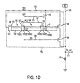
- FIG. 1D is a cross-sectional view of a 6 transistor (6T) pixel architecture partly in schematic diagram form showing a first charge barrier positioned between the first photo-diode and the second photo-diode and a second charge barrier positioned between the second photo-diode and the floating diffusion, according to an embodiment of the present invention.
- 6T 6 transistor
- FIG. 2 is a block diagram of a complementary metal oxide semiconductor (CMOS) imager architecture, according to an embodiment of the present invention.
- CMOS complementary metal oxide semiconductor
- FIG. 3A is a cross-sectional view of the pumped pixel architecture showing the charge barrier positioned between the first photo-diode and the second photo-diode and charge accumulated in the first photo-diode according to an embodiment of the present invention.
- FIG. 3D is a cross-sectional view of the pumped pixel architecture showing the charge barrier positioned between the first photo-diode and the second photo-diode and charge filling the clock well of the pump gate, according to an embodiment of the present invention.
- FIG. 3C is a cross-sectional view of the pumped pixel architecture showing the charge barrier positioned between the first photo-diode and the second photo-diode and a portion of the accumulated charge pumped over the charge barrier and into the second photo-diode, according to an embodiment of the present invention.
- FIG. 3D is a cross-sectional view of the pumped pixel architecture showing the charge barrier positioned between the first photo-diode and the second photo-diode and the remainder of the accumulated charge pumped over the charge harrier and into the second photo-diode, according to an embodiment of the present invention.
- FIG. 3E is a cross-sectional view of the pumped pixel architecture showing the charge barrier positioned between the first photo-diode and the second photo-diode and the accumulated charge transferred into the floating diffusion, according to an embodiment of the present invention.
- FIG. 3F is a cross-sectional view of the pumped pixel architecture showing the charge barrier positioned between the second photo-diode and the floating diffusion, according to an embodiment of the present invention.
- FIG. 3G is a cross-sectional view of the pumped pixel architecture showing a first charge harrier positioned between the first photo-diode and the second photo-diode, and a second charge barrier positioned between the second photo-diode and the floating diffusion, according to an embodiment of the present invention.
- the present invention provides a pumped pixel having dual photo-diodes (e.g. pinned photo-diodes) and at least one virtual charge barrier (e.g. a heavily p-doped region on the surface and an n-doped region underneath).
- One of the photo-diodes accumulates charge in response to impinging photons.
- the other photo-diode acts as a memory node that stores the accumulated charge.
- the accumulated charge is pumped (by a pump gate) over the charge barrier and into the photo-diode for storage or into the floating diffusion for readout.
- the charge barrier blocks the charge from leaking back into the photo-diode from where it was pumped. Being able to pump and store the charge may allow the imager to delay pixel readout and/or extend dynamic range without the need for large voltage differences (differences in well potentials) and/or doping between the photo-diode wells.
- FIG. 1A A six transistor (6T) circuit for a pixel 150 of a CMOS imager is illustrated in FIG. 1A .
- Pixel 150 is a 6T pixel, where 6T is used to designate the use of six transistors to operate a pixel.
- the 6T pixel 150 has photo-sensors such as exposed pinned photo-diode 162 , a shielded pinned photo-diode 164 , a reset transistor 184 , a transfer transistor 190 , a source follower transistor 186 , a row select transistor 188 , an anti-blooming gate 166 , a pump gate 167 and a charge harrier 165 .
- FIG. 1A shows the circuitry for operation of a single pixel 150 , and that in practical use, there may be an M.times.N array of pixels arranged in rows and columns with the pixels of the array accessed using row and column select circuitry, as described in more detail below.
- Photodiode 162 accumulates photo-electrons generated in response to impinging photons. This accumulated charge is pumped over charge barrier 165 and into pinned photo-diode 164 for storage when activated by the PG control signal during a storage period. The stored charge is then transferred to floating diffusion stage node A through transfer transistor 190 when activated by the TX control signal during a readout period.
- the source follower transistor 186 has a gate terminal connected to node A and thus amplifies the signal appearing at floating diffusion node A.
- Photodiode 162 accumulates a photo-generated charge in a doped region of the substrate (i.e. in a well). It is noted that the pixel 150 may include a photo-gate or other photon to charge converting device, in lieu of a pinned photodiode, as the initial accumulator for photo-generated charge.
- transfer transistor 190 is coupled to a transfer control signal line 191 for receiving the TX control signal, thereby serving to control the coupling of the photodiode 164 to node A.
- a voltage source Vpix is coupled through reset transistor 184 to node A.
- the gate terminal of reset transistor 184 is coupled to a reset control line 183 for receiving the RST control signal to control the reset operation in which the voltage source Vpix is connected to node A, pinned photo-diode 164 and pinned photo-diode 162 for clearing charge.
- a row select signal (RS) on a row select control line 160 is used to activate the row select transistor 188 .
- the row select control line 160 may be used to provide a row select signal (RS) to all of the pixels of the same row of the array, as are the RST and TX lines.
- Voltage source Vpix is coupled to transistors 184 and 186 by conductive line 195 .
- a column line 170 is coupled to all of the pixels of the same column of the array and typically has a current sink 176 at its lower end.
- the upper part of column line 170 outside of the pixel array, includes a pull-up circuit 111 which is used to selectively keep the voltage on column line 170 high.
- Maintaining a positive voltage on the column line 170 during an image acquisition phase of a pixel 150 keeps the potential in a known state on the column line 170 .
- Signals from the pixel 150 are therefore selectively coupled to a column readout circuit through the column line 170 and through a pixel output (“Pix_out”) line 177 coupled between the column line 170 and the column readout circuit.
- Pix_out line 177 is coupled to the sample and hold (S/H) column capacitors 114 and 116 (i.e. two capacitors per column line to perform correlated double sampling).
- Transistors 110 and 112 are also included to ensure that the pixel output signals (i.e. the potentials after reset and integration) are each stored on the appropriate capacitor. These two potentials are compared (i.e. subtracted from each other) to perform correlated double sampling.
- a value can be read from pixel 150 in a two step correlated double sampling process.
- node A and the photo-diodes 162 and 164 Prior to a charge integration period, node A and the photo-diodes 162 and 164 are reset to a high potential by activating reset transistor 184 , transfer transistor 190 and pump gate 167 .
- Photodiode 162 can alternatively be reset to a high potential by activating anti-blooming gate 166 .
- photodiode 162 produces a charge from incident light. This is also known as the image acquisition period. Charges may be transferred from photo-diode 162 to photo-diode 164 by activating pump gate 167 .
- node A and photo-diode 164 are reset to a high potential by activating reset transistor 184 and transfer transistor 190 to remove parasitic charges accumulated in photo-diode 164 due to mechanisms such as dark current and light leakage.
- node A is again reset to a high potential.
- the charge (i.e. reset signal) at node A after reset is readout to column line 170 via the source follower transistor 186 and row select transistor 188 .
- Readout circuitry 242 in FIG. 2 then samples and holds the reset signal on capacitor 116 .
- Transfer transistor 190 is then activated, and the charge from photodiode 164 is passed to node A, where the charge is amplified by source follower transistor 186 and passed to column line 170 through row select transistor 188 .
- Readout circuitry 242 then samples and holds the integrated charge signal on capacitor 114 .
- two different voltage signals are readout, sampled and held on capacitors 114 and 116 for further processing.
- all pixels in a row are readout simultaneously onto respective column lines 170 .
- FIG. 2 shows an example CMOS imager integrated circuit chip 201 that includes an array 230 of pixels and a controller 232 , which provides timing and control signals to enable reading out of signals stored in the pixels.
- Exemplary arrays have dimensions of M.times.N pixels, with the size of the array 230 depending on a particular application.
- the pixels in the array are reset, exposed to light and readout on a row by row basis (rolling shutter mode), or all the pixels in the array are simultaneously reset, exposed to light, and then readout row by row (global shutter mode). It is noted that the present invention may be utilized in either rolling shutter mode or global shutter mode to increase dynamic range and/or delay pixel readout.
- the pixel signals from the array 230 are read out a row at a time using a column parallel readout architecture.
- the controller 232 selects a particular row of pixels in the array 230 by controlling the operation of row addressing circuit 234 , row drivers 240 and column addressing circuit 244 .
- Signals corresponding to charges stored in the selected row of pixels and reset signals are provided on the column lines 170 to a column readout circuit 242 in the manner described above.
- the pixel signal read from each of the columns can be read out sequentially using a column addressing circuit 244 .
- Pixel signals (Vrst, Vsig) corresponding to the readout reset signal and integrated charge signal are provided as respective outputs Vout 1 , Vout 2 of the column readout circuit 242 where they are subtracted in differential amplifier 246 , digitized by analog to digital converter 248 , and sent to an image processor circuit 250 for image processing.
- FIG. 1B Shown in FIG. 1B is a cross sectional view of a pixel substrate shown in FIG. 1A .
- a substrate 130 may include pinned photo-diodes 162 and 164 separated by pump gate 167 and charge barrier 165 .
- the regions under the photodiodes, and the regions 151 , 153 (A), 153 (B) and 152 under the anti-bloom gate, pump gate and transfer gate respectively include charge wells for storing charge. It is noted that increasing the well potential lowers the well (makes the well deep for charge storage), whereas decreasing the well potential raises the well (makes the well shallow for blocking and/or transferring charge).
- pinned photo-diode 162 accumulates charge based on impinging photons. This accumulated charge is held in pinned photodiode 162 due to raised wells 151 and 153 (A).
- the well depths of the various gates may be modulated (raised or lowered) based on the voltage applied to the gate terminals (i.e., based on the voltage signal AB, PG and TX).
- anti-blooming gate 166 and pump gate 167 are driven by a negative voltage which raises the wells so that charge is isolated in pinned photo-diode 162 .
- the pump gate 167 is driven by a positive voltage to lower a clock barrier in region 153 (A) and a clock well in region 153 (B).
- the clock barrier and clock well are differently doped regions under the pump gate (e.g. the clock well is doped to be deeper than the dock barrier). This allows charge from pinned photo-diode 162 to transfer (i.e. spill over) into lowered clock well 153 (B).
- pump gate 167 is then driven by a negative voltage which raises clock barrier 153 (A) and clock well 153 (B) thereby transferring (i.e. pumping) the charge over the top of barrier 165 and into pinned photo-diode 164 for storage.
- the clock barrier due to being higher than the clock well, prevents charge stored in the clock well from spilling back into the first pinned photo-diode during the pumping process.
- transfer gate 190 is closed by applying a negative voltage therefore raising the transfer gate well and blocking charge from spilling into floating diffusion A.
- transfer gate 190 is pulsed with a high positive voltage which lowers the transfer gate well thereby transferring the stored charge from pinned photo-diode 164 and into floating diffusion A where the pixel readout procedure (described above) is performed.
- the substrate may be designed (i.e., doped) such that the wells in pinned photo-diode 162 and 164 have equivalent capacity.
- pump gate 167 is able to pump the charge from pinned photo-diode 162 over the charge barrier and into pinned photo-diode 164 regardless of the well depth of the photodiodes.
- the well capacity of pinned photo-diode 164 may be greater (i.e. deeper) than the well capacity of pinned photo-diode 162 .
- pump gate 167 may periodically (during the integration period) pump the accumulating charge into pinned photo-diode 164 (which has a deeper well than 162 ) thereby allowing a longer integration time where pinned photo-diode 162 accumulates with charge multiple times. It is noted that pump gate 167 may be modulated one time or multiple time during or after integration in order to pump the charge from pinned photo-diode 162 into pinned photo-diode 164 .
- clock well 153 may be designed to have the same capacity or smaller capacity than pinned photo-diode 162 in order to transfer the charge in a single pump or in multiple repeated pumps.
- anti-blooming gate 166 is optional. Anti-blooming gate 166 allows excess charge accumulated by pinned photo-diode 162 to spill over to potential Vpix rather than spilling over into adjacent pixels. Moreover, the anti-blooming gate 166 can be used to reset photo-diode 162 .
- the charge barrier may he positioned between other areas of the substrate.
- the charge barrier and pump gate are located between the second pinned photo-diode 164 and floating diffusion A (i.e. transfer gate and pump gate/barrier are swapped).
- accumulated charge in pinned photo-diode 162 may be transferred, over to pinned photo-diode 164 for storage during a storage period.
- the charge stored in pinned photo-diode 164 may he pumped over charge barrier 165 into floating, diffusion A.
- a transfer gate has a region 153 under the gate
- pump gate has regions 152 (A) and 152 (B) which are the clock barrier and clock well respectively.
- the pumped pixel may include two pump gates 167 and 190 , and two charge barriers 165 (A) and 165 (B) (i.e., there may be a pump gate and charge barrier between both pinned photo-diodes and between the pinned photo-diode and the floating diffusion).
- the first pump gate may include region 153 (A) and 153 (B) while the second pump gate may include regions 152 (A) and 152 (B) (i.e., the clock barriers and clock wells respectively).
- the charge barriers may be denoted as 165 (A) and 165 (B).
- the charge accumulated by pinned photo-diode 162 may be pumped over charge barrier 165 (A) and stored in pinned photo-diode 164 . Then, during a readout period, the charge stored in pinned photo-diode 164 may be pumped over charge barrier 165 B and into the floating diffusion A.
- the wells of the pinned photo-diode and the floating diffusion may be designed (i.e. doped) to be shallow or deep depending on the position of the pump gate.
- the wells for pinned photo-diode 162 , 164 and floating diffusion A may be all the same depth since there is a pump between the regions.
- the wells under pinned photo-diode 164 and floating diffusion A may be deeper than that of pinned photo-diode 162 in order to store more charge and increase dynamic range of the pixel.
- FIGS. 3A-3G Shown in FIGS. 3A-3G are cross sectional views of the pumped pixels showing the flow of charge at each stage during integration, storage and readout. The operation of the pixel in FIG. 1B is now described with respect of FIGS. 3A-3G .
- pump gate 167 and transfer gate 190 have negative voltage signals PG and TX thereby raising the dock barrier and clock well 390 and 392 and transfer well 394 .
- the first pinned photo-diode 162 is accumulating charge 302 . Since clock barrier 390 is raised, charge 302 is isolated in pinned photo-diode 162 .
- pump 167 voltage PG is increased to a positive voltage which lowers clock barrier 390 and clock well 392 .
- clock well 392 is lowered some or all of the charge (i.e., depending on the size of clock well 392 ) is transferred from the first pinned photo-diode 162 and into the clock well 392 as charge 304 (see FIG. 3B ).
- the pump gate 167 voltage PG is set to a negative voltage which raises clock harrier 390 and clock well 392 thereby pumping charge 304 over the top of the charge barrier and into the second pinned photo-diode 164 as charge 306 (see FIG. 3C ). Since the clock well is raised (i.e. doped differently) with respect to the clock well, charge in the clock well is blocked from spilling back into the first photo-diode during pumping.
- the pumping period may be repeated a plurality of times to pump all of charge 302 from the first pinned photo-diode 162 over the charge barrier and into the second pinned photo-diode 164 (charge 302 has been moved to 306 ).
- charge 306 is isolated in the second pinned photo-diode 164 due to the charge barrier and the raised transfer well 394 (see FIG. 3D ).
- transfer gate 190 may have its TX voltage increased to a positive voltage which lowers transfer well 394 allowing charge 306 to spill over (i.e., transfer) into floating diffusion A as charge 308 (see FIG. 3E ).
- the source follower transistor converts the charge to a voltage which is readout as pix_put 177 (see description of pixel readout as described above).
- the pump gate may be moved to different regions in the pumped pixel.
- the pump gate and charge barrier may be swapped with the transfer gate.
- transfer gate 167 and pump gate 190 may be biased with a negative voltage which raises their respective wells allowing charge to accumulate in first photodiode 162 .
- the voltage on transfer gate 167 may be increased to a positive voltage which lowers transfer well 394 allowing charge to spill over into second photodiode 164 for storage.
- the pump gate 190 may have its voltage increased to a positive voltage which lowers clock barrier 390 and clock well 392 to fill up with the charge from photodiode 164 .
- a negative voltage is then applied to pump gate 190 , the charge in clock well 392 will pour over the charge barrier 165 and into floating diffusion A as charge 320 .
- the pumping may be performed in a single pump or multiple pumps depending on the amount of charge.
- the transfer gate may be replaced with another pump gate (i.e., two pump gates may be utilized).
- pump gates 167 and 168 are held at negative voltages (i.e., their respective clock barriers and clock wells are raised therefore allowing charge to accumulate in photodiode 162 ).
- pump gate 167 voltage may be modulated (i.e., changed to a positive and negative voltage repeatedly) to pump the charge from pinned photo-diode 162 over charge barrier 165 (A) and into pinned photo-diode 164 as charge 306 .
- pump gate 168 voltage may be modulated (i.e., changed to a positive and negative voltage repeatedly) to pump the charge from pinned photo-diode 164 over charge harrier 165 (B) and into the floating diffusion A as charge 320 .
- the well capacities of the pinned photo-diodes, pump gates, transfer gates and floating diffusions may be designed (i.e., doped and biased) differently.
- the charge barrier 165 may be taller or shorter depending on the doping.
- the clock barrier and the clock well on the pump gate may be able to pump more or less charge depending on their relative difference with respect to each other.
- the imager may operate in a rolling shutter mode or a global shutter mode.
- three pointers may be employed (i.e., a reset pointer, a storage pointer and a read pointer).
- the reset pointer may traverse from the top to the bottom of the array performing a row by row pixel reset (i.e. the pinned photo-diodes, floating diffusions and gate wells for the pixels in each row are reset to a potential).
- Behind the reset pointer may be one of more storage pointers which may traverse from the top to the bottom of the array transferring (i.e., pumping) the charge accumulated in the photodiode into the second pinned photo-diodes for storage.
- Behind the storage pointer may be a read pointer which may also traverse from the top to the bottom of the pixel array to perform row by row charge transfer of the charge from the second pinned photo-diode into the floating diffusion for read out.
- a storage pointer is immediately positioned before the read pointer. Other storage pointers may also be positioned before the read pointer to increase dynamic range.
- the storage pointer may be beneficial in rolling shutter mode to control pixels to avoid large voltage swings and or to increase dynamic range.
- the first pinned photo-diode 162 may be controlled to accumulate charge repeatedly which is then periodically transferred over the barrier and stored (using the multiple storage pointers) in a second pinned photo-diode 164 .
- each pixel in every row is exposed during the integration period simultaneously, while the rows are still read out sequentially similar to the rolling shutter.
- a storage of each pixel value may be beneficial for delaying readout.
- the first pinned photo-diode 162 of every pixel may accumulate charge during the integration period and then have that charge pumped into the second pinned photo-diode 164 for storage. That stored charge may then be accessed (i.e., transferred into the floating diffusion) at a later time when the pixels are read out row by row, and while the first photo-diode 162 is accumulating charge for the next image.
- the present invention provides a pumped pixel which includes at least one pump gate and one charge barrier.
- charge is pumped over the charge barrier by modulating a clock barrier and clock well located below the pump gate.
- the combination of the pump gate and charge barrier in the pumped pixel allows for adjacent photodiodes to have similar well potentials while still being able to transfer charge (i.e., large well potential differences may be avoided).
Abstract
Description
Claims (13)
Priority Applications (1)
| Application Number | Priority Date | Filing Date | Title |
|---|---|---|---|
| US14/171,181 US9595560B2 (en) | 2011-03-25 | 2014-02-03 | Pumped pinned photodiode pixel array |
Applications Claiming Priority (3)
| Application Number | Priority Date | Filing Date | Title |
|---|---|---|---|
| US201161467561P | 2011-03-25 | 2011-03-25 | |
| US13/242,865 US8674282B2 (en) | 2011-03-25 | 2011-09-23 | Pumped pinned photodiode pixel array |
| US14/171,181 US9595560B2 (en) | 2011-03-25 | 2014-02-03 | Pumped pinned photodiode pixel array |
Related Parent Applications (1)
| Application Number | Title | Priority Date | Filing Date |
|---|---|---|---|
| US13/242,865 Division US8674282B2 (en) | 2011-03-25 | 2011-09-23 | Pumped pinned photodiode pixel array |
Publications (2)
| Publication Number | Publication Date |
|---|---|
| US20140146209A1 US20140146209A1 (en) | 2014-05-29 |
| US9595560B2 true US9595560B2 (en) | 2017-03-14 |
Family
ID=46876520
Family Applications (2)
| Application Number | Title | Priority Date | Filing Date |
|---|---|---|---|
| US13/242,865 Active 2032-07-17 US8674282B2 (en) | 2011-03-25 | 2011-09-23 | Pumped pinned photodiode pixel array |
| US14/171,181 Active 2032-01-28 US9595560B2 (en) | 2011-03-25 | 2014-02-03 | Pumped pinned photodiode pixel array |
Family Applications Before (1)
| Application Number | Title | Priority Date | Filing Date |
|---|---|---|---|
| US13/242,865 Active 2032-07-17 US8674282B2 (en) | 2011-03-25 | 2011-09-23 | Pumped pinned photodiode pixel array |
Country Status (1)
| Country | Link |
|---|---|
| US (2) | US8674282B2 (en) |
Families Citing this family (36)
| Publication number | Priority date | Publication date | Assignee | Title |
|---|---|---|---|---|
| US8809913B2 (en) * | 2012-11-07 | 2014-08-19 | Semiconductor Components Industries, Llc | Pixel architecture and method |
| JP6021613B2 (en) * | 2012-11-29 | 2016-11-09 | キヤノン株式会社 | Imaging device, imaging apparatus, and imaging system |
| US9462202B2 (en) * | 2013-06-06 | 2016-10-04 | Samsung Electronics Co., Ltd. | Pixel arrays and imaging devices with reduced blooming, controllers and methods |
| US9578223B2 (en) | 2013-08-21 | 2017-02-21 | Qualcomm Incorporated | System and method for capturing images with multiple image sensing elements |
| GB2537421A (en) * | 2015-04-17 | 2016-10-19 | Stmicroelectronics (Research & Development) Ltd | A pixel having a plurality of photodiodes |
| US9942503B2 (en) * | 2016-02-23 | 2018-04-10 | Semiconductor Components Industries, Llc | Image sensors having high-efficiency charge storage capabilities |
| US9933300B2 (en) * | 2016-02-23 | 2018-04-03 | BAE Systems Imaging Solutions Inc. | Ultra-high dynamic range two photodiode pixel architecture |
| US9843754B1 (en) | 2016-06-14 | 2017-12-12 | Omnivision Technologies, Inc. | Global shutter pixel with hybrid transfer storage gate-storage diode storage node |
| US9848148B1 (en) * | 2016-06-17 | 2017-12-19 | Semiconductor Components Industries, Llc | Methods and apparatus for a multiple storage pixel imaging system |
| US10917625B1 (en) | 2016-10-20 | 2021-02-09 | Facebook Technologies, Llc | Time multiplexed dual-band sensor |
| US10192911B2 (en) | 2017-05-09 | 2019-01-29 | Apple Inc. | Hybrid image sensors with improved charge injection efficiency |
| US10419701B2 (en) | 2017-06-26 | 2019-09-17 | Facebook Technologies, Llc | Digital pixel image sensor |
| US10686996B2 (en) | 2017-06-26 | 2020-06-16 | Facebook Technologies, Llc | Digital pixel with extended dynamic range |
| US10598546B2 (en) | 2017-08-17 | 2020-03-24 | Facebook Technologies, Llc | Detecting high intensity light in photo sensor |
| US11393867B2 (en) | 2017-12-06 | 2022-07-19 | Facebook Technologies, Llc | Multi-photodiode pixel cell |
| US10969273B2 (en) | 2018-03-19 | 2021-04-06 | Facebook Technologies, Llc | Analog-to-digital converter having programmable quantization resolution |
| US11004881B2 (en) | 2018-04-03 | 2021-05-11 | Facebook Technologies, Llc | Global shutter image sensor |
| US10923523B2 (en) * | 2018-04-16 | 2021-02-16 | Facebook Technologies, Llc | Multi-photodiode pixel cell |
| US11233085B2 (en) | 2018-05-09 | 2022-01-25 | Facebook Technologies, Llc | Multi-photo pixel cell having vertical gate structure |
| JP2019204841A (en) * | 2018-05-22 | 2019-11-28 | 株式会社村田製作所 | Semiconductor device |
| US11089241B2 (en) | 2018-06-11 | 2021-08-10 | Facebook Technologies, Llc | Pixel cell with multiple photodiodes |
| US11906353B2 (en) | 2018-06-11 | 2024-02-20 | Meta Platforms Technologies, Llc | Digital pixel with extended dynamic range |
| US11089210B2 (en) | 2018-06-11 | 2021-08-10 | Facebook Technologies, Llc | Configurable image sensor |
| US11463636B2 (en) | 2018-06-27 | 2022-10-04 | Facebook Technologies, Llc | Pixel sensor having multiple photodiodes |
| US10897586B2 (en) | 2018-06-28 | 2021-01-19 | Facebook Technologies, Llc | Global shutter image sensor |
| US11956413B2 (en) | 2018-08-27 | 2024-04-09 | Meta Platforms Technologies, Llc | Pixel sensor having multiple photodiodes and shared comparator |
| US11595602B2 (en) | 2018-11-05 | 2023-02-28 | Meta Platforms Technologies, Llc | Image sensor post processing |
| US20210327952A1 (en) * | 2018-11-21 | 2021-10-21 | BAE Systems Imaging Solutions Inc. | Time delay integration structure for complementary metal-oxide semiconductor imaging sensor |
| US11102430B2 (en) | 2018-12-10 | 2021-08-24 | Facebook Technologies, Llc | Pixel sensor having multiple photodiodes |
| US11218660B1 (en) | 2019-03-26 | 2022-01-04 | Facebook Technologies, Llc | Pixel sensor having shared readout structure |
| US11943561B2 (en) | 2019-06-13 | 2024-03-26 | Meta Platforms Technologies, Llc | Non-linear quantization at pixel sensor |
| US11496703B2 (en) | 2019-07-25 | 2022-11-08 | Trustees Of Dartmouth College | High conversion gain and high fill-factor image sensors with pump-gate and vertical charge storage well for global-shutter and high-speed applications |
| US11936998B1 (en) | 2019-10-17 | 2024-03-19 | Meta Platforms Technologies, Llc | Digital pixel sensor having extended dynamic range |
| US11902685B1 (en) | 2020-04-28 | 2024-02-13 | Meta Platforms Technologies, Llc | Pixel sensor having hierarchical memory |
| US11910114B2 (en) | 2020-07-17 | 2024-02-20 | Meta Platforms Technologies, Llc | Multi-mode image sensor |
| US11956560B2 (en) | 2020-10-09 | 2024-04-09 | Meta Platforms Technologies, Llc | Digital pixel sensor having reduced quantization operation |
Citations (5)
| Publication number | Priority date | Publication date | Assignee | Title |
|---|---|---|---|---|
| US20060145203A1 (en) * | 2004-12-30 | 2006-07-06 | Zeynep Toros | Method and apparatus for controlling charge transfer in CMOS sensors with an implant by the transfer gate |
| US20060261246A1 (en) * | 2005-05-18 | 2006-11-23 | Alexander Krymski | Pixel circuit for image sensor |
| US20090050943A1 (en) * | 2007-08-23 | 2009-02-26 | Micron Technology, Inc. | Imagers, apparatuses and systems utilizing pixels with improved optical resolution and methods of operating the same |
| WO2009125821A1 (en) * | 2008-04-09 | 2009-10-15 | Canon Kabushiki Kaisha | Solid-state imaging apparatus and driving method thereof |
| US8723284B1 (en) * | 2011-02-02 | 2014-05-13 | Aptina Imaging Corporation | Back side illuminated CMOS image sensor with global shutter storage gates stacked on top of pinned photodiodes |
-
2011
- 2011-09-23 US US13/242,865 patent/US8674282B2/en active Active
-
2014
- 2014-02-03 US US14/171,181 patent/US9595560B2/en active Active
Patent Citations (5)
| Publication number | Priority date | Publication date | Assignee | Title |
|---|---|---|---|---|
| US20060145203A1 (en) * | 2004-12-30 | 2006-07-06 | Zeynep Toros | Method and apparatus for controlling charge transfer in CMOS sensors with an implant by the transfer gate |
| US20060261246A1 (en) * | 2005-05-18 | 2006-11-23 | Alexander Krymski | Pixel circuit for image sensor |
| US20090050943A1 (en) * | 2007-08-23 | 2009-02-26 | Micron Technology, Inc. | Imagers, apparatuses and systems utilizing pixels with improved optical resolution and methods of operating the same |
| WO2009125821A1 (en) * | 2008-04-09 | 2009-10-15 | Canon Kabushiki Kaisha | Solid-state imaging apparatus and driving method thereof |
| US8723284B1 (en) * | 2011-02-02 | 2014-05-13 | Aptina Imaging Corporation | Back side illuminated CMOS image sensor with global shutter storage gates stacked on top of pinned photodiodes |
Also Published As
| Publication number | Publication date |
|---|---|
| US20140146209A1 (en) | 2014-05-29 |
| US8674282B2 (en) | 2014-03-18 |
| US20120241591A1 (en) | 2012-09-27 |
Similar Documents
| Publication | Publication Date | Title |
|---|---|---|
| US9595560B2 (en) | Pumped pinned photodiode pixel array | |
| US10587830B2 (en) | Method for controlling an active pixel image sensor | |
| US10965893B2 (en) | Solid-state imaging device, method of driving the same, and electronic apparatus | |
| US9496304B2 (en) | Image sensor pixel cell with switched deep trench isolation structure | |
| US10483304B2 (en) | Image sensor | |
| US9054007B2 (en) | Image sensor pixel cell with switched deep trench isolation structure | |
| US8698061B2 (en) | Image sensors, methods, and pixels with storage and transfer gates | |
| US7969494B2 (en) | Imager and system utilizing pixel with internal reset control and method of operating same | |
| US9654713B2 (en) | Image sensors, methods, and pixels with tri-level biased transfer gates | |
| US9455295B2 (en) | Solid-state image sensor with MOS capacitor storage section to which a negative bias is applied after a reset sampling period and electronic device incorporating same | |
| US20160276380A1 (en) | Photosensitive capacitor pixel for image sensor | |
| JP2010182887A (en) | Solid-state imaging device, method of manufacturing solid-state imaging device, method of driving solid-state imaging device, and electronic apparatus | |
| US11348956B2 (en) | Multi-gate lateral overflow integration capacitor sensor | |
| EP2648404A1 (en) | Floating diffusion pre-charge | |
| EP3461119A1 (en) | Pixel to pixel copier systems and methods | |
| US20200350350A1 (en) | Image sensors, methods, and pixels with floating diffusion and gate for charge storage | |
| US20200304743A1 (en) | Hybrid image sensors with improved charge injection efficiency | |
| US11812175B2 (en) | Image sensor and method of operating the same | |
| US9472587B2 (en) | Storage transistor with optical isolation |
Legal Events
| Date | Code | Title | Description |
|---|---|---|---|
| AS | Assignment |
Owner name: APTINA IMAGING CORPORATION, CAYMAN ISLANDS Free format text: ASSIGNMENT OF ASSIGNORS INTEREST;ASSIGNORS:WAN, CHUNG CHUN;LI, XIANGLI;SIGNING DATES FROM 20110912 TO 20110919;REEL/FRAME:034488/0651 |
|
| AS | Assignment |
Owner name: SEMICONDUCTOR COMPONENTS INDUSTRIES, LLC, ARIZONA Free format text: ASSIGNMENT OF ASSIGNORS INTEREST;ASSIGNOR:APTINA IMAGING CORPORATION;REEL/FRAME:034673/0001 Effective date: 20141217 |
|
| AS | Assignment |
Owner name: DEUTSCHE BANK AG NEW YORK BRANCH, NEW YORK Free format text: SECURITY INTEREST;ASSIGNOR:SEMICONDUCTOR COMPONENTS INDUSTRIES, LLC;REEL/FRAME:038620/0087 Effective date: 20160415 |
|
| AS | Assignment |
Owner name: DEUTSCHE BANK AG NEW YORK BRANCH, AS COLLATERAL AG Free format text: CORRECTIVE ASSIGNMENT TO CORRECT THE INCORRECT PATENT NUMBER 5859768 AND TO RECITE COLLATERAL AGENT ROLE OF RECEIVING PARTY IN THE SECURITY INTEREST PREVIOUSLY RECORDED ON REEL 038620 FRAME 0087. ASSIGNOR(S) HEREBY CONFIRMS THE SECURITY INTEREST;ASSIGNOR:SEMICONDUCTOR COMPONENTS INDUSTRIES, LLC;REEL/FRAME:039853/0001 Effective date: 20160415 Owner name: DEUTSCHE BANK AG NEW YORK BRANCH, AS COLLATERAL AGENT, NEW YORK Free format text: CORRECTIVE ASSIGNMENT TO CORRECT THE INCORRECT PATENT NUMBER 5859768 AND TO RECITE COLLATERAL AGENT ROLE OF RECEIVING PARTY IN THE SECURITY INTEREST PREVIOUSLY RECORDED ON REEL 038620 FRAME 0087. ASSIGNOR(S) HEREBY CONFIRMS THE SECURITY INTEREST;ASSIGNOR:SEMICONDUCTOR COMPONENTS INDUSTRIES, LLC;REEL/FRAME:039853/0001 Effective date: 20160415 |
|
| STCF | Information on status: patent grant |
Free format text: PATENTED CASE |
|
| MAFP | Maintenance fee payment |
Free format text: PAYMENT OF MAINTENANCE FEE, 4TH YEAR, LARGE ENTITY (ORIGINAL EVENT CODE: M1551); ENTITY STATUS OF PATENT OWNER: LARGE ENTITY Year of fee payment: 4 |
|
| AS | Assignment |
Owner name: FAIRCHILD SEMICONDUCTOR CORPORATION, ARIZONA Free format text: RELEASE OF SECURITY INTEREST IN PATENTS RECORDED AT REEL 038620, FRAME 0087;ASSIGNOR:DEUTSCHE BANK AG NEW YORK BRANCH, AS COLLATERAL AGENT;REEL/FRAME:064070/0001 Effective date: 20230622 Owner name: SEMICONDUCTOR COMPONENTS INDUSTRIES, LLC, ARIZONA Free format text: RELEASE OF SECURITY INTEREST IN PATENTS RECORDED AT REEL 038620, FRAME 0087;ASSIGNOR:DEUTSCHE BANK AG NEW YORK BRANCH, AS COLLATERAL AGENT;REEL/FRAME:064070/0001 Effective date: 20230622 |