US9595420B2 - Method for preparing lamella - Google Patents
Method for preparing lamella Download PDFInfo
- Publication number
- US9595420B2 US9595420B2 US13/706,426 US201213706426A US9595420B2 US 9595420 B2 US9595420 B2 US 9595420B2 US 201213706426 A US201213706426 A US 201213706426A US 9595420 B2 US9595420 B2 US 9595420B2
- Authority
- US
- United States
- Prior art keywords
- lamella
- measurement region
- thickness
- charged particles
- electron beam
- Prior art date
- Legal status (The legal status is an assumption and is not a legal conclusion. Google has not performed a legal analysis and makes no representation as to the accuracy of the status listed.)
- Active
Links
Images


Classifications
-
- H—ELECTRICITY
- H01—ELECTRIC ELEMENTS
- H01J—ELECTRIC DISCHARGE TUBES OR DISCHARGE LAMPS
- H01J37/00—Discharge tubes with provision for introducing objects or material to be exposed to the discharge, e.g. for the purpose of examination or processing thereof
- H01J37/26—Electron or ion microscopes; Electron or ion diffraction tubes
- H01J37/261—Details
-
- H—ELECTRICITY
- H01—ELECTRIC ELEMENTS
- H01J—ELECTRIC DISCHARGE TUBES OR DISCHARGE LAMPS
- H01J37/00—Discharge tubes with provision for introducing objects or material to be exposed to the discharge, e.g. for the purpose of examination or processing thereof
- H01J37/30—Electron-beam or ion-beam tubes for localised treatment of objects
- H01J37/304—Controlling tubes by information coming from the objects or from the beam, e.g. correction signals
-
- G—PHYSICS
- G01—MEASURING; TESTING
- G01N—INVESTIGATING OR ANALYSING MATERIALS BY DETERMINING THEIR CHEMICAL OR PHYSICAL PROPERTIES
- G01N1/00—Sampling; Preparing specimens for investigation
- G01N1/28—Preparing specimens for investigation including physical details of (bio-)chemical methods covered elsewhere, e.g. G01N33/50, C12Q
- G01N1/286—Preparing specimens for investigation including physical details of (bio-)chemical methods covered elsewhere, e.g. G01N33/50, C12Q involving mechanical work, e.g. chopping, disintegrating, compacting, homogenising
-
- G—PHYSICS
- G01—MEASURING; TESTING
- G01N—INVESTIGATING OR ANALYSING MATERIALS BY DETERMINING THEIR CHEMICAL OR PHYSICAL PROPERTIES
- G01N23/00—Investigating or analysing materials by the use of wave or particle radiation, e.g. X-rays or neutrons, not covered by groups G01N3/00 – G01N17/00, G01N21/00 or G01N22/00
- G01N23/22—Investigating or analysing materials by the use of wave or particle radiation, e.g. X-rays or neutrons, not covered by groups G01N3/00 – G01N17/00, G01N21/00 or G01N22/00 by measuring secondary emission from the material
- G01N23/225—Investigating or analysing materials by the use of wave or particle radiation, e.g. X-rays or neutrons, not covered by groups G01N3/00 – G01N17/00, G01N21/00 or G01N22/00 by measuring secondary emission from the material using electron or ion
- G01N23/2251—Investigating or analysing materials by the use of wave or particle radiation, e.g. X-rays or neutrons, not covered by groups G01N3/00 – G01N17/00, G01N21/00 or G01N22/00 by measuring secondary emission from the material using electron or ion using incident electron beams, e.g. scanning electron microscopy [SEM]
-
- H—ELECTRICITY
- H01—ELECTRIC ELEMENTS
- H01J—ELECTRIC DISCHARGE TUBES OR DISCHARGE LAMPS
- H01J2237/00—Discharge tubes exposing object to beam, e.g. for analysis treatment, etching, imaging
- H01J2237/20—Positioning, supporting, modifying or maintaining the physical state of objects being observed or treated
- H01J2237/202—Movement
- H01J2237/20207—Tilt
-
- H—ELECTRICITY
- H01—ELECTRIC ELEMENTS
- H01J—ELECTRIC DISCHARGE TUBES OR DISCHARGE LAMPS
- H01J2237/00—Discharge tubes exposing object to beam, e.g. for analysis treatment, etching, imaging
- H01J2237/30—Electron or ion beam tubes for processing objects
- H01J2237/317—Processing objects on a microscale
- H01J2237/3174—Etching microareas
- H01J2237/31745—Etching microareas for preparing specimen to be viewed in microscopes or analyzed in microanalysers
-
- H—ELECTRICITY
- H01—ELECTRIC ELEMENTS
- H01J—ELECTRIC DISCHARGE TUBES OR DISCHARGE LAMPS
- H01J2237/00—Discharge tubes exposing object to beam, e.g. for analysis treatment, etching, imaging
- H01J2237/30—Electron or ion beam tubes for processing objects
- H01J2237/317—Processing objects on a microscale
- H01J2237/31749—Focused ion beam
-
- H—ELECTRICITY
- H01—ELECTRIC ELEMENTS
- H01J—ELECTRIC DISCHARGE TUBES OR DISCHARGE LAMPS
- H01J37/00—Discharge tubes with provision for introducing objects or material to be exposed to the discharge, e.g. for the purpose of examination or processing thereof
- H01J37/02—Details
- H01J37/20—Means for supporting or positioning the object or the material; Means for adjusting diaphragms or lenses associated with the support
-
- H—ELECTRICITY
- H01—ELECTRIC ELEMENTS
- H01J—ELECTRIC DISCHARGE TUBES OR DISCHARGE LAMPS
- H01J37/00—Discharge tubes with provision for introducing objects or material to be exposed to the discharge, e.g. for the purpose of examination or processing thereof
- H01J37/26—Electron or ion microscopes; Electron or ion diffraction tubes
- H01J37/28—Electron or ion microscopes; Electron or ion diffraction tubes with scanning beams
Definitions
- the present invention relates to a lamella preparation method and a lamella preparation apparatus for preparing a lamella by etching processing using a focused ion beam.
- TEM observation is known as a method of observing a microscopic region in a sample for the purpose of analyzing a defect in a semiconductor device or the like.
- TEM observation in order to obtain a transmission electron image, as preprocessing, it is necessary to process a sample into a lamella having a thickness through which an electron beam may transmit.
- a lamella preparation method using a focused ion beam is used as a method of preparing a lamella.
- etching processing of peripheral portions of a sample is performed so as to leave a portion in the sample including a region of which observation is desired.
- etching processing of the remaining portion is performed until the portion has a thickness through which an electron beam may transmit to prepare the lamella. This enables preparation of a lamella precisely including the region of which the observation is desired.
- the thickness be uniform throughout the lamella.
- the nonuniformity affects a TEM image and information of the defect and the effect of the nonuniformity in thickness cannot be separated, which causes the analysis to be difficult.
- a focused ion beam has a certain beam density distribution due to the nature thereof, and thus, when a lamella is prepared by irradiating a focused ion beam from a surface side of a sample, the lamella is tapered, which means the thickness of the lamella is nonuniform.
- a method for solving such a problem there is disclosed a method of preparing a lamella having a vertical thin wall by etching processing with the sample being slanted taking into consideration the beam density distribution of the focused ion beam (see Japanese Patent Application Laid-open No. Hei 4-76437). According to this method, a lamella having a uniform thickness irrespective of the beam density distribution of the focused ion beam may be prepared.
- the present invention has been made in view of the above-mentioned circumstances, and the present invention provides a lamella preparation apparatus and a lamella preparation method capable of preparing a lamella having a uniform thickness without depending on the skill of an operator.
- a lamella preparation apparatus for preparing a lamella by performing processing of a sample using a focused ion beam irradiated from a focused ion beam column
- the lamella preparation apparatus including: a sample stage for mounting the lamella thereon; an electron beam column for irradiating an electron beam onto the lamella; a charged particle detector for detecting charged particles released from the lamella by irradiation of the electron beam; and a display unit for displaying an observation image of the lamella formed using a detection signal from the charged particle detector.
- the lamella preparation apparatus further includes: an input unit for setting a first measurement region on an upper side and a second measurement region on a lower side of the lamella in the observation image; and a slant angle calculating unit for calculating a slant angle of the lamella from a detected amount of the charged particles generated from the first measurement region and a detected amount of the charged particles generated from the second measurement region by irradiation of the electron beam and a distance between the first measurement region and the second measurement region.
- a lamella preparation method of preparing a lamella by performing processing of a sample using a focused ion beam including: irradiating an electron beam onto the lamella to form an observation image; setting a first measurement region on an upper side and a second measurement region on a lower side of the lamella in the observation image; irradiating the electron beam onto the first measurement region and the second measurement region and detecting charged particles generated there from; calculating a slant angle of the lamella from a detected amount of the charged particles generating from the first measurement region, a detected amount of the charged particles generated from the second measurement region, and a distance between the first measurement region and the second measurement region; slanting the lamella with respect to the focused ion beam by the calculated slant angle; and irradiating the focused ion beam onto the lamella to perform finish processing.
- the present invention has an action and effect that the slant angle may be estimated, in particular, even when the slant angle of the lamella is small and a beam is irradiated from a direction perpendicular to a surface of the sample, that is, from a direction within an observation surface of the lamella, and thus, it is difficult to measure the slant angle from the obtained observation image.
- a lamella having a uniform thickness may be prepared without depending on the skill of an operator.
- FIG. 1 is a view illustrating the configuration of a lamella preparation apparatus according to an embodiment of the present invention
- FIG. 2A is an explanatory diagram of lamella preparation according to the embodiment of the present invention.
- FIG. 2B is an enlarged view of a vicinity of a lamella
- FIG. 2C is another enlarged view of the vicinity of the lamella
- FIG. 3A is a cross-sectional view of the lamella according to the embodiment of the present invention.
- FIG. 3B is another cross-sectional view of the lamella according to the embodiment of the present invention.
- FIG. 4 is a flow chart illustrating a lamella preparation method according to the embodiment of the present invention.
- FIG. 5A is an explanatory diagram of lamella preparation according to the embodiment of the present invention.
- FIG. 5B is a SEM image of an observation surface
- FIG. 6 is a graph showing the relationship between the film thickness and the amount of reflected electrons according to the embodiment of the present invention.
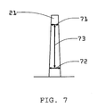
- FIG. 7 is a cross-sectional view of the lamella according to the embodiment of the present invention.
- FIG. 8A is an explanatory diagram of a taper angle according to the embodiment of the present invention.
- FIG. 8B is an explanatory diagram of finish processing.
- a lamella preparation apparatus and a lamella preparation method according to an embodiment of the present invention are described in the following.
- the lamella preparation apparatus of this embodiment includes an EB column 1 , an FIB column 2 , and a sample chamber 3 .
- An electron beam 8 from the EB column 1 and an ion beam 9 from the FIB column 2 may be irradiated onto a sample 7 housed in the sample chamber 3 .
- the lamella preparation apparatus further includes a secondary electron detector 4 and a reflected electron detector 5 as charged particle detectors.
- the secondary electron detector 4 may detect secondary electrons generated from the sample 7 by irradiation of the electron beam 8 or the ion beam 9 .
- the reflected electron detector 5 is provided in the EB column 1 .
- the reflected electron detector 5 may detect electrons reflected by the sample 7 as a result of irradiation of the electron beam 8 onto the sample 7 .
- the lamella preparation apparatus further includes a sample stage 6 for mounting the sample 7 thereon. By slanting the sample stage 6 , the incident angle of the ion beam 9 on the sample 7 may be changed.
- the sample stage 6 is controlled by a sample stage control unit 16 .
- the lamella preparation apparatus further includes an EB control unit 12 , an FIB control unit 13 , an image formation unit 14 , and a display unit 17 .
- the EB control unit 12 controls irradiation of the electron beam 8 from the EB column 1 .
- the FIB control unit 13 controls irradiation of the ion beam 9 from the FIB column 2 .
- the image formation unit 14 forms a reflected electron image from a signal for scanning the electron beam 8 of the EB control unit 12 and a signal of reflected electrons detected by the reflected electron detector 5 .
- the display unit 17 may display the reflected electron image.
- the image formation unit 14 forms a SEM image from the signal for scanning the electron beam 8 of the EB control unit 12 and a signal of secondary electrons detected by the secondary electron detector 4 .
- the display unit 17 may display the SEM image.
- the image formation unit 14 forms a SIM image from a signal for scanning the ion beam 9 of the FIB control unit 13 and the signal of secondary electrons detected by the secondary electron detector 4 .
- the display unit 17 may display the SIM image.
- the lamella preparation apparatus further includes an input unit 10 and a control unit 11 .
- An operator inputs to the input unit 10 conditions with regard to control of the apparatus.
- the input unit 10 sends input information to the control unit 11 .
- the control unit 11 sends a control signal to the EB control unit 12 , the FIB control unit 13 , the image formation unit 14 , the sample stage control unit 16 , or the display unit 17 to control the apparatus.
- an operator sets an irradiation region of the ion beam 9 based on, for example, an observation image such as a reflected electron image, a SEM image, or a SIM image displayed on the display unit 17 .
- An operator inputs using the input unit 10 a processing frame for setting the irradiation region on the observation image displayed on the display unit 17 .
- an operator inputs an instruction to start processing to the input unit 10 .
- a signal for indicating the irradiation region and a signal for starting processing are sent from the control unit 11 to the FIB control unit 13 , and the ion beam 9 is irradiated from the FIB control unit 13 onto the specified irradiation region of the sample 7 . This enables irradiation of the ion beam 9 onto the irradiation region specified by the operator.
- the lamella preparation apparatus of this embodiment may prepare a lamella 21 by performing processing of a part of the sample 7 using the ion beam 9 .
- FIG. 2B is an enlarged view of the vicinity of the lamella.
- the ion beam 9 is irradiated onto the sample 7 to form a processing groove 22 so as to leave the lamella 21 .
- the lamella 21 has a thickness through which the electron beam 8 does not transmit.
- FIG. 2C by performing thinning processing of the lamella 21 using the ion beam 9 , the lamella 21 may have a thickness through which the electron beam 8 may transmit.
- a portion 23 which does not undergo the thinning processing has a thickness through which the electron beam 8 cannot transmit.
- the lamella 21 having a thickness through which the electron beam 8 may transmit and a portion having a thickness through which the electron beam 8 cannot transmit may be formed in a part of the sample 7 .
- the lamella 21 formed by the thinning processing using the ion beam 9 has a small thickness 21 b on an upper side which is the FIB column 2 side of the lamella 21 (on a distal end side of the lamella 21 ) and a large thickness 21 c on a lower side which is the sample stage 6 side (on a proximal end side of the lamella 21 ).
- the reason for this is that the current density of the ion beam 9 has a Gaussian distribution, which affects the lamella 21 processed using the ion beam 9 to taper the lamella 21 .
- the thickness of the lamella 21 which is the target of the observation is desired to be uniform. Therefore, the sample stage 6 is slanted with respect to the ion beam 9 so as to prevent a tapered shape.
- the lamella 31 may have a reversed tapered shape in which a thickness 31 b on the upper side is large and a thickness 31 c on the lower side is small.
- the slant angle of the tapered shape that is, the slant angle of the lamella 21 is one degree or smaller, which is extremely small. Therefore, it is difficult to recognize the slant angle, and thus, conventionally, it follows that operation for slanting the sample stage 6 to adjust the angle of irradiation of the ion beam depends on the skill of an operator.
- the lamella preparation apparatus of this embodiment includes a calculation unit 15 for calculating an optimum slant angle of the sample stage 6 , and thus, even when the slant angle is one degree or smaller, the sample stage 6 may be slanted to form an optimum slant angle and the lamella 21 having a uniform thickness may be prepared.
- FIG. 4 is a flow chart illustrating a lamella preparation method of this embodiment.
- the electron beam 8 is irradiated onto the lamella 21 formed by the thinning processing, and reflected electrons generated from a measurement region of the lamella 21 are detected (S 1 ).
- the slant angle of the sample stage 6 is calculated (S 2 ).
- the sample stage 6 is slanted so that the slant angle becomes a calculated angle (S 3 ).
- the ion beam 9 is irradiated onto the lamella 21 to perform finish processing (S 4 ). In this way, the lamella 21 having a uniform thickness may be prepared.
- the lamella preparation apparatus of this embodiment reflected electrons are detected as follows. As illustrated in FIG. 5A , the lamella 21 having a thickness through which the electron beam 8 may transmit and a portion having a thickness through which the electron beam 8 cannot transmit are formed in a part of the sample 7 .
- the sample stage 6 is located so that the ion beam 9 is vertically incident on the surface of the sample 7 . Further, the sample 7 is located so that the electron beam 8 may scan and irradiate an observation surface 21 a of the lamella 21 .
- FIG. 5B is a SEM image obtained by scanning and irradiation of the observation surface 21 a using the electron beam 8 .
- An operator sets measurement regions 41 and 42 on the upper side and the lower side, respectively, of the observation surface 21 a based on the SEM image. As shown, the measurement regions 41 , 42 are set on the observation surface 21 a at locations where the lamella has a thickness through which the electron beam 8 may transmit. Stated otherwise, the measurement regions 41 , 42 are located where the lamella is thin enough to transmit therethrough the electron beam 8 . Further, an operator sets a reference region 43 in the portion 23 which does not undergo the thinning processing. Then, the electron beam 8 is irradiated onto the measurement regions 41 and 42 and the reference region 43 and reflected electrons are detected.
- FIG. 6 is a graph showing the relationship between the film thickness and the amount of reflected electrons.
- a horizontal axis 61 denotes the film thickness while a vertical axis 62 denotes the amount of reflected electrons measured in the measurement region.
- an amount of reflected electrons 63 almost does not change even when the film thickness changes.
- an amount of reflected electrons 64 becomes smaller. The reason is that, when the film thickness is small, an amount of electrons which transmit through the lamella 21 of the electron beam 8 irradiated onto the measurement region increases and the amount of reflected electrons decreases.
- the lamella preparation apparatus of this embodiment irradiates the electron beam 8 onto the measurement regions 41 and 42 and measures the amount of reflected electrons generated from each of the regions.
- the amount of reflected electrons depends on an amount of the irradiated electron beam 8 , and the current amount of the electron beam 8 may fluctuate every time the measurement is made. Therefore, in order to make an accurate measurement, the electron beam 8 is irradiated onto the measurement regions 41 and 42 and the reference region 43 , and the amounts of reflected electrons in the measurement regions 41 and 42 , respectively, are divided by the amount of reflected electrons in the reference region 43 having a thickness through which the electron beam 8 does not transmit. By using such figures, the measurement of the amounts of reflected electrons may be free from the effect of fluctuations in the amount of the irradiated electron beam 8 .
- the thicknesses of the measurement regions 41 and 42 may be estimated.
- FIG. 7 is a cross-sectional view of the lamella 21 .
- the amount of reflected electrons in the measurement region 41 and the amount of reflected electrons in the measurement region 42 are the same.
- the lamella 21 has a tapered shape as illustrated in FIG. 7 , the amount of reflected electrons in the measurement region 41 is smaller than the amount of reflected electrons in the measurement region 42 . From this difference and a distance 73 between the measurement region 41 and the measurement region 42 , the taper angle which is the slant angle of the lamella 21 may be calculated.
- ⁇ 0.47 degrees.
- one surface of the lamella 21 may be set to be in parallel with the ion beam 9 .
- the lamella 21 having a uniform thickness may be prepared.
Landscapes
- Chemical & Material Sciences (AREA)
- Analytical Chemistry (AREA)
- Physics & Mathematics (AREA)
- Health & Medical Sciences (AREA)
- Life Sciences & Earth Sciences (AREA)
- Biochemistry (AREA)
- General Health & Medical Sciences (AREA)
- General Physics & Mathematics (AREA)
- Immunology (AREA)
- Pathology (AREA)
- Sampling And Sample Adjustment (AREA)
- Analysing Materials By The Use Of Radiation (AREA)
Abstract
Description
Claims (11)
Applications Claiming Priority (2)
| Application Number | Priority Date | Filing Date | Title |
|---|---|---|---|
| JP2011268875A JP6062628B2 (en) | 2011-12-08 | 2011-12-08 | Thin film sample preparation apparatus and method |
| JP2011-268875 | 2011-12-08 |
Publications (2)
| Publication Number | Publication Date |
|---|---|
| US20130175446A1 US20130175446A1 (en) | 2013-07-11 |
| US9595420B2 true US9595420B2 (en) | 2017-03-14 |
Family
ID=48464805
Family Applications (1)
| Application Number | Title | Priority Date | Filing Date |
|---|---|---|---|
| US13/706,426 Active US9595420B2 (en) | 2011-12-08 | 2012-12-06 | Method for preparing lamella |
Country Status (3)
| Country | Link |
|---|---|
| US (1) | US9595420B2 (en) |
| JP (1) | JP6062628B2 (en) |
| DE (1) | DE102012110651B4 (en) |
Families Citing this family (4)
| Publication number | Priority date | Publication date | Assignee | Title |
|---|---|---|---|---|
| CN104089801B (en) * | 2014-06-26 | 2016-07-06 | 上海市计量测试技术研究院 | A kind of preparation method of the EBSD sample of Zirconium oxide heat barrier coating |
| US9779914B2 (en) * | 2014-07-25 | 2017-10-03 | E.A. Fischione Instruments, Inc. | Apparatus for preparing a sample for microscopy |
| JP7043057B2 (en) * | 2017-11-28 | 2022-03-29 | 株式会社日立ハイテクサイエンス | Cross-section processing observation method, charged particle beam device |
| EP4379348A1 (en) * | 2022-11-30 | 2024-06-05 | Fei Company | Method for micromachining a biological sample for creating a lamella for analysis in a cryo-charged particle microscope |
Citations (15)
| Publication number | Priority date | Publication date | Assignee | Title |
|---|---|---|---|---|
| JPH0476437A (en) | 1990-07-18 | 1992-03-11 | Seiko Instr Inc | Converged charge beam processing method |
| US5525806A (en) * | 1993-02-05 | 1996-06-11 | Seiko Instruments Inc. | Focused charged beam apparatus, and its processing and observation method |
| US5656811A (en) * | 1994-06-14 | 1997-08-12 | Hitachi, Ltd. | Method for making specimen and apparatus thereof |
| US6080991A (en) * | 1998-06-18 | 2000-06-27 | United Microelectronics Corp. | Method for milling a transmission electron microscope test slice |
| US20020079463A1 (en) * | 2000-11-06 | 2002-06-27 | Hiroyasu Shichi | Method and apparatus for specimen fabrication |
| US20030074156A1 (en) * | 2001-07-05 | 2003-04-17 | Takahiro Ikeda | Graphic contour extracting method, pattern inspecting method, program and pattern inspection system |
| US20060157341A1 (en) | 2003-07-08 | 2006-07-20 | Toshiaki Fujii | Thin piece specimen preparing method and composite charged particle beam device |
| US20070221843A1 (en) * | 2003-10-16 | 2007-09-27 | Ward Billy W | Ion sources, systems and methods |
| US20080067384A1 (en) | 2005-01-07 | 2008-03-20 | Sii Nano Technology Inc. | Method and apparatus of measuring thin film sample and method and apparatus of fabricating thin film sample |
| US20100116977A1 (en) * | 2008-10-31 | 2010-05-13 | Fei Company | Measurement and endpointing of sample thickness |
| US20100300873A1 (en) * | 2006-10-20 | 2010-12-02 | Fei Company | Method for creating s/tem sample and sample structure |
| US20110226948A1 (en) * | 2010-03-18 | 2011-09-22 | Keiichi Tanaka | Sample processing and observing method |
| US20130175445A1 (en) * | 2012-01-11 | 2013-07-11 | Samsung Electronics Co., Ltd. | Microelectronic substrate inspection equipment using helium ion microscopy |
| US20130186747A1 (en) * | 2011-09-12 | 2013-07-25 | Fei Company | Glancing Angle Mill |
| US20130328246A1 (en) * | 2012-06-11 | 2013-12-12 | Fei Company | Lamella creation method and device using fixed-angle beam and rotating sample stage |
-
2011
- 2011-12-08 JP JP2011268875A patent/JP6062628B2/en active Active
-
2012
- 2012-11-07 DE DE102012110651.7A patent/DE102012110651B4/en active Active
- 2012-12-06 US US13/706,426 patent/US9595420B2/en active Active
Patent Citations (16)
| Publication number | Priority date | Publication date | Assignee | Title |
|---|---|---|---|---|
| JPH0476437A (en) | 1990-07-18 | 1992-03-11 | Seiko Instr Inc | Converged charge beam processing method |
| US5525806A (en) * | 1993-02-05 | 1996-06-11 | Seiko Instruments Inc. | Focused charged beam apparatus, and its processing and observation method |
| US5656811A (en) * | 1994-06-14 | 1997-08-12 | Hitachi, Ltd. | Method for making specimen and apparatus thereof |
| US6080991A (en) * | 1998-06-18 | 2000-06-27 | United Microelectronics Corp. | Method for milling a transmission electron microscope test slice |
| US20080191151A1 (en) * | 2000-11-06 | 2008-08-14 | Hiroyasu Shichi | Method and apparatus for specimen fabrication |
| US20020079463A1 (en) * | 2000-11-06 | 2002-06-27 | Hiroyasu Shichi | Method and apparatus for specimen fabrication |
| US20030074156A1 (en) * | 2001-07-05 | 2003-04-17 | Takahiro Ikeda | Graphic contour extracting method, pattern inspecting method, program and pattern inspection system |
| US20060157341A1 (en) | 2003-07-08 | 2006-07-20 | Toshiaki Fujii | Thin piece specimen preparing method and composite charged particle beam device |
| US20070221843A1 (en) * | 2003-10-16 | 2007-09-27 | Ward Billy W | Ion sources, systems and methods |
| US20080067384A1 (en) | 2005-01-07 | 2008-03-20 | Sii Nano Technology Inc. | Method and apparatus of measuring thin film sample and method and apparatus of fabricating thin film sample |
| US20100300873A1 (en) * | 2006-10-20 | 2010-12-02 | Fei Company | Method for creating s/tem sample and sample structure |
| US20100116977A1 (en) * | 2008-10-31 | 2010-05-13 | Fei Company | Measurement and endpointing of sample thickness |
| US20110226948A1 (en) * | 2010-03-18 | 2011-09-22 | Keiichi Tanaka | Sample processing and observing method |
| US20130186747A1 (en) * | 2011-09-12 | 2013-07-25 | Fei Company | Glancing Angle Mill |
| US20130175445A1 (en) * | 2012-01-11 | 2013-07-11 | Samsung Electronics Co., Ltd. | Microelectronic substrate inspection equipment using helium ion microscopy |
| US20130328246A1 (en) * | 2012-06-11 | 2013-12-12 | Fei Company | Lamella creation method and device using fixed-angle beam and rotating sample stage |
Also Published As
| Publication number | Publication date |
|---|---|
| JP2013120714A (en) | 2013-06-17 |
| DE102012110651A1 (en) | 2013-06-13 |
| US20130175446A1 (en) | 2013-07-11 |
| JP6062628B2 (en) | 2017-01-18 |
| DE102012110651B4 (en) | 2021-03-25 |
Similar Documents
| Publication | Publication Date | Title |
|---|---|---|
| US9548185B2 (en) | Cross section processing method and cross section processing apparatus | |
| US8916839B2 (en) | Sample preparation method and apparatus | |
| JP5595054B2 (en) | Electron microscope and sample analysis method | |
| US20130209701A1 (en) | Method of preparing sample for tem observation | |
| JP2002134048A (en) | Charged particle beam equipment | |
| CN101131909A (en) | Focused ion beam device, sample section forming method and thin-sheet sample preparation method | |
| US9315898B2 (en) | TEM sample preparation method | |
| US9595420B2 (en) | Method for preparing lamella | |
| US8853629B2 (en) | Cross-section processing and observation method and cross-section processing and observation apparatus | |
| US9287087B2 (en) | Sample observation method, sample preparation method, and charged particle beam apparatus | |
| JP4987486B2 (en) | Thin film sample measurement method and apparatus, and thin film sample preparation method and apparatus | |
| TW202314239A (en) | Analyzing a buried layer of a sample | |
| JP5187810B2 (en) | Film thickness measuring method and sample preparation method, film thickness measuring apparatus and sample preparation apparatus | |
| US9245713B2 (en) | Charged particle beam apparatus | |
| TWI516760B (en) | Semiconductor inspection device and inspection method using charged particle line | |
| US11107655B2 (en) | Charged particle beam device | |
| US7633617B2 (en) | Defective particle measuring apparatus and defective particle measuring method | |
| TW202316082A (en) | Analyzing a sidewall of hole milled in a sample to determine thickness of a buried layer | |
| JP5878960B2 (en) | electronic microscope | |
| US12456186B2 (en) | Method and system for preparing wedged lamella | |
| JP2007096224A (en) | Substrate observation device |
Legal Events
| Date | Code | Title | Description |
|---|---|---|---|
| AS | Assignment |
Owner name: HITACHI HIGH-TECH SCIENCE CORPORATION, JAPAN Free format text: ASSIGNMENT OF ASSIGNORS INTEREST;ASSIGNOR:NAKATANI, IKUKO;REEL/FRAME:031138/0787 Effective date: 20130620 |
|
| STCF | Information on status: patent grant |
Free format text: PATENTED CASE |
|
| MAFP | Maintenance fee payment |
Free format text: PAYMENT OF MAINTENANCE FEE, 4TH YEAR, LARGE ENTITY (ORIGINAL EVENT CODE: M1551); ENTITY STATUS OF PATENT OWNER: LARGE ENTITY Year of fee payment: 4 |
|
| MAFP | Maintenance fee payment |
Free format text: PAYMENT OF MAINTENANCE FEE, 8TH YEAR, LARGE ENTITY (ORIGINAL EVENT CODE: M1552); ENTITY STATUS OF PATENT OWNER: LARGE ENTITY Year of fee payment: 8 |
|
| AS | Assignment |
Owner name: HITACHI HIGH-TECH SCIENCE CORPORATION, JAPAN Free format text: CHANGE OF ADDRESS;ASSIGNOR:HITACHI HIGH-TECH SCIENCE CORPORATION;REEL/FRAME:072909/0223 Effective date: 20200212 Owner name: HITACHI HIGH-TECH ANALYSIS CORPORATION, JAPAN Free format text: CHANGE OF NAME;ASSIGNOR:HITACHI HIGH-TECH SCIENCE CORPORATION;REEL/FRAME:072903/0636 Effective date: 20250401 |