US9578320B1 - Methods and apparatus for defect correction in image sensor outputs - Google Patents
Methods and apparatus for defect correction in image sensor outputs Download PDFInfo
- Publication number
- US9578320B1 US9578320B1 US14/569,868 US201414569868A US9578320B1 US 9578320 B1 US9578320 B1 US 9578320B1 US 201414569868 A US201414569868 A US 201414569868A US 9578320 B1 US9578320 B1 US 9578320B1
- Authority
- US
- United States
- Prior art keywords
- pixel
- value
- test
- under
- defect
- Prior art date
- Legal status (The legal status is an assumption and is not a legal conclusion. Google has not performed a legal analysis and makes no representation as to the accuracy of the status listed.)
- Expired - Fee Related, expires
Links
Images


Classifications
-
- H—ELECTRICITY
- H04—ELECTRIC COMMUNICATION TECHNIQUE
- H04N—PICTORIAL COMMUNICATION, e.g. TELEVISION
- H04N17/00—Diagnosis, testing or measuring for television systems or their details
- H04N17/002—Diagnosis, testing or measuring for television systems or their details for television cameras
-
- H—ELECTRICITY
- H04—ELECTRIC COMMUNICATION TECHNIQUE
- H04N—PICTORIAL COMMUNICATION, e.g. TELEVISION
- H04N25/00—Circuitry of solid-state image sensors [SSIS]; Control thereof
- H04N25/60—Noise processing, e.g. detecting, correcting, reducing or removing noise
-
- H—ELECTRICITY
- H04—ELECTRIC COMMUNICATION TECHNIQUE
- H04N—PICTORIAL COMMUNICATION, e.g. TELEVISION
- H04N25/00—Circuitry of solid-state image sensors [SSIS]; Control thereof
- H04N25/60—Noise processing, e.g. detecting, correcting, reducing or removing noise
- H04N25/68—Noise processing, e.g. detecting, correcting, reducing or removing noise applied to defects
Definitions
- Image sensor arrays are formed from a grid of photo detectors/sensors. In is not uncommon to have one or more defective photo detectors that originated from the manufacturing process or became defective over the lifetime of the image sensor array.
- the output pixel values (corresponding detected intensities of light) for defective photo detectors will be incorrect. That is, the output pixel values for defective photo detectors in the image sensor array will not properly correspond to the intensities of light impinging on those photo detectors of the sensor array.
- a defective photo detector may output a pixel value that is too bright (too large) or too dark (too small).
- Some imaging devices e.g., cameras attempt to correct the output values of defective photo detectors in an image array of output pixel values. For example, some techniques generate correction factors for defective photo detectors before imaging (e.g., during a calibration process) and then apply the correction factors during imaging to correct the pixel values.
- these correction techniques have their limitations, especially in imaging devices having image sensor arrays with multiple color channels.
- this specification discloses an imaging device.
- the imaging device includes image sensor array logic configured to generate an image array of output pixels in a Bayer pattern.
- the imaging device also includes calibrated noise logic configured to generate a noise estimate for each pixel in the image array of output pixels.
- the imaging device also includes defect logic configured to detect a potential defect in a pixel-under-test of the image array of output pixel based on the noise estimate.
- the integrated circuit device includes defect logic configured to input a kernel of an image array of output pixels in a Bayer pattern having a pixel-under-test at a center location of the kernel.
- the defect logic is also configured to generate a noise estimate for each pixel in the kernel, and identify a defect in the pixel-under-test based on the noise estimate.
- the defect logic is further configured to correct the pixel-under-test by replacing a value of the pixel-under-test.
- the integrated circuit device includes defect logic configured to input a kernel of an image array of output pixels in a Bayer pattern having a pixel-under-test at a center location of the kernel.
- the defect logic is also configured to generate a noise estimate for each pixel in the kernel, and identify the pixel-under-test and at least one other pixel in the kernel as being defective based on the noise estimate.
- the defect logic is further configured to correct the pixel-under-test by replacing a value of the pixel-under-test.
- this specification discloses a method.
- the method includes generating an image array of output pixels in a Bayer pattern, and generating a noise estimate for each pixel in the image array of output pixels.
- the method further includes detecting a potential defect in a pixel-under-test of the image array of output pixels based on the noise estimate.
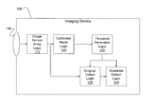
- FIG. 1 illustrates one example embodiment of an imaging device configured to correct output pixel values, associated with defective photo detectors of an image sensor array of the imaging device, on-the-fly in real-time;
- FIG. 2 illustrates an example embodiment of a graph representing a calibrated noise model implemented in the imaging device of FIG. 1 ;
- FIG. 3 illustrates one example embodiment of a method for correcting output pixel values in the imaging device of FIG. 1 ;
- FIG. 4A illustrates a first example embodiment of a 5 ⁇ 5 kernel of an image array of pixels in a Bayer pattern format
- FIG. 4B illustrates a second example embodiment of a 5 ⁇ 5 kernel of an image array of pixels in a Bayer pattern format
- FIG. 5 illustrates an example embodiment of a 5 ⁇ 5 kernel of an image array of pixels for illustrating the concept of singular defect detection
- FIG. 6 illustrates an example embodiment of a 5 ⁇ 5 kernel of an image array of pixels for illustrating the concept of clustered defect verification
- FIG. 7 illustrates an example embodiment of an image of an array of output pixels before correcting defects in the image
- FIG. 8 illustrates an example embodiment of an image of the array of output pixels of FIG. 7 after correcting defects in the image
- FIG. 9 illustrates one embodiment of a portion of the imaging device of FIG. 1 implemented as an integrated circuit device
- FIG. 10 illustrates one embodiment of another portion of the imaging device of FIG. 1 implemented as an integrated circuit device
- FIG. 11 illustrates one embodiment of the imaging device of FIG. 1 implemented with the integrated circuit devices of FIG. 9 and FIG. 10 .
- green color channels may refer to light green color channels, dark green color channels, or both.
- on-the-fly in real-time refers to occurring during imaging device run time as images are acquired by an imaging device (e.g., a camera).
- pixel means picture element and may refer to a data element generated from a photo detector of an image sensor array.
- pixel value as used herein, may refer to an output level of a photo detector of an image sensor array or to a value of a data element of an image array stored in a computer memory.
- the terms “pixel” and “pixel value” may be used interchangeably herein.
- color channel may refer to a hardware channel of an image sensor array logic corresponding to a color defined by a color filter of the image sensor array logic.
- color channel may refer to a data channel of an image array stored in a computer memory. In either case, a single color channel is associated with a single pixel.
- color channel type refers to a color of a color channel. When referring to multiple color channels herein, the multiple color channels may be of a same color channel type or of differing color channels types, for example.
- kernel defines a N ⁇ N (e.g., 5 ⁇ 5) square matrix region of pixels having a pixel-under-test at a center element of the matrix region.
- a defect correction process may be performed on the pixel-under-test by taking into consideration one or more pixel values within the kernel.
- a kernel may be moved or effectively aligned with respect to an image array of output pixels to consider different pixels as the pixel-under-test when performing a defect correction process on the image array of output pixels.
- the output from an image array contains red (R), light green (Gr), blue (B), and dark green (Gb) pixels arranged in an interleaving pattern.
- Such an interleaving pattern is often referred to as a Bayer pattern.
- the Gr pixels share the same rows with R pixels.
- the Gb pixels share the same rows with the B pixels. Therefore, there are four (4) color channel types for an image array output, namely Gr, R, B, Gb color channel types.
- one characteristic of a defective photo detector in an image sensor array is that its output value (output pixel value) is significantly different than the output values of its surrounding same color channel type photo detectors. Defects corresponding to a significantly larger value than the surrounding values are referred to as bright defects. Defects corresponding to a significantly smaller value than the surrounding values are referred to as dark defects.
- singular defect detection, verification, and correction are performed first, followed by clustered defect detection, verification, and correction.
- a singular pixel defect is defined as there being only one defective pixel (associated with a defective photo detector) within the same 5 ⁇ 5 kernel for a same color channel type.
- a clustered pixel defect is defined as there being more than one defective pixel (associated with more than one defective photo detector) within the same 5 ⁇ 5 kernel for a same color channel type. It is to be understood herein that pixels associated with a pixel array of output pixel values may be considered for singular defects and clustered defects and corrected, in accordance with various embodiments. That is, the output values associated with defective photo detectors may be corrected. The hardware of the actual defective photo detectors is not corrected or fixed.
- FIG. 1 illustrates one example embodiment of an imaging device 100 configured to correct output pixel values, associated with defective photo detectors of an image sensor array of the imaging device, on-the-fly in real-time.
- the imaging device 100 includes image sensor array logic 110 , calibrated noise logic 120 , singular defect logic 130 , clustered defect logic 140 , and threshold generation logic 150 .
- the imaging device 100 is implemented on a chip (i.e., a system-on-chip or SOC configuration) including one or more integrated circuits configured to perform one or more functions described herein.
- the imaging device 100 is implemented on several chips that are interconnected via, for example, traces on a printed circuit board (PCB).
- the imaging device 100 may be configured to also include discrete components such as, for example, resistors, capacitors, inductors, and transistors.
- at least some portions of the logics of the imaging device 100 may be part of an executable algorithm, configured to perform the functions of the logics, where the algorithm is stored in a non-transitory medium.
- the image sensor array logic 110 is operably positioned with respect to a lens 105 .
- the lens 105 is configured to capture and focus light toward the image sensor array logic 110 .
- the image sensor array logic 110 includes an array of photo detectors/sensors, for example, CMOS technology arranged into an array of photo detectors. Each photo detector is configured to convert impinging light (photons) from the lens 105 into electrical output signals (pixel values).
- the array of photo detectors produces and outputs an image array of pixels that may include millions of pixels (e.g., 8 megapixels).
- the image sensor array logic 110 also includes color filter array (CFA) technology providing a Bayer pattern of color channels including red (R), blue (B), light green (Gr), and dark green (Gb) color channel types.
- CFA color filter array
- the Bayer pattern of color channels is elaborated on later herein with respect to the remaining figures.
- the image sensor array logic 110 is operably connected to the calibrated noise logic 120 .
- the image sensor array logic 110 outputs an image array of output pixel values to the calibrated noise logic 120 .
- the calibrated noise logic 120 is configured to generate a noise estimate, ⁇ , for each pixel in the image array of output pixel values based on a calibrated noise model.
- FIG. 2 illustrates one example embodiment of a graph representing a calibrated noise model 200 implemented by the calibration noise logic 120 in the imaging device 100 of FIG. 1 .
- the noise estimate, ⁇ , for a given pixel is dependent on the pixel intensity or pixel output value.
- the calibrated noise model 200 is generated as part of a manufacturing process of the imaging device.
- the calibrated noise logic 120 is operably connected to the threshold generation logic 150 .
- the noise estimate, ⁇ , for each pixel of the image array of output pixel values is communicated to the threshold generation logic 150 .
- the threshold generation logic 150 is configured to generate threshold values for each pixel based on the noise estimates. For example, in one embodiment, a threshold value T i is generated by multiplying a corresponding noise estimate, ⁇ , by a tuning parameter, k i .
- the tuning parameters k i are generated as part of a manufacturing process of the imaging device, in accordance with one embodiment.
- each associated pixel may be evaluated as a pixel-under-test (PUT).
- PUT pixel-under-test
- Each PUT is evaluated by determining if the PUT is defective (or not defective) due to, for example, an associated defective photo detector.
- An associated pixel value of the PUT may be corrected upon verifying that the PUT is actually defective.
- singular pixel defects and clustered pixel defects are considered within a defined region (a kernel) around the PUT. In one embodiment, for a given PUT, singular pixel defects are considered first and clustered pixel defects are considered afterwards.
- the image sensor array logic 110 is also operably connected to the singular defect logic 130
- the threshold generation logic 150 is operably connected to the singular defect logic 130 .
- the singular defect logic 130 is configured to detect a potential defect in a pixel-under-test (PUT) upon inputting a portion (e.g., a 5 ⁇ 5 kernel) of the image array of output pixels. Also, the singular defect logic 130 is configured to verify that the PUT is actually defective. The singular defect logic 130 is further configured to correct the PUT when the PUT is identified as being actually defective. Details of the singular defect logic 130 functions of detecting, verifying, and correcting such singular defects, using threshold values provided by the threshold generation logic 150 , are elaborated on below herein with respect to the remaining figures.
- the singular defect logic 130 is operably connected to the clustered defect logic 140
- the threshold generation logic 150 is operably connected to the clustered defect logic 140 .
- the clustered defect logic 140 is configured to detect at least two potential defects within the portion (e.g., the 5 ⁇ 5 kernel) of the image array of output pixels based on the PUT of the image array of output pixels. Also, the clustered defect logic 140 is configured to verify that the PUT and one other pixel within the portion of the image array of output pixels are actually defective. The clustered defect logic 140 is further configured to correct the PUT when the PUT and one other pixel value within the portion of the image array of output pixels are identified as being actually defective. Details of the clustered defect logic 130 functions of detecting, verifying, and correcting such clustered defects, using threshold values provided by the threshold generation logic 150 , are elaborated on below herein with respect to the remaining figures.
- both singular defects and clustered defects may be detected, verified, and corrected.
- Algorithmic details for handling singular defects and clustered defects for an image array of output pixels are provided below herein.
- a pixel may be evaluated by a positive process to determine if that pixel is defective. If the pixel passes that positive process, the pixel is considered to be defective. If the pixel fails that positive process, the pixel is considered to not be defective (i.e., has been determined to not be defective). Similarly, in another embodiment, a pixel may be evaluated by a negative process to determine if that pixel is not defective. If the pixel passes that negative process, the pixel is considered to not be defective. If the pixel fails that negative process, the pixel is considered to be defective (i.e., has been determined to be defective).
- FIG. 3 illustrates one example embodiment of a method 300 for correcting output pixel values in the imaging device 100 of FIG. 1 .
- Method 300 is implemented to be performed by the imaging device 100 of FIG. 1 , or by a computing device (e.g., an integrated circuit device) configured with an algorithm of method 300 .
- Method 300 will be described from the perspective of a pixel-under-test (PUT) being at the center of a 5 ⁇ 5 kernel of an image array of output pixels formatted in a Bayer pattern of color channels. Also, method 300 will be described from the perspective of being performed by the imaging device 100 .
- PUT pixel-under-test
- FIG. 4A illustrates a first example embodiment of a 5 ⁇ 5 kernel of an image array of pixels in a Bayer pattern format.
- FIG. 4B illustrates a second example embodiment of a 5 ⁇ 5 kernel of an image array of pixels in a Bayer pattern format. The pixels of the 5 ⁇ 5 kernels are shown in four shades of gray, representing four different color channel types of the Bayer pattern.
- the four shades of gray are representative of blue (B) color channels, red (R) color channels, light green (Gr) color channels, and dark green (Gb) color channels.
- the Bayer pattern of the four color channel types results from a color filter array (CFA) aligned with an array of CMOS photo detectors in the image sensor array logic 110 .
- CFA color filter array
- each pixel in the 5 ⁇ 5 kernels is indexed by a pair of numbers indicating a matrix position in the 5 ⁇ 5 kernels.
- the center pixel (the pixel-under-test) is indexed by the pair of numbers 22 as shown in FIG. 4A and FIG. 4B .
- the pixel-under-test corresponds to a blue B color channel.
- the PUT corresponds to a dark green Gb color channel.
- the singular defect logic 130 determines a maximum pixel value (P max ) and a minimum pixel value (P min ) from eight pixels (P 1 -P 8 ) within the 5 ⁇ 5 kernel that surround the PUT and which correspond to a same color channel type as the PUT.
- P max max( P 1, P 2, . . . , P 8);
- P min min( P 1, P 2, . . . , P 8).
- FIG. 5 illustrates an example embodiment of a 5 ⁇ 5 kernel 500 of an image array of pixels for illustrating the concept of single defect detection.
- the PUT is labeled as Pc in FIG. 5
- eight (8) surrounding pixels within the 5 ⁇ 5 kernel that are of the same color channel type as the PUT are labeled as P 1 -P 8 .
- the locations of pixels P 1 -P 8 in the 5 ⁇ 5 kernel are determined by the Bayer pattern (e.g., see FIG. 4A and FIG. 4B ). However, for simplicity, the various shades of gray of the Bayer pattern on not shown in FIG. 5 .
- the singular defect logic 130 is configured to generate a first difference value by subtracting the maximum pixel value (P max ) from a value of the PUT, and a second difference value by subtracting the value of the PUT from the minimum pixel value (P min ).
- the singular defect logic 130 is further configured to identify the PUT as being potentially defective by determining that at least one of the first difference value and the second difference value is greater than a first threshold value T 1 generated by the threshold generation logic 150 .
- the PUT is identified as being potentially defective when: Pc ⁇ P max >T 1 (a bright defect) or P min ⁇ Pc>T 1 (a dark defect).
- the singular defect logic 130 is configured to verify that the PUT is actually defective (i.e., that the potential singular defect determined at 320 is not a false alarm).
- the singular defect logic 130 is configured to generate four (4) absolute difference values by subtracting the value of the PUT from a pixel value of each of four (4) different nearest dark green Gb (or light green Gr) pixel color channels immediately surrounding the PUT within the 5 ⁇ 5 kernel, and taking the absolute value. For example, referring to FIG. 4B , the dark green PUT at matrix location 22 is surrounded by four (4) nearest light green pixels at matrix locations 11 , 13 , 31 , and 33 .
- the singular defect logic 130 is further configured to identify the PUT as being actually defective by determining that at least three (3) of the four (4) absolute difference values are greater than a second threshold value T 2 generated by the threshold generation logic. That is, the light green (or dark green) PUT is identified as being actually defective when
- the singular defect logic 130 is configured to correct the PUT (i.e., the value of the pixel-under-test).
- the value of the PUT is corrected by replacing the value of the PUT with the value of P max when the defect is a bright defect (i.e., when Pc—P max >T 1 ).
- the value of the PUT is corrected by replacing the value of the PUT with the value of P min when the defect is a dark defect (i.e., when P min ⁇ Pc>T 1 ). In this manner, the output values of singularly defective pixels corresponding to light green Gr or dark green Gb color channels may be corrected.
- the singular defect logic 130 is configured to verify that the PUT is actually defective (i.e., that the potential singular defect determined at 320 is not a false alarm).
- the singular defect logic 130 is configured to generate a first average value (Avg 1 ) from pixel values of four (4) nearest pixels surrounding the PUT, within the 5 ⁇ 5 kernel, which correspond to four (4) nearest green (light green, dark green, or both) color channels.
- Avg 1 a first average value from pixel values of four (4) nearest pixels surrounding the PUT, within the 5 ⁇ 5 kernel, which correspond to four (4) nearest green (light green, dark green, or both) color channels.
- the four (4) nearest green color channels are located at matrix locations 12 , 21 , 23 , and 32 .
- the singular defect logic 130 is configured to generate a second average value (Avg 2 ) from pixel values of eight (8) farthest pixels surrounding the PUT, within the 5 ⁇ 5 kernel, which correspond to eight (8) farthest green (light green, dark green, or both) color channels.
- the eight (8) farthest green color channels are located at matrix locations 01 , 03 , 10 , 14 , 30 , 34 , 41 , and 43 .
- the singular defect logic 130 is further configured to generate a bright defect difference value by subtracting the second average value (Avg 2 ) from the first average value (Avg 1 ).
- the singular defect logic 130 is also configured to generate a dark defect difference value by subtracting the first average value (Avg 1 ) from the second average value (Avg2).
- the singular defect logic 130 is configured to identify the PUT as being actually defective by determining that at least one of the bright defect difference value or that the dark defect difference value is less than a third threshold value T 3 .
- the red R or blue B PUT is identified as being actually defective when: Avg 1 ⁇ Avg 2 ⁇ T 3 or Avg 2 ⁇ Avg 1 ⁇ T 3 .
- the singular defect logic 130 is configured to correct the PUT (i.e., the value of the pixel-under-test).
- the value of the PUT is replaced by the value of P max when the defect is a bright defect (i.e., when Pc ⁇ P max >T 1 ).
- the value of the PUT is replaced by the value of P min when the defect is a dark defect (i.e., when P min ⁇ Pc>T 1 ). In this manner, the output values of singularly defective pixels corresponding to red R or blue B color channels may be corrected.
- a potential singular defect has not been detected at 320 , has not been verified at 330 , or has been corrected at 340 , then the method 300 proceeds to 350 .
- a determination is made as to whether at least two pixels in the 5 ⁇ 5 kernel are potentially defective (i.e., a clustered defect is potentially present). The determination is made by the clustered defect logic 140 of FIG. 1 using information from the singular defect logic 130 .
- the clustered defect logic 140 is configured to determine a second largest pixel value (Pmax 2 ) and a second smallest pixel value (Pmin 2 ) from the eight (8) pixels within the 5 ⁇ 5 kernel that surround the PUT and which correspond to a same color channel type as the PUT.
- P max 2 max( P 1, P 2, . . . , P 8), excluding P max
- P min 2 min( P 1, P 2, . . . , P 8),excluding P min .
- the clustered defect logic 140 is also configured to generate a third difference value by subtracting the second largest pixel value from the value of the PUT.
- the clustered defect logic 140 is further configured to generate a fourth difference value by subtracting the second largest pixel value from the maximum pixel value.
- the clustered defect logic 140 is also configured to generate a fifth difference value by subtracting the value of the PUT from the second smallest pixel value Pmin 2 .
- the clustered defect logic 140 is further configured to generate a sixth difference value by subtracting the minimum pixel value P min from the second smallest pixel value Pmin 2 .
- the clustered defect logic 140 is configured to identify the PUT and a first pixel corresponding to the maximum pixel value P max as being potentially defective by determining when the third difference value and the fourth difference value are each greater than a fourth threshold value T 4 .
- the clustered defect logic 140 is configured to identify the PUT and a second pixel corresponding to the minimum pixel value P min as being potentially defective by determining when the fifth difference value and the sixth difference value are each greater than the fourth threshold value T 4 .
- the clustered defect logic 140 is configured to verify that the PUT and one of the first pixel (corresponding to P max ) and the second pixel (corresponding to P min ) are actually defective.
- FIG. 6 illustrates an example embodiment of a 5 ⁇ 5 kernel 600 of an image array of pixels for illustrating the concept of clustered defect verification.
- an intermediate pixel Pk is considered.
- the intermediate pixel Pk corresponds to a different color channel type than that of the PUT and the first and second pixels, and is located between the PUT (Pc) and one of the first pixel and the second pixel (e.g., P 1 in FIG. 6 ) within the 5 ⁇ 5 kernel. Notice that Pc, Pk, and P 1 appear in a straight line in FIG. 6 . If the intermediate pixel Pk has previously been determined to not be defective by the singular defect logic 130 , then the PUT (Pc) and the first or second pixel (e.g., P 1 in FIG. 6 ) are verified as being actually defective. Again, it is noted herein that embodiments being configured to determine that a pixel is defective (potentially or actually) are also inherently configured to determine that the pixel is not defective, and vice versa.
- the clustered defect logic 140 is configured to correct the PUT (i.e., the value of the pixel-under-test).
- the PUT is corrected by replacing the value of the PUT with the second largest pixel value Pmax 2 , when the clustered defect is considered to be a bright clustered defect (i.e., when Pc ⁇ Pmax 2 >T 4 and P max ⁇ Pmax 2 >T a ).
- the PUT is corrected by replacing the value of the PUT with the second smallest pixel value Pmin 2 , when the clustered defect is considered to be a dark clustered defect (i.e., when Pmin 2 ⁇ Pc>T 4 and Pmin 2 ⁇ P min >T 4 ).
- the output value of a defective pixel associated with a cluster of defective pixels may be corrected.
- the PUT is corrected by replacing the value of the PUT with the second smallest pixel value Pmin 2 , when the clustered defect is considered to be a dark clustered defect (i.e., when Pmin 2 , Pc>T 4 and Pmin 2 ⁇ P min >T 4 ).
- a potential clustered defect has not been detected at 350 , has not been verified at 360 , or has been corrected at 370 , then the method 300 proceeds to 380 .
- a determination is made as to whether the end of the image has been reached in the method 300 . That is, a determination is made as to whether all of the pixels in the image array of output pixels have been considered as a pixel-under-test (PUT). If all of the pixels have not been considered, then method 300 reverts back to 310 , where a new PUT centered within a new 5 ⁇ 5 kernel of the image array is considered. Otherwise, method 300 ends.
- all pixels associated with a pixel array of output pixels values may be considered for singular defects and clustered defects and may be corrected on-the-fly in real-time, in accordance with various embodiments. That is, the output values associated with, for example, defective photo detectors may be corrected. The actual defective photo detectors and/or defective associated hardware are not corrected or fixed.
- FIG. 7 illustrates an example embodiment of an image 700 of an array of output pixels before correcting defects in the image.
- the image includes uncorrupted pixels having no defects (including certain bright spatial features) as well as a corrupted pixel corresponding to a singular defect and corrupted pixels corresponding to a clustered defect.
- FIG. 8 illustrates an example embodiment of an image 800 of the array of output pixels of FIG. 7 after correcting defects in the image. As shown in FIG. 8 , both the singular defect and the clustered defect have been corrected in accordance with method 300 of FIG. 3 as implemented in the imaging device 100 of FIG. 1 .
- an imaging device includes image sensor array logic, calibrated noise logic, threshold generation logic, singular defect logic, and clustered defect logic.
- the image sensor array logic is configured to generate an image array of output pixels in a Bayer pattern.
- the calibrated noise logic is configured to generate a noise estimate for each pixel.
- the singular defect logic is configured to identify a pixel-under-test (from a 5 ⁇ 5 kernel of the image array of output pixels) as being potentially defective (e.g., due to a defective associated photo detector of the sensor array logic), verify that the pixel-under-test is actually defective, and correct the pixel-under-test.
- the singular defect logic implements a first algorithm to perform detection, verification, and correction.
- the first algorithm uses thresholds generated by the threshold generation logic. Generation of the thresholds is based on noise estimates from the calibrated noise logic.
- the clustered defect logic is configured to identify a pixel-under-test and another pixel (from the 5 ⁇ 5 kernel of the image array of output pixels) as being potentially defective (e.g., due to defective associated photo detectors of the sensor array logic), verify that the pixel-under-test and the other pixel are actually defective, and correct the pixel-under-test.
- the clustered defect logic implements a second algorithm to perform detection, verification, and correction.
- the second algorithm uses thresholds generated by the threshold generation logic. Generation of the thresholds is based on noise estimates from the calibrated noise logic.
- the imaging device 100 may be on one or more integrated circuit chips (e.g., image signal processing chips).
- FIG. 9 illustrates one embodiment of a portion of the imaging device 100 of FIG. 1 implemented as an integrated circuit device 900 for correcting defective pixel outputs on-the-fly in real-time.
- the singular defect logic 130 is embodied as a separate integrated circuit 910 .
- the clustered defect logic 140 is embodied on an individual integrated circuit 920 .
- the threshold generation logic 150 is also embodied on an individual integrated circuit 930 .
- circuits 910 , 920 , and 930 are connected via connection paths to communicate signals. While integrated circuits 910 , 920 , and 930 are illustrated as separate integrated circuits, they may be integrated into a common integrated circuit device 900 . Additionally, integrated circuits 910 , 920 , and 930 may be combined into fewer integrated circuits or divided into more integrated circuits than illustrated.
- the singular defect logic 130 , the clustered defect logic 140 , and the threshold generation logic 150 may be combined into a separate application-specific integrated circuit.
- portions of the functionality associated with the singular defect logic 130 , the clustered defect logic 140 , and the threshold generation logic 150 may be embodied as firmware executable by a processor and stored in a non-transitory memory (e.g., a non-transitory computer storage medium).
- FIG. 10 illustrates one embodiment of another portion of the imaging device 100 of FIG. 1 implemented as an integrated circuit device 1000 for correcting defective pixels outputs on-the-fly in real-time.
- the image sensor array logic 110 is embodied as a separate integrated circuit 1010 .
- the calibrated noise logic 120 is embodied on an individual integrated circuit 1020 .
- circuits 1010 and 1020 are connected via connection paths to communicate signals. While integrated circuits 1010 and 1020 are illustrated as separate integrated circuits, they may be integrated into a common integrated circuit device 1000 . Additionally, integrated circuits 1010 and 1020 may be combined into fewer integrated circuits or divided into more integrated circuits than illustrated.
- the image sensor array logic 110 and the calibrated noise logic 120 may be combined into a separate application-specific integrated circuit.
- portions of the functionality associated with the image sensor array logic 110 and the calibrated noise logic 120 may be embodied as firmware executable by a processor and stored in a non-transitory memory (e.g., a non-transitory computer storage medium).
- the integrated circuit device 900 and the integrated circuit device 1000 are implemented in a single imaging device 100 , as shown in FIG. 11 , and are connected via connection paths to communicate signals.
- the integrated circuits 910 , 920 , 930 , 1010 , and 1020 may be combined into a single integrated circuit device and are connected via connection paths to communicate signals.
- references to “one embodiment”, “an embodiment”, “one example”, “an example”, and so on, indicate that the embodiment(s) or example(s) so described may include a particular feature, structure, characteristic, property, element, or limitation, but that not every embodiment or example necessarily includes that particular feature, structure, characteristic, property, element or limitation. Furthermore, repeated use of the phrase “in one embodiment” does not necessarily refer to the same embodiment, though it may.
- Computer-readable medium or “computer storage medium”, as used herein, refers to a non-transitory medium that stores instructions and/or data configured to perform one or more of the disclosed functions when executed.
- a computer-readable medium may take forms, including, but not limited to, non-volatile media, and volatile media.
- Non-volatile media may include, for example, optical disks, magnetic disks, and so on.
- Volatile media may include, for example, semiconductor memories, dynamic memory, and so on.
- a computer-readable medium may include, but are not limited to, a floppy disk, a flexible disk, a hard disk, a magnetic tape, other magnetic medium, an application specific integrated circuit (ASIC), a programmable logic device, a compact disk (CD), other optical medium, a random access memory (RAM), a read only memory (ROM), a memory chip or card, a memory stick, solid state storage device (SSD), flash drive, and other media from which a computer, a processor or other electronic device can function with.
- ASIC application specific integrated circuit
- CD compact disk
- RAM random access memory
- ROM read only memory
- memory chip or card a memory chip or card
- SSD solid state storage device
- flash drive and other media from which a computer, a processor or other electronic device can function with.
- Each type of media if selected for implementation in one embodiment, may include stored instructions of an algorithm configured to perform one or more of the disclosed and/or claimed functions.
- Computer-readable media described herein are limited to statutory subject matter under 35 U.
- Logic represents a component that is implemented with computer or electrical hardware, firmware, a non-transitory medium with stored instructions of an executable application or program module, and/or combinations of these to perform any of the functions or actions as disclosed herein, and/or to cause a function or action from another logic, method, and/or system to be performed as disclosed herein.
- Logic may include a microprocessor programmed with an algorithm, a discrete logic (e.g., ASIC), at least one circuit, an analog circuit, a digital circuit, a programmed logic device, a memory device containing instructions of an algorithm, and so on, any of which are configured to perform one or more of the disclosed functions.
- logic may include one or more gates, combinations of gates, or other circuit components configured to perform one or more of the disclosed functions. Where multiple logics are described, it may be possible to incorporate the multiple logics into one logic. Similarly, where a single logic is described, it may be possible to distribute that single logic between multiple logics. In one embodiment, one or more of these logics are corresponding structure associated with performing the disclosed and/or claimed functions. Choice of which type of logic to implement may be based on desired system conditions or specifications. Logic is limited to statutory subject matter under 35 U.S.C. ⁇ 101.
- An “operable connection”, or a connection by which entities are “operably connected”, is one in which signals, physical communications, and/or logical communications may be sent and/or received.
- An operable connection may include a physical interface, an electrical interface, and/or a data interface.
- An operable connection may include differing combinations of interfaces and/or connections sufficient to allow operable control.
- two entities can be operably connected to communicate signals to each other directly or through one or more intermediate entities (e.g., processor, operating system, logic, non-transitory computer-readable medium).
- Logical and/or physical communication channels can be used to create an operable connection.
- illustrated methodologies are shown and described as a series of blocks. The methodologies are not limited by the order of the blocks as some blocks can occur in different orders and/or concurrently with other blocks from that shown and described. Moreover, less than all the illustrated blocks may be used to implement an example methodology. Blocks may be combined or separated into multiple components. Furthermore, additional and/or alternative methodologies can employ additional actions that are not illustrated in blocks. The methods described herein are limited to statutory subject matter under 35 U.S.C ⁇ 101.
- the phrase “one or more of, A, B, and C” is used herein, (e.g., a data store configured to store one or more of, A, B, and C) it is intended to convey the set of possibilities A, B, C, AB, AC, BC, and/or ABC (e.g., the data store may store only A, only B, only C, A&B, A&C, B&C, and/or A&B&C). It is not intended to require one of A, one of B, and one of C.
- the applicants intend to indicate “at least one of A, at least one of B, and at least one of C”, then the phrasing “at least one of A, at least one of B, and at least one of C” will be used.
Abstract
Description
P max=max(P1,P2, . . . ,P8);
P min=min(P1,P2, . . . ,P8).
Pc−P max >T 1 (a bright defect) or P min −Pc>T 1 (a dark defect).
Avg1−Avg2 <T 3 or Avg2−Avg1 <T 3.
Pmax2=max(P1,P2, . . . ,P8), excluding P max;
Pmin2=min(P1,P2, . . . ,P8),excluding P min.
Third difference value=Pc−Pmax2;
Fourth difference value=P max −PMax2;
Fifth difference value=Pmin2 −Pc;
Sixth difference value=Pmin2 −P min.
Pc−Pmax2 >T 4 and P max −Pmax2 >T 4.
Pmin2 −Pc>T 4 and Pmin2 −P min >T 4.
Claims (19)
Priority Applications (1)
| Application Number | Priority Date | Filing Date | Title |
|---|---|---|---|
| US14/569,868 US9578320B1 (en) | 2014-01-03 | 2014-12-15 | Methods and apparatus for defect correction in image sensor outputs |
Applications Claiming Priority (2)
| Application Number | Priority Date | Filing Date | Title |
|---|---|---|---|
| US201461923345P | 2014-01-03 | 2014-01-03 | |
| US14/569,868 US9578320B1 (en) | 2014-01-03 | 2014-12-15 | Methods and apparatus for defect correction in image sensor outputs |
Publications (1)
| Publication Number | Publication Date |
|---|---|
| US9578320B1 true US9578320B1 (en) | 2017-02-21 |
Family
ID=58017777
Family Applications (1)
| Application Number | Title | Priority Date | Filing Date |
|---|---|---|---|
| US14/569,868 Expired - Fee Related US9578320B1 (en) | 2014-01-03 | 2014-12-15 | Methods and apparatus for defect correction in image sensor outputs |
Country Status (1)
| Country | Link |
|---|---|
| US (1) | US9578320B1 (en) |
Cited By (3)
| Publication number | Priority date | Publication date | Assignee | Title |
|---|---|---|---|---|
| US10547800B2 (en) | 2017-05-24 | 2020-01-28 | Samsung Electronics Co., Ltd. | Pixel circuit and image sensor including thereof |
| US20220180498A1 (en) * | 2020-12-09 | 2022-06-09 | SK Hynix Inc. | Image sensing device |
| CN114913176A (en) * | 2022-07-18 | 2022-08-16 | 江苏启航箱包有限公司 | Flexible leather material scab defect detection method and system based on artificial intelligence |
Citations (7)
| Publication number | Priority date | Publication date | Assignee | Title |
|---|---|---|---|---|
| US20090129695A1 (en) * | 2007-11-15 | 2009-05-21 | Aldrich Bradley C | Method and system for noise management for spatial processing in digital image/video capture systems |
| US20130162871A1 (en) * | 2011-12-23 | 2013-06-27 | Stmicroelectronics S.R.L. | Color filter array defect correction |
| US20130229531A1 (en) * | 2012-03-05 | 2013-09-05 | Apple Inc. | Camera blemish defects detection |
| US20130321674A1 (en) * | 2012-05-31 | 2013-12-05 | Apple Inc. | Image Signal Processing Involving Geometric Distortion Correction |
| US20130321679A1 (en) * | 2012-05-31 | 2013-12-05 | Apple Inc. | Systems and methods for highlight recovery in an image signal processor |
| US20130321675A1 (en) * | 2012-05-31 | 2013-12-05 | Apple Inc. | Raw scaler with chromatic aberration correction |
| US20150296193A1 (en) * | 2012-05-31 | 2015-10-15 | Apple Inc. | Systems and methods for rgb image processing |
-
2014
- 2014-12-15 US US14/569,868 patent/US9578320B1/en not_active Expired - Fee Related
Patent Citations (7)
| Publication number | Priority date | Publication date | Assignee | Title |
|---|---|---|---|---|
| US20090129695A1 (en) * | 2007-11-15 | 2009-05-21 | Aldrich Bradley C | Method and system for noise management for spatial processing in digital image/video capture systems |
| US20130162871A1 (en) * | 2011-12-23 | 2013-06-27 | Stmicroelectronics S.R.L. | Color filter array defect correction |
| US20130229531A1 (en) * | 2012-03-05 | 2013-09-05 | Apple Inc. | Camera blemish defects detection |
| US20130321674A1 (en) * | 2012-05-31 | 2013-12-05 | Apple Inc. | Image Signal Processing Involving Geometric Distortion Correction |
| US20130321679A1 (en) * | 2012-05-31 | 2013-12-05 | Apple Inc. | Systems and methods for highlight recovery in an image signal processor |
| US20130321675A1 (en) * | 2012-05-31 | 2013-12-05 | Apple Inc. | Raw scaler with chromatic aberration correction |
| US20150296193A1 (en) * | 2012-05-31 | 2015-10-15 | Apple Inc. | Systems and methods for rgb image processing |
Cited By (7)
| Publication number | Priority date | Publication date | Assignee | Title |
|---|---|---|---|---|
| US10547800B2 (en) | 2017-05-24 | 2020-01-28 | Samsung Electronics Co., Ltd. | Pixel circuit and image sensor including thereof |
| US10897587B2 (en) | 2017-05-24 | 2021-01-19 | Samsung Electronics Co., Ltd. | Pixel circuit and image sensor including thereof |
| US11184566B2 (en) | 2017-05-24 | 2021-11-23 | Samsung Electronics Co., Ltd. | Pixel circuit and image sensor including thereof |
| US11778344B2 (en) | 2017-05-24 | 2023-10-03 | Samsung Electronics Co., Ltd. | Pixel circuit and image sensor including thereof |
| US20220180498A1 (en) * | 2020-12-09 | 2022-06-09 | SK Hynix Inc. | Image sensing device |
| CN114615448A (en) * | 2020-12-09 | 2022-06-10 | 爱思开海力士有限公司 | Image sensing device |
| CN114913176A (en) * | 2022-07-18 | 2022-08-16 | 江苏启航箱包有限公司 | Flexible leather material scab defect detection method and system based on artificial intelligence |
Similar Documents
| Publication | Publication Date | Title |
|---|---|---|
| US11470245B2 (en) | System and method for fault detection and correction | |
| US8189050B1 (en) | Filtering systems and methods for infrared image processing | |
| CN103026720B (en) | The optics self diagnosis of stereo camera system | |
| EP1781017B1 (en) | Methods and devices for image signal processing | |
| CN101277385B (en) | Method and apparatus to detect a dead pixel of an image sensor and method and apparatus to capture an image from an image sensor | |
| US8582005B2 (en) | Method, apparatus and system providing adjustment of pixel defect map | |
| US20160105656A1 (en) | White balance method in multi-exposure imaging system | |
| US11645743B2 (en) | Method, medium, and system for detecting potato virus in a crop image | |
| US9578320B1 (en) | Methods and apparatus for defect correction in image sensor outputs | |
| US9900533B2 (en) | Image processing apparatus and method, and image capturing apparatus | |
| US9521339B2 (en) | Image processing apparatus, image capturing apparatus, and image processing method | |
| US8310570B1 (en) | Repairing defective pixels | |
| KR20200106854A (en) | Pixel correction | |
| US6987577B2 (en) | Providing a partial column defect map for a full frame image sensor | |
| US9628659B2 (en) | Method and apparatus for inspecting an object employing machine vision | |
| CN104980718A (en) | Color correction devices and methods | |
| US8345965B2 (en) | Method and apparatus for positioning edges of photograph | |
| US9122935B2 (en) | Object detection method, storage medium, integrated circuit, and object detection apparatus | |
| US11428634B2 (en) | Method for localizing signal sources in localization microscopy | |
| WO2018198916A1 (en) | Image processing device, image processing method and storage medium | |
| US8417019B2 (en) | Image correction system and method | |
| WO2017221376A1 (en) | Image processing device, image processing method, and image processing program | |
| KR20100037339A (en) | Apparatus and method for correcting defect pixels | |
| US20230032323A1 (en) | Image processing method and system | |
| CN114095721B (en) | Method and device for detecting video dead pixel and computer readable medium |
Legal Events
| Date | Code | Title | Description |
|---|---|---|---|
| AS | Assignment |
Owner name: MARVELL INTERNATIONAL LTD., BERMUDA Free format text: ASSIGNMENT OF ASSIGNORS INTEREST;ASSIGNOR:MARVELL SEMICONDUCTOR, INC.;REEL/FRAME:041154/0118 Effective date: 20161216 Owner name: MARVELL SEMICONDUCTOR, INC., CALIFORNIA Free format text: ASSIGNMENT OF ASSIGNORS INTEREST;ASSIGNOR:LI, HUAI DONG;REEL/FRAME:041154/0050 Effective date: 20141230 |
|
| STCF | Information on status: patent grant |
Free format text: PATENTED CASE |
|
| AS | Assignment |
Owner name: CAVIUM INTERNATIONAL, CAYMAN ISLANDS Free format text: ASSIGNMENT OF ASSIGNORS INTEREST;ASSIGNOR:MARVELL INTERNATIONAL LTD.;REEL/FRAME:052918/0001 Effective date: 20191231 |
|
| AS | Assignment |
Owner name: MARVELL ASIA PTE, LTD., SINGAPORE Free format text: ASSIGNMENT OF ASSIGNORS INTEREST;ASSIGNOR:CAVIUM INTERNATIONAL;REEL/FRAME:053475/0001 Effective date: 20191231 |
|
| FEPP | Fee payment procedure |
Free format text: MAINTENANCE FEE REMINDER MAILED (ORIGINAL EVENT CODE: REM.); ENTITY STATUS OF PATENT OWNER: LARGE ENTITY |
|
| LAPS | Lapse for failure to pay maintenance fees |
Free format text: PATENT EXPIRED FOR FAILURE TO PAY MAINTENANCE FEES (ORIGINAL EVENT CODE: EXP.); ENTITY STATUS OF PATENT OWNER: LARGE ENTITY |
|
| STCH | Information on status: patent discontinuation |
Free format text: PATENT EXPIRED DUE TO NONPAYMENT OF MAINTENANCE FEES UNDER 37 CFR 1.362 |
|
| FP | Lapsed due to failure to pay maintenance fee |
Effective date: 20210221 |