US9577653B2 - Quasi-linear spin torque nano-oscillators - Google Patents
Quasi-linear spin torque nano-oscillators Download PDFInfo
- Publication number
- US9577653B2 US9577653B2 US14/760,999 US201414760999A US9577653B2 US 9577653 B2 US9577653 B2 US 9577653B2 US 201414760999 A US201414760999 A US 201414760999A US 9577653 B2 US9577653 B2 US 9577653B2
- Authority
- US
- United States
- Prior art keywords
- magnetic
- spin
- bias
- torque
- layer
- Prior art date
- Legal status (The legal status is an assumption and is not a legal conclusion. Google has not performed a legal analysis and makes no representation as to the accuracy of the status listed.)
- Active
Links
Images


Classifications
-
- H—ELECTRICITY
- H03—ELECTRONIC CIRCUITRY
- H03L—AUTOMATIC CONTROL, STARTING, SYNCHRONISATION, OR STABILISATION OF GENERATORS OF ELECTRONIC OSCILLATIONS OR PULSES
- H03L7/00—Automatic control of frequency or phase; Synchronisation
- H03L7/26—Automatic control of frequency or phase; Synchronisation using energy levels of molecules, atoms, or subatomic particles as a frequency reference
-
- H—ELECTRICITY
- H03—ELECTRONIC CIRCUITRY
- H03B—GENERATION OF OSCILLATIONS, DIRECTLY OR BY FREQUENCY-CHANGING, BY CIRCUITS EMPLOYING ACTIVE ELEMENTS WHICH OPERATE IN A NON-SWITCHING MANNER; GENERATION OF NOISE BY SUCH CIRCUITS
- H03B15/00—Generation of oscillations using galvano-magnetic devices, e.g. Hall-effect devices, or using superconductivity effects
- H03B15/006—Generation of oscillations using galvano-magnetic devices, e.g. Hall-effect devices, or using superconductivity effects using spin transfer effects or giant magnetoresistance
Definitions
- This patent document relates to systems, devices, and processes that use spin torque magnetic structures.
- Electrons and other charged particles process spins as one of their intrinsic particle properties and such a spin is associated with a spin angular momentum.
- a spin of an electron has two distinctive spin states. Electrons in an electrical current may be unpolarized by having the equal probabilities in the two spin states. The electrons in an electrical current are spin polarized by having more electrons in one spin state than electrons in the other spin state.
- a spin-polarized current can be achieved by manipulating the spin population via various methods, e.g., by passing the current through a magnetic layer having a particular magnetization.
- a spin-polarized current can be directed into a magnetic layer to cause transfer of the angular momenta of the spin-polarized electrons to the magnetic layer and this transfer can lead to exertion of a spin-transfer torque on the local magnetic moments in the magnetic layer and precession of the magnetic moments in the magnetic layer. Under a proper condition, this spin-transfer torque can cause a flip or switch of the direction of the magnetization of the magnetic layer.
- STNOs spin-torque nano-oscillators
- STNOs spin-torque nano-oscillators
- STNOs spin polarized currents to excite nano magnets that undergo persistent oscillations at RF or microwave frequencies.
- the spin currents are applied in a non-uniform manner to both excite the nano magnets into oscillations and generate dynamic damping at large amplitude as a feedback to reduce the nonlinearity associated with mixing amplitude and phase fluctuations.
- a method for generating an RF or microwave oscillation signal includes configuring a magnetic spin-torque structure to include a multi-layer stack of layers on a substrate to exhibit a spin-torque effect, wherein the multi-layer stack is shaped to have a shape anisotropy in each layer and includes a thin magnetic free layer and a thick magnetic reference layer; applying a DC bias current to flow through the magnetic spin-torque structure; applying a bias magnetic field to the magnetic spin-torque structure; and controlling the DC bias current and the bias magnetic field to control a magnetic precession in the magnetic spin-torque structure to convert the DC bias current into an RF or microwave oscillation signal and effectuate a negative spin torque feedback to render a coupling between amplitude and phase fluctuations of the RF or microwave oscillation signal to be very weak or nearly zero, resulting in a nearly linear oscillator whose frequency varies at most only weakly with oscillator amplitude (power) at the optimum operating condition.
- the multi-layer stack is shaped to
- a spin-torque oscillator device for generating an RF or microwave oscillation signal to include a substrate; a magnetic spin-torque structure formed on the substrate and structured to include a multi-layer stack of layers on the substrate to exhibit a spin-torque effect, wherein the multi-layer stack is shaped to have a shape anisotropy in each layer and includes a thin magnetic free layer and a thick magnetic reference layer; a circuit coupled to the magnetic spin-torque structure to apply a DC bias current to flow through the magnetic spin-torque structure; and a magnetic field module configured to apply a bias magnetic field to the magnetic spin-torque structure.
- the magnetic spin-torque structure, the DC bias current and the bias magnetic field are configured to control a magnetic precession in the magnetic spin-torque structure to convert the DC bias current into an RF or microwave oscillation signal and effectuate a negative spin torque feedback to render a coupling between amplitude and phase fluctuations of the RF or microwave oscillation signal to be nearly zero.
- a method for generating a tunable RF or microwave oscillation signal from a magnetic spin-torque structure.
- This structure includes a multi-layer stack of layers including a magnetic free layer and a magnetic reference layer spaced from each other and shaped to have a shape anisotropy to exhibit a spin-torque effect and a magnetic precession in the magnetic spin-torque structure under a bias magnetic field.
- the method includes applying a DC bias current to flow through the magnetic spin-torque structure; applying a bias magnetic field to the magnetic spin-torque structure to include a bias magnetic field component that is in a plane of the magnetic free layer and perpendicular to an elongated direction of the magnetic free layer; and controlling the DC bias current and the bias magnetic field to control a magnetic precession in the magnetic spin-torque structure to convert the DC bias current into an RF or microwave oscillation signal and to reduce a coupling between an amplitude and an oscillation frequency of the RF or microwave oscillation signal.
- a spin-torque oscillator device for generating an RF or microwave oscillation signal to include a substrate and a magnetic spin-torque structure formed on the substrate and structured to include a multi-layer stack of layers on the substrate to exhibit a spin-torque effect.
- the multi-layer stack is shaped to have a shape anisotropy in each layer and includes a magnetic free layer, a magnetic reference layer and a conductive spacer layer between the magnetic free layer and the magnetic reference layer, and the magnetic reference layer has a tapered shape along a direction perpendicular to the magnetic reference layer.
- This device also includes a circuit coupled to the magnetic spin-torque structure to apply a DC bias current to flow through the magnetic spin-torque structure; and a magnetic field module configured to apply a bias magnetic field to the magnetic spin-torque structure.
- the magnetic spin-torque structure, the DC bias current and the bias magnetic field are configured to control a magnetic precession in the magnetic spin-torque structure to convert the DC bias current into an RF or microwave oscillation signal which has an oscillation frequency that is stabilized with respect to a power of the RF or microwave signal.
- FIG. 1A shows an example of a STNO device based on the disclosed STNO technology.
- FIG. 1B shows an example of an implementation of a STNO device in FIG. 1A .
- FIG. 1C illustrates an example of a multi-layer structure of a spin torque nano-oscillator as one implementation of the STNO device design in FIG. 1A .
- FIG. 2 includes FIGS. 2 a , 2 b , 2 c and 2 d showing sample measurements in a sample STNO device under an in-plane magnetic bias field H y .
- (c) oscillator power p n ( P/I dc 2 ) and normalized power p; and
- ⁇ f meas as the function of I dc , all for H y 700 Oe, 820 Oe and 880 Oe.
- FIG. 3 includes FIGS. 3 a , 3 b , 3 c and 3 d showing sample measurements in the same sample STNO device in FIG. 2 .
- FIG. 4 includes FIGS. 4 a , 4 b , 4 c and 4 d showing sample measurements in the same sample STNO device in FIG. 2 .
- ⁇ RL out-of-plane orientation
- ⁇ J c Variation of 1/cos ( ⁇ ) ( ⁇ J c ) along the easy axis of the FL where ⁇ is the in-plane offset angle between the FL and RL magnetization as determined by micromagnetics calculations.
- FIGS. 5, 6, 7 and 8 show various simulations of our sample STNO device.
- FIG. 9 includes FIGS. 9 a and 9 b .
- FIG. 11 includes FIGS. 11 a , 11 b , 11 c and 11 d .
- I c for the onset of the auto-oscillation and the value of the initial offset angle ⁇ o determined from I c , both as a function of H y .
- (b) Measured ⁇ f meas ⁇ p 0 .
- (d) Measured oscillator linewidth ⁇ f meas for I ⁇ 4 mA. Also shown is the predicted linewidth ⁇ f pred using the values of p o shown in (c) and the measured values of I df/dI.
- FIG. 12 includes FIGS. 12 a , 12 b , 12 c and 12 d .
- (a) Effective damping vs. I for H y 700 Oe. Up to I c ( ⁇ 2.6 mA) ⁇ eff /2 ⁇ drops rapidly with increasing I due to the anti-damping ST effect on the thermally generated oscillation. Above ⁇ 3.25 mA, ⁇ eff /2 ⁇ increases approximately linearly as the variation of oscillation power with bias becomes weaker and weaker.
- FIG. 13 includes FIGS. 13 a , 13 b and 13 c :
- (a) Normalized oscillator power p o,mms vs. I, as determined from the MMS for H y 800 Oe. Also shown is the mean offset angle ⁇ 0 averaged over the simulated FL.
- (b) The out-of-plane orientation ( ⁇ RL ) of the RL magnetization as the function of position along its elongated (easy) axis, as determined by MMS for H y 800 Oe.
- the estimated H Oe ⁇ 26 Oe/mA is partially cancelled by H st ip ⁇ 15 Oe/mA in the end regions of the FL.
- the modeled value of ⁇ RL ⁇ 12° is determined by averaging the result of the static micromagnetic simulation over several unit cells at the end of the RL
- the ST applied to the center area drives the oscillations while the ST at the edges provides enhanced dynamic damping when the local orientation between the FL and RL magnetization is near 90°.
- STT spin-transfer torque
- MRAM magnetic random access memory
- FL free layer or free magnetic layer
- RL reference layer
- PL fixed magnetization
- a STT-MRAM circuit can include a magnetic tunnel junction (MTJ) as a magnetoresistive element formed of two or more thin film ferromagnetic layers including a free layer (FL) and a reference layer (RL) that are separated by an insulating barrier layer (e.g., a MgO layer) that is sufficiently thin to allow electrons to transit through the barrier layer via quantum mechanical tunneling when an electrical bias voltage is applied between the electrodes.
- MTJ magnetic tunnel junction
- FL free layer
- RL reference layer
- an insulating barrier layer e.g., a MgO layer
- the resistance across the MTJ exhibits two different values under the two relative magnetic orientations of the RL and FL layers, which can be used to represent two binary states “1” and “0” for binary data storage, or, alternatively, for binary logic applications.
- the magnetoresistance of this element is used to read out this binary information from the memory or logic cell.
- spin torque nano-oscillators STNOs
- STNOs spin torque nano-oscillators
- Such a STNO device can be configured to be compact in size relative to other RF or microwave oscillator circuits and thus can be integrated into a wide range of electronic or magnetic circuits or devices, such as logic circuits, MTJ devices, highly sensitive and compact magnetic sensors that measures a magnetic field based on a change in the generated RF or microwave oscillator signal, and other devices and applications.
- the disclosed technology can be implemented to construct a giant magnetoresistance (GMR) sensor as part of a magnetic read head for reading stored bit in a magnetic storage medium such as a magnetic hard drive disk, where such a STNO device in integrated at or near the air bearing surface of the magnetic read head.
- GMR giant magnetoresistance
- the spatial magnetic anisotropy of a magnetic stack structure for a STNO device based on the disclosed STNO technology can be configured to include both in-plane spatial anisotropy and out-of-plane spatial anisotropy in at least one of the magnetic layers (e.g., the RL) to enable a non-uniform spin torque and a strong negative feedback for oscillator power fluctuations to reduce or minimize non-linear coupling between amplitude and phase fluctuations that limits phase stability and broadens the oscillator linewidth ( ⁇ f).
- the magnetic layers e.g., the RL
- both the magnetic RL and FL layers in a spin valve in a disclosed STNO device can have in-plane anisotropy by having an elongated in-plane shape to produce a magnetic anisotropy along the elongate direction and, at the same time, the RL layer can have an out-of-plane spin-polarization due to a tapering.
- the examples of STNO devices based on the disclosed technology can utilize power-dependent negative feedback to achieve a significantly enhanced dynamic damping and combine a sufficiently slow variation of frequency with power to achieve a quasi-linear STNO operation with weak nonlinear coupling of power and phase fluctuations over a range of bias current and field.
- Such STNO devices can include a magnetic configuration such that: (i) there is a strong spatial variation in the polarization direction and anti-damping effectiveness of the incident spin current density that results in high effective dynamic damping of the oscillation; and (ii) the frequency shifts with power due to the oscillating element's magnetic anisotropy fields are approximately balanced over a broad range of field and current bias. In combination this greatly reduces or eliminates the non-linear coupling, yet the STNO still can be frequency tuned with current over a range >> ⁇ f.
- Such characteristics of the disclosed STNO devices are different from some other designs of frequency agile STNOs which tend to exhibit a strong non-linear coupling between amplitude and phase fluctuations that limits phase stability and broadens the oscillator linewidth ( ⁇ f).
- a spin-polarized current excites persistent magnetic precession at microwave frequencies in an unpinned magnetic element when the anti-damping spin torque ( ⁇ st ) is sufficient to compensate for the magnetic damping torque ( ⁇ d ) i,ii,iii,iv .
- One attractive feature of STNOs is their high agility, i.e. a strong variation of oscillation frequency with the oscillator power. This STNO feature results in a strong non-linear coupling between amplitude and phase fluctuations that broadens the oscillator linewidth ⁇ f and thus can limit phase stability of the STNOs.
- the STNO technology disclosed in this document can be used to provide implementations of a STNO device as a quasi-linear oscillator with low field, room temperature linewidths much narrower than typically obtained with a conventional STNO.
- One implementation for example, utilizes a magnetic configuration such that there is a strong spatial variation in the spin polarization direction of the excitation current that yields a high effective dynamic damping ( ⁇ ′ eff ) of the oscillation, and also such that the frequency shifts with oscillator amplitude due to the magnetic anisotropy fields can be approximately balanced over a broad range of magnetic field bias.
- This combination can be implemented to significantly reduce the non-linear coupling between amplitude and phase fluctuations resulting in a STNO with a room temperature ⁇ f ⁇ 5 MHz which is a linewidth close to that predicted for a linear STNO of the same oscillator energy.
- the disclosed STNO implementations can be frequency tuned by controlling the current over a spectral range much greater than the ⁇ f.
- FIG. 1A shows an example of a STNO device based on the disclosed STNO technology in this document.
- the STNO device includes a STNO portion having one or more STNO elements, and a STNO driver and output circuit that is coupled to the STNO portion to provide a DC spin-polarized current into each STNO element and to obtain a reading out of each STNO element as the STNO RF/Microwave output signal.
- each STNO element includes a magnetic spin-torque structure formed on a substrate and structured to include a multi-layer stack of layers on the substrate to exhibit a spin-torque effect.
- the STNO multi-layer stack includes a bottom electrode formed over the substrate, a free layer exhibiting a changeable magnetization, a spacer layer over the free layer, a reference layer over the spacer layer and a top electrode.
- the DC current is directed perpendicular to the layers to flow through the STNO multi-layer stack.
- a magnetic bias module is provided to produce a magnetic bias field to the one or more STNO elements in the STNO portion and can change or tune the magnetic field either alone or in combination with controlling the current through the STNO element to achieve a desired oscillation operating condition in the STNO element.
- the multi-layer stack is shaped to have a shape anisotropy in each layer and may further include a shape tapering in the reference layer along a direction perpendicular to the layers.
- the magnetic spin-torque structure, the DC bias current and the bias magnetic field are configured to control a magnetic precession in the magnetic spin-torque structure to convert the DC bias current into an RF or microwave oscillation signal and effectuate a negative spin torque feedback to render a coupling between amplitude and phase fluctuations of the RF or microwave oscillation signal to be very weak or nearly zero, resulting in a nearly linear oscillator whose frequency varies at most only weakly with oscillator amplitude (power) at the optimum operating condition.
- FIG. 1B shows an example of an implementation of a STNO device in FIG. 1A .
- this spin-torque oscillator device for generating an RF or microwave oscillation signal includes a circuit coupled to the magnetic spin-torque structure to apply a DC bias current to flow through the magnetic spin-torque structure; and a magnetic field module configured to apply a bias magnetic field in the plane of the magnetic layers (e.g., along the y direction of the xy plane of the magnetic layers) to the magnetic spin-torque structure.
- the circuit further includes a current source and a read out circuit with inductive and capacitive elements to output an oscillation voltage representing the RF or microwave oscillation in the STNO element.
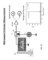
- This RF or microwave output signal can be further analyzed by, e.g., a spectrum analyzer or an oscilloscope.
- the magnetic spin-torque structure, the DC bias current and the bias magnetic field are configured to control a magnetic precession in the magnetic spin-torque structure to convert the DC bias current into an RF or microwave oscillation signal and effectuate a negative spin torque feedback to render a coupling between amplitude and phase fluctuations of the RF or microwave oscillation signal to be nearly zero.
- FIG. 1C illustrates an example of a multi-layer structure of a spin torque nano-oscillator as one implementation of the STNO device design in FIG. 1A .
- the multi-layer structure includes a substrate and a magnetic spin-torque structure formed on the substrate and structured to include a multi-layer stack of layers on the substrate in a layer configuration of Py(5)/Cu(120)/Py(5)/Cu(12)/Py(2)/Cu(2)/Pt(30) where the bottom electrode is Py(5)/Cu(120), the free layer is a thin Py(5) layer, the spacer is Cu(12), the reference layer is Py(20) and the top electrode layer is Cu(2)/Pt(30).
- the stack can be shaped to have an in-plane anisotropy such as an elliptical shape and the RL layer can be vertically tapered to achieve a material structure for the desired STNO operation.
- the STNO device can be operated to generate a tunable RF or microwave oscillation signal from the magnetic spin-torque structure.
- This structure includes a multi-layer stack of layers including a magnetic free layer and a magnetic reference layer spaced from each other and shaped to have a shape anisotropy to exhibit a spin-torque effect and a magnetic precession in the magnetic spin-torque structure under a bias magnetic field.
- the method includes applying a DC bias current to flow through the magnetic spin-torque structure; applying a bias magnetic field to the magnetic spin-torque structure to include a bias magnetic field component that is in a plane of the magnetic free layer and perpendicular to an elongated direction of the magnetic free layer; and controlling the DC bias current and the bias magnetic field to control a magnetic precession in the magnetic spin-torque structure to convert the DC bias current into an RF or microwave oscillation signal and to reduce a coupling between an amplitude and an oscillation frequency of the RF or microwave oscillation signal.
- Either or both of the DC bias current and the bias magnetic field can be controlled to set the STNO in a desired operating condition where the coupling between the amplitude and the oscillation frequency of the RF or microwave oscillation signal is reduced to a tolerable level or minimized so that the oscillator behaves like a quasi linear oscillator.
- either or both of the DC bias current and the bias magnetic field can be controlled to increase the power of the RF or microwave signal.
- either or both of the DC bias current and the bias magnetic field can be controlled to tune the oscillation frequency of the RF or microwave signal.
- the STNO device in FIG. 1A can be operated as an RF or microwave signal generator as described above.
- the STNO device in FIG. 1A can be used as a magnetic sensor where a change in the bias magnetic field at the magnetic spin-torque structure can be reflected in a change in the produced RF or microwave signal. This change in the produced RF or microwave signal, in turn, can be used to infer the change in the bias magnetic field.
- the magnetic bias module in FIG. 1A is used to produce a magnetic bias field and the combination of the DC current and this magnetic bias field sets the STNO in a desired sensing operating condition.
- the STNO device is exposed to an external magnetic field to be measured. This external magnetic field and the magnetic bias field collectively form the total bias magnetic field experienced by the STNO device.
- the STNO device can be operated as a magnetic sensor to measure a change in a magnetic field by measuring a change in the RF or microwave signal.
- LLGS Landau-Lifshitz-Gilbert-Slonczewski
- NLAO non-linear auto-oscillator
- One of approaches to achieving a quasi-linear STNO is to also increase the dynamic effective damping ⁇ eff ′ ⁇ 1 GHz. This can be obtained by employing a magnetic structure such that the variation of STNO power with I above oscillation onset is much weaker than in a typical STNO.
- the effective dynamic damping of a STNO can be expressed as
- H y in the range that provides an approximate balance between the oscillator power dependence of the red-shift due to the out-of-plane demagnetization field and that of the blue-shift due to the in-plane anisotropy field such that
- This geometry results in a significant out of plane magnetization component in the bottom two end regions of the elliptical RL, which as discussed below modifies the effective of the spin torque across the FL.
- I ⁇ 0 current bias
- PSD's power spectral densities
- the measured f exhibits a weak red-shift with I, ⁇ f/ ⁇
- this STNO device exhibits a broad range of field bias where ⁇ f can be quite low, in comparison to most previous room temperature spin valve STNO results, and still be frequency tunable
- FIG. 3 a shows a plot of I c vs. H y , as determined by the point where the oscillator mode is first clearly established, along with the value of ⁇ o for each H y as indicated by the fit of the predicted variation of I c .
- FIG. 3 b shows a plot of ⁇ f ⁇ p as determined from the measured data of FIGS. 2 b - d for the three different field values.
- I bias current
- ⁇ 1) STNO behavior that is obtained over a rather broad range of field and current in the optimum field bias regime as illustrated by the inset of FIG. 3 d is caused by a combination of a reduced agility,
- the lower N′ arises from the fact that for an in-plane magnetized FL with a significant H k such that 145°> ⁇ o >90° the strong red shift with oscillator power due to the out-of-plane demagnetization field can be substantially balanced by a blue shift resulting from H k .
- N meas ′ ranges between ⁇ 4 GHz for 700 Oe ⁇ H y ⁇ 900 Oe, yet in general
- ⁇ eff ⁇ (2 ⁇ ) ⁇ 1 ⁇ (p, I)/ ⁇ p ( ⁇ 0 /2R ⁇ I)( ⁇ p/ ⁇ I) ⁇ 1 of our STNO device in this field range that arises from its non-uniform magnetic configuration.
- ⁇ o ⁇ 10° in the in-plane orientation of the magnetization across the FL relative to that of the RL (see inset of FIG. 4 b ), which results in approximately a factor of two variation in the spin torque efficiency and hence the critical current density J c for the onset of ST oscillation between the FL ends and center for H y >700 Oe (see FIG. 4 b ).
- FIG. 4 d also shows the power restoration rate ⁇ p ′ ⁇ p ⁇ eff ′ that characterizes the dynamic damping of a STNO.
- ⁇ p ′ ranges from 0.3 ns ⁇ 1 to 0.02 ns ⁇ 1 . This rapid relaxation of power fluctuations is the result of the very strong ⁇ eff ′ in our device configuration despite its relatively low power p.
- H k shape anisotropy field
- Dynamic (I ⁇ 0) simulations include effects from magnetic interactions between the two layers and the Oersted field due to I.
- ⁇ eff ′ ⁇ o 2 ⁇ ⁇ ⁇ ⁇ I ⁇ ( ⁇ p ⁇ I ) - 1
- ⁇ ⁇ v 2 ⁇ ⁇ ⁇ ⁇ I ⁇ o ⁇ ( ⁇ f ⁇ I ) .
- Micromagnetic calculations were used in our simulations to compute by the energy minimization method the internal field distribution ( ⁇ right arrow over (H) ⁇ int ( ⁇ right arrow over (r) ⁇ )) for our STNO device under an external field H y .
- the modeled multilayer structure had a tapered elliptical shape with a sidewall taper of 20° and with cross-sectional dimensions of 50 ⁇ 150 nm 2 at the bottom of the nanopillar stack.
- the modeling digitized the volume into 2.5 ⁇ 2.5 ⁇ 2.5 nm 3 unit cells. Starting from the bottom the multilayer consisted of Py(5)/Cu(12.5)/Py(20), with the thickness in nm.
- the internal field determines the “natural” oscillation frequency of each element of the FL at the onset of oscillation, and hence, given the limited strength of the exchange coupling between the elements, the width and character of this distribution provides a measure of the tendency of the FL to have multiple, spatially distributed, modes of oscillation as opposed to exhibiting a single, more or less spatially uniform oscillation when the distribution is sufficiently narrow.
- ⁇ right arrow over (H) ⁇ int ( ⁇ right arrow over (r) ⁇ ) of the FL of a spin value nanopillar has a spatial non-uniformity, with both its local average and dispersion being strongly dependent on the location and H y .
- To quantify the topographical inhomogeneity of ⁇ right arrow over (H) ⁇ int ( ⁇ right arrow over (r) ⁇ ) in our structure we employed two different methods.
- FIG. 5 a shows that there is a significant difference in the averages of
- / ⁇ drN(r)) ⁇ where C(r) ⁇
- r dr′′dr′ is the normalization function.
- a (H y ) provides a quantitative, weighted measure of the spatial non-uniformity in ⁇ right arrow over (H) ⁇ int ( ⁇ right arrow over (r) ⁇ ) as the function of the hard axis bias. As shown in FIG. 5 b , A (H y ) decreases markedly, by more than a factor of six as H y is increased to ⁇ 700 Oe, and reaches its minimum value at ⁇ 1000 Oe. Thus both approaches indicate that the internal field distribution is much more uniform when H y is in the 700 to 1000 Oe than at lower bias fields, consistent with view that a relatively uniform internal field distribution will result in single mode behavior in a STNO.
- the magnetoresistance voltage signal is ⁇ V(t) ⁇ I ⁇ ( ⁇ R/ ⁇
- ⁇ is the gyromagnetic ratio
- H k is the anisotropy field of the FL along the easy axis
- H d is the dipole field from the RL
- H y is the externally applied hard axis magnetic field
- g( ⁇ ) 1 ⁇ 2
- the spin-polarization P 0.37.
- ⁇ FL Rotate the FL moment towards the hard axis.
- a ⁇ circumflex over (z) ⁇ out-of-plane spin polarization acts to increase the onset current I c and, if sufficiently strong can completely suppress the onset of ST oscillation as in the ⁇ 15° case illustrated in FIGS.
- the suggested approach is to apply an external field with a substantial hard axis component so that the red shift due to the power dependence of the oscillation frequency from the out-of-plane demagnetization field is balanced by the blue shift arising from the in-plane anisotropy field.
- Analysis treating the FL as a rigid domain, or alternatively macrospin modeling, can provide understanding of the origin of the reduced agility, and some general guidance as to what field configuration to employ to achieve it.
- H d 250 Oe this result predicts a transition from a red shift, N′ ⁇ 0, to a blue shift, N′>0, at H y ⁇ 600 Oe ( FIG. 5 b ), which is somewhat below the experimentally observed transition point, H y ⁇ 750 Oe, that depends weakly on I dc ( FIG. 3 d ).
- FIG. 3 d and FIG. 7 show that while the macrospin approximation provides a general understanding of the cross-over between red shift and blue shift behavior as H y is increased, even full macrospin modeling gives only an approximate indication of the variation of the agility as the function of applied fields in the non-collinear case. This is attributable to the non-uniform nature of the magnetization of the FL in this field regime that requires micromagnetics to fully model and, if desired, to provide more precise guidance as the field bias that will minimize N′.
- the end regions remain more rotated towards the hard axis than the center at the “easy axis' extrema of the oscillation (first panel).
- the magnetization of the end regions reaches the hard axis direction before the center region.
- the hard axis extrema of the oscillation occurs when the FL is more or less uniform in the hard axis direction (panel 3 ).
- the FL magnetization then moves away from this point in a non-uniform manner with the center region leading and the end regions lagging (panel 4 ).
- the simulations also indicate that there is a smaller ST oscillation in the magnetization of the bottom of the RL which is largely concentrated in the end regions and which acts to enhance the ST damping of the FL end regions.
- micromagnetic simulations also serve to demonstrate the beneficial effect of the out-of-plane magnetization in the end regions the RL in promoting a more coherent mode of FL oscillation particularly at the higher bias currents.
- the in-plane effective ST field that arises from the perpendicular spin current component acts to counter-balance the circumferential Oersted field generated by the bias current in the end regions as illustrated in FIG. 8 .
- H ST ip ⁇ 15 Oe/mA assuming ⁇ RL ⁇ 12° as determined by averaging the modeled RL magnetization over several end region cells.
- H ST ip depends on the local out-of-plane orientation of the RL magnetization ⁇ RL , the current polarization P, and the angular dependence of the spin torque function g( ⁇ ) an even closer balance of the Oersted and ST fields might be achievable with careful tuning of the device geometry (taper) and choice of material.
- FIGS. 9 a and 9 b illustrate the in-plane shape in a top view and the shape of the layers along the vertical direction perpendicular to the layers.
- the bottom Py(5) layer was used to promote adhesion and played no significant magnetic or electrical role.
- the nanopillar devices patterned by electron-beam lithography and Ar ion milling, had an elliptical cross-sectional area of ⁇ 50 ⁇ 145 nm 2 at the bottom of the nanopillar, as measured by scanning electron microscopy ( ⁇ 5 nm).
- the thinner FL is located closer to the substrate than the thicker ferromagnetic reference layer (RL) and hence the RL has a higher aspect ratio than the FL due to the sidewall tapering (20°-30° from vertical) during the ion-mill process.
- FIG. 9 b A schematic illustration of the tapered geometry is provided in FIG. 9 b .
- H k shape anisotropy field
- H y ⁇ 1000 Oe an in-plane hard axis magnetic field
- FL oscillations are generated for I ⁇ 0 such that electrons flow from the RL to the FL.
- An important aspect of this tapered spin valve structure is that the magnetization at the bottom of the RL is distinctly non-uniform, due to demagnetization field effects as indicated by the micromagnetic static simulation result shown in FIG. 9 b . As such, the orientation of the polarization of the spin current that impinges on the FL has a substantial spatial variation across the FL.
- PSDs power spectral densities
- the measured ⁇ f goes through broad minima as a function of
- (see the H y 700 Oe curve in FIG. 10 d ) with the lowest RT linewidths ⁇ f ⁇ 5 MHz.
- FIG. 10 b shows that for H y between 700 and 880 Oe, the oscillation f undergoes a crossover from a red shift with
- the bias region where low values of ⁇ f are obtained is associated with relatively small values of df/d
- We converted the measured P L to p 0 using the simplifying assumption that the FL moment is precessing in a parabolic potential and hence that p 0 sin 2 ( ⁇ /2).
- FIG. 11 a shows a plot of I c vs. H y , where I c is determined by extrapolation of p N ⁇ 1 to zero in the sub-threshold regime, along with the value of ⁇ o for each H y as indicated by the fit to the predicted variation of I c .
- I c is determined by extrapolation of p N ⁇ 1 to zero in the sub-threshold regime, along with the value of ⁇ o for each H y as indicated by the fit to the predicted variation of I c .
- FIG. 11 b shows a plot of ⁇ f ⁇ p o as determined in this manner from the measured data of FIG. 10 b - d .
- H y increases from 600 Oe ⁇ meas decreases rapidly, reaching its minimum ⁇ 5 MHz at H y opt ⁇ 700 Oe, and then increases again with higher H y , while p o decreases monotonically.
- FIG. 11 d is the NLAO prediction ⁇ f pred , as determined from Eqs. (1) and (3) using the estimated values of p o and the measured values of I df/dI.
- the NLAO model can be used to determine ⁇ using Eq. (3), obtaining the results shown in FIG. 12 b .
- ⁇ 1) can be obtained in such an STNO device over a significant range of H y and I.
- FIG. 12 b suggests that the STNO can be operated under a range of Hy between 700 Oe and 800 Oe to achieve the quasi-linear behavior (
- N/2 ⁇ df/dp 0 using the measured values of f and the estimated values of p 0 and by evaluating ⁇ eff /2 ⁇ from Eq. (3) ( FIG.
- the power restoration rate ⁇ p ⁇ p ⁇ eff characterizes the dynamic damping of a STNO. As shown in FIG. 12 d , for the device discussed in the main text ⁇ p /2 ⁇ ranges from 0.3 ns ⁇ 1 to 0.02 ns ⁇ 1 for 600 Oe ⁇ H y ⁇ 850 Oe. This rapid relaxation of power fluctuations is the result of the very strong ⁇ eff in our device configuration despite its relatively low power p.
- the power of the STNO oscillation signal exhibits a sensitive increase region in the current range of ⁇ 2 mA to ⁇ 3 mA and shows a power saturation when the current increases beyond ⁇ 3 mA where the rate of the power increase begins to decrease beyond ⁇ 3 mA.
- the MMS suggests that this OPM plays a significant role in the dynamics because the current incident on the FL end regions has a significant out-of-plane polarization (OPP) component that acts to induce the magnetization of the right (left) FL end region to have a significant time-averaged +z ( ⁇ z) component.
- OPM out-of-plane polarization
- the MMS indicates that this phase difference reduces the overall efficiency of the in-plane ST for a given I (reduces the oscillation energy) in comparison to a fully in-phase case, and thus raises I c in comparison to that predicted for a rigid domain and retards the growth of p (oscillation amplitude ⁇ ) with I just above I c (enhances ⁇ eff ).
- This results in the in-plane precession in the right end region leading (lagging) that in the left end during the half cycle for which the time-varying demagnetization field in that end is enhanced (reduced) by the effect of the OP ST. Since the OP ST and IP ST increase together with I, the result at first is a slower than otherwise expected rate of increase of p 0 with I, and hence a higher effective dynamic damping of the oscillation (see FIG. 14 for I ⁇ 2.25 mA).
- the MMS indicates that once ⁇ varies to below 90° during the oscillation the “back-action” ST exerted on the RL by the anti-parallel spin-polarized electrons reflected from the FL is sufficient, due to the lowered demagnetization field in the end regions of the RL, to set those regions into significant precession about their local effective fields that point partially out of plane, thus periodically increasing and decreasing the OPP of the current incident on the FL.
- the MMS indicates that this makes the large-amplitude in-plane FL precession less uniform across the FL, which strongly reduces the efficiency of the IP ST (See FIG. 16 ).
- the effect is a strong enhancement of ⁇ eff for
- the micromagnetic simulations further serve to demonstrate an additional beneficial effect of the OPM component at the bottom ends of the RL, in that it also aids in the achievement of coherent quasi-uniform oscillations, particularly at the higher bias currents.
- the orthogonal, out-of-plane component of the spin current incident on the FL not only acts to produce time-averaged out-of-plane components of the free layer magnetization, M z,L ⁇ 0 and M z,R >0 at the left and right ends respectively, it also has the effect of exerting a torque on the FL magnetization in those end regions that, to first order, is equivalent to the presence of an effective magnetic field,
- the OPP component of the incident spin polarization not only results in the enhanced nonlinear dynamic damping, it also allows for the application of a higher bias current, hence the achievement of a higher p 0 , before nonlinear effects lead to the onset of multiple modes.
- H st ip depends on the local out-of-plane orientation of the RL magnetization ⁇ RL , the current polarization P, and the angular dependence of the spin torque function g( ⁇ ) an even closer balance of the Oersted and ST fields might be achievable with careful tuning of the device geometry (taper) and choice of material.
- the maximum normalized power is relatively low, p o ⁇ 0.08. This helps ensure that the oscillating FL does not have sufficient energy to break up into multiple modes in the presence of the spatially non-uniform anti-damping and damping spin torques and a non-uniform internal field distribution, but it also limits the minimum attainable quasi-linear ⁇ f. Further refinements that both utilize this non-linear effective damping approach can be expected to result in a quasi-linear STNO that can reach normalized power levels, p o >>0.1, before being saturated by the negative feedback damping. This, and/or the use of a FL with a higher magnetic moment and hence greater possible STNO energy, would yield STNOs with ⁇ f ⁇ 1 MHz. Implementation of this non-linear effective damping approach in magnetic tunnel junction STNOs, and with configurations that do not require external fields, have the potential of further advancing STNOs towards viability for technological applications.
- the disclosed technology relates to spin-torque excited nanoscale oscillators where a spin-polarized electrical current, or alternatively a pure spin current, excites a nanoscale magnetic element or magnetic domain into persistent magnetic oscillation at a microwave frequency set by the magnetization of the element and the effective internal magnetic field. More specifically, the disclosed technology includes a method and system whereby the inherently non-linear nature of a spin torque nano-oscillator, which leads to an adverse coupling of amplitude and phase fluctuations that degrades the phrase stability of the oscillator, can be greatly reduced and even effectively eliminated by an internal spin torque mechanism that introduces intrinsic negative feedback of power fluctuations into the device operation.
- a spin torque nanoscale oscillator can be configured as a compact electronic device having a thin film ferromagnetic nanostructure or extended layer where the magnetization of this ferromagnetic element is locally excited into magnetic oscillation by what is referred to as an anti-damping spin transfer torque that is exerted by a spin-polarized current of electrons that impinges on the ferromagnetic element.
- This spin polarized current can be produced by passing an electrical current through one or more, but at least one, magnetically stable thin film ferromagnetic layer(s) that is (are) placed adjacent to the excited ferromagnetic element, but separated from it by a thin normal metal layer or by a very thin, tunnel barrier layer, such as for example magnesium oxide (MgO), that facilitates the tunneling of spin polarized electrons from the stable ferromagnetic element or elements to the excited element.
- MgO magnesium oxide
- the magnetic stability of the second ferromagnetic element, and possibly a third or more, is achieved by virtue it being, for example, either thicker and hence more difficult to excite by the transfer of spin torque from the current, or by being in contact with an anti-ferromagnetic layer that acts to pin its magnetization in a preferred direction.
- This magnetic stability of the other ferromagnetic components does not have to be complete as some smaller, sympathetic magnetic oscillations within the other layers can be beneficial to the overall oscillator performance.
- the required spin polarized current of electrons can be generated by the spin Hall effect wherein a longitudinal electrical current flowing through a “spin Hall material” layer, which is a high atomic number normal metal thin film layer, such as Ta or W or some other metal layer in which the conduction electrons have a strong spin orbit interaction, generates a transverse current of spin-polarized electrons that impinges onto and can excite magnetic oscillations in a ferromagnetic element that is placed adjacent to and in electrical contact with the spin Hall material.
- spin Hall material is a high atomic number normal metal thin film layer, such as Ta or W or some other metal layer in which the conduction electrons have a strong spin orbit interaction
- the magnetic excitation of the ferromagnetic element arises via the process known as spin transfer thereby the majority of the net transverse component of the spin angular momentum of the spin polarized electrons that impinge onto that ferromagnetic element is absorbed by the element's magnetic moment, which has the effect of exerting a magnetic torque on that moment.
- this torque acts to oppose, or if in the opposite direction, to enhance the so-called damping torque that relaxes magnetic excitations in ferromagnetic elements back to equilibrium.
- the spin transfer torque is in the direction to oppose the damping torque it is referred to as an “anti-damping spin torque.”
- the polarized spin current density is high enough the anti-damping spin torque can exceed the damping torque.
- the element will be set into persistent magnetic oscillation, provided the magnetic moment upon excitation cannot move into an alternative magnetic configuration where the spin torque becomes a damping torque and suppresses excitations.
- this magnetic reversal is avoided by placing the ferromagnetic element in a net internal magnetic field configuration that only allows for one stable, equilibrium point. (For magnetic memory applications a magnetically bi-stable configuration is established, which can result in reversible spin transfer torque switching of the magnetic moment orientation between the two stable configurations.)
- the principal practical value of STNOs is that the magnetic oscillation can be employed to generate an electromagnetic signal at either the fundamental or a harmonic of the frequency of that oscillation.
- This is possible because of the change in resistance, known as the magnetoresistance, which develops between the oscillating element and an adjacent fixed ferromagnetic element that depends on the instantaneous relative magnetic orientation of the fixed element to that of the oscillating element.
- This magnetoresistance is that experienced by either an electrical current flowing between the two ferromagnetic elements, through a thin normal metal layer, or by an electrical current that quantum mechanically tunnels through a very thin insulator layer, such a magnesium oxide or some other insulating material of order of 1 nm in thickness, that is inserted between those two ferromagnetic elements.
- a variety of nanoscale device geometries have been employed to produce STNOs.
- Approaches include mechanical point contacts, nanopillar spin valve structures, nanoconstrictions that contact extended magnetic multilayer films and nanoscale magnetic tunnel junctions (MTJs).
- the oscillating magnetic element has been either a fully patterned nanoscale thin film layer, or the localized region of an extended ferromagnetic film surrounding the area into which a polarized spin current is injected.
- the mode of magnetic oscillation can vary from being the precession of a more or less uniformly magnetized region of the excited magnetic element about its equilibrium position set by the internal magnetic fields, to, for example, the precession of a magnetic vortex in the thin film element about its equilibrium position.
- the frequency (frequencies) of a STNO's mode (modes) of oscillation is (are) determined by the saturation magnetization of the excited ferromagnetic element and by the internal magnetic field distribution associated with that mode of excitation.
- a STNO should have only one dominant mode of oscillation, which depending on the internal field and magnetization of the excited ferromagnetic element, can range from below 0.5 GHZ to greater than 20 GHz, but most commonly, STNO operating frequencies fall within the 0.5-20 GHz range, which covers most of the electromagnetic spectrum utilized for public and commercial communications.
- a fundamental performance parameter of any electromagnetic oscillator is its phase stability, or spectral linewidth ( ⁇ f).
- phase stability or spectral linewidth ( ⁇ f).
- ⁇ f spectral linewidth
- the oscillator's magnetic energy is not the same as the device's microwave output power as the latter also depends on the characteristics of the magnetoresistance sensor. Increasing the volume of the oscillating magnetic region to achieve higher oscillator energy offers only a limited solution to increasing phase stability since achieving a single mode of oscillation requires that the lateral extent of the magnetic element be less than that required to energetically support a domain wall, which is typically on the order of 100 nm for most STNO ferromagnetic materials. There is also a limit to the achievable amplitude of a STNO oscillation, as too high an energy density will result in secondary modes of oscillation becoming energetically favorable, which will degrade performance.
- the frequency of a STNO varies with its oscillation amplitude, or normalized power, which in turn varies with the strength of the applied spin polarized current, most typically in a more or less linear manner above the threshold current that initiates the oscillator.
- This STNO “agility,” that is the variation of its frequency with oscillator power, is seemingly an attractive feature for many potential applications, but it also results in the STNOs being non-linear, in that its amplitude fluctuations result in frequency fluctuations. This directly degrades STNO phase stability, increasing its linewidth above the intrinsic limit for a linear oscillator set by thermal fluctuations.
- the disclosed technology creates a method by which strongly non-linear effective damping of STNO amplitude fluctuations is produced and employed to greatly reduce if not completely eliminate the non-linear coupling between such amplitude fluctuations and the STNO phase.
- the result is a STNO with greatly increased phase stability over previous STNO designs.
- This disclosed technology embodied through the application of any one of a variety of means of applying a spatially non-uniform spin torque to the active, magnetically oscillating element in the STNO device.
- the effect of this non-uniform spin torque is first to excite the magnetic element through the transfer of spin angular momentum from an incident spin-polarized current, or alternatively from a pure spin current generated by the spin Hall effect, or some other means.
- This spin transfer provides an anti-damping torque to the element and at sufficiently strong current levels excites it into persistent magnetic oscillation. These oscillations are converted into electromagnetic signals through a magnetoresistance effect. Once the oscillation amplitude becomes large enough the spatial variation in the polarization direction of the incident spin polarized current, or pure spin current, is such that some portion of the oscillating element locally encounters a diminishing efficiency of anti-damping spin torque with increasing oscillation amplitude, or even experiences a damping spin torque that increases in strength with increasing oscillation amplitude. This has the effect of providing negative feedback to the oscillation, strongly suppressing power fluctuations and hence greatly enhancing the non-linear effective damping of the STNO oscillation power which reduces the non-linear coupling between amplitude and phase.
- the STNO When the non-linear effective damping is sufficiently strong, which is a level that depends on the spatially dependent details of the magnetic configuration of the oscillating element relative to the spatial distribution of the incident spin polarized current, or the incident spin current, the STNO can become quasi-linear with its phase stability, or equivalently, its intrinsic oscillation linewidth, very close to the limit set by fundamental thermal fluctuations, which is determined by the ratio of the oscillation time-averaged energy to the energy provided by random thermal impulses.
- the disclosed technology realizes a non-linear response of the oscillation power of a spin torque nanoscale oscillator (STNO) to changes in the steady (dc) spin-polarized bias current, or alternatively to a pure spin bias current, that excites the steady-state oscillation, this non-linear response is such that the variation of power p 0 with bias current I above some value becomes sufficiently low so as to achieve an enhancement of the non-linear effective damping ⁇ eff ⁇ 0 I/(dp 0 /dI) of the STNO.
- STNO spin torque nanoscale oscillator
- This enhanced non-linear effective damping provides negative feedback to the oscillating element, suppressing oscillator power fluctuations and thereby substantially reducing the non-linear coupling constant ⁇ , potentially to ⁇ 1 such that the spectral linewidth of the oscillator, or equivalently its phase stability, can be close to the fundamental limit set by intrinsic thermal fluctuations.
- the disclosed technology implements the general method whereby once the amplitude of the magnetic oscillation reaches a certain level, further increases in oscillation amplitude result in a reduction of the net effectiveness of the spin torque applied to the oscillating element.
- a fluctuation to a higher amplitude of oscillation results in a negative feedback where the power of the oscillator is quickly reduced due to the reduced overall efficiency of the overall applied anti-damping spin torque.
- a fluctuation in oscillator amplitude to a lower level results in a significantly increased efficiency of the applied spin torque, which results in the oscillator amplitude being quickly restored to the higher, steady state level.
- This negative feedback of power fluctuations provides the non-linear effective damping that together with a reasonable level of oscillator agility results in a quasi-linear STNO with greatly improved spectral linewidth, or equivalently phase stability.
- the disclosed technology employs an anti-damping spin torque that is strongly and non-linearly dependent on oscillation amplitude to provide negative feedback and thus suppress power fluctuations in a STNO.
- the disclosed technology includes employing internal negative feedback during the excitation of a STNO is implemented by the provision of a substantial spatial variation in the strength of the anti-damping spin-transfer torque that is exerted on the magnetically oscillating element by the incident spin polarized current or the pure spin current. Due to this spatial variation some region (regions) of the magnetically oscillating element receives (receive) a relatively strong excitation while another region (other regions) of the magnetically oscillating element receives a spin transfer torque that either diminishes in strength with oscillation amplitude, or due to the time-averaged orientation of the local magnetization relative to the polarization direction of the incident current receives a spin torque that has a positive damping effect once the overall oscillation power reaches a certain level. This can occur because the effectiveness or efficiency of spin transfer for generating anti-damping varies with the angle ⁇ 0 between the axis of precession and the direction of the incident net spin polarization.
- the anti-damping effectiveness of this spin torque in exciting persistent magnetic oscillation is ⁇ d ⁇ st /d ⁇ 0 ⁇ st (0)cos ⁇ 0
- the angle ⁇ 0 is the angle between the direction of polarization of incident spin polarized current, or of the incident spin current, and the average, midpoint, orientation of the magnetization of the ferromagnetic element that is excited.
- This spatially varying spin torque is utilized in the disclosed technology by establishing a device configuration where ⁇ 0 varies substantially across the excited element, such that in some area (areas) ⁇ 0 >>90° and in another area (other areas) it is decreased to ⁇ 0 :90° or less.
- the magnetic exchange interaction in a ferromagnetic material in general couples, to a degree quantified by the amplitude of an exchange coupling constant J, adjacent ionic magnetic moments such that a rotational displacement of one moment from its equilibrium magnetic orientation results in a torque being applied to the neighboring moments that acts to induce a similar rotation as that of the first moment.
- This non-linear enhanced effective damping can be further increased if the orientation of the axis of precession ⁇ 0 decreases with the amplitude of the applied bias current, d ⁇ 0 /dI ⁇ 0. This is generally the case if the magnetic configuration is such that over at least some region of the oscillating element the orientation is such that 90° ⁇ 0 ⁇ 180° before the application of the spin polarized bias current.
- a decrease in ⁇ 0 with increased bias current is equivalent to a decrease in spin torque effectiveness with increasing oscillation amplitude (power), and this provides enhanced effective damping that suppresses power fluctuations.
- the disclosed technology can be embodied in any one of a number of ways.
- the disclosed technology includes a magnetic spin valve structure.
- this spin polarized current passes through a normal metal conducting layer, such a Cu, and impinges onto a second, thinner ferromagnetic layer, referred to as the “free layer” (FL), the absorption of the spin angular momentum that is transverse to the local magnetization orientation of the free layer exerts a torque on the free layer.
- FL normal metal conducting layer
- this torque has the effect of opposing the intrinsic magnetic torque that causes damping of any magnetic excitation in the free layer, that is, the absorption of the transverse spin angular momentum has the effect of an “anti-damping” torque.
- the incident spin polarized current is sufficiently large the free layer is excited into persistent magnetic oscillation by this spin torque.
- the steady state amplitude of this persistent oscillation is determined by the time-averaged balance between the magnetic damping and the anti-damping, with the total time-averaged damping, that is the sum of the positive damping torque and the negative anti-damping, being zero.
- the magnetic oscillation is detected in this embodiment of the disclosed technology by the magneto-resistance of the spin valve structure where the electrical resistance to current flow between the two ferromagnetic layers depends on the relative orientation of the local magnetizations of the two layers opposite each other.
Abstract
Description
where E is the time averaged energy of the oscillator, Γo=αG·γ·2πMs, Ms is the saturation magnetization of the oscillating magnetic free layer (FL), p (≦1) is the normalized oscillator power, f is the frequency, V is the FL volume, αG is the Gilbert damping parameter, kB is the Boltzmann constant, T is the temperature, γ is the electron gyromagnetic ratio. In general the nonlinear coupling factor (ν) is given by
where N′≡∂f/∂p is the agility of the STNO, and where the total damping Γ(p, I)=Γ+(p)−Γ−(p, I), which is zero during steady state oscillation, is the difference between the natural positive (dissipative) damping Γ+(p)=Γo(1+η/(p))≈Γo, (neglecting any power dependence of the positive damping, i.e. assuming η(p)<<1), and the negative damping Γ−(p, I)=σI caused by τST. Here σ=σ0g(p) is the anti-damping effectiveness of the spin-polarized current with g(p) representing its power dependence (g(0)=1). In general σ0=Γ0/Ic, where Ic is the current required for oscillation onset.
In combination with an in-plane bias magnetic field Hy in the range that provides an approximate balance between the oscillator power dependence of the red-shift due to the out-of-plane demagnetization field and that of the blue-shift due to the in-plane anisotropy field such that |N′|<4 GHz, a small I ∂p/∂I and hence large Γeff′˜2-6 GHz will result |ν|≦1.
in the end regions, where {right arrow over (p)} is the spin-polarization of the RL and θRL is the out-of-plane angle of that polarization (see
Γ(I,p)|p=p
and using Eq. S3, the following equations can be obtained:
Here γ is the gyromagnetic ratio, m=(mx,my,mz) is the unit vector of the FL, Hk is the anisotropy field of the FL along the easy axis, Hd is the dipole field from the RL, Hy is the externally applied hard axis magnetic field, g(θ)=½, and the spin-polarization P=0.37. With Eq. S7 we obtained m(t) and from this time dependence of the rigid FL moment we determined its precessional axis (φFL and θFL) and p=sin2(ε/2) as the function of I, Hy and Hd for Hk=450 Oe, where φFL is the in-plane orientation of the FL as measured from −{circumflex over (x)}, θFL is its out-of-plane tilt angle and e is the maximum in-plane precessional excursion angle (see
E(φ,θ)=−H d M s cos θ cos φ−H y M s cos θ sin φ−(H k M s/2)cos2 θ cos2 φ+2πM s 2 sin2 θ
where θ is the out-of-plane tilt angle of the FL moment. At equilibrium ({right arrow over (m)}//{right arrow over (H)}) the FL lies in-plane and we have: (Hk−H)cos φo=H and H sin φo=Hy
-
- (S8), where His the effective in-plane internal field. The ferromagnetic resonance frequency of the FL is then ωo 2≈γ2[H−Hk sin2 φo][H+4πMs cos2 θ]θ=0°
- (S9), and thus ωo is determined by the effective in-plane anisotropy field (Hk,eff=Hk sin2 φ) and the out-of-plane demagnetization field (4πMeff=4πMs cos2 θ). When the FL is ST excited, the mean oscillation frequency varies with amplitude. To examine this we assume a (small angle) in-plane precession of the FL about H (φ=φo+ε sin(ωt)), although we note that the τst also shifts the oscillation's in-plane (φo). We then have <Hk sin2 φ>≈Hk(sin2 φo+cos 2φo·4p) and 4πMeff=<4πMs·ξ·cos2(ε)>≈4πMs(1−ξ·4p) where p≡<sin2(ε/2)>≈<ε2>/4 and ξ is the ellipticity factor due to 4πMeff>>H. The time-averaged ω2 is ω2≈γ2[H−Hk(sin2 φo+cos 2φo·4p)][H+4πMs(1−ξ·4p)] and we have:
- (S8), where His the effective in-plane internal field. The ferromagnetic resonance frequency of the FL is then ωo 2≈γ2[H−Hk sin2 φo][H+4πMs cos2 θ]θ=0°
where RS is the device resistance (RS≈25Ω) and Vg is the amplitude of the generated microwave signal (ΔV(t)=Vg sin(ωt)). A correction was also made for the calculated power lost to the Si substrate. We assumed that the magnetoresistance voltage signal is ΔV(t)=I·R(t)≈I·(∂R/∂φ|φ
and φ(t)=φo+ε sin(ωt). We measured ΔRo=0.2Ω and assumed χ=1 as previously reported for a Py spin valve. We converted the measured PL to p0 using the simplifying assumption that the FL moment is precessing in a parabolic potential and hence that p0=sin2(ε/2). We find in the small power limit that
with R′(φo)=dR/dφ|φ
Claims (30)
Priority Applications (1)
| Application Number | Priority Date | Filing Date | Title |
|---|---|---|---|
| US14/760,999 US9577653B2 (en) | 2013-01-14 | 2014-01-14 | Quasi-linear spin torque nano-oscillators |
Applications Claiming Priority (3)
| Application Number | Priority Date | Filing Date | Title |
|---|---|---|---|
| US201361752430P | 2013-01-14 | 2013-01-14 | |
| PCT/US2014/011555 WO2014110603A1 (en) | 2013-01-14 | 2014-01-14 | Quasi-linear spin torque nano-oscillators |
| US14/760,999 US9577653B2 (en) | 2013-01-14 | 2014-01-14 | Quasi-linear spin torque nano-oscillators |
Publications (2)
| Publication Number | Publication Date |
|---|---|
| US20150372687A1 US20150372687A1 (en) | 2015-12-24 |
| US9577653B2 true US9577653B2 (en) | 2017-02-21 |
Family
ID=51167463
Family Applications (1)
| Application Number | Title | Priority Date | Filing Date |
|---|---|---|---|
| US14/760,999 Active US9577653B2 (en) | 2013-01-14 | 2014-01-14 | Quasi-linear spin torque nano-oscillators |
Country Status (2)
| Country | Link |
|---|---|
| US (1) | US9577653B2 (en) |
| WO (1) | WO2014110603A1 (en) |
Cited By (3)
| Publication number | Priority date | Publication date | Assignee | Title |
|---|---|---|---|---|
| RU189670U1 (en) * | 2018-12-10 | 2019-05-30 | Федеральное государственное бюджетное учреждение науки Институт физики металлов имени М.Н. Михеева Уральского отделения Российской академии наук (ИФМ УрО РАН) | Nanooscillator excited by spin current |
| US10719298B1 (en) * | 2019-02-25 | 2020-07-21 | Western Digital Technologies, Inc. | System for generating random noise with a magnetic device |
| US10879453B2 (en) * | 2016-11-02 | 2020-12-29 | Nanosc Ab | Spin oscillator device and mutually synchronized spin oscillator device arrays |
Families Citing this family (23)
| Publication number | Priority date | Publication date | Assignee | Title |
|---|---|---|---|---|
| US10468590B2 (en) | 2015-04-21 | 2019-11-05 | Spin Memory, Inc. | High annealing temperature perpendicular magnetic anisotropy structure for magnetic random access memory |
| US9728712B2 (en) | 2015-04-21 | 2017-08-08 | Spin Transfer Technologies, Inc. | Spin transfer torque structure for MRAM devices having a spin current injection capping layer |
| US9853206B2 (en) | 2015-06-16 | 2017-12-26 | Spin Transfer Technologies, Inc. | Precessional spin current structure for MRAM |
| US9773974B2 (en) | 2015-07-30 | 2017-09-26 | Spin Transfer Technologies, Inc. | Polishing stop layer(s) for processing arrays of semiconductor elements |
| US9741926B1 (en) | 2016-01-28 | 2017-08-22 | Spin Transfer Technologies, Inc. | Memory cell having magnetic tunnel junction and thermal stability enhancement layer |
| US10333058B2 (en) | 2016-03-17 | 2019-06-25 | Cornell University | Nanosecond-timescale low-error switching of 3-terminal magnetic tunnel junction circuits through dynamic in-plane-field assisted spin-hall effect |
| WO2017192986A1 (en) * | 2016-05-05 | 2017-11-09 | Arizona Board Of Regents For And On Behalf Of Arizona State University | Phase-locked spin torque oscillator array |
| US10110165B2 (en) | 2016-05-19 | 2018-10-23 | Seagate Technology Llc | Solid state microwave generator |
| US10601368B2 (en) * | 2016-05-19 | 2020-03-24 | Seagate Technology Llc | Solid state microwave generator |
| US9734850B1 (en) | 2016-06-28 | 2017-08-15 | Western Digital Technologies, Inc. | Magnetic tunnel junction (MTJ) free layer damping reduction |
| US10672976B2 (en) | 2017-02-28 | 2020-06-02 | Spin Memory, Inc. | Precessional spin current structure with high in-plane magnetization for MRAM |
| US10665777B2 (en) | 2017-02-28 | 2020-05-26 | Spin Memory, Inc. | Precessional spin current structure with non-magnetic insertion layer for MRAM |
| US10360961B1 (en) | 2017-12-29 | 2019-07-23 | Spin Memory, Inc. | AC current pre-charge write-assist in orthogonal STT-MRAM |
| US10270027B1 (en) * | 2017-12-29 | 2019-04-23 | Spin Memory, Inc. | Self-generating AC current assist in orthogonal STT-MRAM |
| US10319900B1 (en) | 2017-12-30 | 2019-06-11 | Spin Memory, Inc. | Perpendicular magnetic tunnel junction device with precessional spin current layer having a modulated moment density |
| US10339993B1 (en) | 2017-12-30 | 2019-07-02 | Spin Memory, Inc. | Perpendicular magnetic tunnel junction device with skyrmionic assist layers for free layer switching |
| US10468588B2 (en) | 2018-01-05 | 2019-11-05 | Spin Memory, Inc. | Perpendicular magnetic tunnel junction device with skyrmionic enhancement layers for the precessional spin current magnetic layer |
| US10580827B1 (en) | 2018-11-16 | 2020-03-03 | Spin Memory, Inc. | Adjustable stabilizer/polarizer method for MRAM with enhanced stability and efficient switching |
| US10726892B2 (en) | 2018-12-06 | 2020-07-28 | Sandisk Technologies Llc | Metallic magnetic memory devices for cryogenic operation and methods of operating the same |
| CN111934625A (en) * | 2020-08-14 | 2020-11-13 | 北京航空航天大学合肥创新研究院 | Phase modulation method for spin transfer torque nanooscillator |
| CN112331763B (en) * | 2020-11-16 | 2023-11-07 | 北京航空航天大学合肥创新研究院 | Instantaneous frequency modulation method of spin nano-oscillator |
| CN113823733A (en) * | 2021-09-07 | 2021-12-21 | 北京航空航天大学合肥创新研究院(北京航空航天大学合肥研究生院) | Three-dimensional series-parallel synchronous array of spin torque oscillator, oscillator and preparation method |
| CN113768488B (en) * | 2021-09-23 | 2022-03-08 | 中国科学院自动化研究所 | Magnetic nanoparticle imaging method and system based on non-uniform excitation field |
Citations (5)
| Publication number | Priority date | Publication date | Assignee | Title |
|---|---|---|---|---|
| US20080150640A1 (en) * | 2006-10-31 | 2008-06-26 | Seagate Technology Llc | Spin oscillator device |
| US20090257274A1 (en) | 2008-04-14 | 2009-10-15 | Kiyotaro Itagaki | Semiconductor memory device |
| US20100188890A1 (en) | 2007-06-25 | 2010-07-29 | Shunsuke Fukami | Magnetoresistance effect element and magnetic random access memory |
| US20120062220A1 (en) | 2010-09-09 | 2012-03-15 | New York University | Aggregated spin-torque nano-oscillators |
| US20120154063A1 (en) | 2010-12-20 | 2012-06-21 | Nikonov Dmitri E | Spin torque oscillator having multiple fixed ferromagnetic layers or multiple free ferromagnetic layers |
-
2014
- 2014-01-14 WO PCT/US2014/011555 patent/WO2014110603A1/en active Application Filing
- 2014-01-14 US US14/760,999 patent/US9577653B2/en active Active
Patent Citations (5)
| Publication number | Priority date | Publication date | Assignee | Title |
|---|---|---|---|---|
| US20080150640A1 (en) * | 2006-10-31 | 2008-06-26 | Seagate Technology Llc | Spin oscillator device |
| US20100188890A1 (en) | 2007-06-25 | 2010-07-29 | Shunsuke Fukami | Magnetoresistance effect element and magnetic random access memory |
| US20090257274A1 (en) | 2008-04-14 | 2009-10-15 | Kiyotaro Itagaki | Semiconductor memory device |
| US20120062220A1 (en) | 2010-09-09 | 2012-03-15 | New York University | Aggregated spin-torque nano-oscillators |
| US20120154063A1 (en) | 2010-12-20 | 2012-06-21 | Nikonov Dmitri E | Spin torque oscillator having multiple fixed ferromagnetic layers or multiple free ferromagnetic layers |
Cited By (3)
| Publication number | Priority date | Publication date | Assignee | Title |
|---|---|---|---|---|
| US10879453B2 (en) * | 2016-11-02 | 2020-12-29 | Nanosc Ab | Spin oscillator device and mutually synchronized spin oscillator device arrays |
| RU189670U1 (en) * | 2018-12-10 | 2019-05-30 | Федеральное государственное бюджетное учреждение науки Институт физики металлов имени М.Н. Михеева Уральского отделения Российской академии наук (ИФМ УрО РАН) | Nanooscillator excited by spin current |
| US10719298B1 (en) * | 2019-02-25 | 2020-07-21 | Western Digital Technologies, Inc. | System for generating random noise with a magnetic device |
Also Published As
| Publication number | Publication date |
|---|---|
| US20150372687A1 (en) | 2015-12-24 |
| WO2014110603A1 (en) | 2014-07-17 |
Similar Documents
| Publication | Publication Date | Title |
|---|---|---|
| US9577653B2 (en) | Quasi-linear spin torque nano-oscillators | |
| US10847197B2 (en) | Circuits and devices based on enhanced spin Hall effect for efficient spin transfer torque | |
| US10333058B2 (en) | Nanosecond-timescale low-error switching of 3-terminal magnetic tunnel junction circuits through dynamic in-plane-field assisted spin-hall effect | |
| Houssameddine et al. | Spin-torque oscillator using a perpendicular polarizer and a planar free layer | |
| US9222994B2 (en) | Perpendicular spin torque oscillator FMR frequency measurement method | |
| Suzuki et al. | Spin-torque diode effect and its application | |
| Berkov et al. | Micromagnetic simulations of magnetization dynamics in a nanowire induced by a spin-polarized current injected via a point contact | |
| Chen et al. | Magnetic droplet mode in a vertical nanocontact-based spin hall nano-oscillator at oblique fields | |
| Finocchio et al. | Spin-torque-induced rotational dynamics of a magnetic vortex dipole | |
| Sun | Resistance-area product and size dependence of spin-torque switching efficiency in CoFeB-MgO based magnetic tunnel junctions | |
| Sluka et al. | Spin-transfer torque induced vortex dynamics in Fe/Ag/Fe nanopillars | |
| US11533020B2 (en) | Single magnetic-layer microwave oscillator | |
| Teixeira et al. | Stabilization of the easy-cone magnetic state in free layers of magnetic tunnel junctions | |
| Liu et al. | Anatomy of type-x spin-orbit-torque switching | |
| Lee et al. | Quasilinear spin-torque nano-oscillator via enhanced negative feedback of power fluctuations | |
| Baker et al. | Antidamping torques from simultaneous resonances in ferromagnet-topological insulator-ferromagnet heterostructures | |
| Liu et al. | Field-free type-x spin-orbit-torque switching by easy-axis engineering | |
| Xiao et al. | Charge pumping and the colored thermal voltage noise in spin valves | |
| Kent et al. | Magnetization dynamics | |
| Keatley et al. | Optically detected spin–orbit torque ferromagnetic resonance in an in-plane magnetized ellipse | |
| Pan et al. | All-optical investigation of anisotropic spin pumping in W/CoFeB/W heterostructure | |
| Chen et al. | Collimated Bidirectional Propagating Spin Wave Generated by a Nonlocal Spin-Current Nano-oscillator | |
| Gangmei et al. | Thermal and spin-transfer-torque excitation of precessional modes in magnetic tunnel junction nanopillars with symmetric interfaces and a thick free layer | |
| Carpentieri et al. | Spintronic oscillators based on spin-transfer torque and spin-orbit torque | |
| Rahman et al. | Thickness dependence of magnetization dynamics of an in-plane anisotropy ferromagnet under a crossed spin torque polarizer |
Legal Events
| Date | Code | Title | Description |
|---|---|---|---|
| AS | Assignment |
Owner name: CORNELL UNIVERSITY, NEW YORK Free format text: ASSIGNMENT OF ASSIGNORS INTEREST;ASSIGNORS:BUHRMAN, ROBERT A;LEE, OAKJAE;RALPH, DANIEL C;SIGNING DATES FROM 20140410 TO 20140627;REEL/FRAME:035815/0575 |
|
| AS | Assignment |
Owner name: CORNELL UNIVERSITY, NEW YORK Free format text: CORRECTIVE ASSIGNMENT TO CORRECT THE SECOND ASSIGNOR NAME PREVIOUSLY RECORDED AT REEL: 035815 FRAME: 0575. ASSIGNOR(S) HEREBY CONFIRMS THE ASSIGNMENT;ASSIGNORS:BUHRMAN, ROBERT A;LEE, OUKJAE;RALPH, DANIEL C;SIGNING DATES FROM 20140410 TO 20140627;REEL/FRAME:036092/0001 |
|
| STCF | Information on status: patent grant |
Free format text: PATENTED CASE |
|
| CC | Certificate of correction | ||
| MAFP | Maintenance fee payment |
Free format text: PAYMENT OF MAINTENANCE FEE, 4TH YR, SMALL ENTITY (ORIGINAL EVENT CODE: M2551); ENTITY STATUS OF PATENT OWNER: SMALL ENTITY Year of fee payment: 4 |