US9564375B2 - Structures and methods for extraction of device channel width - Google Patents
Structures and methods for extraction of device channel width Download PDFInfo
- Publication number
- US9564375B2 US9564375B2 US14/054,040 US201314054040A US9564375B2 US 9564375 B2 US9564375 B2 US 9564375B2 US 201314054040 A US201314054040 A US 201314054040A US 9564375 B2 US9564375 B2 US 9564375B2
- Authority
- US
- United States
- Prior art keywords
- transistors
- integrated circuits
- capacitance
- gate
- determining
- Prior art date
- Legal status (The legal status is an assumption and is not a legal conclusion. Google has not performed a legal analysis and makes no representation as to the accuracy of the status listed.)
- Expired - Fee Related, expires
Links
Images


Classifications
-
- H01L22/14—
-
- H—ELECTRICITY
- H10—SEMICONDUCTOR DEVICES; ELECTRIC SOLID-STATE DEVICES NOT OTHERWISE PROVIDED FOR
- H10P—GENERIC PROCESSES OR APPARATUS FOR THE MANUFACTURE OR TREATMENT OF DEVICES COVERED BY CLASS H10
- H10P74/00—Testing or measuring during manufacture or treatment of wafers, substrates or devices
- H10P74/20—Testing or measuring during manufacture or treatment of wafers, substrates or devices characterised by the properties tested or measured, e.g. structural or electrical properties
- H10P74/207—Electrical properties, e.g. testing or measuring of resistance, deep levels or capacitance-voltage characteristics
-
- G06F17/5063—
-
- G06F17/5068—
-
- G—PHYSICS
- G06—COMPUTING OR CALCULATING; COUNTING
- G06F—ELECTRIC DIGITAL DATA PROCESSING
- G06F30/00—Computer-aided design [CAD]
- G06F30/30—Circuit design
- G06F30/36—Circuit design at the analogue level
-
- G—PHYSICS
- G06—COMPUTING OR CALCULATING; COUNTING
- G06F—ELECTRIC DIGITAL DATA PROCESSING
- G06F30/00—Computer-aided design [CAD]
- G06F30/30—Circuit design
- G06F30/39—Circuit design at the physical level
-
- G—PHYSICS
- G01—MEASURING; TESTING
- G01B—MEASURING LENGTH, THICKNESS OR SIMILAR LINEAR DIMENSIONS; MEASURING ANGLES; MEASURING AREAS; MEASURING IRREGULARITIES OF SURFACES OR CONTOURS
- G01B2210/00—Aspects not specifically covered by any group under G01B, e.g. of wheel alignment, caliper-like sensors
- G01B2210/56—Measuring geometric parameters of semiconductor structures, e.g. profile, critical dimensions or trench depth
Definitions
- the present disclosure relates to determining transistor channel widths.
- the present disclosure is particularly applicable to determining transistor channel widths for 20 nanometer (nm) technology nodes and beyond.
- An aspect of the present disclosure is a method for electrical measurement of manufactured device channel widths.
- Another aspect of the present disclosure is design structures for extraction of manufactured device channel width through electrical measurement.
- some technical effects may be achieved in part by a method including determining effective channel widths of transistors of a plurality of integrated circuits as a function of drawn channel widths of the transistors, and determining a target channel width for a target transistor based on the effective channel widths.
- An aspect of the present disclosure include determining respective total capacitances of the plurality of integrated circuits between gate nodes and shorted source, drain, and/or substrate nodes of the transistors, and determining the effective channel widths based, at least in part, on the respective total capacitances.
- Another aspect includes transistors for each integrated circuit having a single drawn channel width, and the single drawn channel width varies between the plurality of integrated circuits.
- Another aspect includes each transistor including a gate dielectric layer, with the gate dielectric layer varying between groups of the plurality of integrated circuits.
- Additional aspects include determining overlap capacitance between the gate node and the source node and/or the drain node corresponding to the plurality of integrated circuits, and determining the effective channel widths based, at least in part, on the overlap capacitance. Additional aspects include determining respective metal line capacitances between metal lines and substrates, without gate, source, and drain contacts for the transistors, of the plurality of integrated circuits, and determining the effective channel widths based, at least in part, on the respective metal line capacitances.
- Further aspects include determining the PC end-cap or “cap” capacitance between a gate poly endcap and a substrate corresponding to the plurality of integrated circuits, determining parallel line capacitance between the gate poly endcap and trench silicide lines of any one of the plurality of integrated circuits, and determining the effective channel widths based, at least in part, on the cap capacitance and the parallel line capacitance. Further aspects include determining gate currents of the transistors of the plurality of integrated circuits, determining lengths of channels of the transistors of the plurality of integrated circuits, and determining the effective channel widths based on the gate currents and the lengths of the channels.
- an apparatus including: at least one processor, and at least one memory including computer program code for one or more programs, the at least one memory and the computer program code configured to, with the at least one processor, cause the apparatus to perform at least the following, determine effective channel widths of transistors of a plurality of integrated circuits as a function of drawn channel widths of the transistors, and determine a target channel width for a target transistor based on the effective channel widths.
- aspects include the apparatus being further caused, at least in part, to determine respective total capacitances of the plurality of integrated circuits between gate nodes and shorted source, drain, and/or substrate nodes of the transistors, and determine the effective channel widths based, at least in part, on the respective total capacitances.
- Another aspect includes transistors for each integrated circuit having a single drawn channel width, and the single drawn channel width varies between the plurality of integrated circuits.
- each transistor including a gate dielectric layer, with the gate dielectric layer varying between groups of the plurality of integrated circuits.
- aspects include the apparatus being further caused, at least in part, to: determine overlap capacitance between the gate node and the source node and/or the drain node corresponding to the plurality of integrated circuits, and determine the effective channel widths based, at least in part, on the overlap capacitance. Still another aspect includes the apparatus being further caused, at least in part, to determine respective metal line capacitances between metal lines and substrates, without gate, source, and drain contacts for the transistors, of the plurality of integrated circuits, and determine the effective channel widths based, at least in part, on the respective metal line capacitances.
- Further aspects include the apparatus being further caused, at least in part, to determine cap capacitance between a gate poly endcap and a substrate corresponding to the plurality of integrated circuits, determine parallel line capacitance between the gate poly endcap and trench silicide lines of any one of the plurality of integrated circuits, and determine the effective channel widths based, at least in part, on the cap capacitance and the parallel line capacitance. Additional aspects include the apparatus being further caused, at least in part, to determine gate currents of the transistors of the plurality of integrated circuits, determine lengths of channels of the transistors of the plurality of integrated circuits, and determine the effective channel widths based on the gate currents and the lengths of the channels.
- Another aspect of the present disclosure includes a method including determining respective total capacitances of a plurality of integrated circuits, each integrated circuit having bitcells with transistors having a uniform drawn channel width, with the drawn uniform channel width varying between the plurality of integrated circuits, determining respective metal line capacitances of the plurality of integrated circuits, determining a cap capacitance corresponding to the plurality of integrated circuits, determining parallel line capacitance of any one of the plurality of integrated circuits, and determining effective channel widths of the transistors of the plurality of integrated circuits based on the respective total capacitances, the respective metal line capacitances, the cap capacitance, and the parallel line capacitance.
- Further aspects include determining a target channel width for designing a target transistor based on the effective channel widths. Additional aspects include determining the respective total capacitances by measuring capacitance between gate nodes and shorted source, drain, and/or substrate nodes for the plurality of integrated circuits, and determining the respective metal line capacitances by measuring capacitance between metal lines and substrates without gate, source, and drain contacts of the plurality of integrated circuits. Another aspect includes determining the parallel line capacitance by measuring capacitance between the gate poly endcap and trench silicide lines for the any one of the plurality of integrated circuits.
- FIG. 1 is a flowchart of a process for electrically measuring manufactured device channel widths for determining target channel widths, in accordance with an exemplary embodiment
- FIG. 2 is a flowchart of a process for determining various capacitances of integrated circuits for determining target channel widths, in accordance with an exemplary embodiment
- FIGS. 3A and 3B schematically illustrate design structures used in the processes of FIGS. 1 and 2 , in accordance with an exemplary embodiment
- FIG. 4 is a graph of drawn transistor widths versus total capacitance for determining target channel widths, in accordance with an exemplary embodiment.
- FIG. 5 schematically illustrates a computer system for implementing the processes of FIGS. 1 and 2 , according to an exemplary embodiment.
- the present disclosure addresses and solves the current problem of changes in the channel width between the design stage and the manufacturing stage and an inability to precisely control transistor channel width attendant upon manufacturing semiconductor devices with narrow transistor channel widths.
- electrical measurement of manufactured device channel widths for a number of test circuits is used to determine a correlation between drawn channel widths and effective channel widths during early stages of technology development. The correlation is then used to determine a target channel width during the design stage that will result in a known manufactured channel width.
- Methodology in accordance with an embodiment of the present disclosure includes determining effective channel widths of transistors of a plurality of integrated circuits as a function of drawn channel widths of the transistors. Then, a target channel width for a target transistor is determined based on the effective channel widths.
- a flowchart is shown of a process 100 for electrically measuring manufactured device channel widths for determining target channel widths, according to an exemplary embodiment.
- effective channel widths of transistors of a plurality of integrated circuits are determined as a function of drawn channel widths of the transistors.
- a number of integrated circuits are made, each integrated circuit containing identical arrays of bitcells (e.g., SRAM, eDRAM, ROM, etc.) except that the bitcells for different integrated circuits have different transistor channel widths.
- the integrated circuits may each have 50,000 to 100,000 bitcells having identical transistors.
- the channel width of the transistors varies between integrated circuits, all other conditions, such as channel length, metal connections, neighboring shapes, etc., are kept as uniform as possible across all of the integrated circuits.
- a target channel width for a target transistor may be determined based on the effective channel widths.
- the target transistor may be for the same transistor as in the integrated circuits used in step 101 , such as if the integrated circuits are SRAM, the target transistor is also for SRAM.
- accurate target channel widths may be determined for designing transistors during technology ramp-up and device modeling. Knowing the relationship between the target channel width and the effective channel width of a transistor after manufacturing allows for precise channel width control for devices where channel width control is critical for both performance and for obtaining functional yield results (e.g., SRAM, eDRAM, ROM, etc.).
- FIG. 2 another flowchart illustrates a process 200 for determining various capacitances of integrated circuits for determining target channel widths, according to an exemplary embodiment.
- step 201 respective total capacitances of the plurality of integrated circuits discussed in FIG. 1 are determined.
- the respective total capacitances are determined by electrically measuring the capacitance between gate nodes and shorted source, drain and/or substrate nodes of the transistors within the integrated circuits.
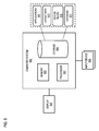
- FIG. 3A illustrates a design structure 300 a that may be used to determine the respective total capacitances of the plurality of integrated circuits.
- the design structure 300 a includes a pad 301 a that is electrically connected to n integrated circuits (e.g., integrated circuits 303 a , 303 b , . . . , 303 n ).
- n integrated circuits e.g., integrated circuits 303 a , 303 b , . . . , 303 n .
- each integrated circuit 303 a through 303 n contains identical arrays of bitcells except that the bitcells for different integrated circuits have different transistor channel widths.
- the pad 301 a is electrically connected through connections 305 to the gates of the transistors of integrated circuits 303 a through 303 n .
- the pad 301 a is further electrically connected through connections 307 to the shorted sources and drains of the transistors of the integrated circuits 303 a through 303 n .
- the pad 301 a is also electrically connected through connections 309 to the substrates of the integrated circuits 303 a through 303 n .
- the design structure 300 a allows for determining the total capacitance of respective integrated circuits between gate nodes and shorted source, drain and/or substrate nodes for n integrated circuits.
- each of the n integrated circuits may have identical transistors except for different channel widths between the integrated circuits.
- the design structure 300 a allows for determining respective total capacitances of the integrated circuits varying based on transistor channel widths.
- the gate dielectric layer of the transistors may vary between groups of integrated circuits.
- groups of integrated circuits may have transistors with identical transistor channel widths but with different gate dielectric layers.
- the gate dielectric layers may vary between thicknesses, types of oxides used, single or multiple different oxides used in the same gate oxide layer (e.g., multi-layers), and the like. Respective total capacitances may be determined for the integrated circuits with varying gate dielectric layers to further determine the effective channel width of the transistors, as discussed in more detail below.
- respective metal line capacitances of the plurality of integrated circuits are determined.
- the respective metal line capacitances are determined for the plurality of integrated circuits, with the integrated circuits lacking gate, source, and drain contacts for the transistors.
- the metal line capacitances may be determined by using modified (mirror) integrated circuits that lack the connections between the gate and source/drain nodes.
- the resulting respective metal line capacitances are the capacitances, therefore, resulting only from the metal lines within the integrated circuits.
- FIG. 3B illustrates a design structure 300 b that may be used to determine the respective metal line capacitances of the plurality of integrated circuits.
- the design structure 300 b includes a pad 301 b that is electrically connected to n integrated circuits (e.g., integrated circuits 311 a , 311 b , . . . , 311 n ).
- the integrated circuits 311 a , 311 b , . . . , 311 n may be the same integrated circuits as integrated circuits 303 a , 303 b , . . . , 303 n , but without the contacts to the gate, source, and drain nodes.
- the pad 301 b is electrically connected through connections 313 to the metal lines of the transistors of the integrated circuits 311 a through 311 n .
- the pad 301 b may additionally be electrically connected through connections 315 to the metal lines of the transistors of the integrated circuits 311 a through 311 n .
- the pad 301 b is also electrically connected through connections 309 to the substrates of the integrated circuits 311 a through 311 n .
- the design structure 300 b allows for determining the metal line capacitances of respective integrated circuits for n integrated circuits.
- each of the n integrated circuits may have identical transistors except for different channel widths between the integrated circuits.
- the design structure 300 b allows for determining metal line capacitances of the integrated circuits, without contacts to the gate, source, and drain nodes, varying based on transistor channel widths.
- the parallel line capacitance between the gate poly endcap and trench silicide lines is determined corresponding to the plurality of integrated circuits.
- the parallel line capacitance may be a generic capacitance determined and/or measured based on a generic structure, such as a scribe line test structure, that determines the capacitance between the gate poly endcap and the trench silicide lines corresponding to the integrated circuits.
- a generic structure such as a scribe line test structure
- the overlap capacitance between the gate node and the source node and/or the drain node corresponding to the plurality of integrated circuits is determined.
- the overlap capacitance also may be a generic capacitance measured from a generic structure, such as a scribe line test structure, that determines the capacitance between the gate node and the source node and/or the drain node corresponding to the integrated circuits.
- a generic structure such as a scribe line test structure
- the cap capacitance between the gate poly endcap and the substrate corresponding to the plurality of integrated circuits is determined.
- the cap capacitance may be determined based on the respective total capacitances described above with respect to step 201 versus the drawn transistor channel widths of the transistors of the plurality of integrated circuits.
- FIG. 4 illustrates a plot 400 of respective total capacitances C tot along the y-axis versus the drawn transistor channel widths of the transistors of the plurality of integrated circuits along the x-axis represented by data points 401 .
- the value of the drawn transistor channel width may be in nm, and the value of the respective total capacitances may be picofarads (pf).
- the data points 401 and values of the x and y-axes are merely exemplary and are not intended to illustrate actual values of respective total capacitances versus drawn transistor channel widths for integrated circuits.
- Trend line 403 is determined based on the trend of the data points 401 , with the y-intercept 405 of the trend line 403 based, at least in part, on the cap capacitance.
- C tot is the total capacitance of an integrated circuit
- W eff is the effective channel width of the transistors in the integrated circuit
- L is the length of the channel
- C m1 is respective metal line capacitance of the integrated circuit
- C ov is the overlap capacitance
- C cap is the cap capacitance
- C pcts is the parallel line capacitance corresponding to the integrated circuit.
- C gate is the capacitance from the gate, which may be determined based on the dielectric or permittivity (e.g., ⁇ ox ) of the gate dielectric (e.g., silicon dioxide) divided by the inversion layer thickness, which may be measured from a generic large area using a generic test structure, such as a scribe line test structure.
- the effective channel width W eff is zero, i.e., the y-intercept 405 of the trend line 403
- Equation 1 may be solved for the effective channel width W eff , resulting in:
- the effective channel width may be determined for the transistors in each of the integrated circuits used to determine the respective total capacitances. Further, knowing the drawn channel width for the transistors that resulted in manufactured transistors with the resulting total capacitances C tot allows for relating the drawn channel width to the effective channel width of the resulting transistor. This relationship may then be used for determining a target channel width for a target transistor based on the effective channel widths for precisely and accurately manufacturing devices while obtaining performance and functional yield targets.
- I gate is the dielectric tunneling current
- I gpa is the gate current per unit area, which can be considered constant for a given wafer for an integrated circuit
- L is the length of the transistor channel
- W actual is the effective channel width. Because the gate current per unit area I gpa is constant and the length L is known, L ⁇ I gpa equates to the slope of the best fit line for the gate current I gate versus drawn width of the transistor channel.
- the dielectric tunneling current I gpa may then be determined for a plurality of integrated circuits with uniform conditions except for different channel widths to determine the slope.
- the effective channel width may be determined without constructing and/or modifying the integrated circuits to not include contacts for the gate, source and drain, and there is no dependence on other standard structures, such as the generic structures discussed above. Rather, the integrated circuits may be measured directly for the dielectric tunneling current.
- the length of the transistor channel may be determined based on manipulating Equations 4 and 5 to provide for the slope of the gate current versus drawn transistor channel width per gate current per unit area.
- Computer system 500 includes at least one processor 501 , at least one memory 503 , and at least one storage 505 .
- Computer system 500 may be coupled to display 507 and one or more input devices 509 , such as a keyboard and a pointing device.
- Display 507 may be utilized to provide one or more GUI interfaces.
- Input devices 509 may be utilized by users of computer system 500 to interact with, for instance, the GUI interfaces.
- Storage 505 may store applications 511 , layout data (or information) 513 , design plus rules 515 , and at least one shape database (or repository) 517 .
- Applications 511 may include instructions (or computer program code) that when executed by processor 501 cause computer system 500 to perform one or more processes, such as one or more of the processes described herein.
- applications 511 may include one or more manufacturability analysis and/or yield enhancement tools.
- the embodiments of the present disclosure achieve several technical effects, including determining metal-oxide-semiconductor field-effect transistor (MOSFET) device channel widths, particularly for 20 nm technology nodes and beyond.
- MOSFET metal-oxide-semiconductor field-effect transistor
- the present disclosure enjoys industrial applicability associated with the designing and manufacturing of any of various types of highly integrated semiconductor devices used in microprocessors, smart phones, mobile phones, cellular handsets, set-top boxes, DVD recorders and players, automotive navigation, printers and peripherals, networking and telecom equipment, gaming systems, and digital cameras.
Landscapes
- Engineering & Computer Science (AREA)
- Computer Hardware Design (AREA)
- Physics & Mathematics (AREA)
- Theoretical Computer Science (AREA)
- General Physics & Mathematics (AREA)
- Evolutionary Computation (AREA)
- Geometry (AREA)
- General Engineering & Computer Science (AREA)
- Design And Manufacture Of Integrated Circuits (AREA)
Abstract
Description
C tot =W eff LC gate +W eff C ov+2LC cap +C m1 +C pcts (1)
where Ctot is the total capacitance of an integrated circuit, Weff is the effective channel width of the transistors in the integrated circuit, L is the length of the channel, Cm1 is respective metal line capacitance of the integrated circuit, and Cov is the overlap capacitance, Ccap is the cap capacitance, and Cpcts is the parallel line capacitance corresponding to the integrated circuit. Further, Cgate is the capacitance from the gate, which may be determined based on the dielectric or permittivity (e.g., ∈ox) of the gate dielectric (e.g., silicon dioxide) divided by the inversion layer thickness, which may be measured from a generic large area using a generic test structure, such as a scribe line test structure. When the effective channel width Weff is zero, i.e., the y-
C tot=2LC cap +C m1 +C pcts (2)
such that the cap capacitance Ccap can be determined based on the respective metal line capacitance Cm1, the cap capacitance Ccap, and the length L.
Thus, at
I gate =W actual ×L×I gpa (4)
where Igate is the dielectric tunneling current, Igpa is the gate current per unit area, which can be considered constant for a given wafer for an integrated circuit, L is the length of the transistor channel, and Wactual is the effective channel width. Because the gate current per unit area Igpa is constant and the length L is known, L×Igpa equates to the slope of the best fit line for the gate current Igate versus drawn width of the transistor channel. The dielectric tunneling current Igpa may then be determined for a plurality of integrated circuits with uniform conditions except for different channel widths to determine the slope. The effective channel width Wactual can then be determined based on:
W actual =I gate/slope (5)
Based on this approach, the effective channel width may be determined without constructing and/or modifying the integrated circuits to not include contacts for the gate, source and drain, and there is no dependence on other standard structures, such as the generic structures discussed above. Rather, the integrated circuits may be measured directly for the dielectric tunneling current. Moreover, the length of the transistor channel may be determined based on manipulating
Claims (18)
Priority Applications (1)
| Application Number | Priority Date | Filing Date | Title |
|---|---|---|---|
| US14/054,040 US9564375B2 (en) | 2013-10-15 | 2013-10-15 | Structures and methods for extraction of device channel width |
Applications Claiming Priority (1)
| Application Number | Priority Date | Filing Date | Title |
|---|---|---|---|
| US14/054,040 US9564375B2 (en) | 2013-10-15 | 2013-10-15 | Structures and methods for extraction of device channel width |
Publications (2)
| Publication Number | Publication Date |
|---|---|
| US20150102826A1 US20150102826A1 (en) | 2015-04-16 |
| US9564375B2 true US9564375B2 (en) | 2017-02-07 |
Family
ID=52809160
Family Applications (1)
| Application Number | Title | Priority Date | Filing Date |
|---|---|---|---|
| US14/054,040 Expired - Fee Related US9564375B2 (en) | 2013-10-15 | 2013-10-15 | Structures and methods for extraction of device channel width |
Country Status (1)
| Country | Link |
|---|---|
| US (1) | US9564375B2 (en) |
Citations (20)
| Publication number | Priority date | Publication date | Assignee | Title |
|---|---|---|---|---|
| US5446676A (en) * | 1993-03-29 | 1995-08-29 | Epic Design Technology Inc. | Transistor-level timing and power simulator and power analyzer |
| US5773317A (en) * | 1995-12-15 | 1998-06-30 | Vlsi Technology Inc. | Test structure and method for determining metal-oxide-silicon field effect transistor fringing capacitance |
| US6246973B1 (en) * | 1998-08-14 | 2001-06-12 | Motorola, Inc. | Modeling method of MOSFET |
| US20020167034A1 (en) * | 2001-05-09 | 2002-11-14 | Mitsubishi Denki Kabushiki Kaisha | Semiconductor device evaluation method and apparatus, semiconductor device manufacturing control method, semiconductor device manufacturing method, and recording medium |
| US20020188913A1 (en) * | 2001-06-12 | 2002-12-12 | Mitsubishi Denki Kabushiki Kaisha | Apparatus and method of layout generation, and program thereof |
| US6727724B2 (en) * | 1998-08-25 | 2004-04-27 | Renesas Technology Corp. | Characteristic evaluation apparatus for insulated gate type transistors |
| US20050027501A1 (en) * | 2003-06-09 | 2005-02-03 | Cadence Design Systems, Inc. | Method and apparatus for modeling devices having different geometries |
| US20080062596A1 (en) * | 2006-08-31 | 2008-03-13 | Freescale Semiconductor, Inc. | Distributed electrostatic discharge protection circuit with varying clamp size |
| US20080177523A1 (en) * | 2007-01-19 | 2008-07-24 | Advanced Micro Devices, Inc. | Method for quality assured semiconductor device modeling |
| US7514940B1 (en) * | 2006-12-13 | 2009-04-07 | National Semiconductor Corporation | System and method for determining effective channel dimensions of metal oxide semiconductor devices |
| US7730432B1 (en) * | 2005-03-30 | 2010-06-01 | Tela Innovations, Inc. | Method and system for reshaping a transistor gate in an integrated circuit to achieve a target objective |
| US20110022997A1 (en) * | 2009-07-27 | 2011-01-27 | Kuo-Liang Yeh | Method for conjecturing effective width and effective length of gate |
| US20120011479A1 (en) * | 2009-01-27 | 2012-01-12 | Synopsys, Inc. | Boosting transistor performance with non-rectangular channels |
| US20120117519A1 (en) * | 2010-11-03 | 2012-05-10 | Texas Instruments Incorporated | Method of transistor matching |
| US20130042216A1 (en) * | 2011-08-12 | 2013-02-14 | William Loh | Row Based Analog Standard Cell Layout Design and Methodology |
| US20130239077A1 (en) * | 2012-03-08 | 2013-09-12 | Taiwan Semiconductor Manufacturing Company, Ltd. | LVS Implementation for FinFET Design |
| US20140201700A1 (en) * | 2013-01-15 | 2014-07-17 | International Business Machines Corporation | Apparatus for modeling of finfet width quantization |
| US8972917B1 (en) * | 2013-09-26 | 2015-03-03 | International Business Machines Corporation | System and method for generating a field effect transistor corner model |
| US20150187655A1 (en) * | 2013-12-31 | 2015-07-02 | Texas Instruments Incorporated | Method to improve transistor matching |
| US20150279831A1 (en) * | 2014-03-25 | 2015-10-01 | International Business Machines Corporation | Determining threshold voltage variations in field effect transistors |
-
2013
- 2013-10-15 US US14/054,040 patent/US9564375B2/en not_active Expired - Fee Related
Patent Citations (25)
| Publication number | Priority date | Publication date | Assignee | Title |
|---|---|---|---|---|
| US5446676A (en) * | 1993-03-29 | 1995-08-29 | Epic Design Technology Inc. | Transistor-level timing and power simulator and power analyzer |
| US5773317A (en) * | 1995-12-15 | 1998-06-30 | Vlsi Technology Inc. | Test structure and method for determining metal-oxide-silicon field effect transistor fringing capacitance |
| US6246973B1 (en) * | 1998-08-14 | 2001-06-12 | Motorola, Inc. | Modeling method of MOSFET |
| US6727724B2 (en) * | 1998-08-25 | 2004-04-27 | Renesas Technology Corp. | Characteristic evaluation apparatus for insulated gate type transistors |
| US20020167034A1 (en) * | 2001-05-09 | 2002-11-14 | Mitsubishi Denki Kabushiki Kaisha | Semiconductor device evaluation method and apparatus, semiconductor device manufacturing control method, semiconductor device manufacturing method, and recording medium |
| US20020188913A1 (en) * | 2001-06-12 | 2002-12-12 | Mitsubishi Denki Kabushiki Kaisha | Apparatus and method of layout generation, and program thereof |
| US6584599B2 (en) * | 2001-06-12 | 2003-06-24 | Mitsubishi Denki Kabushiki Kaisha | Apparatus and method of layout generation, and program thereof |
| US20050027501A1 (en) * | 2003-06-09 | 2005-02-03 | Cadence Design Systems, Inc. | Method and apparatus for modeling devices having different geometries |
| US7730432B1 (en) * | 2005-03-30 | 2010-06-01 | Tela Innovations, Inc. | Method and system for reshaping a transistor gate in an integrated circuit to achieve a target objective |
| US20080062596A1 (en) * | 2006-08-31 | 2008-03-13 | Freescale Semiconductor, Inc. | Distributed electrostatic discharge protection circuit with varying clamp size |
| US7514940B1 (en) * | 2006-12-13 | 2009-04-07 | National Semiconductor Corporation | System and method for determining effective channel dimensions of metal oxide semiconductor devices |
| US7844927B2 (en) * | 2007-01-19 | 2010-11-30 | Globalfoundries Inc. | Method for quality assured semiconductor device modeling |
| US20080177523A1 (en) * | 2007-01-19 | 2008-07-24 | Advanced Micro Devices, Inc. | Method for quality assured semiconductor device modeling |
| US20120011479A1 (en) * | 2009-01-27 | 2012-01-12 | Synopsys, Inc. | Boosting transistor performance with non-rectangular channels |
| US20110022997A1 (en) * | 2009-07-27 | 2011-01-27 | Kuo-Liang Yeh | Method for conjecturing effective width and effective length of gate |
| US20120117519A1 (en) * | 2010-11-03 | 2012-05-10 | Texas Instruments Incorporated | Method of transistor matching |
| US20130042216A1 (en) * | 2011-08-12 | 2013-02-14 | William Loh | Row Based Analog Standard Cell Layout Design and Methodology |
| US20130239077A1 (en) * | 2012-03-08 | 2013-09-12 | Taiwan Semiconductor Manufacturing Company, Ltd. | LVS Implementation for FinFET Design |
| US20140201700A1 (en) * | 2013-01-15 | 2014-07-17 | International Business Machines Corporation | Apparatus for modeling of finfet width quantization |
| US8806419B2 (en) * | 2013-01-15 | 2014-08-12 | International Business Machines Corporation | Apparatus for modeling of FinFET width quantization |
| US8972917B1 (en) * | 2013-09-26 | 2015-03-03 | International Business Machines Corporation | System and method for generating a field effect transistor corner model |
| US20150089464A1 (en) * | 2013-09-26 | 2015-03-26 | International Business Machines Corporation | System and method for generating a field effect transistor corner model |
| US20150187655A1 (en) * | 2013-12-31 | 2015-07-02 | Texas Instruments Incorporated | Method to improve transistor matching |
| US20150279831A1 (en) * | 2014-03-25 | 2015-10-01 | International Business Machines Corporation | Determining threshold voltage variations in field effect transistors |
| US9209167B2 (en) * | 2014-03-25 | 2015-12-08 | International Business Machines Corporation | Determining threshold voltage variations in field effect transistors |
Also Published As
| Publication number | Publication date |
|---|---|
| US20150102826A1 (en) | 2015-04-16 |
Similar Documents
| Publication | Publication Date | Title |
|---|---|---|
| US8691599B2 (en) | Parameter extraction method for semiconductor device | |
| US8664968B2 (en) | On-die parametric test modules for in-line monitoring of context dependent effects | |
| US11378611B1 (en) | Measurement method for contact resistance of transistor test device and computer-readable medium | |
| US20130173214A1 (en) | Method and structure for inline electrical fin critical dimension measurement | |
| US12313679B2 (en) | Leakage testing structure and leakage testing method | |
| CN106599336B (en) | Semiconductor process simulation device and method and computing device | |
| CN107622959B (en) | Calibration method for MOS capacitor CV characteristic curve in TCAD simulation | |
| US7761823B2 (en) | Method for adjusting a transistor model for increased circuit simulation accuracy | |
| US10852337B2 (en) | Test structures for measuring silicon thickness in fully depleted silicon-on-insulator technologies | |
| US9564375B2 (en) | Structures and methods for extraction of device channel width | |
| US8832619B2 (en) | Analytical model for predicting current mismatch in metal oxide semiconductor arrays | |
| CN114446378B (en) | Parasitic capacitance detection method, memory and readable storage medium | |
| Niemeier et al. | Modeling off-state harmonics in MOS transistors used as RF switches | |
| US9916413B2 (en) | Transistor plasma charging metal design rule generator | |
| CN104103628A (en) | Test structure for transistor overlap capacitance and test method thereof | |
| Ma et al. | Non-logic devices in logic processes | |
| US20050260776A1 (en) | Structure and method for extraction of parasitic junction capacitance in deep submicron technology | |
| CN100362358C (en) | Scattering Measurement Method of Ring Oscillator | |
| US10529631B1 (en) | Test structures and method for electrical measurement of FinFET fin height | |
| CN112331579B (en) | Test structure and test methods | |
| US7504270B2 (en) | Methods of quantifying variations resulting from manufacturing-induced corner rounding of various features, and structures for testing same | |
| Cong et al. | A design TCADAS tool for semiconductor devices and case study of 65 nm conventional floating-gate MOS transistor | |
| JP2003023078A (en) | Method and apparatus for evaluating integrated circuit design and program | |
| US9029172B2 (en) | On-chip poly-to-contact process monitoring and reliability evaluation system and method of use | |
| US20160126194A1 (en) | Measurement mark structure and manufacturing method thereof |
Legal Events
| Date | Code | Title | Description |
|---|---|---|---|
| AS | Assignment |
Owner name: GLOBALFOUNDRIES INC., CAYMAN ISLANDS Free format text: ASSIGNMENT OF ASSIGNORS INTEREST;ASSIGNORS:MANN, RANDY;WU, XUSHENG;GHOSH, SONIA;AND OTHERS;SIGNING DATES FROM 20130917 TO 20130918;REEL/FRAME:031407/0353 |
|
| STCF | Information on status: patent grant |
Free format text: PATENTED CASE |
|
| CC | Certificate of correction | ||
| AS | Assignment |
Owner name: WILMINGTON TRUST, NATIONAL ASSOCIATION, DELAWARE Free format text: SECURITY AGREEMENT;ASSIGNOR:GLOBALFOUNDRIES INC.;REEL/FRAME:049490/0001 Effective date: 20181127 |
|
| FEPP | Fee payment procedure |
Free format text: MAINTENANCE FEE REMINDER MAILED (ORIGINAL EVENT CODE: REM.); ENTITY STATUS OF PATENT OWNER: LARGE ENTITY |
|
| AS | Assignment |
Owner name: GLOBALFOUNDRIES INC., CAYMAN ISLANDS Free format text: RELEASE BY SECURED PARTY;ASSIGNOR:WILMINGTON TRUST, NATIONAL ASSOCIATION;REEL/FRAME:054636/0001 Effective date: 20201117 |
|
| LAPS | Lapse for failure to pay maintenance fees |
Free format text: PATENT EXPIRED FOR FAILURE TO PAY MAINTENANCE FEES (ORIGINAL EVENT CODE: EXP.); ENTITY STATUS OF PATENT OWNER: LARGE ENTITY |
|
| STCH | Information on status: patent discontinuation |
Free format text: PATENT EXPIRED DUE TO NONPAYMENT OF MAINTENANCE FEES UNDER 37 CFR 1.362 |
|
| FP | Lapsed due to failure to pay maintenance fee |
Effective date: 20210207 |
|
| AS | Assignment |
Owner name: GLOBALFOUNDRIES U.S. INC., NEW YORK Free format text: RELEASE BY SECURED PARTY;ASSIGNOR:WILMINGTON TRUST, NATIONAL ASSOCIATION;REEL/FRAME:056987/0001 Effective date: 20201117 Owner name: GLOBALFOUNDRIES U.S. INC., NEW YORK Free format text: RELEASE OF SECURITY INTEREST;ASSIGNOR:WILMINGTON TRUST, NATIONAL ASSOCIATION;REEL/FRAME:056987/0001 Effective date: 20201117 |