US9563584B2 - Method and device for buffer processing in system on chip - Google Patents
Method and device for buffer processing in system on chip Download PDFInfo
- Publication number
- US9563584B2 US9563584B2 US14/442,066 US201314442066A US9563584B2 US 9563584 B2 US9563584 B2 US 9563584B2 US 201314442066 A US201314442066 A US 201314442066A US 9563584 B2 US9563584 B2 US 9563584B2
- Authority
- US
- United States
- Prior art keywords
- datum
- buffer space
- start address
- valid
- read
- Prior art date
- Legal status (The legal status is an assumption and is not a legal conclusion. Google has not performed a legal analysis and makes no representation as to the accuracy of the status listed.)
- Active
Links
- 239000000872 buffer Substances 0.000 title claims abstract description 216
- 238000000034 method Methods 0.000 title claims abstract description 59
- 230000008569 process Effects 0.000 claims description 15
- 239000012634 fragment Substances 0.000 description 18
- 230000009286 beneficial effect Effects 0.000 description 3
- 230000003139 buffering effect Effects 0.000 description 3
- 238000010586 diagram Methods 0.000 description 2
- 238000007726 management method Methods 0.000 description 2
- 239000013589 supplement Substances 0.000 description 2
- 230000008859 change Effects 0.000 description 1
- 230000003993 interaction Effects 0.000 description 1
- 230000002093 peripheral effect Effects 0.000 description 1
- 230000003068 static effect Effects 0.000 description 1
Images


Classifications
-
- G—PHYSICS
- G06—COMPUTING; CALCULATING OR COUNTING
- G06F—ELECTRIC DIGITAL DATA PROCESSING
- G06F13/00—Interconnection of, or transfer of information or other signals between, memories, input/output devices or central processing units
- G06F13/14—Handling requests for interconnection or transfer
- G06F13/16—Handling requests for interconnection or transfer for access to memory bus
- G06F13/1668—Details of memory controller
- G06F13/1673—Details of memory controller using buffers
-
- G—PHYSICS
- G06—COMPUTING; CALCULATING OR COUNTING
- G06F—ELECTRIC DIGITAL DATA PROCESSING
- G06F12/00—Accessing, addressing or allocating within memory systems or architectures
- G06F12/02—Addressing or allocation; Relocation
- G06F12/0223—User address space allocation, e.g. contiguous or non contiguous base addressing
- G06F12/023—Free address space management
-
- G—PHYSICS
- G06—COMPUTING; CALCULATING OR COUNTING
- G06F—ELECTRIC DIGITAL DATA PROCESSING
- G06F12/00—Accessing, addressing or allocating within memory systems or architectures
- G06F12/02—Addressing or allocation; Relocation
- G06F12/08—Addressing or allocation; Relocation in hierarchically structured memory systems, e.g. virtual memory systems
-
- G—PHYSICS
- G06—COMPUTING; CALCULATING OR COUNTING
- G06F—ELECTRIC DIGITAL DATA PROCESSING
- G06F9/00—Arrangements for program control, e.g. control units
- G06F9/06—Arrangements for program control, e.g. control units using stored programs, i.e. using an internal store of processing equipment to receive or retain programs
- G06F9/46—Multiprogramming arrangements
- G06F9/468—Specific access rights for resources, e.g. using capability register
-
- G—PHYSICS
- G06—COMPUTING; CALCULATING OR COUNTING
- G06F—ELECTRIC DIGITAL DATA PROCESSING
- G06F9/00—Arrangements for program control, e.g. control units
- G06F9/06—Arrangements for program control, e.g. control units using stored programs, i.e. using an internal store of processing equipment to receive or retain programs
- G06F9/46—Multiprogramming arrangements
- G06F9/50—Allocation of resources, e.g. of the central processing unit [CPU]
-
- G—PHYSICS
- G11—INFORMATION STORAGE
- G11C—STATIC STORES
- G11C8/00—Arrangements for selecting an address in a digital store
- G11C8/06—Address interface arrangements, e.g. address buffers
-
- G—PHYSICS
- G06—COMPUTING; CALCULATING OR COUNTING
- G06F—ELECTRIC DIGITAL DATA PROCESSING
- G06F2212/00—Indexing scheme relating to accessing, addressing or allocation within memory systems or architectures
- G06F2212/10—Providing a specific technical effect
- G06F2212/1041—Resource optimization
- G06F2212/1044—Space efficiency improvement
Definitions
- the disclosure relates to the field of network storage, and in particular to a method and device for buffer processing in a System on Chip SOC).
- a SoC technology integrates a Central Processing Unit/Micro Process Unit (CPU/PU), a Digital Signal Processor (DSP), a hardware accelerator, a memory, a peripheral interface and other subsystems into a chip through bus interconnection.
- CPU/PU Central Processing Unit/Micro Process Unit
- DSP Digital Signal Processor
- These centralized buffers shared by multiple sources/multiple users can be one or several storage units physically, such as a Static Random-Access Memory (SRAM), or a Dynamic Random-Access Memory (DRAM), or several combinations of them, but they can be regarded as a shared buffer logically.
- SRAM Static Random-Access Memory
- DRAM Dynamic Random-Access Memory
- the shared buffer described below is discussed on a basis that it is logically a storage unit, but actually it physically can be a storage unit or a combination of several storage units.
- a method of using a shared buffer in a SoC design is basically dividing the shared buffer into N fragments with the same size; the size of such a fragment is required to be capable of holding the minimum data needed by each source/each user; big data occupies M fragments, wherein M is an integer, and M is less than or equal to N.
- This method is disadvantaged in needing a very large storage space to record a use state and storage location information of each fragment. Especially, when the length of the minimum data needed by a system is very short, the space for storage of each fragment is also very small; when big data is stored, many fragments are needed. In addition, this method wastes a shared buffer space, for example, some data are only a little bit bigger than an integral number of fragments, and need to be stored in another single fragment.
- a technical problem to he solved by the disclosure is to provide a method and device for buffer processing in a SoC which can realize better planning and management and economize a buffer space.
- an embodiment of the disclosure provides a method for buffer processing in a SoC, which includes that:
- the first datum is stored into a buffer space from the current storage start address, wherein the buffer space occupied by the first datum is a first buffer space;
- storage location information including a start address and a space length of the first buffer space is saved, so as to locate the first buffer space according to the start address and the space length when the first datum needs to be read, and to read the first datum from the first buffer space; and the current storage start address is updated with a next address of the first buffer space, so as to buffer next data needed to be buffered from the updated current storage start address.
- the method further may include that:
- an idle state of the first datum is recorded, and it is determined that whether the first datum is released according to the idle state.
- the method may further include that:
- a threshold value is set, wherein the threshold value is a buffer space size needed for storing a maximum datum
- the predetermined method is selecting from the buffer space an invalid datum stored at the earliest, and consecutively storing, from a start address of the selected invalid datum, valid data behind the selected invalid datum until all the valid data consecutively occupy the buffer space; wherein the invalid datum is a released datum, and the valid data are data not released;
- the current storage start address is updated with a next address of a last valid datum in the buffer space.
- the predetermined method may be that:
- the invalid datum stored at the earliest is selected from the buffer space, a start address of the selected invalid datum in the buffer space is obtained through storage location information of the selected invalid datum, and the current storage start address is updated with the start address of the selected invalid datum;
- a first valid datum behind the selected invalid datum is stored from the updated current storage start address, and storage location information of the first valid datum is updated;
- the current storage start address is updated with a next address of the first valid datum in the buffer space, so as to buffer a next valid data behind the first valid datum from the updated current storage start address until each buffered valid datum is capable of consecutively occupying the buffer space.
- the method may further include that:
- the disclosure also provides a device for buffer processing in a SoC, including a processor configured to be capable of executing programmed instructions comprising:
- the buffer space occupied by the first datum is a first buffer space
- the first datum saving storage location information comprising a start address and a space length of the first buffer space, to locate the first buffer space according to the start address and the space length of the first buffer space when the first datum needs to be read and reading the first datum from the first buffer space;
- the processor configured to be capable of executing programmed instructions further comprising: recording an idle state of the first datum, and determine whether the first datum is released according to the idle state,
- the processor configured to be capable of executing programmed instructions further comprising;
- threshold value is a buffer space size needed for storing a maximum datum
- the predefined method is selecting from the buffer space an invalid datum stored at the earliest, and consecutively storing, from a start address of the selected invalid datum, valid data behind the selected invalid datum until all the valid data consecutively occupy the buffer space; wherein the invalid datum is a released datum, and The valid data are data not released;
- the processor configured to be capable of executing programmed instructions further comprising:
- consecutively storing data in a buffer space can make better use of the buffer space; furthermore, in the prior art, it is needed to record buffer addresses of these fragments for reading data, so the amount of stored information is very large, while in the embodiments of the disclosure, data are consecutively stored into the buffer space, so data can be read as long as the start address of each datum in the buffer space and the space length are recorded, and the amount of stored information depends on the amount of packets.
- FIG. 1 is a diagram of a method for buffer processing according to embodiment 1 of the disclosure:
- FIG. 2 is a flowchart of a specific method for buffer processing according to embodiment 1 of the disclosure
- FIG. 3 is a flowchart of arranging a buffer space in the method for buffer processing according to embodiment 1 of the disclosure.
- FIG. 4 is a diagram of a device for buffer processing according to embodiment 2 of the disclosure.
- a method for buffer processing includes the following steps:
- Step 1 when a first datum of a first user needs to be buffered, a current storage start address is read;
- Step 2 the first datum is stored into a buffer space from the current storage start address, wherein the buffer space occupied by the first datum is a first buffer space;
- Step 3 corresponding to the first datum of the first user, storage location information including a start address and a space length of the first buffer space is saved, so that when the first datum needs to be read, the first buffer space can be located according to the start address and the space length, and the first datum can be read from the first buffer space; and
- Step 4 the current storage start address is updated with a next address of the first buffer space, so that a next datum needing to be buffered can be buffered from the storage start address, thus each buffered datum can consecutively occupy the buffer space.
- the method of the present embodiment consecutively stores data into a buffer space, which can make better use of the buffer space; furthermore, in the prior art, it is needed to record buffer addresses of these fragments for reading data, so the amount of stored information is very large, however, in the present embodiment data are consecutively stored into the buffer space, so data can be read as long as the start address of each datum in the buffer space and the space length are recorded, and the amount of stored information depends on the amount of packets.
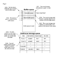
- Step S 201 the current storage start address st_add. 1 is read;
- Step S 202 the first datum of the first user is stored into the buffer space from the current storage start address st_add. 1 ; the buffer space occupied by the first datum is the first buffer space;
- Step S 203 for enabling each stored datum to consecutively occupy the buffer space, after Step S 203 is completed, Step 204 is performed, that is, the current storage start address is updated with the next address of the first buffer space;
- the storage start address should be st_add. 2 ; when it is needed to continue storing data, for example, a second datum, the following steps may be performed:
- Step S 205 the second datum is stored into the buffer space from the st_add. 2 , and the buffer space occupied by the second datum is a second buffer space (shown in FIG. 2 );
- the second datum is not necessarily the datum of the first user needing to be buffered, which may belong to other users;
- Step S 206 the start address (e.g., “st_add. 2 ” shown in FIG. 2 ) and the space length (e.g., “len. 2 ” shown in FIG. 2 ) of the second buffer space, and an idle state (e.g., “V” shown in FIG. 2 ) of the second datum are saved in the additional storage space; and
- Step S 207 the current storage start address is updated with a next address of the second buffer space.
- the method includes that:
- a threshold value is set, wherein the threshold value is a buffer space size which may be needed for storing a maximum datum;
- a remaining buffer space behind the current storage start address is smaller than the preset threshold value
- data in the buffer space are arranged by a predetermined method, and the start address of each datum is updated after the arrangement; wherein the predetermined method is selecting an invalid datum stored at the earliest from the buffer space, and consecutively storing, at the start address of the selected invalid datum, valid data behind the selected invalid datum until all the valid data consecutively occupy the buffer space; wherein the invalid datum is the released datum; the valid data is the data not released.
- the predetermined method is elaborated below.
- a threshold value is preset, wherein the threshold value is a space size needed for storing a maximum datum; if the remaining buffer space is smaller than the preset threshold value, then it is indicated that the buffer space not used currently cannot store the data 7 , and it is needed to arrange the buffer space, which includes the following steps:
- Step S 1 the current storage start address is updated with the start address of the data 2 ; the datum 3 is stored from the start address of the datum 2 (namely moving up the buffer space corresponding to the datum 3 for a distance, wherein the distance is equal to the space length of the datum 2 ), and the start address of the datum 2 recorded in the additional storage space is updated;
- Step S 2 the current storage start address is updated with the next address of the buffer space where the datum 3 is; the datum 4 is stored at the storage start address, and the start address of the datum 4 in the additional storage space is updated;
- Step S 3 the current storage start address is updated with the next address of the buffer space where the datum 4 is; the datum 6 is stored at the storage start address, so that the buffer space corresponding to the data 2 and 5 is integrated into the remaining buffer space behind the current storage start address; and then the start address of the datum 6 in the additional storage space is updated; and
- Step S 4 after arrangement of the buffer space is completed, the datum 7 is stored. Note that, all the valid data should consecutively occupy the buffer space.
- the target data being arranged may be read mistakenly due to the change of its location in the buffer space.
- a valid datum which is being read or arranged may be locked, so that the valid datum cannot be read and arranged simultaneously in the locking process.
- the datum 3 when the datum 3 is being arranged, it can be locked, and it will not unlocked until arrangement is completed; when the datum 3 is being locked, a reading request cannot be received, thereby preventing an arrangement process from disturbing a reading process.
- the whole buffer space is divided into a number of fragments, some big data are saved by many fragments, and it is needed to record buffer addresses of these fragments for reading data, so the amount of stored information is very large, while in the present embodiment, the buffer space consecutively stores the data, so reading can be implemented by only recoding the start address of each valid datum in the buffer space and the space length.
- a device for buffer processing includes:
- a storage start address reading module 41 which is configured to read the current storage start address when the first datum of the first user needs to be buffered;
- a buffering module 42 which is configured to store the first datum into the buffer space from the current storage start address, wherein the buffer space occupied by the first datum is the first buffer space;
- a storage data managing module 43 which is configured to, corresponding to the first datum of the first user, save the storage location information including the start address and the space length of the first buffer space, so that when the first datum needs to be read, the first buffer space can be located according to the start address and the space length, and the first datum can be read from the first buffer space;
- a storage start address updating module 44 which is configured to update the current storage start address with the next address of the first buffer space, so that a next datum needing to be buffered can be buffered from the storage start address, thus each buffered datum can consecutively occupy the buffer space.
- the storage data managing module 43 can also record the idle state of the first datum, and determine whether the first datum is released according to the idle state.
- the remaining buffer space behind the storage start address may be not enough for subsequent storage, while some buffered data have been read and released, and the buffer space corresponding to them has been cleared up, then it is needed to arrange the whole buffer space.
- the device may further include an arrangement module; wherein,
- the arrangement module will set a threshold value, and the threshold value is a buffer space size which may be needed for storing a maximum datum; if the remaining buffer space behind the current storage start address is smaller than the preset threshold value, the data in the buffer space are arranged by the predetermined method, and the start address of each datum is updated after the arrangement; wherein the predetermined method is selecting an invalid datum stored at the earliest from the buffer space, and consecutively storing, at the start address of the selected invalid datum, the valid data after the datum stored at the earliest until all the valid data consecutively occupy the buffer space; wherein the invalid datum is the released datum, and the valid data is the data not released.
- the storage start address updating module 44 updates the current storage start address with the next address of the last valid datum in the buffer space.
- the predetermined method is specifically selecting an invalid datum stored at the earliest from the buffer space, obtaining, through the storage location information of the selected invalid datum, the start address of the selected invalid datum in the buffer space, and updating the current storage start address with the start address of the selected invalid datum; storing the first valid datum behind the invalid datum from the storage start address, and updating the storage location information of the first valid datum; and updating the current storage start address with the next address of the first valid datum in the buffer space, so that the next valid data behind the first valid datum can be buffered again from the storage start address, until each buffered valid datum can consecutively occupy the buffer space.
- the device may further include a locking module; the locking module can lock a valid datum which is being read or arranged, so that the valid datum cannot be read and arranged simultaneously in the locking process.
- the storage start address reading module, the buffering module, the storage data managing module, the storage start address updating module, the arrangement module and the locking module can be implemented by a CPU, a DSP or a Field-Programmable Gate Array (FPGA) in the device for buffer processing.
- FPGA Field-Programmable Gate Array
- the whole buffer space is divided into a number of fragments, some big data are saved by many fragments, and it is needed to record buffer addresses of these fragments for reading data, so the amount of stored information is very large, but in the present embodiment, the buffer space consecutively stores the data, so reading can be implemented by only recoding the start address of each valid datum in the buffer space and the space length.
Landscapes
- Engineering & Computer Science (AREA)
- Theoretical Computer Science (AREA)
- Physics & Mathematics (AREA)
- General Engineering & Computer Science (AREA)
- General Physics & Mathematics (AREA)
- Software Systems (AREA)
- Microelectronics & Electronic Packaging (AREA)
- Memory System Of A Hierarchy Structure (AREA)
- Information Transfer Systems (AREA)
- Computer And Data Communications (AREA)
Abstract
Description
Claims (10)
Applications Claiming Priority (4)
| Application Number | Priority Date | Filing Date | Title |
|---|---|---|---|
| CN201210478383 | 2012-11-22 | ||
| CN201210478383.4 | 2012-11-22 | ||
| CN201210478383.4A CN103838679B (en) | 2012-11-22 | 2012-11-22 | A kind of method for caching and processing and device |
| PCT/CN2013/082050 WO2013189413A2 (en) | 2012-11-22 | 2013-08-22 | Buffer processing method and device |
Publications (2)
| Publication Number | Publication Date |
|---|---|
| US20150317264A1 US20150317264A1 (en) | 2015-11-05 |
| US9563584B2 true US9563584B2 (en) | 2017-02-07 |
Family
ID=49769556
Family Applications (1)
| Application Number | Title | Priority Date | Filing Date |
|---|---|---|---|
| US14/442,066 Active US9563584B2 (en) | 2012-11-22 | 2013-08-22 | Method and device for buffer processing in system on chip |
Country Status (5)
| Country | Link |
|---|---|
| US (1) | US9563584B2 (en) |
| EP (1) | EP2911061B1 (en) |
| JP (1) | JP6059360B2 (en) |
| CN (1) | CN103838679B (en) |
| WO (1) | WO2013189413A2 (en) |
Families Citing this family (2)
| Publication number | Priority date | Publication date | Assignee | Title |
|---|---|---|---|---|
| CN105550124A (en) * | 2015-12-09 | 2016-05-04 | 四川长虹电器股份有限公司 | Information processing method and electronic device |
| CN111767234A (en) * | 2020-06-28 | 2020-10-13 | 歌尔科技有限公司 | Data storage method, device, electronic product and computer readable storage medium |
Citations (14)
| Publication number | Priority date | Publication date | Assignee | Title |
|---|---|---|---|---|
| EP0294499A1 (en) | 1987-06-09 | 1988-12-14 | International Business Machines Corporation | Control scheme for segmented buffers based on a shared reference count |
| US5610809A (en) * | 1994-01-11 | 1997-03-11 | Mitsubishi Denki Kabushiki Kaisha | Programmable controller and program capacity changing method thereof |
| US5652883A (en) * | 1992-06-15 | 1997-07-29 | Microsoft Corporation | Computer method and system for conservative-stack and generational heap garbage collection |
| US20030131012A1 (en) | 2000-10-27 | 2003-07-10 | Joakim Dahlstedt | System and method for regeneration of methods and garbage collection of unused methods |
| US20030196044A1 (en) | 2002-04-12 | 2003-10-16 | Alejandro Ramirez | Cache-line reuse-buffer |
| CN1677946A (en) | 2004-04-02 | 2005-10-05 | 华为技术有限公司 | Buffer distribution method and apparatus |
| CN1725728A (en) | 2004-07-22 | 2006-01-25 | 华为技术有限公司 | Buffer management method based on signaling protocol |
| US20060036829A1 (en) * | 2004-08-12 | 2006-02-16 | Via Technologies Inc. | Memory space allocation methods and IC products utilizing the same |
| JP2006161864A (en) | 2004-12-02 | 2006-06-22 | Calsonic Kansei Corp | Select assist device for automatic transmission |
| CN101122886A (en) | 2007-09-03 | 2008-02-13 | 杭州华三通信技术有限公司 | Method and device for dispensing cache room and cache controller |
| CN101196857A (en) | 2008-01-04 | 2008-06-11 | 太原理工大学 | Double-port access symmetrical dynamic memory interface |
| JP2008241186A (en) | 2007-03-28 | 2008-10-09 | Daicel Chem Ind Ltd | Igniter assembly |
| CN102197381A (en) | 2008-10-28 | 2011-09-21 | Nxp股份有限公司 | Data processing circuit with cache and interface for a detachable device |
| CN102646084A (en) | 2012-03-06 | 2012-08-22 | 上海纳轩电子科技有限公司 | Efficient network packet storage method implemented based on FPGA (field programmable gate array) |
Family Cites Families (2)
| Publication number | Priority date | Publication date | Assignee | Title |
|---|---|---|---|---|
| JPH06161864A (en) * | 1992-11-19 | 1994-06-10 | Toshiba Corp | Object storage managing method |
| JPH08241186A (en) * | 1995-03-07 | 1996-09-17 | Fujitsu Ltd | Unit and method for buffer memory management |
-
2012
- 2012-11-22 CN CN201210478383.4A patent/CN103838679B/en active Active
-
2013
- 2013-08-22 US US14/442,066 patent/US9563584B2/en active Active
- 2013-08-22 EP EP13806128.8A patent/EP2911061B1/en active Active
- 2013-08-22 JP JP2015543258A patent/JP6059360B2/en active Active
- 2013-08-22 WO PCT/CN2013/082050 patent/WO2013189413A2/en active Application Filing
Patent Citations (16)
| Publication number | Priority date | Publication date | Assignee | Title |
|---|---|---|---|---|
| EP0294499A1 (en) | 1987-06-09 | 1988-12-14 | International Business Machines Corporation | Control scheme for segmented buffers based on a shared reference count |
| US5652883A (en) * | 1992-06-15 | 1997-07-29 | Microsoft Corporation | Computer method and system for conservative-stack and generational heap garbage collection |
| US5610809A (en) * | 1994-01-11 | 1997-03-11 | Mitsubishi Denki Kabushiki Kaisha | Programmable controller and program capacity changing method thereof |
| US7650370B2 (en) * | 1999-10-28 | 2010-01-19 | Bea Systems, Inc. | System and method for regeneration of methods and garbage collection of unused methods |
| US20050256913A1 (en) | 1999-10-28 | 2005-11-17 | Bea Systems, Inc. | System and method for regeneration of methods and garbage collection of unused methods |
| US20030131012A1 (en) | 2000-10-27 | 2003-07-10 | Joakim Dahlstedt | System and method for regeneration of methods and garbage collection of unused methods |
| US20030196044A1 (en) | 2002-04-12 | 2003-10-16 | Alejandro Ramirez | Cache-line reuse-buffer |
| CN1677946A (en) | 2004-04-02 | 2005-10-05 | 华为技术有限公司 | Buffer distribution method and apparatus |
| CN1725728A (en) | 2004-07-22 | 2006-01-25 | 华为技术有限公司 | Buffer management method based on signaling protocol |
| US20060036829A1 (en) * | 2004-08-12 | 2006-02-16 | Via Technologies Inc. | Memory space allocation methods and IC products utilizing the same |
| JP2006161864A (en) | 2004-12-02 | 2006-06-22 | Calsonic Kansei Corp | Select assist device for automatic transmission |
| JP2008241186A (en) | 2007-03-28 | 2008-10-09 | Daicel Chem Ind Ltd | Igniter assembly |
| CN101122886A (en) | 2007-09-03 | 2008-02-13 | 杭州华三通信技术有限公司 | Method and device for dispensing cache room and cache controller |
| CN101196857A (en) | 2008-01-04 | 2008-06-11 | 太原理工大学 | Double-port access symmetrical dynamic memory interface |
| CN102197381A (en) | 2008-10-28 | 2011-09-21 | Nxp股份有限公司 | Data processing circuit with cache and interface for a detachable device |
| CN102646084A (en) | 2012-03-06 | 2012-08-22 | 上海纳轩电子科技有限公司 | Efficient network packet storage method implemented based on FPGA (field programmable gate array) |
Non-Patent Citations (3)
| Title |
|---|
| English Translation of the Written Opinion of the International Search Authority in international application No. PCT/CN2013/082050, mailed on Nov. 28, 2013. |
| International Search Report in international application No. PCT/CN2013/082050, mailed on Nov. 28, 2013. |
| Supplementary European Search Report in European application number: 13806128.8, mailed on Oct. 12, 2015. |
Also Published As
| Publication number | Publication date |
|---|---|
| JP6059360B2 (en) | 2017-01-11 |
| WO2013189413A3 (en) | 2014-02-13 |
| WO2013189413A2 (en) | 2013-12-27 |
| CN103838679A (en) | 2014-06-04 |
| EP2911061A4 (en) | 2015-11-11 |
| US20150317264A1 (en) | 2015-11-05 |
| CN103838679B (en) | 2017-08-04 |
| JP2016504665A (en) | 2016-02-12 |
| EP2911061B1 (en) | 2022-03-30 |
| EP2911061A2 (en) | 2015-08-26 |
Similar Documents
| Publication | Publication Date | Title |
|---|---|---|
| US9098462B1 (en) | Communications via shared memory | |
| US10860493B2 (en) | Method and apparatus for data storage system | |
| US8250310B2 (en) | Assigning data to NVRAM of shared access hybrid hard drives | |
| US9032162B1 (en) | Systems and methods for providing memory controllers with memory access request merging capabilities | |
| CN110226157A (en) | Dynamic memory for reducing row buffering conflict remaps | |
| EP2645259B1 (en) | Method, device and system for caching data in multi-node system | |
| CN106951488B (en) | Log recording method and device | |
| US20150213105A1 (en) | Data processing method, apparatus, and storage medium | |
| US9178839B2 (en) | Sharing buffer space in link aggregation configurations | |
| US9753660B2 (en) | System and method for implementing hierarchical distributed-linked lists for network devices | |
| US11210228B2 (en) | Method, device and computer program product for cache management | |
| US20130290649A1 (en) | Forward counter block | |
| JP2020115367A (en) | Localized data affinity system and hybrid method | |
| CN101763433B (en) | Data storage system and method | |
| CN102833331A (en) | Cloud storage system and metadata writing-in method and metadata reading method thereof | |
| US8615642B2 (en) | Automatic page promotion and demotion in multiple page size environments | |
| US20240314021A1 (en) | Method, apparatus, electronic device and storage medium for resource operation | |
| US9563584B2 (en) | Method and device for buffer processing in system on chip | |
| CN117473011A (en) | Data synchronization method, device and hybrid cache system | |
| CN102073539B (en) | Queue request processing method and device | |
| US20170017567A1 (en) | System And Method For Implementing Distributed-Linked Lists For Network Devices | |
| CN116662603B (en) | Time shaft control method and system based on kafka, electronic equipment and storage medium | |
| CN116263746B (en) | Memory partitioning of processing entities | |
| TWI501255B (en) | Data backup method for flash memory module and solid state drive | |
| CN117170863A (en) | Memory allocation method, device, equipment and storage medium |
Legal Events
| Date | Code | Title | Description |
|---|---|---|---|
| AS | Assignment |
Owner name: ZTE CORPORATION, CHINA Free format text: ASSIGNMENT OF ASSIGNORS INTEREST;ASSIGNOR:ZHANG, LINSHENG;REEL/FRAME:036104/0458 Effective date: 20150505 |
|
| AS | Assignment |
Owner name: ZTE MICROELECTRONICS TECHNOLOGY CO., LTD., CHINA Free format text: ASSIGNMENT OF 50% INTEREST;ASSIGNOR:ZTE CORPORATION;REEL/FRAME:037515/0039 Effective date: 20151221 |
|
| STCF | Information on status: patent grant |
Free format text: PATENTED CASE |
|
| AS | Assignment |
Owner name: SANECHIPS TECHNOLOGY CO., LTD., CHINA Free format text: CHANGE OF NAME;ASSIGNOR:ZTE MICROELECTRONICS TECHNOLOGY CO., LTD.;REEL/FRAME:042320/0285 Effective date: 20161111 |
|
| CC | Certificate of correction | ||
| MAFP | Maintenance fee payment |
Free format text: PAYMENT OF MAINTENANCE FEE, 4TH YEAR, LARGE ENTITY (ORIGINAL EVENT CODE: M1551); ENTITY STATUS OF PATENT OWNER: LARGE ENTITY Year of fee payment: 4 |
|
| AS | Assignment |
Owner name: SANECHIPS TECHNOLOGY CO., LTD., CHINA Free format text: ASSIGNMENT OF ASSIGNORS INTEREST;ASSIGNOR:ZTE CORPORATION;REEL/FRAME:062777/0001 Effective date: 20221213 |
|
| MAFP | Maintenance fee payment |
Free format text: PAYMENT OF MAINTENANCE FEE, 8TH YEAR, LARGE ENTITY (ORIGINAL EVENT CODE: M1552); ENTITY STATUS OF PATENT OWNER: LARGE ENTITY Year of fee payment: 8 |