US9563095B2 - Pixel structure and manufacturing method therefor, array structure, display panel and display device - Google Patents
Pixel structure and manufacturing method therefor, array structure, display panel and display device Download PDFInfo
- Publication number
- US9563095B2 US9563095B2 US14/742,599 US201514742599A US9563095B2 US 9563095 B2 US9563095 B2 US 9563095B2 US 201514742599 A US201514742599 A US 201514742599A US 9563095 B2 US9563095 B2 US 9563095B2
- Authority
- US
- United States
- Prior art keywords
- pixel
- tft
- pixel unit
- electrode
- electrically connected
- Prior art date
- Legal status (The legal status is an assumption and is not a legal conclusion. Google has not performed a legal analysis and makes no representation as to the accuracy of the status listed.)
- Active
Links
- 238000004519 manufacturing process Methods 0.000 title claims abstract description 14
- 239000000758 substrate Substances 0.000 claims description 30
- 239000011159 matrix material Substances 0.000 claims description 5
- 239000010408 film Substances 0.000 claims description 4
- 239000010409 thin film Substances 0.000 claims description 2
- 238000010586 diagram Methods 0.000 description 14
- 239000004973 liquid crystal related substance Substances 0.000 description 9
- 238000002834 transmittance Methods 0.000 description 5
- 230000005684 electric field Effects 0.000 description 4
- 238000012986 modification Methods 0.000 description 4
- 230000004048 modification Effects 0.000 description 4
- 238000005516 engineering process Methods 0.000 description 3
- 238000000034 method Methods 0.000 description 3
- 230000000694 effects Effects 0.000 description 2
- 238000007792 addition Methods 0.000 description 1
- 239000004020 conductor Substances 0.000 description 1
- 239000011521 glass Substances 0.000 description 1
- AMGQUBHHOARCQH-UHFFFAOYSA-N indium;oxotin Chemical compound [In].[Sn]=O AMGQUBHHOARCQH-UHFFFAOYSA-N 0.000 description 1
- YVTHLONGBIQYBO-UHFFFAOYSA-N zinc indium(3+) oxygen(2-) Chemical compound [O--].[Zn++].[In+3] YVTHLONGBIQYBO-UHFFFAOYSA-N 0.000 description 1
Images


Classifications
-
- G—PHYSICS
- G02—OPTICS
- G02F—OPTICAL DEVICES OR ARRANGEMENTS FOR THE CONTROL OF LIGHT BY MODIFICATION OF THE OPTICAL PROPERTIES OF THE MEDIA OF THE ELEMENTS INVOLVED THEREIN; NON-LINEAR OPTICS; FREQUENCY-CHANGING OF LIGHT; OPTICAL LOGIC ELEMENTS; OPTICAL ANALOGUE/DIGITAL CONVERTERS
- G02F1/00—Devices or arrangements for the control of the intensity, colour, phase, polarisation or direction of light arriving from an independent light source, e.g. switching, gating or modulating; Non-linear optics
- G02F1/01—Devices or arrangements for the control of the intensity, colour, phase, polarisation or direction of light arriving from an independent light source, e.g. switching, gating or modulating; Non-linear optics for the control of the intensity, phase, polarisation or colour
- G02F1/13—Devices or arrangements for the control of the intensity, colour, phase, polarisation or direction of light arriving from an independent light source, e.g. switching, gating or modulating; Non-linear optics for the control of the intensity, phase, polarisation or colour based on liquid crystals, e.g. single liquid crystal display cells
- G02F1/133—Constructional arrangements; Operation of liquid crystal cells; Circuit arrangements
- G02F1/136—Liquid crystal cells structurally associated with a semi-conducting layer or substrate, e.g. cells forming part of an integrated circuit
- G02F1/1362—Active matrix addressed cells
- G02F1/1368—Active matrix addressed cells in which the switching element is a three-electrode device
-
- G—PHYSICS
- G02—OPTICS
- G02F—OPTICAL DEVICES OR ARRANGEMENTS FOR THE CONTROL OF LIGHT BY MODIFICATION OF THE OPTICAL PROPERTIES OF THE MEDIA OF THE ELEMENTS INVOLVED THEREIN; NON-LINEAR OPTICS; FREQUENCY-CHANGING OF LIGHT; OPTICAL LOGIC ELEMENTS; OPTICAL ANALOGUE/DIGITAL CONVERTERS
- G02F1/00—Devices or arrangements for the control of the intensity, colour, phase, polarisation or direction of light arriving from an independent light source, e.g. switching, gating or modulating; Non-linear optics
- G02F1/01—Devices or arrangements for the control of the intensity, colour, phase, polarisation or direction of light arriving from an independent light source, e.g. switching, gating or modulating; Non-linear optics for the control of the intensity, phase, polarisation or colour
- G02F1/13—Devices or arrangements for the control of the intensity, colour, phase, polarisation or direction of light arriving from an independent light source, e.g. switching, gating or modulating; Non-linear optics for the control of the intensity, phase, polarisation or colour based on liquid crystals, e.g. single liquid crystal display cells
- G02F1/133—Constructional arrangements; Operation of liquid crystal cells; Circuit arrangements
- G02F1/1333—Constructional arrangements; Manufacturing methods
- G02F1/1343—Electrodes
- G02F1/134309—Electrodes characterised by their geometrical arrangement
- G02F1/134336—Matrix
-
- G—PHYSICS
- G02—OPTICS
- G02F—OPTICAL DEVICES OR ARRANGEMENTS FOR THE CONTROL OF LIGHT BY MODIFICATION OF THE OPTICAL PROPERTIES OF THE MEDIA OF THE ELEMENTS INVOLVED THEREIN; NON-LINEAR OPTICS; FREQUENCY-CHANGING OF LIGHT; OPTICAL LOGIC ELEMENTS; OPTICAL ANALOGUE/DIGITAL CONVERTERS
- G02F1/00—Devices or arrangements for the control of the intensity, colour, phase, polarisation or direction of light arriving from an independent light source, e.g. switching, gating or modulating; Non-linear optics
- G02F1/01—Devices or arrangements for the control of the intensity, colour, phase, polarisation or direction of light arriving from an independent light source, e.g. switching, gating or modulating; Non-linear optics for the control of the intensity, phase, polarisation or colour
- G02F1/13—Devices or arrangements for the control of the intensity, colour, phase, polarisation or direction of light arriving from an independent light source, e.g. switching, gating or modulating; Non-linear optics for the control of the intensity, phase, polarisation or colour based on liquid crystals, e.g. single liquid crystal display cells
- G02F1/133—Constructional arrangements; Operation of liquid crystal cells; Circuit arrangements
- G02F1/1333—Constructional arrangements; Manufacturing methods
- G02F1/1343—Electrodes
- G02F1/134309—Electrodes characterised by their geometrical arrangement
- G02F1/134363—Electrodes characterised by their geometrical arrangement for applying an electric field parallel to the substrate, i.e. in-plane switching [IPS]
-
- G—PHYSICS
- G02—OPTICS
- G02F—OPTICAL DEVICES OR ARRANGEMENTS FOR THE CONTROL OF LIGHT BY MODIFICATION OF THE OPTICAL PROPERTIES OF THE MEDIA OF THE ELEMENTS INVOLVED THEREIN; NON-LINEAR OPTICS; FREQUENCY-CHANGING OF LIGHT; OPTICAL LOGIC ELEMENTS; OPTICAL ANALOGUE/DIGITAL CONVERTERS
- G02F1/00—Devices or arrangements for the control of the intensity, colour, phase, polarisation or direction of light arriving from an independent light source, e.g. switching, gating or modulating; Non-linear optics
- G02F1/01—Devices or arrangements for the control of the intensity, colour, phase, polarisation or direction of light arriving from an independent light source, e.g. switching, gating or modulating; Non-linear optics for the control of the intensity, phase, polarisation or colour
- G02F1/13—Devices or arrangements for the control of the intensity, colour, phase, polarisation or direction of light arriving from an independent light source, e.g. switching, gating or modulating; Non-linear optics for the control of the intensity, phase, polarisation or colour based on liquid crystals, e.g. single liquid crystal display cells
- G02F1/133—Constructional arrangements; Operation of liquid crystal cells; Circuit arrangements
- G02F1/136—Liquid crystal cells structurally associated with a semi-conducting layer or substrate, e.g. cells forming part of an integrated circuit
- G02F1/1362—Active matrix addressed cells
- G02F1/136209—Light shielding layers, e.g. black matrix, incorporated in the active matrix substrate, e.g. structurally associated with the switching element
-
- H01L27/124—
-
- H01L27/1259—
-
- H—ELECTRICITY
- H10—SEMICONDUCTOR DEVICES; ELECTRIC SOLID-STATE DEVICES NOT OTHERWISE PROVIDED FOR
- H10D—INORGANIC ELECTRIC SEMICONDUCTOR DEVICES
- H10D86/00—Integrated devices formed in or on insulating or conducting substrates, e.g. formed in silicon-on-insulator [SOI] substrates or on stainless steel or glass substrates
- H10D86/01—Manufacture or treatment
- H10D86/021—Manufacture or treatment of multiple TFTs
-
- H—ELECTRICITY
- H10—SEMICONDUCTOR DEVICES; ELECTRIC SOLID-STATE DEVICES NOT OTHERWISE PROVIDED FOR
- H10D—INORGANIC ELECTRIC SEMICONDUCTOR DEVICES
- H10D86/00—Integrated devices formed in or on insulating or conducting substrates, e.g. formed in silicon-on-insulator [SOI] substrates or on stainless steel or glass substrates
- H10D86/40—Integrated devices formed in or on insulating or conducting substrates, e.g. formed in silicon-on-insulator [SOI] substrates or on stainless steel or glass substrates characterised by multiple TFTs
- H10D86/441—Interconnections, e.g. scanning lines
-
- H—ELECTRICITY
- H10—SEMICONDUCTOR DEVICES; ELECTRIC SOLID-STATE DEVICES NOT OTHERWISE PROVIDED FOR
- H10D—INORGANIC ELECTRIC SEMICONDUCTOR DEVICES
- H10D86/00—Integrated devices formed in or on insulating or conducting substrates, e.g. formed in silicon-on-insulator [SOI] substrates or on stainless steel or glass substrates
- H10D86/40—Integrated devices formed in or on insulating or conducting substrates, e.g. formed in silicon-on-insulator [SOI] substrates or on stainless steel or glass substrates characterised by multiple TFTs
- H10D86/60—Integrated devices formed in or on insulating or conducting substrates, e.g. formed in silicon-on-insulator [SOI] substrates or on stainless steel or glass substrates characterised by multiple TFTs wherein the TFTs are in active matrices
-
- G—PHYSICS
- G02—OPTICS
- G02F—OPTICAL DEVICES OR ARRANGEMENTS FOR THE CONTROL OF LIGHT BY MODIFICATION OF THE OPTICAL PROPERTIES OF THE MEDIA OF THE ELEMENTS INVOLVED THEREIN; NON-LINEAR OPTICS; FREQUENCY-CHANGING OF LIGHT; OPTICAL LOGIC ELEMENTS; OPTICAL ANALOGUE/DIGITAL CONVERTERS
- G02F1/00—Devices or arrangements for the control of the intensity, colour, phase, polarisation or direction of light arriving from an independent light source, e.g. switching, gating or modulating; Non-linear optics
- G02F1/01—Devices or arrangements for the control of the intensity, colour, phase, polarisation or direction of light arriving from an independent light source, e.g. switching, gating or modulating; Non-linear optics for the control of the intensity, phase, polarisation or colour
- G02F1/13—Devices or arrangements for the control of the intensity, colour, phase, polarisation or direction of light arriving from an independent light source, e.g. switching, gating or modulating; Non-linear optics for the control of the intensity, phase, polarisation or colour based on liquid crystals, e.g. single liquid crystal display cells
- G02F1/133—Constructional arrangements; Operation of liquid crystal cells; Circuit arrangements
- G02F1/1333—Constructional arrangements; Manufacturing methods
- G02F1/1337—Surface-induced orientation of the liquid crystal molecules, e.g. by alignment layers
- G02F1/133707—Structures for producing distorted electric fields, e.g. bumps, protrusions, recesses, slits in pixel electrodes
-
- G—PHYSICS
- G02—OPTICS
- G02F—OPTICAL DEVICES OR ARRANGEMENTS FOR THE CONTROL OF LIGHT BY MODIFICATION OF THE OPTICAL PROPERTIES OF THE MEDIA OF THE ELEMENTS INVOLVED THEREIN; NON-LINEAR OPTICS; FREQUENCY-CHANGING OF LIGHT; OPTICAL LOGIC ELEMENTS; OPTICAL ANALOGUE/DIGITAL CONVERTERS
- G02F1/00—Devices or arrangements for the control of the intensity, colour, phase, polarisation or direction of light arriving from an independent light source, e.g. switching, gating or modulating; Non-linear optics
- G02F1/01—Devices or arrangements for the control of the intensity, colour, phase, polarisation or direction of light arriving from an independent light source, e.g. switching, gating or modulating; Non-linear optics for the control of the intensity, phase, polarisation or colour
- G02F1/13—Devices or arrangements for the control of the intensity, colour, phase, polarisation or direction of light arriving from an independent light source, e.g. switching, gating or modulating; Non-linear optics for the control of the intensity, phase, polarisation or colour based on liquid crystals, e.g. single liquid crystal display cells
- G02F1/133—Constructional arrangements; Operation of liquid crystal cells; Circuit arrangements
- G02F1/136—Liquid crystal cells structurally associated with a semi-conducting layer or substrate, e.g. cells forming part of an integrated circuit
- G02F1/1362—Active matrix addressed cells
- G02F1/136286—Wiring, e.g. gate line, drain line
Definitions
- the present disclosure relates to a field of display technologies, in particular to a pixel structure and a manufacturing method therefor, an array structure, a display panel and a display device.
- LCD Liquid Crystal Display
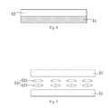
- FIG. 1 is a schematic diagram showing a pixel structure in the related art. As shown in FIG.
- a pixel structure of a Liquid Crystal Display device in the related art includes a plurality of data lines 11 , a plurality of scan lines 12 , a plurality of pixel units 13 formed by intersecting the data lines 11 with the scan lines 12 , TFTs 14 and pixel electrodes 15 disposed in pixel units 13 , where each of the pixel electrodes 15 includes a plurality of slits 151 , and each slit 151 has two corner areas A 1 at both ends thereof (e.g. an upper end and a lower end of the slit as shown in FIG. 1 ).
- a length of the corner area A 1 is limited by the size of the pixel unit 13 , and excessive length of the corner area A 1 will likely cause the break of the pixel electrode 15 .
- Due to the limited length of the corner area A 1 an end of the corner area A 1 cannot be covered by a black matrix in a color filter substrate after the color filter substrate is attached to the array substrate, in this case, an electric field formed at the end of the corner area A 1 controls liquid crystal molecules differently from an electric field formed at the rest part of the slit 151 , thus reduction in light transmittance is caused by the electric field formed at the end of the corner area A 1 , comparing with the electric field formed at the rest part of the slit, in displaying by the Liquid Crystal Display device.
- embodiments of the disclosure provide a pixel structure and a manufacturing method therefor, an array structure, a display panel and a display device, thereby solving the technical problem of the reduction in light transmittance caused by the limited length of a corner area of the slit in the pixel electrode in the related art.
- embodiments of the disclosure provide a pixel structure including:
- embodiments of the disclosure provide a manufacturing method for a pixel structure, which includes the following steps:
- embodiments of the disclosure provide an array substrate including the pixel structure described above.
- embodiments of the disclosure provide the array substrate described in the third example.
- embodiments of the disclosure provide a display device including the display device described in the fourth example.
- a pixel electrode is electrically connected to a TFT in a pixel unit which is in the same row as and adjacently at one side of the pixel electrode, and at least one corner area of the pixel electrode extends toward the TFT electrically connected to the pixel electrode, so that a length of the extended corner area, is increased, and accordingly an end of the corner area is disposed close to the TFT electrically connected to the pixel electrode including the corner area, therefore the end of the corner area can be well covered by a black matrix of a color filter substrate after the color filter substrate is attached to the array substrate, thereby improving the light transmittance.
- FIG. 1 is a schematic diagram showing a pixel structure in the related art
- FIG. 2A is a schematic diagram showing a pixel structure according to embodiments of the disclosure.
- FIG. 2B is a schematic diagram showing a pixel structure according to embodiments of the disclosure.
- FIG. 3A is a schematic diagram showing a pixel structure according to embodiments of the disclosure.
- FIG. 3B is a schematic diagram showing a pixel structure according to embodiments of the disclosure.
- FIG. 4 is a schematic diagram showing a pixel structure according to embodiments of the disclosure.
- FIG. 5 is a flow chart of a method for manufacturing a pixel structure according to embodiments of the disclosure.
- FIG. 6 is a schematic diagram showing an array substrate according to embodiments of the disclosure.
- FIG. 7 is a schematic diagram showing a display panel according to embodiments of the disclosure.
- FIG. 8 is a schematic diagram showing a display device according to embodiments of the disclosure.
- FIG. 2A is a schematic diagram showing a pixel structure according to embodiments of the disclosure.
- the pixel structure includes: a plurality of data lines 21 ; a plurality of scan lines 22 ; a plurality of pixel units 23 formed by intersecting the data lines 21 with the scan lines 22 , where a pixel unit 23 corresponds to one data line 21 and one scan line 22 ; a TFT 24 and a pixel electrode 25 disposed in each of the plurality of pixel units 23 , where the pixel electrode 25 includes a plurality of slits 251 , at least one of which has at least one corner area A 2 at an end thereof, and the pixel electrode 25 in a row is electrically connected to a TFT 24 of a pixel unit 23 , the pixel unit 23 is disposed in the same row as and adjacent to the pixel unit 23 containing the pixel electrode 25 (e.g. at the left side thereof as shown in FIG. 2A
- the display of the pixel unit is realized through the pixel electrode in the pixel unit and the TFT which is electrically connected to the pixel electrode for controlling the pixel electrode.
- the TFT controls the pixel unit in which the pixel electrode is disposed.
- the TFT can be controlled to turn on or off by a scan line which is electrically connected to a gate electrode of the TFT, and a data line which is electrically connected to a source electrode of the TFT may provide the pixel electrode electrically connected to the TFT with a data signal when the TFT is turned on.
- a pixel unit 23 corresponding to one data line 21 and one scan line 22 refers to that the data line 21 corresponding to the pixel unit 23 is the data line 21 electrically connected to the TFT 24 for controlling the pixel unit 23 , and the scan line 22 corresponding to the pixel unit 23 is the scan line 22 electrically connected to the TFT 24 for controlling the pixel unit 23 .
- the pixel electrode 25 in a row is electrically connected to a TFT 24 of a pixel unit 23 , the pixel unit 23 is disposed in the same row as and adjacent to the pixel unit 23 containing the pixel electrode 25 (e.g. at the left side thereof as shown in FIG. 2A ), through a bridging conductive line 252 , which may be made of the same transparent conductive material such as indium tin oxide (ITO) or indium zinc oxide (IZO) as the pixel electrode 25 .
- ITO indium tin oxide
- IZO indium zinc oxide
- At least one corner area A 1 of the pixel electrode 25 may extend along the bridging conductive line 252 toward the TFT 24 which is electrically connected to the pixel electrode 25 .
- a length of the extended corner area A 2 is increased, and an end of the extended corner area A 2 is disposed close to the TFT which is electrically connected to the pixel electrode 25 including the extended corner area A 2 , therefore the end of the corner area A 2 can be well covered by a black matrix in a color filter substrate after the color filter substrate is attached to the array substrate, thereby improving the light transmittance.
- the TFT 24 in order to electrically connect the pixel electrode 25 in a row to the TFT 24 in a pixel unit 23 , the pixel unit is disposed in the same row as and adjacently at the left side of the pixel unit 23 containing the pixel electrode 25 , the TFT 24 is preferably disposed close to the pixel electrode 25 electrically connected to the TFT 24 , thereby conveniently realizing an electrical connection between the TFT 24 and the pixel electrode 25 electrically connected to the TFT 24 and avoiding any interference between the pixel electrode 25 electrically connected to the TFT 24 and a pixel electrode 25 in a pixel unit 23 including the TFT 24 .
- a portion of the data line 21 which is within the pixel unit 23 containing the TFT 24 , is bent so as to match a position of the TFT 24 , and the portion disposes. Since the TFT 24 is disposed close to the pixel electrode 25 electrically connected to the TFT 24 , it is necessary to bend the portion of the corresponding data line 21 within the pixel unit 23 containing the TFT 24 in order to electrically connect the data line 21 with the TFT 24 without shielding the pixel electrode 25 , as shown in FIG. 2A .
- the bent data line 21 in FIG. 2A is an example, and the data line 21 can be otherwise arranged as actually desired as long as the data line 21 is electrically connected to the corresponding TFT 24 without shielding the pixel electrode 25 , which is not limited herein.
- the pixel electrode 25 in a row is electrically connected to a TFT 24 in a pixel unit 23
- the pixel unit 23 is disposed in the same row as and adjacently at the left side of the pixel unit 23 containing the pixel electrode 25 as shown in FIG. 2A
- the pixel electrode 25 may be alternatively electrically connected to a TFT 24 in a pixel unit 23 which is disposed in the same row as and adjacently at the right side of the pixel unit 23 containing the pixel electrode 25 , as shown in FIG. 2B .
- FIG. 2A For the position of the TFT 24 and the arrangement of a data line in the pixel unit 23 containing the TFT 24 in FIG. 2B , reference may be made to the description of FIG. 2A , which will not be repeated herein.
- a source electrode of the TFT 24 is electrically connected to the data line 21 corresponding to a pixel unit 23 , the pixel unit 23 contains a pixel electrode 25 electrically connected to the TFT 24 ; and the gate electrode of the TFT 24 is electrically connected to the scan line 22 corresponding to the pixel unit 23 , the pixel unit 23 contains the pixel electrode 25 electrically connected to the TFT 24 . As shown in FIG.
- the source electrode of the TFT 24 is electrically connected to the data line 21 which is at the left side of a pixel unit 23 including the TFT 24 , and configured for providing a data signal to the pixel electrode 25 which is electrically connected to the TFT 24 ; and the gate electrode of the TFT 24 is electrically connected to the scan line 22 below the pixel unit 23 including the TFT 24 , and configured for controlling the turn-on or turn-off of the pixel unit 23 in which the pixel electrode 25 electrically connected to the TFT 24 is disposed. As shown in FIG.
- the source electrode of the TFT 24 is electrically connected to the data line 21 which is at the right side of the pixel unit 23 including the TFT 24 , and configured for providing a data signal to the pixel electrode 25 which is electrically connected to the TFT 24
- the gate electrode of the TFT 24 is electrically connected to the scan line 22 below the pixel unit 23 including the TFT 24 , and configured for controlling the turn-on or turn-off of the pixel unit 23 in which the pixel electrode 25 electrically connected to the TFT 24 is disposed.
- the pixel units 23 are arranged in an array.
- the pixel units 23 may be arranged in a staggered manner.
- the detailed description of the pixel structure arranged in a staggered manner as shown in FIG. 3A and FIG. 3B may refer to the relevant description of FIG. 2A and FIG. 2B , which will not be repeated herein.
- the pixel electrode 25 in a row is electrically connected to the TFT 24 in a pixel unit 23 , the pixel unit 23 is disposed in the same row as and adjacently at the left side of the pixel unit 23 containing the pixel electrode 25 , such that this pixel electrode 25 partially overlaps with the data line 21 between the pixel electrode 25 and its left adjacent pixel electrode 25 ; as shown in FIG. 2B and FIG.
- the pixel electrode 25 in a row is electrically connected to the TFT 24 in a pixel unit 23 , the pixel unit 23 is disposed in the same row as and adjacently at the right side of the pixel unit 23 containing the pixel electrode 25 , such that the pixel electrode 25 partially overlaps with the data line 21 between the pixel electrode 25 and its right adjacent pixel electrode 25 .
- the pixel structure further includes a common electrode 26 located between the pixel electrode 25 is located and a film layer where a source electrode 242 and a drain electrode 243 of the TFT 24 electrically connected with the pixel electrode 25 are located, and the common electrode 26 is electrically insulated from the pixel electrode 25 by a third insulating layer 273 , and the common electrode 26 is electrically insulated from the source electrode 242 and the drain electrode 243 by a second insulating layer 272 .
- a gate electrode 241 of the TFT 24 is covered by the first insulating layer 271 , and an active layer 244 is disposed above the first insulating layer 271 .
- the source electrode 242 and the drain electrode 243 are disposed at two sides of the active layer 244 and both electrically connected to the active layer 244 .
- the source electrode 242 , the drain electrode 243 and the active layer 244 are insulated from the gate electrode 241 by the first insulating layer 271 , and the source electrode 243 is electrically connected to the pixel electrode 25 .
- the common electrode 26 is disposed between the pixel electrode 25 and the source electrode 242 as well as the drain electrode 243 of the TFT 24 , thereby shielding the electrical signals at the overlap between the pixel electrode 25 and the data line 21 .
- the gate electrode 241 is disposed below the source electrode 242 and the drain electrode 243 in the TFT 24 as shown in FIG. 4 , however such disposal is an example of the arrangement of the gate electrode 241 .
- the gate electrode 241 may be disposed above the source electrode 242 and the drain electrode 243 , which is not limited herein.
- FIG. 5 is a flow chart of a method for manufacturing a pixel structure according to embodiments of the disclosure. As shown in FIG. 5 , the method for manufacturing a pixel structure includes the following Steps 301 to 303 .
- Step 301 a plurality of TFTs are formed
- Each of the formed TFTs includes a gate electrode, a source electrode, a drain electrode and an active area disposed between the drain electrode and the drain electrode, where the gate electrode of the TFT may be disposed above the source electrode and the drain electrode (as in a TFT with a top gate structure), or may be disposed below the source electrode and the drain electrode (as in a TFT with a bottom gate structure), which is not limited herein.
- a plurality of data lines and a plurality of scan lines are formed, where a plurality of pixel units formed by intersecting the data lines with the scan lines, where a pixel unit corresponds to one data line and one scan line and includes one TFT.
- a plurality of pixel electrodes are formed, where a pixel electrode is disposed in one pixel unit and includes a plurality of slits each of which has at least one corner area at an end thereof, the pixel electrode in a row is electrically connected to a TFT in a pixel unit, the pixel unit is disposed in the same row as and adjacently at one side of the pixel unit containing the pixel electrode, and at least one corner area of the pixel electrode extends toward the TFT electrically connected to the pixel electrode.
- FIG. 6 is a schematic diagram showing an array substrate according to embodiments of the disclosure.
- the array substrate includes a glass substrate 41 and a pixel structure 42 , and the pixel structure 42 may be any pixel structure described in the above various embodiments.
- FIG. 7 is a schematic diagram showing a display panel according to embodiments of the disclosure.
- the display panel includes an array substrate 51 , a color filter substrate 52 disposed opposite to the array substrate 51 , and a liquid crystal layer 53 disposed between the array substrate 51 and the color filter substrate 52 , where the liquid crystal layer 53 is made up of liquid crystal molecules 531 .
- the array substrate 51 may be any array substrate described in the above various embodiments.
- the touch sensing function may be an electromagnetic touch sensing function, a capacitive touch sensing function, an electromagnetic capacitive touch sensing function or the like.
- FIG. 8 is a schematic diagram showing a display device according to embodiments of the disclosure.
- the display device 60 includes a display panel 61 , and may further include a drive circuit and other components for supporting a normal operation of the display device 60 .
- the display panel 61 may be any display panel described in the above various embodiments.
- the above display device may be one of a mobile phone, a desktop computer, a notebook computer, a tablet computer and an electronic paper.
- a pixel electrode in a row is electrically connected to a TFT in a pixel unit, the pixel unit is disposed in the same row as and adjacently at one side of a pixel unit containing the pixel electrode, and at least one corner area of the pixel electrode extends toward the TFT electrically connected to the pixel electrode, so that a length of the extended corner area is increased, and accordingly an end of the corner area is disposed close to the TFT electrically connected to the pixel electrode including the corner area, therefore the end of the corner area can be well covered by a black matrix of a color filter substrate after the color filter substrate is attached to the array substrate, thereby improving the light transmittance.
Landscapes
- Physics & Mathematics (AREA)
- Nonlinear Science (AREA)
- General Physics & Mathematics (AREA)
- Chemical & Material Sciences (AREA)
- Crystallography & Structural Chemistry (AREA)
- Mathematical Physics (AREA)
- Optics & Photonics (AREA)
- Engineering & Computer Science (AREA)
- Microelectronics & Electronic Packaging (AREA)
- Geometry (AREA)
- Liquid Crystal (AREA)
- Devices For Indicating Variable Information By Combining Individual Elements (AREA)
- Manufacturing & Machinery (AREA)
Abstract
Description
-
- a plurality of data lines;
- a plurality of scan lines;
- a plurality of pixel units formed by intersecting the plurality of data lines with the plurality of scan lines, where a pixel unit corresponds to one of the data lines and one of the scan lines;
- a TFT and a pixel electrode disposed in each of the pixel units, where the pixel electrode includes a plurality of slits, at least one of which includes at least one corner area at an end thereof;
- where the pixel electrode is electrically connected to a TFT in a pixel unit which is disposed in the same row as and adjacently at one side of a pixel electrode including the pixel electrode, and at least one corner area of the pixel electrode extends toward the TFT electrically connected to the pixel electrode.
-
- forming a plurality of TFTs;
- forming a plurality of data lines and a plurality of scan lines, where a plurality of pixel units are formed by intersecting the plurality of data lines with the plurality of scan lines, and a pixel unit corresponds to one of the data lines and one of the scan lines and includes one of the TFTs; and
- forming a plurality of pixel electrodes, where a pixel electrode is disposed in one pixel unit and includes a plurality of slits, at least one of which includes at least one corner area at an end thereof, and the pixel electrode is electrically connected to a TFT in a pixel unit which is disposed in the same row as and adjacently at one side of a pixel unit comprising the pixel electrode, and at least one corner area of the pixel electrode extends toward the TFT electrically connected to the pixel electrode.
Claims (14)
Applications Claiming Priority (3)
| Application Number | Priority Date | Filing Date | Title |
|---|---|---|---|
| CN201410531284.7 | 2014-10-10 | ||
| CN201410531284 | 2014-10-10 | ||
| CN201410531284.7A CN104317115B (en) | 2014-10-10 | 2014-10-10 | Dot structure and its manufacture method, array base palte, display panel and display device |
Publications (2)
| Publication Number | Publication Date |
|---|---|
| US20160103350A1 US20160103350A1 (en) | 2016-04-14 |
| US9563095B2 true US9563095B2 (en) | 2017-02-07 |
Family
ID=52372366
Family Applications (1)
| Application Number | Title | Priority Date | Filing Date |
|---|---|---|---|
| US14/742,599 Active US9563095B2 (en) | 2014-10-10 | 2015-06-17 | Pixel structure and manufacturing method therefor, array structure, display panel and display device |
Country Status (3)
| Country | Link |
|---|---|
| US (1) | US9563095B2 (en) |
| CN (1) | CN104317115B (en) |
| DE (1) | DE102015110638B4 (en) |
Families Citing this family (7)
| Publication number | Priority date | Publication date | Assignee | Title |
|---|---|---|---|---|
| CN104698696A (en) | 2015-03-26 | 2015-06-10 | 京东方科技集团股份有限公司 | Array substrate, liquid crystal panel and display device |
| CN107479270A (en) * | 2017-08-25 | 2017-12-15 | 上海天马微电子有限公司 | Display panel and display device |
| CN107422562A (en) * | 2017-09-22 | 2017-12-01 | 惠科股份有限公司 | Active switch array substrate |
| TWI676066B (en) * | 2018-01-05 | 2019-11-01 | 友達光電股份有限公司 | Liquid crystal device |
| CN110109305B (en) * | 2019-04-12 | 2020-12-04 | 深圳市华星光电半导体显示技术有限公司 | Display panel |
| CN112147819A (en) * | 2020-09-22 | 2020-12-29 | 南京中电熊猫液晶显示科技有限公司 | Liquid crystal display panel |
| CN114879418A (en) * | 2022-07-11 | 2022-08-09 | 惠科股份有限公司 | Array substrate and display panel |
Citations (3)
| Publication number | Priority date | Publication date | Assignee | Title |
|---|---|---|---|---|
| US20090225267A1 (en) * | 2008-03-06 | 2009-09-10 | Epson Imaging Devices Corporation | Liquid crystal device and electronic apparatus |
| WO2013168566A1 (en) | 2012-05-10 | 2013-11-14 | シャープ株式会社 | Liquid crystal display device |
| JP2014041366A (en) | 2007-12-03 | 2014-03-06 | Semiconductor Energy Lab Co Ltd | Display device |
Family Cites Families (5)
| Publication number | Priority date | Publication date | Assignee | Title |
|---|---|---|---|---|
| US6459464B1 (en) * | 2000-08-14 | 2002-10-01 | Kabushiki Kaisha Advanced Display | Liquid crystal display device with reduced weighting trace defects |
| CN1229682C (en) * | 2002-05-21 | 2005-11-30 | 精工爱普生株式会社 | Electrooptical device and electronic equipment |
| KR100920348B1 (en) * | 2003-02-27 | 2009-10-07 | 삼성전자주식회사 | Liquid crystal display |
| WO2009101732A1 (en) * | 2008-02-15 | 2009-08-20 | Sharp Kabushiki Kaisha | Liquid crystal display device |
| JP5639857B2 (en) | 2010-11-18 | 2014-12-10 | 株式会社ジャパンディスプレイ | Liquid crystal display |
-
2014
- 2014-10-10 CN CN201410531284.7A patent/CN104317115B/en active Active
-
2015
- 2015-06-17 US US14/742,599 patent/US9563095B2/en active Active
- 2015-07-02 DE DE102015110638.8A patent/DE102015110638B4/en active Active
Patent Citations (4)
| Publication number | Priority date | Publication date | Assignee | Title |
|---|---|---|---|---|
| JP2014041366A (en) | 2007-12-03 | 2014-03-06 | Semiconductor Energy Lab Co Ltd | Display device |
| US20090225267A1 (en) * | 2008-03-06 | 2009-09-10 | Epson Imaging Devices Corporation | Liquid crystal device and electronic apparatus |
| WO2013168566A1 (en) | 2012-05-10 | 2013-11-14 | シャープ株式会社 | Liquid crystal display device |
| US20150116644A1 (en) * | 2012-05-10 | 2015-04-30 | Sharp Kabushiki Kaisha | Liquid crystal display device |
Also Published As
| Publication number | Publication date |
|---|---|
| CN104317115B (en) | 2017-11-14 |
| DE102015110638A1 (en) | 2016-04-14 |
| CN104317115A (en) | 2015-01-28 |
| US20160103350A1 (en) | 2016-04-14 |
| DE102015110638B4 (en) | 2019-06-06 |
Similar Documents
| Publication | Publication Date | Title |
|---|---|---|
| US9563095B2 (en) | Pixel structure and manufacturing method therefor, array structure, display panel and display device | |
| US10162450B2 (en) | Array substrate, display panel and display device | |
| KR101978326B1 (en) | Array substrate and manufacturing method and driving method therefor, and display device | |
| US10394354B2 (en) | Array substrate, touch display panel and display apparatus | |
| KR102627941B1 (en) | Touch recognition enabled display device with asymmetric black matrix pattern | |
| US9268190B1 (en) | Pixel structure, manufacturing method of pixel structure, array substrate, and display panel | |
| US10564772B2 (en) | Array substrate, its driving method and manufacturing method, and display device | |
| US9684402B2 (en) | Touch display panel and touch display device | |
| US9933645B2 (en) | Array substrate, display panel, display device and manufacturing method thereof | |
| US9372573B2 (en) | Array substrate, touch panel and driving method thereof | |
| CN106324924B (en) | A kind of array substrate and preparation method thereof, display panel, display device | |
| TWI536235B (en) | Built-in touch panel display device | |
| US10338709B2 (en) | Touch display device with inconspicuous transparent electrodes and electronic apparatus | |
| US9588382B2 (en) | Pixel structure, manufacturing method of pixel structure, array substrate, display panel, and display device | |
| US9213441B2 (en) | In-cell touch panel and liquid crystal device | |
| CN103926742A (en) | Color film substrate and liquid crystal display panel | |
| US20160147343A1 (en) | Touch control display screen and electronic device | |
| US20180181239A1 (en) | Liquid crystal display device with touch sensor and method for driving the same | |
| WO2018232829A1 (en) | Liquid crystal display panel and liquid crystal display device | |
| US10288952B2 (en) | Touch panel, array substrate, and method for fabricating the same | |
| US9665229B2 (en) | Display panel and display device | |
| CN107144999B (en) | Embedded touch screen | |
| KR20170076867A (en) | Liquid crystal display device | |
| WO2019056664A1 (en) | Touch control display device | |
| US8907934B2 (en) | Pixel array substrate and display panel using the same |
Legal Events
| Date | Code | Title | Description |
|---|---|---|---|
| AS | Assignment |
Owner name: TIANMA MICRO-ELECTRONICS CO., LTD., CHINA Free format text: ASSIGNMENT OF ASSIGNORS INTEREST;ASSIGNORS:WANG, TINGHAI;CAO, ZHAOKENG;LIN, YAO;AND OTHERS;REEL/FRAME:036040/0868 Effective date: 20150612 Owner name: SHANGHAI AVIC OPTO ELECTRONICS CO., LTD., CHINA Free format text: ASSIGNMENT OF ASSIGNORS INTEREST;ASSIGNORS:WANG, TINGHAI;CAO, ZHAOKENG;LIN, YAO;AND OTHERS;REEL/FRAME:036040/0868 Effective date: 20150612 |
|
| FEPP | Fee payment procedure |
Free format text: PAYOR NUMBER ASSIGNED (ORIGINAL EVENT CODE: ASPN); ENTITY STATUS OF PATENT OWNER: LARGE ENTITY |
|
| STCF | Information on status: patent grant |
Free format text: PATENTED CASE |
|
| MAFP | Maintenance fee payment |
Free format text: PAYMENT OF MAINTENANCE FEE, 4TH YEAR, LARGE ENTITY (ORIGINAL EVENT CODE: M1551); ENTITY STATUS OF PATENT OWNER: LARGE ENTITY Year of fee payment: 4 |
|
| MAFP | Maintenance fee payment |
Free format text: PAYMENT OF MAINTENANCE FEE, 8TH YEAR, LARGE ENTITY (ORIGINAL EVENT CODE: M1552); ENTITY STATUS OF PATENT OWNER: LARGE ENTITY Year of fee payment: 8 |