US9557869B2 - High-accuracy single-layer capacitive touch panel device with one side for connection - Google Patents
High-accuracy single-layer capacitive touch panel device with one side for connection Download PDFInfo
- Publication number
- US9557869B2 US9557869B2 US14/559,534 US201414559534A US9557869B2 US 9557869 B2 US9557869 B2 US 9557869B2 US 201414559534 A US201414559534 A US 201414559534A US 9557869 B2 US9557869 B2 US 9557869B2
- Authority
- US
- United States
- Prior art keywords
- conductive
- edge
- connection
- triangle sensing
- sensing electrodes
- Prior art date
- Legal status (The legal status is an assumption and is not a legal conclusion. Google has not performed a legal analysis and makes no representation as to the accuracy of the status listed.)
- Expired - Fee Related, expires
Links
Images


Classifications
-
- G—PHYSICS
- G06—COMPUTING OR CALCULATING; COUNTING
- G06F—ELECTRIC DIGITAL DATA PROCESSING
- G06F3/00—Input arrangements for transferring data to be processed into a form capable of being handled by the computer; Output arrangements for transferring data from processing unit to output unit, e.g. interface arrangements
- G06F3/01—Input arrangements or combined input and output arrangements for interaction between user and computer
- G06F3/03—Arrangements for converting the position or the displacement of a member into a coded form
- G06F3/041—Digitisers, e.g. for touch screens or touch pads, characterised by the transducing means
- G06F3/044—Digitisers, e.g. for touch screens or touch pads, characterised by the transducing means by capacitive means
- G06F3/0445—Digitisers, e.g. for touch screens or touch pads, characterised by the transducing means by capacitive means using two or more layers of sensing electrodes, e.g. using two layers of electrodes separated by a dielectric layer
-
- G—PHYSICS
- G06—COMPUTING OR CALCULATING; COUNTING
- G06F—ELECTRIC DIGITAL DATA PROCESSING
- G06F3/00—Input arrangements for transferring data to be processed into a form capable of being handled by the computer; Output arrangements for transferring data from processing unit to output unit, e.g. interface arrangements
- G06F3/01—Input arrangements or combined input and output arrangements for interaction between user and computer
- G06F3/03—Arrangements for converting the position or the displacement of a member into a coded form
- G06F3/041—Digitisers, e.g. for touch screens or touch pads, characterised by the transducing means
- G06F3/044—Digitisers, e.g. for touch screens or touch pads, characterised by the transducing means by capacitive means
- G06F3/0448—Details of the electrode shape, e.g. for enhancing the detection of touches, for generating specific electric field shapes, for enhancing display quality
Definitions
- the present invention relates to a touch panel structure and, more particularly, to a high-accuracy single-layer capacitive touch panel device with one side for connection.
- capacitive touch panels are in widespread use, and are primarily applied in consumer electronic apparatuses, such as PDA, palmtop computer, electronic dictionary, mobile phone, web pad, electronic book, tablet PC, digital camera, self-ordering system, stocktaking machine, POS cash register, credit card POS signature machine, and medical monitoring system.
- a resistive touch panel is formed by overlapping an upper ITO (Indium Tin Oxide) conductive layer and a lower ITO conductive layer.
- the pressure applied to the touch panel will cause the electrodes of the upper layer to conduct with the electrodes of the lower layer.
- a controller calculates the position of the touch point by detecting the voltage variation of the touch panel. When a user touches a certain point on the screen, a current is caused due to the conduction so as to generate an operation, and a processor calculates the position of the operated point, while a driver translates such an operation into the language that the system can understand.
- the single-layer capacitive touch panel device it is arranged to connect the two sides of the conductive layer to a detection circuit for measuring the current and voltage variations on the conductive layer.
- a detection circuit for measuring the current and voltage variations on the conductive layer.
- Such skills can be found in, for example, U.S. Pat. No. 6,961,049 granted to Mulligan, et al. for a “Capacitive touch sensor architecture with unique sensor bar addressing”, and U.S. Pat. No. 7,735,383 granted to Dattalo, et al. for a “Balanced resistance capacitive sensing apparatus”.
- this arrangement needs to dispose the connection wires at two sides of the substrate, resulting in negatively influencing the overall appearance of the touch panel, badly affecting the product design, and erroneously determining the touched point due to the connection wires at the sides.
- FIG. 1 is a schematic diagram of a prior single-layer capacitive touch panel device with one side for connection and its touch detection circuit.
- the prior single-layer capacitive touch panel device 1 includes a substrate 10 , a plurality of conductive lines 101 - 110 , and a touch detection circuit 11 .
- Each of the plurality of conductive lines 101 - 110 is of a bar shape and arranged on the surface of substrate 10 in parallel with each other, and is electrically connected to the touch detection circuit 11 through a connection wire 19 .
- the plurality of conductive lines 101 - 110 are extended from the first side 10 a to the second side 10 b of the substrate 10 .
- Each conductive line 101 - 110 has a connection part 101 b - 110 b close to the second side 10 b .
- the touch detection circuit 11 is electrically connected to the connection part 101 b - 110 b of the conductive lines 101 - 110 through the connection wires 19 , so as to detect the variations of electrical characteristic of the plurality of conductive lines 101 - 110 , thereby determining at least one touch point A on the substrate 10 .
- the touch point detection of FIG. 1 is performed by detecting the capacitance variations of the plurality of conductive lines 101 - 110 to determine the Y-direction coordinate of the touch point A (e.g., the conductive line 108 ), and then detecting the resistance variation of the conductive line 108 , so as to determine the X-direction coordinate of the touch point A.
- Such a detection method encounters a dilemma.
- the width of the conductive line 101 - 110 in increased, the spacing between two conductive lines 101 - 110 is decreased to facilitate in detecting the capacitance variations of the plurality of conductive lines 101 - 110 .
- the width of the conductive line 101110 is increased, the resistance of each of the conductive lines 101 - 110 becomes smaller, resulting in a difficulty in detecting the resistance variations of the conductive lines.
- the width of the conductive line 101 - 110 is decreased, the resistance of each conductive line 101 - 110 is increased to facilitate in detecting the resistance variations of the conductive lines, but the spacing between two conductive lines 101 - 110 is increased and thus the capacitance thereof becomes smaller, which is disadvantageous in detecting the capacitance variations of the conductive lines 101 - 110 .
- the object of the present invention is to provide a high-accuracy single-layer capacitive touch panel device with one side for connection, in which connection wires are disposed at one only side, while the other three sides are designed to have a frameless structure, so as to simplify the arrangement of the touch panel and improve the accuracy of touch point detection.
- a high-accuracy single-layer capacitive touch panel device with one side for connection which comprises: a substrate having a surface, a first side, and a second side opposite to the first side; a plurality of conductive lines, each having an equivalent resistance and an equivalent capacitance, the plurality of conductive lines being arranged in parallel on the surface of the substrate and extended from the first side to the second side of the substrate, each conductive line including a conductive trace having a first edge and a second edge opposite to the first edge and a plurality of triangle sensing electrodes arranged at the two edges of the conductive trace, each triangle sensing electrode being connected with the conductive trace via a connection part, each conductive line only having one connection end close to the second side; and a touch detection circuit electrically connected to the connection ends of the plurality of conductive lines through a connection circuit, so as to detect variations of the equivalent resistances and the equivalent capacitances of the plurality of conductive lines, thereby determining at least one touch position on the
- FIG. 1 is a schematic diagram of a prior single-layer capacitive touch panel device with one side for connection and its touch detection circuit;
- FIG. 2 is a schematic diagram of a high-accuracy single-layer capacitive touch panel device with one side for connection in accordance with a first embodiment of the present invention
- FIG. 3 is a schematic diagram of the conductive lines in accordance with the present invention.
- FIG. 4 is another schematic diagram of the conductive lines in accordance with the present invention.
- FIG. 5 is a schematic diagram of a high-accuracy single-layer capacitive touch panel device with one side for connection in accordance with a second embodiment of the present invention
- FIG. 6 is a schematic diagram of a high-accuracy single-layer capacitive touch panel device with one side for connection in accordance with a third embodiment of the present invention.
- FIG. 7 is a first equivalent circuit in accordance with the present invention.
- FIG. 8 is a second equivalent circuit in accordance with the present invention.
- FIG. 9 is a third equivalent circuit in accordance with the present invention.
- FIG. 10 is a fourth equivalent circuit in accordance with the present invention.
- FIG. 2 is a schematic diagram of a high-accuracy single-layer capacitive touch panel device with one side for connection 200 in accordance with the present invention, which includes a substrate 210 , a plurality of conductive lines 22 - 1 to 22 -N, and a touch detection circuit 230 .
- the substrate 210 includes a surface, a first side 210 a , and a second side 210 b opposite to the first side 210 a .
- the plurality of conductive lines 22 - 1 to 22 -N each has an equivalent resistance and an equivalent capacitance.
- the plurality of conductive lines 22 - 1 to 22 -N are arranged in parallel on the surface of substrate 210 , and extended from the first side 210 a to the second side 210 b of the substrate 210 .
- N conductive lines 22 - 1 to 22 -N there are, for example, N conductive lines 22 - 1 to 22 -N in this embodiment, where N is an integer greater than 1.
- FIG. 3 is a schematic diagram of the conductive lines 22 - 1 to 22 -N in accordance with the present invention.
- Each conductive line has a conductive trace 310 .
- the conductive trace 310 has a first edge and a second edge opposite to the first edge, each edge being arranged with a plurality of triangle sensing electrodes 320 .
- Each triangle sensing electrode 320 has a symmetry axis 3201 and is connected with the conductive trace 310 via a connection part 330 , wherein the connection part 330 is extended along the symmetry axis 3201 of the triangle sensing electrode 320 and has a width (w) smaller than any of side lengths (s 1 , s 2 , s 3 ) of the triangle sensing electrode 320 .
- Each conductive line 22 - 1 to 22 -N only has one connection end 22 - 1 b to 22 -Nb close to the second side 210 b .
- the touch detection circuit 230 is electrically connected to the connection ends 22 - 1 to 22 -Nb of the plurality of conductive lines 22 - 1 to 22 -N through a connection circuit 250 , so as to detect the variations of the equivalent resistances and the equivalent capacitances of the plurality of conductive lines 22 - 1 to 22 -N, thereby determining at least one touch position on the substrate 210 .
- the conductive lines 22 - 1 to 22 -N are made of ITO (Indium Tin Oxide) material
- the connection circuit 250 is a flexible printed circuit (FPC).
- each triangle sensing electrode 320 is symmetric about its symmetry axis 3201 .
- the plurality of triangle sensing electrodes 321 at the first edge of the conductive trace 310 of the i-th conductive line 22 -i are disposed at positions aligned with the positions of the plurality of triangle sensing electrodes 322 at the second edge thereof, respectively, and the symmetry axes 3201 ′ of two adjacent triangle sensing electrodes 321 at the first edge thereof are arranged to have a first distance (2d) therebetween, where i is a positive integer.
- the symmetry axis 3201 ′ of one of the plurality of triangle sensing electrodes 321 at the first edge of the conductive trace 310 of the i-th conductive line 22 -i is arranged at a position to have a second distance (d) to the symmetry axis 3201 ′′ of the nearest one of the plurality of triangle sensing electrodes 323 at the first edge of the conductive trace 310 of the (i+1)-th conductive line 22 -(i+1).
- the first distance (2d) is twice of the second distance (d).
- the symmetry axis 3201 ′′′ of one of the plurality of triangle sensing electrodes 322 at the second edge of the conductive trace 310 of the i-th conductive line 22 -i is arranged at a position to have a second distance (d) to the summetry axis 3201 ′′′′ of the nearest one of the plurality of triangle sensing electrodes 324 at the second edge of the conductive trace 310 of the (i+1)-th conductive line 22 -(i+1).
- FIG. 4 is another schematic diagram of the conductive line 22 - 1 to 22 -N in accordance with the present invention.
- the symmetry axis 3201 ′ of one of the plurality of triangle sensing electrodes 321 at the first edge of the conductive trace 310 of the i-th conductive line 22 -i is arranged at a position to have a third distance (d) to the symmetry axis 3201 ′′′ of the nearest one of the plurality of triangle sensing electrodes 322 at the second edge thereof, and the symmetry axes 3201 ′ of two adjacent triangle sensing electrodes 321 at the first edge are arranged to have a fourth distance (2d) therebetween, wherein the fourth distance (2d) is twice of the third distance (d).
- the plurality of triangle sensing electrodes 321 at the first edge of the conductive trace 310 of the i-th conductive line 22 -i are disposed at positions aligned with the positions of the plurality of triangle sensing electrodes 323 at the first edge of the conductive trace 310 of the (i+1)-th conductive line 22 -(i+1), respectively.
- the plurality of triangle sensing electrodes 322 at the second edge of the conductive trace 310 of the i-th conductive line 22 -i are disposed at positions aligned with the positions of the plurality of triangle sensing electrodes 324 at the second edge of the conductive trace 310 of the (i+1)-th conductive line 22 -(i+1), respectively.
- the touch panel device of the present invention is characterized in that: the conductive line 22 - 1 to 22 -N are arranged is parallel and disposed on the surface of the substrate 210 , and are connected with the connection circuit 250 and the touch detection circuit 230 through the connection ends 22 - 1 b to 22 -Nb at only side.
- the present invention also can adopt a vertical configuration, as shown in FIG. 5 .
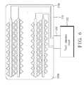
- the present invention can adopt the horizontal configuration but the connection circuit 250 is disposed at the bottom for connection with the touch detection circuit 230 , as shown in FIG. 6 .
- the substrate 210 of the present invention is preferably a rectangle structure, and has the first side 210 a and the second side 210 b opposite to the first side 210 a .
- the plurality of conductive lines 22 - 1 to 22 -N are extended from the first side 210 a to the second side 210 b of the substrate 210 .
- Each conductive line 22 - 1 to 22 -N has a connection end 22 - 1 b to 22 -Nb close to the second side 210 b .
- the touch detection circuit 230 is electrically connected to the connection ends 22 - 1 to 22 -Nb of the conductive lines 22 - 1 to 22 -N through the connection circuit 250 , so as to detect the variations of electrical characteristics of the plurality of conductive line 220 thereby determining at least one touch point A on the substrate 210 .
- the touch detection circuit 230 includes: a multiplexer 231 , a first switch 232 , a second switch 233 , a third switch 234 , a fourth switch 235 , a capacitor 236 , a resistor 237 , an analog to digital converter 238 , an integration circuit 239 , and a micro controller 240 .
- the multiplexer 231 is electrically connected to the plurality of conductive lines 22 - 1 to 22 -N through the connection circuit 250 .
- the first switch 232 has a first terminal “a” connected to the multiplexer 231 , a second terminal “b” connected to a second terminal “b” of the second switch 233 , and a third terminal “c” connected to the capacitor 236 .
- the second switch 233 has a first terminal “a” connected to the resistor 237 and the integration circuit 239 , the second terminal “b” connected to the second terminal “b” of the first switch 232 , and a third terminal “c” connected to the capacitor 236 .
- the third switch 234 has a first terminal “a” connected to the capacitor 236 and the third terminal “c” of the first switch 232 , a second terminal “b” connected to a DC power source V, and a third terminal “c” connected to a second terminal “b” of the fourth switch 235 .
- the fourth switch 235 has a first terminal “a” connected to the analog to digital converter 238 , the second terminal “b” connected to the third terminal “c” of the third switch 234 , and a third terminal “c” connected to the integration circuit 239 .
- the resistor 237 has a resistance R, and the capacitor 236 has a capacitance C.
- Each of the plurality of conductive lines 22 - 1 to 22 -N has an equivalent resistance and an equivalent capacitance.
- the conductive line 22 - 8 is taken as an example in this embodiment.
- the equivalent resistance of the conductive line is R′, and the equivalent capacitance thereof is C′, as shown by the equivalent circuit in FIG. 7 .
- the multiplexer 231 sequentially selects one of the conductive lines 22 - 1 to 22 -N, and thus each conductive line 22 - 1 to 22 -N uses the same way to measure the equivalent resistance and the equivalent capacitance.
- the multiplexer 231 selects the conductive line 22 - 8
- the first terminal “a” of third switch 234 is switched to its second terminal “b” to connect the DC power source V to the capacitor 236
- the first terminal “a” of the second switch 233 is switched to its third terminal “c” to connect the capacitor 236 to the resistor 237 .
- the DC power source V charges the capacitor 236
- the equivalent circuit is shown in FIG. 8 .
- the first terminal “a” of the third switch 234 is switched to its third terminal “c”, and the first terminal “a” of the fourth switch 235 is switched to its second terminal “b” so that the analog to digital converter 238 is electrically connected to the capacitor 236 for reading a voltage value V 1 after charging and then the integration circuit 239 is reset to zero.
- the first terminal “a” of the first switch 232 is switched to its third terminal “c”.
- the first terminal “a” of the second switch 233 is switched to its third terminal “c” so that the capacitor 236 charges the conductive line 228 , and the integration circuit 239 starts to accumulates a square value of the current flowing through the resistor 237 , wherein the equivalent circuit therefor is shown in FIG. 9 .
- the integration circuit 239 continues to accumulate the square value of the current flowing through the resistor 237 .
- the first switch 232 and the first switch 232 are again switched to the capacitor 236 several times so that the capacitor 236 charges the conductive line 228 and the conductive line 228 itself is discharged several times.
- the integration circuit 239 still continues to accumulate the square value of the current flowing through the resistor 237 .
- the integration circuit 239 stops recording the square value of the current flowing through the resistor 237 , and the square value of the total current obtained is I 2 .
- the first terminal “a” of the second switch 233 is switched to its third terminal “c”
- the first terminal “a” of the third switch 234 is switched to its third terminal “c”
- the first terminal “a” of the fourth switch 235 is switched to its second terminal “b”, so as to connect the analog to digital converter 238 to the capacitor 236 for reading the voltage value V 2 of the capacitor 236 after discharging.
- the analog to digital converter 238 transmits the first voltage value V 1 , the second voltage value V 2 and the total current value I to the micro controller 240 for calculating the equivalent resistance R′ and the equivalent capacitance C′ of the conductive line 22 - 8 according to the law of conservation of energy.
- the calculation is based on the following formulas:
- the equivalent capacitance C′ of the conductive line 22 - 8 is increased, and thus is obviously higher than those of the other conductive lines 22 - 1 to 22 -N.
- the coordinate of the vertical axis can be obtained, from which the micro controller 240 can determine that the touch point A is on the conductive line 22 - 8 .
- the equivalent resistance R′ is positively proportional to the distance between the touch point A and the connection end 22 - 8 b . Therefore, with the positive proportion, it is able to calculate the coordinate of horizontal axis of the touch point A on the conductive line 22 - 8 . Accordingly, by reading the first voltage value V 1 , the second voltage value V 2 and the current value I, the micro controller 240 can determine the plane coordinate of the touch point A on the substrate 210 .
- the area of the triangle sensing electrodes 322 of conductive trace 310 of the i-th conductive line 22 -i and the triangle sensing electrodes 323 of conductive trace 310 of the (i+1)-th conductive line 22 -(i+1) is effectively increased, which facilitates the touch detection circuit 230 to detect the capacitance variations of the plurality of conductive lines 22 - 1 to 22 -N.
- the conductive trace 310 of the conductive line can be made thin to increase the resistance value of the conductive trace 310 for allowing the touch detection circuit 230 to detect the resistance variation of the conductive trace 310 .
- the accuracy of detecting the touch position in accordance with the present invention is higher than that of the prior art.
Landscapes
- Engineering & Computer Science (AREA)
- General Engineering & Computer Science (AREA)
- Theoretical Computer Science (AREA)
- Human Computer Interaction (AREA)
- Physics & Mathematics (AREA)
- General Physics & Mathematics (AREA)
- Quality & Reliability (AREA)
- Position Input By Displaying (AREA)
Abstract
Description
Claims (6)
Applications Claiming Priority (3)
| Application Number | Priority Date | Filing Date | Title |
|---|---|---|---|
| TW102222763U TWM480114U (en) | 2013-12-04 | 2013-12-04 | Single-sided single-layered capacitive touch panel device with high accuracy |
| TW102222763 | 2013-12-04 | ||
| TW102222763U | 2013-12-04 |
Publications (2)
| Publication Number | Publication Date |
|---|---|
| US20150153879A1 US20150153879A1 (en) | 2015-06-04 |
| US9557869B2 true US9557869B2 (en) | 2017-01-31 |
Family
ID=51395408
Family Applications (1)
| Application Number | Title | Priority Date | Filing Date |
|---|---|---|---|
| US14/559,534 Expired - Fee Related US9557869B2 (en) | 2013-12-04 | 2014-12-03 | High-accuracy single-layer capacitive touch panel device with one side for connection |
Country Status (3)
| Country | Link |
|---|---|
| US (1) | US9557869B2 (en) |
| CN (1) | CN204331671U (en) |
| TW (1) | TWM480114U (en) |
Families Citing this family (1)
| Publication number | Priority date | Publication date | Assignee | Title |
|---|---|---|---|---|
| CN115826798A (en) * | 2022-11-30 | 2023-03-21 | 深圳市华科创智技术有限公司 | A High Reliability Nano Silver Capacitive Screen |
Citations (5)
| Publication number | Priority date | Publication date | Assignee | Title |
|---|---|---|---|---|
| US20070247443A1 (en) * | 2006-04-25 | 2007-10-25 | Harald Philipp | Hybrid Capacitive Touch Screen Element |
| US20110095990A1 (en) * | 2009-10-23 | 2011-04-28 | Harald Philipp | Interdigitated touchscreen electrodes |
| US20130154997A1 (en) * | 2011-12-16 | 2013-06-20 | Silicon Integrated Systems Corp. | Sensing device, touch sensing system, and display device |
| US20130162565A1 (en) * | 2011-12-21 | 2013-06-27 | Interflex Co., Ltd. | Touch sensor panel using oscillation frequency |
| US20150092121A1 (en) * | 2013-09-30 | 2015-04-02 | Elan Microelectronics Corporation | Capacitive touch panel and electrode set thereof |
-
2013
- 2013-12-04 TW TW102222763U patent/TWM480114U/en not_active IP Right Cessation
-
2014
- 2014-11-04 CN CN201420653790.9U patent/CN204331671U/en not_active Expired - Fee Related
- 2014-12-03 US US14/559,534 patent/US9557869B2/en not_active Expired - Fee Related
Patent Citations (5)
| Publication number | Priority date | Publication date | Assignee | Title |
|---|---|---|---|---|
| US20070247443A1 (en) * | 2006-04-25 | 2007-10-25 | Harald Philipp | Hybrid Capacitive Touch Screen Element |
| US20110095990A1 (en) * | 2009-10-23 | 2011-04-28 | Harald Philipp | Interdigitated touchscreen electrodes |
| US20130154997A1 (en) * | 2011-12-16 | 2013-06-20 | Silicon Integrated Systems Corp. | Sensing device, touch sensing system, and display device |
| US20130162565A1 (en) * | 2011-12-21 | 2013-06-27 | Interflex Co., Ltd. | Touch sensor panel using oscillation frequency |
| US20150092121A1 (en) * | 2013-09-30 | 2015-04-02 | Elan Microelectronics Corporation | Capacitive touch panel and electrode set thereof |
Also Published As
| Publication number | Publication date |
|---|---|
| US20150153879A1 (en) | 2015-06-04 |
| CN204331671U (en) | 2015-05-13 |
| TWM480114U (en) | 2014-06-11 |
Similar Documents
| Publication | Publication Date | Title |
|---|---|---|
| EP4216043B1 (en) | Open close detection of foldable phone lid angle calculation | |
| US8144132B2 (en) | Multipoint sensing method for capacitive touch panel | |
| US8860686B2 (en) | Multi-chip touch screens | |
| US10754457B2 (en) | Touch-screen panel with multiple sense units and related methods | |
| US8970529B2 (en) | Touch sensor panel using oscillation frequency | |
| TWI621986B (en) | Pressure sensing touch display device | |
| US20100026655A1 (en) | Capacitive Touchscreen or Touchpad for Finger or Stylus | |
| CN105117058B (en) | A kind of touch panel, touch-control display panel and electronic equipment | |
| US20120182252A1 (en) | Differential Capacitive Touchscreen or Touch Panel | |
| US9134870B2 (en) | Capacitive touch-sensitive panel and mobile terminal using the same | |
| CN102473044A (en) | Capacitance type touch panel | |
| JP2015049895A (en) | Input signal identification method of touch panel | |
| US20140320451A1 (en) | Apparatus and method for detecting adjacent object and method of driving electronic device | |
| CN104375730A (en) | Touch panel and touch display device | |
| CN104750333B (en) | Touch device and method for updating reference two-dimensional sensing information thereof | |
| US9557869B2 (en) | High-accuracy single-layer capacitive touch panel device with one side for connection | |
| CN103455195A (en) | Touch screen device | |
| TWI470496B (en) | Method of sampling touch points for touch panel | |
| KR20150017123A (en) | Touch sensor and drinving method thereof | |
| CN102841719A (en) | Structure of capacitive touch screen sensor | |
| CN103488358A (en) | Touch panel | |
| CN102830884A (en) | Capacitive touch screen sensor | |
| KR101308965B1 (en) | Single Layer Capacitive Type Touch Screen Device | |
| CN108700974B (en) | Capacitance detection circuit and electronic device | |
| CN202838290U (en) | Multi-touch capacitive touch screen |
Legal Events
| Date | Code | Title | Description |
|---|---|---|---|
| AS | Assignment |
Owner name: SUPERC-TOUCH CORPORATION, TAIWAN Free format text: ASSIGNMENT OF ASSIGNORS INTEREST;ASSIGNOR:LEE, HSIANG-YU;REEL/FRAME:034515/0057 Effective date: 20141124 |
|
| STCF | Information on status: patent grant |
Free format text: PATENTED CASE |
|
| MAFP | Maintenance fee payment |
Free format text: PAYMENT OF MAINTENANCE FEE, 4TH YR, SMALL ENTITY (ORIGINAL EVENT CODE: M2551); ENTITY STATUS OF PATENT OWNER: SMALL ENTITY Year of fee payment: 4 |
|
| FEPP | Fee payment procedure |
Free format text: MAINTENANCE FEE REMINDER MAILED (ORIGINAL EVENT CODE: REM.); ENTITY STATUS OF PATENT OWNER: SMALL ENTITY |
|
| LAPS | Lapse for failure to pay maintenance fees |
Free format text: PATENT EXPIRED FOR FAILURE TO PAY MAINTENANCE FEES (ORIGINAL EVENT CODE: EXP.); ENTITY STATUS OF PATENT OWNER: SMALL ENTITY |
|
| STCH | Information on status: patent discontinuation |
Free format text: PATENT EXPIRED DUE TO NONPAYMENT OF MAINTENANCE FEES UNDER 37 CFR 1.362 |
|
| FP | Lapsed due to failure to pay maintenance fee |
Effective date: 20250131 |