US9548210B2 - Fabrication method of a transistor with improved field effect - Google Patents
Fabrication method of a transistor with improved field effect Download PDFInfo
- Publication number
- US9548210B2 US9548210B2 US14/695,787 US201514695787A US9548210B2 US 9548210 B2 US9548210 B2 US 9548210B2 US 201514695787 A US201514695787 A US 201514695787A US 9548210 B2 US9548210 B2 US 9548210B2
- Authority
- US
- United States
- Prior art keywords
- source
- metallic material
- semiconductor material
- fabrication method
- drain areas
- Prior art date
- Legal status (The legal status is an assumption and is not a legal conclusion. Google has not performed a legal analysis and makes no representation as to the accuracy of the status listed.)
- Active
Links
- 238000004519 manufacturing process Methods 0.000 title claims abstract description 27
- 230000005669 field effect Effects 0.000 title claims abstract description 9
- 238000000034 method Methods 0.000 title claims description 38
- 239000000463 material Substances 0.000 claims abstract description 105
- 239000004065 semiconductor Substances 0.000 claims abstract description 75
- 239000007769 metal material Substances 0.000 claims abstract description 74
- 230000004888 barrier function Effects 0.000 claims abstract description 48
- 239000000758 substrate Substances 0.000 claims abstract description 24
- 238000010438 heat treatment Methods 0.000 claims abstract description 8
- 238000000151 deposition Methods 0.000 claims description 55
- 230000008021 deposition Effects 0.000 claims description 37
- 229910045601 alloy Inorganic materials 0.000 claims description 36
- 239000000956 alloy Substances 0.000 claims description 36
- 239000004020 conductor Substances 0.000 claims description 25
- PXHVJJICTQNCMI-UHFFFAOYSA-N Nickel Chemical compound [Ni] PXHVJJICTQNCMI-UHFFFAOYSA-N 0.000 claims description 24
- BASFCYQUMIYNBI-UHFFFAOYSA-N platinum Chemical compound [Pt] BASFCYQUMIYNBI-UHFFFAOYSA-N 0.000 claims description 20
- XUIMIQQOPSSXEZ-UHFFFAOYSA-N Silicon Chemical compound [Si] XUIMIQQOPSSXEZ-UHFFFAOYSA-N 0.000 claims description 19
- 229910052710 silicon Inorganic materials 0.000 claims description 19
- 239000010703 silicon Substances 0.000 claims description 19
- KDLHZDBZIXYQEI-UHFFFAOYSA-N Palladium Chemical compound [Pd] KDLHZDBZIXYQEI-UHFFFAOYSA-N 0.000 claims description 18
- 229910052721 tungsten Inorganic materials 0.000 claims description 13
- 229910052759 nickel Inorganic materials 0.000 claims description 12
- WFKWXMTUELFFGS-UHFFFAOYSA-N tungsten Chemical compound [W] WFKWXMTUELFFGS-UHFFFAOYSA-N 0.000 claims description 12
- 239000010937 tungsten Substances 0.000 claims description 12
- 229910017052 cobalt Inorganic materials 0.000 claims description 11
- 239000010941 cobalt Substances 0.000 claims description 11
- GUTLYIVDDKVIGB-UHFFFAOYSA-N cobalt atom Chemical compound [Co] GUTLYIVDDKVIGB-UHFFFAOYSA-N 0.000 claims description 11
- RTAQQCXQSZGOHL-UHFFFAOYSA-N Titanium Chemical compound [Ti] RTAQQCXQSZGOHL-UHFFFAOYSA-N 0.000 claims description 10
- 229910052697 platinum Inorganic materials 0.000 claims description 10
- 239000010936 titanium Substances 0.000 claims description 10
- 229910052719 titanium Inorganic materials 0.000 claims description 10
- ZOKXTWBITQBERF-UHFFFAOYSA-N Molybdenum Chemical compound [Mo] ZOKXTWBITQBERF-UHFFFAOYSA-N 0.000 claims description 9
- 229910052750 molybdenum Inorganic materials 0.000 claims description 9
- 239000011733 molybdenum Substances 0.000 claims description 9
- 229910052763 palladium Inorganic materials 0.000 claims description 9
- 229910052715 tantalum Inorganic materials 0.000 claims description 9
- GUVRBAGPIYLISA-UHFFFAOYSA-N tantalum atom Chemical compound [Ta] GUVRBAGPIYLISA-UHFFFAOYSA-N 0.000 claims description 9
- 239000007787 solid Substances 0.000 claims description 7
- OKTJSMMVPCPJKN-UHFFFAOYSA-N Carbon Chemical compound [C] OKTJSMMVPCPJKN-UHFFFAOYSA-N 0.000 claims description 5
- 229910052799 carbon Inorganic materials 0.000 claims description 5
- 238000005498 polishing Methods 0.000 claims description 3
- 239000000126 substance Substances 0.000 claims description 3
- HMDDXIMCDZRSNE-UHFFFAOYSA-N [C].[Si] Chemical compound [C].[Si] HMDDXIMCDZRSNE-UHFFFAOYSA-N 0.000 claims 1
- 238000006243 chemical reaction Methods 0.000 abstract description 8
- 230000009466 transformation Effects 0.000 abstract 1
- 238000000137 annealing Methods 0.000 description 13
- 230000015572 biosynthetic process Effects 0.000 description 12
- 229910052751 metal Inorganic materials 0.000 description 8
- 239000002184 metal Substances 0.000 description 8
- 229910052581 Si3N4 Inorganic materials 0.000 description 7
- 238000005229 chemical vapour deposition Methods 0.000 description 7
- HQVNEWCFYHHQES-UHFFFAOYSA-N silicon nitride Chemical compound N12[Si]34N5[Si]62N3[Si]51N64 HQVNEWCFYHHQES-UHFFFAOYSA-N 0.000 description 7
- VYPSYNLAJGMNEJ-UHFFFAOYSA-N Silicium dioxide Chemical compound O=[Si]=O VYPSYNLAJGMNEJ-UHFFFAOYSA-N 0.000 description 5
- 238000009413 insulation Methods 0.000 description 5
- 229910052814 silicon oxide Inorganic materials 0.000 description 5
- 229910000577 Silicon-germanium Inorganic materials 0.000 description 4
- 238000005530 etching Methods 0.000 description 4
- LEVVHYCKPQWKOP-UHFFFAOYSA-N [Si].[Ge] Chemical compound [Si].[Ge] LEVVHYCKPQWKOP-UHFFFAOYSA-N 0.000 description 3
- 239000012777 electrically insulating material Substances 0.000 description 3
- 239000012212 insulator Substances 0.000 description 3
- 150000002736 metal compounds Chemical class 0.000 description 3
- 238000005240 physical vapour deposition Methods 0.000 description 3
- 230000009467 reduction Effects 0.000 description 3
- 229910021332 silicide Inorganic materials 0.000 description 3
- FVBUAEGBCNSCDD-UHFFFAOYSA-N silicide(4-) Chemical compound [Si-4] FVBUAEGBCNSCDD-UHFFFAOYSA-N 0.000 description 3
- IJGRMHOSHXDMSA-UHFFFAOYSA-N Atomic nitrogen Chemical compound N#N IJGRMHOSHXDMSA-UHFFFAOYSA-N 0.000 description 2
- BOTDANWDWHJENH-UHFFFAOYSA-N Tetraethyl orthosilicate Chemical compound CCO[Si](OCC)(OCC)OCC BOTDANWDWHJENH-UHFFFAOYSA-N 0.000 description 2
- ATJFFYVFTNAWJD-UHFFFAOYSA-N Tin Chemical compound [Sn] ATJFFYVFTNAWJD-UHFFFAOYSA-N 0.000 description 2
- 238000000231 atomic layer deposition Methods 0.000 description 2
- 230000008859 change Effects 0.000 description 2
- 239000002800 charge carrier Substances 0.000 description 2
- 229910052802 copper Inorganic materials 0.000 description 2
- 239000010949 copper Substances 0.000 description 2
- 230000000694 effects Effects 0.000 description 2
- 229910052732 germanium Inorganic materials 0.000 description 2
- GNPVGFCGXDBREM-UHFFFAOYSA-N germanium atom Chemical compound [Ge] GNPVGFCGXDBREM-UHFFFAOYSA-N 0.000 description 2
- 238000002955 isolation Methods 0.000 description 2
- 230000004807 localization Effects 0.000 description 2
- 150000002739 metals Chemical class 0.000 description 2
- 239000000203 mixture Substances 0.000 description 2
- 230000007935 neutral effect Effects 0.000 description 2
- 229910019001 CoSi Inorganic materials 0.000 description 1
- 229910018999 CoSi2 Inorganic materials 0.000 description 1
- RYGMFSIKBFXOCR-UHFFFAOYSA-N Copper Chemical compound [Cu] RYGMFSIKBFXOCR-UHFFFAOYSA-N 0.000 description 1
- 229910000990 Ni alloy Inorganic materials 0.000 description 1
- 229910005883 NiSi Inorganic materials 0.000 description 1
- 238000005280 amorphization Methods 0.000 description 1
- QVGXLLKOCUKJST-UHFFFAOYSA-N atomic oxygen Chemical compound [O] QVGXLLKOCUKJST-UHFFFAOYSA-N 0.000 description 1
- 230000000903 blocking effect Effects 0.000 description 1
- 125000004432 carbon atom Chemical group C* 0.000 description 1
- 239000000969 carrier Substances 0.000 description 1
- 150000001875 compounds Chemical class 0.000 description 1
- 239000003989 dielectric material Substances 0.000 description 1
- 238000004070 electrodeposition Methods 0.000 description 1
- 230000008030 elimination Effects 0.000 description 1
- 238000003379 elimination reaction Methods 0.000 description 1
- 230000009969 flowable effect Effects 0.000 description 1
- SCCCLDWUZODEKG-UHFFFAOYSA-N germanide Chemical compound [GeH3-] SCCCLDWUZODEKG-UHFFFAOYSA-N 0.000 description 1
- 238000005468 ion implantation Methods 0.000 description 1
- 229910001092 metal group alloy Inorganic materials 0.000 description 1
- 230000004048 modification Effects 0.000 description 1
- 238000012986 modification Methods 0.000 description 1
- 150000004767 nitrides Chemical class 0.000 description 1
- 229910052757 nitrogen Inorganic materials 0.000 description 1
- 229910052760 oxygen Inorganic materials 0.000 description 1
- 239000001301 oxygen Substances 0.000 description 1
- 125000004430 oxygen atom Chemical group O* 0.000 description 1
- 238000000206 photolithography Methods 0.000 description 1
- 125000006850 spacer group Chemical group 0.000 description 1
- 238000011426 transformation method Methods 0.000 description 1
Images


Classifications
-
- H—ELECTRICITY
- H01—ELECTRIC ELEMENTS
- H01L—SEMICONDUCTOR DEVICES NOT COVERED BY CLASS H10
- H01L21/00—Processes or apparatus adapted for the manufacture or treatment of semiconductor or solid state devices or of parts thereof
- H01L21/02—Manufacture or treatment of semiconductor devices or of parts thereof
- H01L21/04—Manufacture or treatment of semiconductor devices or of parts thereof the devices having at least one potential-jump barrier or surface barrier, e.g. PN junction, depletion layer or carrier concentration layer
- H01L21/18—Manufacture or treatment of semiconductor devices or of parts thereof the devices having at least one potential-jump barrier or surface barrier, e.g. PN junction, depletion layer or carrier concentration layer the devices having semiconductor bodies comprising elements of Group IV of the Periodic System or AIIIBV compounds with or without impurities, e.g. doping materials
- H01L21/30—Treatment of semiconductor bodies using processes or apparatus not provided for in groups H01L21/20 - H01L21/26
- H01L21/31—Treatment of semiconductor bodies using processes or apparatus not provided for in groups H01L21/20 - H01L21/26 to form insulating layers thereon, e.g. for masking or by using photolithographic techniques; After treatment of these layers; Selection of materials for these layers
- H01L21/3105—After-treatment
- H01L21/31051—Planarisation of the insulating layers
-
- H—ELECTRICITY
- H01—ELECTRIC ELEMENTS
- H01L—SEMICONDUCTOR DEVICES NOT COVERED BY CLASS H10
- H01L21/00—Processes or apparatus adapted for the manufacture or treatment of semiconductor or solid state devices or of parts thereof
- H01L21/02—Manufacture or treatment of semiconductor devices or of parts thereof
- H01L21/04—Manufacture or treatment of semiconductor devices or of parts thereof the devices having at least one potential-jump barrier or surface barrier, e.g. PN junction, depletion layer or carrier concentration layer
- H01L21/18—Manufacture or treatment of semiconductor devices or of parts thereof the devices having at least one potential-jump barrier or surface barrier, e.g. PN junction, depletion layer or carrier concentration layer the devices having semiconductor bodies comprising elements of Group IV of the Periodic System or AIIIBV compounds with or without impurities, e.g. doping materials
- H01L21/28—Manufacture of electrodes on semiconductor bodies using processes or apparatus not provided for in groups H01L21/20 - H01L21/268
- H01L21/283—Deposition of conductive or insulating materials for electrodes conducting electric current
- H01L21/285—Deposition of conductive or insulating materials for electrodes conducting electric current from a gas or vapour, e.g. condensation
- H01L21/28506—Deposition of conductive or insulating materials for electrodes conducting electric current from a gas or vapour, e.g. condensation of conductive layers
- H01L21/28512—Deposition of conductive or insulating materials for electrodes conducting electric current from a gas or vapour, e.g. condensation of conductive layers on semiconductor bodies comprising elements of Group IV of the Periodic System
- H01L21/28518—Deposition of conductive or insulating materials for electrodes conducting electric current from a gas or vapour, e.g. condensation of conductive layers on semiconductor bodies comprising elements of Group IV of the Periodic System the conductive layers comprising silicides
-
- H—ELECTRICITY
- H01—ELECTRIC ELEMENTS
- H01L—SEMICONDUCTOR DEVICES NOT COVERED BY CLASS H10
- H01L21/00—Processes or apparatus adapted for the manufacture or treatment of semiconductor or solid state devices or of parts thereof
- H01L21/70—Manufacture or treatment of devices consisting of a plurality of solid state components formed in or on a common substrate or of parts thereof; Manufacture of integrated circuit devices or of parts thereof
- H01L21/71—Manufacture of specific parts of devices defined in group H01L21/70
- H01L21/768—Applying interconnections to be used for carrying current between separate components within a device comprising conductors and dielectrics
- H01L21/76838—Applying interconnections to be used for carrying current between separate components within a device comprising conductors and dielectrics characterised by the formation and the after-treatment of the conductors
- H01L21/76841—Barrier, adhesion or liner layers
- H01L21/76843—Barrier, adhesion or liner layers formed in openings in a dielectric
-
- H—ELECTRICITY
- H01—ELECTRIC ELEMENTS
- H01L—SEMICONDUCTOR DEVICES NOT COVERED BY CLASS H10
- H01L21/00—Processes or apparatus adapted for the manufacture or treatment of semiconductor or solid state devices or of parts thereof
- H01L21/70—Manufacture or treatment of devices consisting of a plurality of solid state components formed in or on a common substrate or of parts thereof; Manufacture of integrated circuit devices or of parts thereof
- H01L21/71—Manufacture of specific parts of devices defined in group H01L21/70
- H01L21/768—Applying interconnections to be used for carrying current between separate components within a device comprising conductors and dielectrics
- H01L21/76838—Applying interconnections to be used for carrying current between separate components within a device comprising conductors and dielectrics characterised by the formation and the after-treatment of the conductors
- H01L21/76841—Barrier, adhesion or liner layers
- H01L21/76853—Barrier, adhesion or liner layers characterized by particular after-treatment steps
- H01L21/76855—After-treatment introducing at least one additional element into the layer
-
- H—ELECTRICITY
- H01—ELECTRIC ELEMENTS
- H01L—SEMICONDUCTOR DEVICES NOT COVERED BY CLASS H10
- H01L21/00—Processes or apparatus adapted for the manufacture or treatment of semiconductor or solid state devices or of parts thereof
- H01L21/70—Manufacture or treatment of devices consisting of a plurality of solid state components formed in or on a common substrate or of parts thereof; Manufacture of integrated circuit devices or of parts thereof
- H01L21/71—Manufacture of specific parts of devices defined in group H01L21/70
- H01L21/768—Applying interconnections to be used for carrying current between separate components within a device comprising conductors and dielectrics
- H01L21/76838—Applying interconnections to be used for carrying current between separate components within a device comprising conductors and dielectrics characterised by the formation and the after-treatment of the conductors
- H01L21/76877—Filling of holes, grooves or trenches, e.g. vias, with conductive material
- H01L21/76883—Post-treatment or after-treatment of the conductive material
-
- H—ELECTRICITY
- H01—ELECTRIC ELEMENTS
- H01L—SEMICONDUCTOR DEVICES NOT COVERED BY CLASS H10
- H01L21/00—Processes or apparatus adapted for the manufacture or treatment of semiconductor or solid state devices or of parts thereof
- H01L21/70—Manufacture or treatment of devices consisting of a plurality of solid state components formed in or on a common substrate or of parts thereof; Manufacture of integrated circuit devices or of parts thereof
- H01L21/77—Manufacture or treatment of devices consisting of a plurality of solid state components or integrated circuits formed in, or on, a common substrate
- H01L21/78—Manufacture or treatment of devices consisting of a plurality of solid state components or integrated circuits formed in, or on, a common substrate with subsequent division of the substrate into plural individual devices
- H01L21/82—Manufacture or treatment of devices consisting of a plurality of solid state components or integrated circuits formed in, or on, a common substrate with subsequent division of the substrate into plural individual devices to produce devices, e.g. integrated circuits, each consisting of a plurality of components
- H01L21/822—Manufacture or treatment of devices consisting of a plurality of solid state components or integrated circuits formed in, or on, a common substrate with subsequent division of the substrate into plural individual devices to produce devices, e.g. integrated circuits, each consisting of a plurality of components the substrate being a semiconductor, using silicon technology
- H01L21/8232—Field-effect technology
- H01L21/8234—MIS technology, i.e. integration processes of field effect transistors of the conductor-insulator-semiconductor type
- H01L21/8238—Complementary field-effect transistors, e.g. CMOS
- H01L21/823807—Complementary field-effect transistors, e.g. CMOS with a particular manufacturing method of the channel structures, e.g. channel implants, halo or pocket implants, or channel materials
-
- H—ELECTRICITY
- H01—ELECTRIC ELEMENTS
- H01L—SEMICONDUCTOR DEVICES NOT COVERED BY CLASS H10
- H01L21/00—Processes or apparatus adapted for the manufacture or treatment of semiconductor or solid state devices or of parts thereof
- H01L21/70—Manufacture or treatment of devices consisting of a plurality of solid state components formed in or on a common substrate or of parts thereof; Manufacture of integrated circuit devices or of parts thereof
- H01L21/77—Manufacture or treatment of devices consisting of a plurality of solid state components or integrated circuits formed in, or on, a common substrate
- H01L21/78—Manufacture or treatment of devices consisting of a plurality of solid state components or integrated circuits formed in, or on, a common substrate with subsequent division of the substrate into plural individual devices
- H01L21/82—Manufacture or treatment of devices consisting of a plurality of solid state components or integrated circuits formed in, or on, a common substrate with subsequent division of the substrate into plural individual devices to produce devices, e.g. integrated circuits, each consisting of a plurality of components
- H01L21/822—Manufacture or treatment of devices consisting of a plurality of solid state components or integrated circuits formed in, or on, a common substrate with subsequent division of the substrate into plural individual devices to produce devices, e.g. integrated circuits, each consisting of a plurality of components the substrate being a semiconductor, using silicon technology
- H01L21/8232—Field-effect technology
- H01L21/8234—MIS technology, i.e. integration processes of field effect transistors of the conductor-insulator-semiconductor type
- H01L21/8238—Complementary field-effect transistors, e.g. CMOS
- H01L21/823814—Complementary field-effect transistors, e.g. CMOS with a particular manufacturing method of the source or drain structures, e.g. specific source or drain implants or silicided source or drain structures or raised source or drain structures
-
- H—ELECTRICITY
- H01—ELECTRIC ELEMENTS
- H01L—SEMICONDUCTOR DEVICES NOT COVERED BY CLASS H10
- H01L29/00—Semiconductor devices adapted for rectifying, amplifying, oscillating or switching, or capacitors or resistors with at least one potential-jump barrier or surface barrier, e.g. PN junction depletion layer or carrier concentration layer; Details of semiconductor bodies or of electrodes thereof ; Multistep manufacturing processes therefor
- H01L29/66—Types of semiconductor device ; Multistep manufacturing processes therefor
- H01L29/68—Types of semiconductor device ; Multistep manufacturing processes therefor controllable by only the electric current supplied, or only the electric potential applied, to an electrode which does not carry the current to be rectified, amplified or switched
- H01L29/76—Unipolar devices, e.g. field effect transistors
- H01L29/772—Field effect transistors
- H01L29/78—Field effect transistors with field effect produced by an insulated gate
- H01L29/7842—Field effect transistors with field effect produced by an insulated gate means for exerting mechanical stress on the crystal lattice of the channel region, e.g. using a flexible substrate
- H01L29/7845—Field effect transistors with field effect produced by an insulated gate means for exerting mechanical stress on the crystal lattice of the channel region, e.g. using a flexible substrate the means being a conductive material, e.g. silicided S/D or Gate
-
- H—ELECTRICITY
- H01—ELECTRIC ELEMENTS
- H01L—SEMICONDUCTOR DEVICES NOT COVERED BY CLASS H10
- H01L29/00—Semiconductor devices adapted for rectifying, amplifying, oscillating or switching, or capacitors or resistors with at least one potential-jump barrier or surface barrier, e.g. PN junction depletion layer or carrier concentration layer; Details of semiconductor bodies or of electrodes thereof ; Multistep manufacturing processes therefor
- H01L29/66—Types of semiconductor device ; Multistep manufacturing processes therefor
- H01L29/66007—Multistep manufacturing processes
- H01L29/66075—Multistep manufacturing processes of devices having semiconductor bodies comprising group 14 or group 13/15 materials
- H01L29/66227—Multistep manufacturing processes of devices having semiconductor bodies comprising group 14 or group 13/15 materials the devices being controllable only by the electric current supplied or the electric potential applied, to an electrode which does not carry the current to be rectified, amplified or switched, e.g. three-terminal devices
- H01L29/66409—Unipolar field-effect transistors
- H01L29/66477—Unipolar field-effect transistors with an insulated gate, i.e. MISFET
- H01L29/665—Unipolar field-effect transistors with an insulated gate, i.e. MISFET using self aligned silicidation, i.e. salicide
-
- H—ELECTRICITY
- H01—ELECTRIC ELEMENTS
- H01L—SEMICONDUCTOR DEVICES NOT COVERED BY CLASS H10
- H01L29/00—Semiconductor devices adapted for rectifying, amplifying, oscillating or switching, or capacitors or resistors with at least one potential-jump barrier or surface barrier, e.g. PN junction depletion layer or carrier concentration layer; Details of semiconductor bodies or of electrodes thereof ; Multistep manufacturing processes therefor
- H01L29/66—Types of semiconductor device ; Multistep manufacturing processes therefor
- H01L29/66007—Multistep manufacturing processes
- H01L29/66075—Multistep manufacturing processes of devices having semiconductor bodies comprising group 14 or group 13/15 materials
- H01L29/66227—Multistep manufacturing processes of devices having semiconductor bodies comprising group 14 or group 13/15 materials the devices being controllable only by the electric current supplied or the electric potential applied, to an electrode which does not carry the current to be rectified, amplified or switched, e.g. three-terminal devices
- H01L29/66409—Unipolar field-effect transistors
- H01L29/66477—Unipolar field-effect transistors with an insulated gate, i.e. MISFET
- H01L29/66545—Unipolar field-effect transistors with an insulated gate, i.e. MISFET using a dummy, i.e. replacement gate in a process wherein at least a part of the final gate is self aligned to the dummy gate
-
- H—ELECTRICITY
- H01—ELECTRIC ELEMENTS
- H01L—SEMICONDUCTOR DEVICES NOT COVERED BY CLASS H10
- H01L29/00—Semiconductor devices adapted for rectifying, amplifying, oscillating or switching, or capacitors or resistors with at least one potential-jump barrier or surface barrier, e.g. PN junction depletion layer or carrier concentration layer; Details of semiconductor bodies or of electrodes thereof ; Multistep manufacturing processes therefor
- H01L29/66—Types of semiconductor device ; Multistep manufacturing processes therefor
- H01L29/66007—Multistep manufacturing processes
- H01L29/66075—Multistep manufacturing processes of devices having semiconductor bodies comprising group 14 or group 13/15 materials
- H01L29/66227—Multistep manufacturing processes of devices having semiconductor bodies comprising group 14 or group 13/15 materials the devices being controllable only by the electric current supplied or the electric potential applied, to an electrode which does not carry the current to be rectified, amplified or switched, e.g. three-terminal devices
- H01L29/66409—Unipolar field-effect transistors
- H01L29/66477—Unipolar field-effect transistors with an insulated gate, i.e. MISFET
- H01L29/66568—Lateral single gate silicon transistors
- H01L29/66613—Lateral single gate silicon transistors with a gate recessing step, e.g. using local oxidation
- H01L29/66628—Lateral single gate silicon transistors with a gate recessing step, e.g. using local oxidation recessing the gate by forming single crystalline semiconductor material at the source or drain location
-
- H—ELECTRICITY
- H01—ELECTRIC ELEMENTS
- H01L—SEMICONDUCTOR DEVICES NOT COVERED BY CLASS H10
- H01L29/00—Semiconductor devices adapted for rectifying, amplifying, oscillating or switching, or capacitors or resistors with at least one potential-jump barrier or surface barrier, e.g. PN junction depletion layer or carrier concentration layer; Details of semiconductor bodies or of electrodes thereof ; Multistep manufacturing processes therefor
- H01L29/66—Types of semiconductor device ; Multistep manufacturing processes therefor
- H01L29/66007—Multistep manufacturing processes
- H01L29/66075—Multistep manufacturing processes of devices having semiconductor bodies comprising group 14 or group 13/15 materials
- H01L29/66227—Multistep manufacturing processes of devices having semiconductor bodies comprising group 14 or group 13/15 materials the devices being controllable only by the electric current supplied or the electric potential applied, to an electrode which does not carry the current to be rectified, amplified or switched, e.g. three-terminal devices
- H01L29/66409—Unipolar field-effect transistors
- H01L29/66477—Unipolar field-effect transistors with an insulated gate, i.e. MISFET
- H01L29/66568—Lateral single gate silicon transistors
- H01L29/66636—Lateral single gate silicon transistors with source or drain recessed by etching or first recessed by etching and then refilled
-
- H—ELECTRICITY
- H01—ELECTRIC ELEMENTS
- H01L—SEMICONDUCTOR DEVICES NOT COVERED BY CLASS H10
- H01L29/00—Semiconductor devices adapted for rectifying, amplifying, oscillating or switching, or capacitors or resistors with at least one potential-jump barrier or surface barrier, e.g. PN junction depletion layer or carrier concentration layer; Details of semiconductor bodies or of electrodes thereof ; Multistep manufacturing processes therefor
- H01L29/66—Types of semiconductor device ; Multistep manufacturing processes therefor
- H01L29/68—Types of semiconductor device ; Multistep manufacturing processes therefor controllable by only the electric current supplied, or only the electric potential applied, to an electrode which does not carry the current to be rectified, amplified or switched
- H01L29/76—Unipolar devices, e.g. field effect transistors
- H01L29/772—Field effect transistors
- H01L29/78—Field effect transistors with field effect produced by an insulated gate
- H01L29/7842—Field effect transistors with field effect produced by an insulated gate means for exerting mechanical stress on the crystal lattice of the channel region, e.g. using a flexible substrate
- H01L29/7843—Field effect transistors with field effect produced by an insulated gate means for exerting mechanical stress on the crystal lattice of the channel region, e.g. using a flexible substrate the means being an applied insulating layer
-
- H—ELECTRICITY
- H01—ELECTRIC ELEMENTS
- H01L—SEMICONDUCTOR DEVICES NOT COVERED BY CLASS H10
- H01L29/00—Semiconductor devices adapted for rectifying, amplifying, oscillating or switching, or capacitors or resistors with at least one potential-jump barrier or surface barrier, e.g. PN junction depletion layer or carrier concentration layer; Details of semiconductor bodies or of electrodes thereof ; Multistep manufacturing processes therefor
- H01L29/66—Types of semiconductor device ; Multistep manufacturing processes therefor
- H01L29/68—Types of semiconductor device ; Multistep manufacturing processes therefor controllable by only the electric current supplied, or only the electric potential applied, to an electrode which does not carry the current to be rectified, amplified or switched
- H01L29/76—Unipolar devices, e.g. field effect transistors
- H01L29/772—Field effect transistors
- H01L29/78—Field effect transistors with field effect produced by an insulated gate
- H01L29/7842—Field effect transistors with field effect produced by an insulated gate means for exerting mechanical stress on the crystal lattice of the channel region, e.g. using a flexible substrate
- H01L29/7848—Field effect transistors with field effect produced by an insulated gate means for exerting mechanical stress on the crystal lattice of the channel region, e.g. using a flexible substrate the means being located in the source/drain region, e.g. SiGe source and drain
Definitions
- the invention relates to a fabrication method of a field-effect transistor.
- One way of increasing the electric performances of transistors consists in increasing the mobility of the charge carriers. In this way, it is possible to make more current flow through a transistor, all the other parameters being kept the same.
- In order to modify the mobility of the charge carriers it is possible to modify the crystalline parameter of the material forming the channel. Modification of the crystalline parameter can be obtained by application of a stress on the conduction channel.
- source and drain areas made from silicon-germanium alloy in a silicon substrate has been reported in a large number of documents.
- nMos type transistors it is also known to replace the n-doped silicon by deposition of silicon containing carbon atoms.
- the alloy formed presents a smaller lattice parameter than that of silicon. Under these conditions, a tensile stress is applied on the conduction channel.
- the deposition conditions of the silicon oxide and/or silicon nitride films are chosen such as to deposit tensile-stressed or compressive-stressed films.
- the stressed film is in mechanical contact with the channel of the transistor and more particularly on the conduction channel, a part of the stress is also applied on the channel. Nevertheless, this layer is partially etched as the transistor is progressively formed.
- the object of the invention is to provide a fabrication method of a field-effect transistor which presents improved electric performances and is easy to implement.
- the access hole is successively filled by the barrier layer and by a second metal.
- the metallic material is deposited by means of selective or directional deposition in a direction perpendicular to the surface of the substrate.
- deposition of the barrier layer is an isotropic deposition.
- the method comprises a chemical mechanical polishing step configured to eliminate the metallic material deposited on the protection layer.
- the first semiconductor material is mainly silicon-based and the metallic material can be chosen from titanium, palladium, platinum, cobalt, nickel, tantalum, molybdenum and tungsten and their alloys so that the set of stresses is a set of tensile stresses of the conduction channel.
- the source and/or drain area is a solid silicon/carbon solution and the metallic material is chosen from titanium, palladium, platinum, cobalt, nickel, tantalum, molybdenum and tungsten and their alloys.
- the method comprises a planarizing step of the protection layer configured so as to release the electrode gate. It advantageously comprises formation of the access holes to the source and drain areas by means of a mask which comprises a cavity extending on each side of the gate electrode.
- FIGS. 1 to 5 represent a flow of technological steps of a fabrication method with co-integration of two transistors, in schematic manner in cross-section section,
- FIG. 6 represents an alternative embodiment of the substrate with co-integration of two transistors, in schematic manner in transverse cross-section section,
- FIGS. 7 and 8 represent two definition masks of the contact holes in the protection layer, in schematic manner in top view.
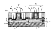
- FIG. 1 shows a substrate 1 comprising a film 2 made from first semiconductor material (designated here by reference numerals 2 a and 2 b ) on which a gate dielectric (not shown) and a gate electrode 3 have already been formed.
- Gate electrode 3 is separated from first semiconductor material film 2 by the gate dielectric.
- the source area 4 and drain area 5 can be formed in first semiconductor material film 2 and are separated by gate electrode 3 .
- Source and drain areas 4 and 5 are connected by a conduction channel formed in film 2 .
- the conduction channel is arranged under gate electrode 3 .
- Film 2 is monocrystalline. Film 2 is for example made from silicon, but it is also possible to use other semiconductor materials of valence IV or other suitable materials.
- the embodiment illustrated in FIG. 1 represents co-integration of two transistors T 1 and T 2 for which the first semiconducting materials are different and are noted 2 a and 2 b. As a variant, the two materials are identical.
- Substrate 1 can be a bulk substrate made from semiconductor material or a more complex substrate, for example a substrate of semiconductor on insulator type.
- substrate 1 successively comprises a film 2 made from first semiconductor material, an electrically insulating layer 6 and a support 7 which can be a second semiconductor film.
- Electrically insulating layer 6 can be formed by any suitable material, for example an oxide, a nitride, or a mixture of the latter.
- electrically insulating layer 6 can be made from silicon oxide or silicon nitride. It is particularly advantageous to use a substrate of semiconductor on insulator type and more particularly a substrate the thickness of the semiconductor film of which is smaller than or equal to 10 nm in order to have a high mechanical stress.
- the field-effect transistor can be a single transistor or several transistors can be formed on substrate 1 .
- an insulation pattern 8 for example a pattern made from electrically insulating material which sinks into the substrate also called isolation trench, in particular a trench referred to as STI standing for Shallow Trench Isolation.
- Source and/or drain areas 4 and 5 are formed from an electrically conducting material, preferably a doped semiconductor material. Different materials are used. Source and drain areas 4 and 5 can be formed from the same material as that forming the conduction channel as is illustrated for transistor T 2 . As a variant, it is also possible to form the source and drain areas from a material which has a different lattice parameter from the material forming the conduction channel in order to apply stress in the conduction channel as is illustrated for transistor T 1 . An opposite configuration can also be applied. In a particular embodiment, source and/or drain areas 4 and 5 are produced with a solid silicon/carbon solution. This material presents a lower lattice parameter than that of silicon which enables a set of tensile stresses to be applied on the conduction channel.
- transistors are integrated on the substrate, it is possible to have different materials from one transistor to the other, for example different materials for the nMOS transistors and the pMOS transistors.
- the thickness of source and drain areas 4 and 5 is comprised between 5 nm and 50 nm. In advantageous manner, the thickness of the source and drain areas is equal to or about 20 nm.
- the source and drain areas can be areas the apex of which is in the extension of the interface between first semiconductor material film 2 and the gate dielectric.
- source and drain areas 4 and 5 which are raised, i.e. an addition of material has been made for example to facilitate the subsequent silicidation step and advantageously to optimize the stresses in the conduction channel.
- source and drain areas etched in the semiconductor material film at a shallower level than the conduction channel.
- protection layer 9 (designated here by 9 a ′, 9 a ′′ and 9 b ) made in an electrically insulating material. Protection layer 9 covers gate electrode 3 and source and drain areas 4 and 5 . Protection layer 9 can be a compressive-stressed or tensile-stressed protection layer or a neutral layer.
- Protection layer 9 can be made from different types of silicon oxide, silicon nitride or another electrically insulating material.
- protection layer 9 it is advantageous to produce protection layer 9 with a stack of two different layers 9 a and 9 b.
- First protection layer 9 a is in contact with source and drain areas 4 and 5 and with gate electrode 3 .
- First protection layer 9 a is advantageously a layer which is stressed.
- Protection layer 9 a is a stressed layer which is in contact with transistor T 1 and which is specific to the transistor used.
- first protection layer 9 a ′ is in contact with transistor T 2 and is configured to apply a tensile stress on the channel of an nMOS transistor.
- first protection layer 9 a ′′ is in contact with the transistor and is configured to apply a compressive stress on the channel of a pMOS transistor.
- An opposite configuration for transistors T 1 and T 2 is also possible.
- First protection layer 9 a is covered by a second protection layer 9 b which can be neutral or which is less stressed.
- second layer 9 b is advantageously common to all the transistors.
- At least one hole is present in protection layer 9 to access source area 4 and/or drain area 5 .
- First and second protection layers 9 a and 9 b can be made from the same material, but it is advantageous to use two different materials in order to facilitate formation of an access hole to source area 4 , of an access hole to drain area 5 and of an access hole to gate electrode 3 .
- the use of two different materials enables the change of material when the etching step forming the access hole is performed to be better detected.
- first protection layer 9 a has a thickness comprised between 2 nm and 50 nm.
- protection layer 9 a is made from silicon nitride. It is advantageous to adjust the nitrogen content and the deposition conditions to form a compressive-stressed layer or a tensile-stressed layer.
- Second protection layer 9 b can have a thickness comprised between 2 nm and 150 nm.
- second protection layer 9 b is itself formed by two elementary layers (not shown).
- the first elementary layer of layer 9 b is a material able to flow and deposited by chemical vapor deposition, for example a silicon oxide.
- first protection layer 9 a is formed by a material which easily fills the holes, which is particularly advantageous for devices of small dimensions.
- the thickness of first protection layer 9 a is advantageously smaller than 50 nm.
- Second protection layer 9 b is for example a layer of TEOS (tetraethylorthosilicate) or a silicon oxide which can be deposited by High Density Plasma HDP, its thickness advantageously being less than 100 nm and advantageously more than 10 nm.
- TEOS tetraethylorthosilicate
- protection layer 9 presents an opening: it comprises an access hole to source area 4 and/or to drain area 5 .
- Protection layer 9 can cover the gate as is represented in FIG. 1 , but it is also possible to choose the thickness of the protection layer so as to come flush with the top part of the gate ( FIG. 6 ).
- protection layer 9 comprises an access hole to the source and drain areas and an access hole to the gate electrode.
- the access holes can be made by any suitable technique, for example by a photolithography step associated with an etching step.
- a hole can be made for each electrode ( FIG. 7 ) or it is possible to make one hole for the whole set of electrodes ( FIG. 8 ) and to use the lateral spacers of the gate electrode as electric insulator between the electrodes.
- An example embodiment of the access holes is illustrated in the documents US2013/0295734 and US 2013/0252412.
- the access holes can be of any shape.
- the smallest lateral dimension of the hole i.e. in a plane parallel to the surface of substrate 1 , is comprised between 5 and 30 nm.
- metallic material 10 is deposited in the access holes in order to form an interface between metallic material 10 and the semiconductor materials forming source area 4 , drain area 5 and possibly gate electrode 3 .
- Metallic material 10 can be deposited by any suitable technique, for example by chemical vapor deposition (CVD), by physical vapor deposition (PVD) or by electrochemical deposition.
- Metallic material 10 can be a pure element or a metal alloy, for example an alloy containing 90% Nickel and 10% Platinum (in atomic percentage).
- deposition of metallic material 10 is performed by a directional or selective deposition technique which enables the metallic material 10 to be localised in the bottom of the access holes and on the top of protection layer 9 .
- Deposition is advantageously performed in a direction perpendicular to the surface of the substrate, here perpendicular to the interface between the gate dielectric and the first semiconductor material.
- the use of directional or selective deposition enables deposition of the metallic material on the sides of the holes to be reduced or even prevented thereby preventing short-circuiting.
- the thickness of deposition of metallic material 10 and the annealing conditions are configured so as to define the quantity of semiconductor material and of metallic material which will react. According to the embodiments, it is possible to obtain partial or total reaction of the source and/or drain areas. It is also possible to provide for reaction of gate 3 . However, it is advantageous not to transform the channel.
- the deposited thickness of metallic material 10 is comprised between 0.5 nm and 10 nm and advantageously equal to 4 nm.
- annealing at 400° C. can be used to form a NiSi phase.
- Deposition of titanium or cobalt can also be formed and annealing at 600° C. can be used.
- two successive annealing at different temperatures are performed after filling the access hole. The first anneal is configured to form a first metal compound and the second anneal is configured to form a second metal compound different from the first metal compound.
- barrier layer 11 is for example made from TiN. Barrier layer 11 is an electrically conducting layer. Barrier layer 11 is made from a material which does not react with the semiconductor materials forming source and drain areas 4 and 5 or with the semiconductor material forming gate electrode 3 . Barrier layer 11 is made from a material which does not react with metallic material 10 .
- the barrier layer is advantageously a layer which blocks Cu, W and O atoms in order to obtain a device providing good electric performances. It is advantageous to form a conformal and continuous barrier layer.
- the barrier layer material is a more rigid material than semiconductor material 2 in order to limit deformation of barrier layer 11 during the fabrication method.
- Deposition of barrier layer 11 can be performed by means of a non-directional deposition technique or by means of another technique.
- the deposition performed is an isotropic deposition, i.e. it is performed using a technique which deposit the same thickness whatever the orientation of the surface to be covered.
- ALD atomic layer deposition
- MOCVD metalorganic chemical vapor deposition
- an anisotropic technique can also be used.
- barrier layer 11 is advantageously followed by deposition of an electric conductor 12 which will fill the access holes.
- This electric conductor 12 can be deposited by any suitable technique.
- This electric conductor 12 is for example tungsten or copper.
- the access hole can be completely filled by barrier layer 11 formed by a stack of several electrically conducting materials.
- the materials covering barrier layer 11 are metallic materials, for example pure metals or alloys.
- the Young's modulus of electric conductor 12 is higher than the Young's modulus of the semiconductor material to increase the stress transfer. For example, in the case where the semiconductor material is made from silicon (the Young's modulus is equal to 130 GPa), it is advantageous to use tungsten which has a Young's modulus equal to 406 GPa.
- the embodiment illustrated in FIG. 4 represents a co-integration of a transistor T 1 provided with an increased set of stresses and a transistor T 2 devoid of this increased set of stresses as there is no barrier layer 11 .
- barrier layer 11 is associated with deposition of electric conductor 12
- the thickness of barrier layer 11 is advantageously comprised between 1 and 10 nm.
- the thickness of electric conductor 12 is advantageously comprised between 1 and 25 nm. In advantageous manner, electric conductor 12 completely fills the hole, i.e. up to the top.
- deposition of metallic material 10 is followed by deposition of barrier layer 11 .
- This sequence is devoid of a low-temperature annealing step which leads to reaction of metallic material 10 with semiconductor material 2 in contact.
- This sequence is also devoid of a selective etching step of metallic material 10 which has not reacted with semiconductor material 2 .
- the deposition temperature of barrier layer 11 is therefore lower than the formation temperature of the alloy between metallic material 10 and semiconductor material 2 .
- the deposition temperature of electric conductor 12 is lower than the formation temperature of the metallic material coming from a semiconductor material 13 , e.g. silicide.
- the formation temperature of the alloy between the metallic material and the semiconductor material depends on the materials used.
- the following successive stack is to be found at the level of source area 4 and/or drain area 5 and possibly at the level of gate electrode 3 : semiconductor material 2 , non-reacted metallic material 10 and barrier layer 11 .
- heat treatment is performed and configured to make metallic material 10 react with the semiconductor material or materials after deposition of barrier layer 11 and preferably after filling of the access holes.
- the reaction for forming an alloy 13 between metallic material 10 and semiconductor material 2 is performed in a confined environment. Alloy 13 is electrically conducting.
- alloy 13 having a metallic behaviour based on semiconductor material and on a metal results in a reduction of volume.
- the volume occupied by alloy 13 is smaller than the volume initially occupied by metallic material 10 and semiconductor material 2 before reaction.
- the reaction takes place in solid state and in a confined environment, the reduction of volume leads to the appearance of a set of stresses on the conduction channel.
- the stress can be applied from source area 4 and/or from drain area 5 . It is particularly advantageous to perform formation of alloy 13 in source and drain areas 4 and 5 to have a maximum stress on the conduction channel.
- Silicidation of the semiconductor material forming gate electrode 3 has a relatively small effect on the mobility of the carriers. It is therefore possible to perform silicidation of the gate in a different manner from that which is used for source and drain electrodes 4 and 5 . It is also possible, later on in the method, to provide for replacement of the material delineating gate electrode 3 by a more suitable material.
- source and drain areas 4 and 5 are formed by silicon or by a material mainly containing silicon, it is advantageous to use a metallic material 10 chosen from titanium, palladium, platinum, cobalt, nickel, tantalum, molybdenum and tungsten and their alloys. In particularly advantageous manner, nickel and nickel alloys will be used as the difference of volume is large when formation of a silicide takes place.
- This fabrication method is particularly advantageous for formation of transistors of nMOS type as the stress applied is a tensile stress on the conduction channel. This effect can be associated with the use of source and drain areas 4 and 5 in a solid silicon/carbon solution.
- a step of localization of the different, notably metallic, materials in the access holes is performed before the heat treatment for formation of alloy 13 . Localisation is for example achieved by means of a chemical mechanical polishing step.
- transistors are formed and only a part of these transistors presents a tensile stress applied from the formation of alloy 13 .
- One way of performing co-integration is to protect certain transistors when deposition of the metals and metallic materials is performed in order to prevent generation of stresses from alloy 13 .
- a sacrificial material is deposited to cover and protect second transistor T 2 .
- First transistor T 1 is left uncovered.
- a first metal and at least one barrier layer are deposited. Heat treatment is performed so as to make the metallic material react with the semiconductor material. Then the sacrificial material is eliminated. The first transistor may be protected if required.
- a second metal is deposited and reacts with the semiconductor material to form a second field-effect transistor.
- the second metal can be identical or not to the first metal.
- barrier layer 11 it is also possible to deposit barrier layer 11 on several transistors and to eliminate this barrier layer where it is not desired, for example on transistor T 2 of FIG. 4 .
- second transistor T 2 it is possible to perform a more conventional transformation method by applying a first annealing configured to make the metallic material react with semiconductor material 2 forming source/drain areas 4 and 5 .
- the excess metallic material is then eliminated and a second annealing is performed so as to form the defined compound which presents the required electric characteristics.
- the first annealing will form an alloy substantially having the composition CoSi and the second annealing will form the alloy CoSi 2 .
- the annealing performed for formation of alloy 13 for transistor T 1 can be common with the annealing designed to form another alloy between a semiconductor material and a metallic material on transistor T 2 .
- the same metallic material is deposited for the two transistors.
- the metallic material is covered by barrier layer 11 for application of the stress.
- the barrier layer is absent. Under these conditions, when annealing is performed, the tensile stress is not applied as the volume of the alloy can change freely without generating a large quantity of stresses on the conduction channel.
- an oxygen blocking layer for example a thin layer of silicon nitride which will not be able to apply the stress on the source/drain areas of the transistor.
- transistor T 1 and transistor T 2 it may be easy to visually differentiate transistor T 1 and transistor T 2 .
- the metallic material is deposited by a physical vapor deposition technique, a part of the metallic material is present on the edges of the holes formed in protection layer 9 . This deposition is encapsulated by barrier layer 11 and it remains present throughout the method.
- the metallic material present on the sides of the holes does not react and is eliminated when removal of the metallic material which has not reacted is performed.
- This configuration is particularly advantageous as it is compatible with the use of stressed source and drain areas and it is also compatible with the use of stressed protection layers.
- a compressive stress may be present.
- the use of the method presented above enables this compressive stressed to be reduced. It is then advantageous to form two transistors one of which uses the barrier layer and the other of which is devoid of the barrier layer. In this case, it is possible to modulate the compressive stress in the transistor. For example, if the barrier layer presents a lower Young's modulus than that of the material forming conductor 12 , elimination of the barrier layer can result in an increase of the tensile strength. It will then be preferable to orient this embodiment preferentially to fabrication of nMOS transistors.
- a planarizing step is performed after deposition of protection layer 9 and more particularly after deposition of layer 9 b.
- the planarizing step is configured so that the surface of the stack is flat and that it comprises areas made from protection layer 9 and areas made from a gate pattern. In this manner, access to gate pattern 3 is ensured.
- the stack forming the gate pattern comprises an etch stop layer 14 for example made from silicon nitride.
- the surface comprises areas made from protection layer 9 and areas made from silicon nitride.
- Access to the source and/or drain areas can be achieved by means of a specific mask defining the contacts as illustrated in FIG. 7 .
- the mask comprises two cavities 15 a and 15 b which are designed to form two circular contact holes in protection layer 9 .
- a mask presenting a cavity 15 having the same shape as the active area or substantially the same shape as the active area to release a large surface of the source and drain areas.
- the mask is configured to access source area 4 and drain area 5 by means of a single cavity.
- the cavity extends on each side of gate electrode 3 .
- the cavity extends over the whole dimension of the active area, i.e. so as to reach insulation pattern 8 .
- the cavity of the mask advantageously extends along the other dimension to release the whole of the active area in the longitudinal axis of gate electrode 3 .
- the cavity of the mask can overlap onto the insulation pattern taking care not to short-circuit the source and drain areas. In the example illustrated in FIG. 8 , the cavity overlaps onto the insulation pattern in the direction perpendicular to the longitudinal axis of the gate electrode. Along the longitudinal axis of the gate electrode, the cavity does not extend up to the insulation pattern.
- a layer of metallic material 10 is deposited on the source and drain areas. Barrier layer 11 and then possibly electric conductor 12 are deposited. The annealing configured to form alloy 13 is performed.
Landscapes
- Engineering & Computer Science (AREA)
- Microelectronics & Electronic Packaging (AREA)
- Power Engineering (AREA)
- General Physics & Mathematics (AREA)
- Computer Hardware Design (AREA)
- Physics & Mathematics (AREA)
- Condensed Matter Physics & Semiconductors (AREA)
- Manufacturing & Machinery (AREA)
- Chemical & Material Sciences (AREA)
- Ceramic Engineering (AREA)
- Materials Engineering (AREA)
- Crystallography & Structural Chemistry (AREA)
- Insulated Gate Type Field-Effect Transistor (AREA)
Abstract
Description
-
- providing a substrate comprising:
- a film made from first semiconductor material,
- a gate dielectric covered by a gate electrode,
- source and drain areas separated by the gate electrode,
- a protection layer covering the gate electrode and the source and drain areas,
- an access hole to the source area and/or to the drain area,
- depositing a metallic material, in the access hole, in contact with the first semiconductor material of the source and/or drain area,
- providing a substrate comprising:
-
- depositing an electrically conducting barrier layer, the barrier layer being non-reactive with the first semiconductor material and non-reactive with the metallic material,
- performing a heat treatment so that the metallic material react with the semiconductor material to form an alloy of the metallic material and of the semiconductor material generating a set of stresses on a conduction channel arranged between the source and drain areas.
Claims (16)
Applications Claiming Priority (2)
| Application Number | Priority Date | Filing Date | Title |
|---|---|---|---|
| FR1400969 | 2014-04-24 | ||
| FR1400969A FR3020500B1 (en) | 2014-04-24 | 2014-04-24 | PROCESS FOR PRODUCING AN IMPROVED FIELD EFFECT TRANSISTOR |
Publications (2)
| Publication Number | Publication Date |
|---|---|
| US20150311287A1 US20150311287A1 (en) | 2015-10-29 |
| US9548210B2 true US9548210B2 (en) | 2017-01-17 |
Family
ID=50933261
Family Applications (1)
| Application Number | Title | Priority Date | Filing Date |
|---|---|---|---|
| US14/695,787 Active US9548210B2 (en) | 2014-04-24 | 2015-04-24 | Fabrication method of a transistor with improved field effect |
Country Status (2)
| Country | Link |
|---|---|
| US (1) | US9548210B2 (en) |
| FR (1) | FR3020500B1 (en) |
Cited By (1)
| Publication number | Priority date | Publication date | Assignee | Title |
|---|---|---|---|---|
| US10510886B2 (en) | 2017-10-26 | 2019-12-17 | Samsung Electronics Co., Ltd. | Method of providing reacted metal source-drain stressors for tensile channel stress |
Families Citing this family (3)
| Publication number | Priority date | Publication date | Assignee | Title |
|---|---|---|---|---|
| KR20200086922A (en) * | 2019-01-10 | 2020-07-20 | 삼성전자주식회사 | Semiconductor devices |
| FR3094562B1 (en) * | 2019-03-26 | 2021-09-03 | Commissariat Energie Atomique | Co-integration of contacts on different semiconductors |
| US11825661B2 (en) * | 2020-09-23 | 2023-11-21 | Taiwan Semiconductor Manufacturing Company Limited | Mobility enhancement by source and drain stress layer of implantation in thin film transistors |
Citations (11)
| Publication number | Priority date | Publication date | Assignee | Title |
|---|---|---|---|---|
| US5998873A (en) | 1998-12-16 | 1999-12-07 | National Semiconductor Corporation | Low contact resistance and low junction leakage metal interconnect contact structure |
| US20010016417A1 (en) | 1997-01-28 | 2001-08-23 | Micron Technology, Inc. | High pressure anneals of integrated circuit structures |
| US20060131662A1 (en) | 2004-12-17 | 2006-06-22 | Matsushita Electric Industrial Co., Ltd. | Semiconductor device |
| US20070269970A1 (en) | 2006-05-19 | 2007-11-22 | International Business Machines Corporation | Structure and method for forming cmos devices with intrinsically stressed silicide using silicon nitride cap |
| US20080157208A1 (en) | 2006-12-29 | 2008-07-03 | Fischer Kevin J | Stressed barrier plug slot contact structure for transistor performance enhancement |
| US20090152599A1 (en) | 2007-08-10 | 2009-06-18 | Semiconductor Manufacturing International (Shanghai) Corporation | Silicon Germanium and Polysilicon Gate Structure for Strained Silicon Transistors |
| US20120074502A1 (en) | 2010-09-28 | 2012-03-29 | International Business Machines Corporation | Use of contacts to create differential stresses on devices |
| US20130193577A1 (en) | 2012-02-01 | 2013-08-01 | I-Ming Tseng | Structure of electrical contact and fabrication method thereof |
| US20130252412A1 (en) | 2010-07-23 | 2013-09-26 | Commissariat A L' Energie Atomique Et Aux Energies Alternatives | Process for producing an integrated circuit |
| US20130295734A1 (en) | 2012-05-04 | 2013-11-07 | Commissariat A L'energie Atomique Et Aux Energies Alternatives | Method for forming gate, source, and drain contacts on a mos transistor |
| US20140154856A1 (en) * | 2012-12-05 | 2014-06-05 | International Business Machines Corporation | Inducing Channel Strain via Encapsulated Silicide Formation |
-
2014
- 2014-04-24 FR FR1400969A patent/FR3020500B1/en active Active
-
2015
- 2015-04-24 US US14/695,787 patent/US9548210B2/en active Active
Patent Citations (11)
| Publication number | Priority date | Publication date | Assignee | Title |
|---|---|---|---|---|
| US20010016417A1 (en) | 1997-01-28 | 2001-08-23 | Micron Technology, Inc. | High pressure anneals of integrated circuit structures |
| US5998873A (en) | 1998-12-16 | 1999-12-07 | National Semiconductor Corporation | Low contact resistance and low junction leakage metal interconnect contact structure |
| US20060131662A1 (en) | 2004-12-17 | 2006-06-22 | Matsushita Electric Industrial Co., Ltd. | Semiconductor device |
| US20070269970A1 (en) | 2006-05-19 | 2007-11-22 | International Business Machines Corporation | Structure and method for forming cmos devices with intrinsically stressed silicide using silicon nitride cap |
| US20080157208A1 (en) | 2006-12-29 | 2008-07-03 | Fischer Kevin J | Stressed barrier plug slot contact structure for transistor performance enhancement |
| US20090152599A1 (en) | 2007-08-10 | 2009-06-18 | Semiconductor Manufacturing International (Shanghai) Corporation | Silicon Germanium and Polysilicon Gate Structure for Strained Silicon Transistors |
| US20130252412A1 (en) | 2010-07-23 | 2013-09-26 | Commissariat A L' Energie Atomique Et Aux Energies Alternatives | Process for producing an integrated circuit |
| US20120074502A1 (en) | 2010-09-28 | 2012-03-29 | International Business Machines Corporation | Use of contacts to create differential stresses on devices |
| US20130193577A1 (en) | 2012-02-01 | 2013-08-01 | I-Ming Tseng | Structure of electrical contact and fabrication method thereof |
| US20130295734A1 (en) | 2012-05-04 | 2013-11-07 | Commissariat A L'energie Atomique Et Aux Energies Alternatives | Method for forming gate, source, and drain contacts on a mos transistor |
| US20140154856A1 (en) * | 2012-12-05 | 2014-06-05 | International Business Machines Corporation | Inducing Channel Strain via Encapsulated Silicide Formation |
Cited By (1)
| Publication number | Priority date | Publication date | Assignee | Title |
|---|---|---|---|---|
| US10510886B2 (en) | 2017-10-26 | 2019-12-17 | Samsung Electronics Co., Ltd. | Method of providing reacted metal source-drain stressors for tensile channel stress |
Also Published As
| Publication number | Publication date |
|---|---|
| US20150311287A1 (en) | 2015-10-29 |
| FR3020500B1 (en) | 2017-09-01 |
| FR3020500A1 (en) | 2015-10-30 |
Similar Documents
| Publication | Publication Date | Title |
|---|---|---|
| US10043885B2 (en) | Bi-layer metal deposition in silicide formation | |
| US10297511B2 (en) | Fin-FET device and fabrication method thereof | |
| CN104867967B (en) | Semiconductor devices and its manufacture method | |
| US9496283B1 (en) | Transistor with self-aligned source and drain contacts and method of making same | |
| US9553189B2 (en) | Self-aligned silicide formation on source/drain through contact via | |
| US10573749B2 (en) | Fin-type field effect transistor structure and manufacturing method thereof | |
| CN108231588A (en) | Transistor and forming method thereof | |
| US8796099B2 (en) | Inducing channel strain via encapsulated silicide formation | |
| TWI685974B (en) | Fin-type field effect transistor device and manufacturing method thereof | |
| US9548210B2 (en) | Fabrication method of a transistor with improved field effect | |
| US9368627B2 (en) | Semiconductor structure and manufacturing method thereof | |
| TWI715674B (en) | Fin-type field effect transistor device and manufacturing method thereof | |
| US11335681B2 (en) | Fin-type field effect transistor structure and manufacturing method thereof | |
| CN106531686A (en) | Interconnection structure, fabricating method thereof, and semiconductor device using the same | |
| KR20170065271A (en) | A semiconductor device and methods of manufacturing the same | |
| US20170033217A1 (en) | Semiconductor devices and methods of manufacturing the same | |
| US9893184B2 (en) | Fin-type field effect transistor device and method of fabricating the same | |
| EP3032575B1 (en) | Method for forming an electrical contact. | |
| US20170047422A1 (en) | Semiconductor device and a fabrication method thereof | |
| JP5286416B2 (en) | Semiconductor device and manufacturing method thereof | |
| TW201330253A (en) | MOSFET integrated circuit with improved silicide thickness uniformity and methods for its manufacture | |
| TWI770748B (en) | Semiconductor devices and methods for manufacturing the same | |
| US20220262925A1 (en) | Nano-Fet Semiconductor Device and Method of Forming | |
| KR102501422B1 (en) | Semiconductor device and manufacturing method thereof | |
| US9806169B2 (en) | Semiconductor devices having a gate stack |
Legal Events
| Date | Code | Title | Description |
|---|---|---|---|
| AS | Assignment |
Owner name: COMMISSARIAT A L'ENERGIE ATOMIQUE ET AUX ENERGIES Free format text: ASSIGNMENT OF ASSIGNORS INTEREST;ASSIGNORS:NEMOUCHI, FABRICE;BOURJOT, EMILIE;REEL/FRAME:035492/0350 Effective date: 20150417 Owner name: STMICROELECTRONICS (CROLLES 2) SAS, FRANCE Free format text: ASSIGNMENT OF ASSIGNORS INTEREST;ASSIGNORS:NEMOUCHI, FABRICE;BOURJOT, EMILIE;REEL/FRAME:035492/0350 Effective date: 20150417 |
|
| STCF | Information on status: patent grant |
Free format text: PATENTED CASE |
|
| CC | Certificate of correction | ||
| MAFP | Maintenance fee payment |
Free format text: PAYMENT OF MAINTENANCE FEE, 4TH YEAR, LARGE ENTITY (ORIGINAL EVENT CODE: M1551); ENTITY STATUS OF PATENT OWNER: LARGE ENTITY Year of fee payment: 4 |