US9543528B2 - Compound for an organic optoelectric device, organic optoelectric device including the same, and display device including the optoelectric device - Google Patents
Compound for an organic optoelectric device, organic optoelectric device including the same, and display device including the optoelectric device Download PDFInfo
- Publication number
- US9543528B2 US9543528B2 US14/283,935 US201414283935A US9543528B2 US 9543528 B2 US9543528 B2 US 9543528B2 US 201414283935 A US201414283935 A US 201414283935A US 9543528 B2 US9543528 B2 US 9543528B2
- Authority
- US
- United States
- Prior art keywords
- group
- substituted
- unsubstituted
- compound
- chemical formula
- Prior art date
- Legal status (The legal status is an assumption and is not a legal conclusion. Google has not performed a legal analysis and makes no representation as to the accuracy of the status listed.)
- Active, expires
Links
- 0 *1c(c(c2cccc3c22)c(cc4)[n]2-c(cccc2)c2N3c2nc(-c3ccccc3)cc(-c3ccccc3)n2)c4-c2c1cccc2 Chemical compound *1c(c(c2cccc3c22)c(cc4)[n]2-c(cccc2)c2N3c2nc(-c3ccccc3)cc(-c3ccccc3)n2)c4-c2c1cccc2 0.000 description 42
- BKHYTNZJPJKCDX-UHFFFAOYSA-N C1=CC=C(C2=CC(C3=CC=CC=C3)=CC(N3C4=CC=CC=C4N4C5=C(C=C6C(=C5)N(C5=CC=CC=C5)C5=C6C=CC=C5)C5=C4/C3=C\C=C/5)=C2)C=C1.C1=CC=C(C2=CC(C3=CC=CC=C3)=CC(N3C4=CC=CC=C4N4C5=C(C=CC6=C5C5=C(C=CC=C5)N6C5=CC=CC=C5)C5=C4/C3=C\C=C/5)=C2)C=C1.C1=CC=C(C2=CC(C3=CC=CC=C3)=CC(N3C4=CC=CC=C4N4C5=C(C=CC6=C5N(C5=CC=CC=C5)C5=C6C=CC=C5)C5=C4/C3=C\C=C/5)=C2)C=C1.C1=CC=C(N2C3=CC=CC=C3N3C4=C(C5=C3/C2=C\C=C/5)C2=C(C=C4)N(C3=CC=CC(C4=CN=CC=C4)=C3)C3=C2C=CC=C3)C=C1 Chemical compound C1=CC=C(C2=CC(C3=CC=CC=C3)=CC(N3C4=CC=CC=C4N4C5=C(C=C6C(=C5)N(C5=CC=CC=C5)C5=C6C=CC=C5)C5=C4/C3=C\C=C/5)=C2)C=C1.C1=CC=C(C2=CC(C3=CC=CC=C3)=CC(N3C4=CC=CC=C4N4C5=C(C=CC6=C5C5=C(C=CC=C5)N6C5=CC=CC=C5)C5=C4/C3=C\C=C/5)=C2)C=C1.C1=CC=C(C2=CC(C3=CC=CC=C3)=CC(N3C4=CC=CC=C4N4C5=C(C=CC6=C5N(C5=CC=CC=C5)C5=C6C=CC=C5)C5=C4/C3=C\C=C/5)=C2)C=C1.C1=CC=C(N2C3=CC=CC=C3N3C4=C(C5=C3/C2=C\C=C/5)C2=C(C=C4)N(C3=CC=CC(C4=CN=CC=C4)=C3)C3=C2C=CC=C3)C=C1 BKHYTNZJPJKCDX-UHFFFAOYSA-N 0.000 description 2
- QPKSVKHJFJMKRR-UHFFFAOYSA-N C1=CC=C2C(=C1)N1C3=C(C4=C1/C(=C\C=C/4)N2C1=CC2=C(C=C1)SC1=C2C=CC=C1)C1=C(C=C3)C2=C(C=CC=C2)O1.C1=CC=C2C(=C1)N1C3=C(C4=C1/C(=C\C=C/4)N2C1=CC2=C(C=C1)SC1=C2C=CC=C1)C1=C(C=C3)C2=C(C=CC=C2)S1.C1=CC=C2C(=C1)N1C3=C(C4=C1/C(=C\C=C/4)N2C1=CC2=C(C=C1)SC1=C2C=CC=C1)C1=C(C=C3)OC2=C1C=CC=C2.C1=CC=C2C(=C1)N1C3=C(C4=C1/C(=C\C=C/4)N2C1=CC2=C(C=C1)SC1=C2C=CC=C1)C1=C(C=C3)SC2=C1C=CC=C2 Chemical compound C1=CC=C2C(=C1)N1C3=C(C4=C1/C(=C\C=C/4)N2C1=CC2=C(C=C1)SC1=C2C=CC=C1)C1=C(C=C3)C2=C(C=CC=C2)O1.C1=CC=C2C(=C1)N1C3=C(C4=C1/C(=C\C=C/4)N2C1=CC2=C(C=C1)SC1=C2C=CC=C1)C1=C(C=C3)C2=C(C=CC=C2)S1.C1=CC=C2C(=C1)N1C3=C(C4=C1/C(=C\C=C/4)N2C1=CC2=C(C=C1)SC1=C2C=CC=C1)C1=C(C=C3)OC2=C1C=CC=C2.C1=CC=C2C(=C1)N1C3=C(C4=C1/C(=C\C=C/4)N2C1=CC2=C(C=C1)SC1=C2C=CC=C1)C1=C(C=C3)SC2=C1C=CC=C2 QPKSVKHJFJMKRR-UHFFFAOYSA-N 0.000 description 2
- GWYBTZVYJDWPBE-UHFFFAOYSA-N C1=CC=C2C(=C1)N1C3=C(C=C4C(=C3)OC3=C4C=CC=C3)C3=C1/C(=C\C=C/3)N2C1=CC2=C(C=C1)SC1=C2C=CC=C1.C1=CC=C2C(=C1)N1C3=C(C=C4C(=C3)SC3=C4C=CC=C3)C3=C1/C(=C\C=C/3)N2C1=CC2=C(C=C1)SC1=C2C=CC=C1.C1=CC=C2C(=C1)N1C3=C(C=C4OC5=C(C=CC=C5)C4=C3)C3=C1/C(=C\C=C/3)N2C1=CC2=C(C=C1)SC1=C2C=CC=C1.C1=CC=C2C(=C1)N1C3=C(C=C4SC5=C(C=CC=C5)C4=C3)C3=C1/C(=C\C=C/3)N2C1=CC2=C(C=C1)SC1=C2C=CC=C1 Chemical compound C1=CC=C2C(=C1)N1C3=C(C=C4C(=C3)OC3=C4C=CC=C3)C3=C1/C(=C\C=C/3)N2C1=CC2=C(C=C1)SC1=C2C=CC=C1.C1=CC=C2C(=C1)N1C3=C(C=C4C(=C3)SC3=C4C=CC=C3)C3=C1/C(=C\C=C/3)N2C1=CC2=C(C=C1)SC1=C2C=CC=C1.C1=CC=C2C(=C1)N1C3=C(C=C4OC5=C(C=CC=C5)C4=C3)C3=C1/C(=C\C=C/3)N2C1=CC2=C(C=C1)SC1=C2C=CC=C1.C1=CC=C2C(=C1)N1C3=C(C=C4SC5=C(C=CC=C5)C4=C3)C3=C1/C(=C\C=C/3)N2C1=CC2=C(C=C1)SC1=C2C=CC=C1 GWYBTZVYJDWPBE-UHFFFAOYSA-N 0.000 description 2
- RIPSGVOVSHKUIK-UHFFFAOYSA-N C1=CC=C2C(=C1)N1C3=C(C=CC4=C3C3=C(C=CC=C3)O4)C3=C1/C(=C\C=C/3)N2C1=CC2=C(C=C1)SC1=C2C=CC=C1.C1=CC=C2C(=C1)N1C3=C(C=CC4=C3C3=C(C=CC=C3)S4)C3=C1/C(=C\C=C/3)N2C1=CC2=C(C=C1)SC1=C2C=CC=C1.C1=CC=C2C(=C1)N1C3=C(C=CC4=C3OC3=C4C=CC=C3)C3=C1/C(=C\C=C/3)N2C1=CC2=C(C=C1)SC1=C2C=CC=C1.C1=CC=C2C(=C1)N1C3=C(C=CC4=C3SC3=C4C=CC=C3)C3=C1/C(=C\C=C/3)N2C1=CC2=C(C=C1)SC1=C2C=CC=C1.C1=CC=C2C(=C1)OC1=C2C=CC=C1N1C2=CC=CC=C2N2C3=C(C4=C2/C1=C\C=C/4)C1=C(C=C3)OC2=C1C=CC=C2 Chemical compound C1=CC=C2C(=C1)N1C3=C(C=CC4=C3C3=C(C=CC=C3)O4)C3=C1/C(=C\C=C/3)N2C1=CC2=C(C=C1)SC1=C2C=CC=C1.C1=CC=C2C(=C1)N1C3=C(C=CC4=C3C3=C(C=CC=C3)S4)C3=C1/C(=C\C=C/3)N2C1=CC2=C(C=C1)SC1=C2C=CC=C1.C1=CC=C2C(=C1)N1C3=C(C=CC4=C3OC3=C4C=CC=C3)C3=C1/C(=C\C=C/3)N2C1=CC2=C(C=C1)SC1=C2C=CC=C1.C1=CC=C2C(=C1)N1C3=C(C=CC4=C3SC3=C4C=CC=C3)C3=C1/C(=C\C=C/3)N2C1=CC2=C(C=C1)SC1=C2C=CC=C1.C1=CC=C2C(=C1)OC1=C2C=CC=C1N1C2=CC=CC=C2N2C3=C(C4=C2/C1=C\C=C/4)C1=C(C=C3)OC2=C1C=CC=C2 RIPSGVOVSHKUIK-UHFFFAOYSA-N 0.000 description 2
- ITXCQFIKZMKJDD-UHFFFAOYSA-N C1=CC=C2C(=C1)OC1=C2C=CC=C1N1C2=CC=CC=C2N2C3=C(C4=C2/C1=C\C=C/4)C1=C(C=C3)C2=C(C=CC=C2)O1.C1=CC=C2C(=C1)OC1=C2C=CC=C1N1C2=CC=CC=C2N2C3=C(C4=C2/C1=C\C=C/4)C1=C(C=C3)C2=C(C=CC=C2)S1.C1=CC=C2C(=C1)OC1=C2C=CC=C1N1C2=CC=CC=C2N2C3=C(C4=C2/C1=C\C=C/4)C1=C(C=C3)SC2=C1C=CC=C2 Chemical compound C1=CC=C2C(=C1)OC1=C2C=CC=C1N1C2=CC=CC=C2N2C3=C(C4=C2/C1=C\C=C/4)C1=C(C=C3)C2=C(C=CC=C2)O1.C1=CC=C2C(=C1)OC1=C2C=CC=C1N1C2=CC=CC=C2N2C3=C(C4=C2/C1=C\C=C/4)C1=C(C=C3)C2=C(C=CC=C2)S1.C1=CC=C2C(=C1)OC1=C2C=CC=C1N1C2=CC=CC=C2N2C3=C(C4=C2/C1=C\C=C/4)C1=C(C=C3)SC2=C1C=CC=C2 ITXCQFIKZMKJDD-UHFFFAOYSA-N 0.000 description 2
- WYVKZXKEHXDFLF-UHFFFAOYSA-N c(cc1)cc(c2c34)c1[o]c2ccc3[n]1-c2ccccc2N(c(cc2)ccc2-c2cnccc2)c2c1c4ccc2 Chemical compound c(cc1)cc(c2c34)c1[o]c2ccc3[n]1-c2ccccc2N(c(cc2)ccc2-c2cnccc2)c2c1c4ccc2 WYVKZXKEHXDFLF-UHFFFAOYSA-N 0.000 description 2
- WDEBOLRRLTVLMH-UHFFFAOYSA-N c(cc1)cc(c2c34)c1[s]c2ccc3[n]1-c(cccc2)c2N(c(cc2)ccc2-c2ccncc2)c2c1c4ccc2 Chemical compound c(cc1)cc(c2c34)c1[s]c2ccc3[n]1-c(cccc2)c2N(c(cc2)ccc2-c2ccncc2)c2c1c4ccc2 WDEBOLRRLTVLMH-UHFFFAOYSA-N 0.000 description 2
- POWBQTGIHFDZBX-UHFFFAOYSA-N c(cc1)ccc1-[n](c(cccc1)c1c1c2c3cccc4c33)c1ccc2[n]3-c1ccccc1N4c1cccc2c1[o]c1ccccc21 Chemical compound c(cc1)ccc1-[n](c(cccc1)c1c1c2c3cccc4c33)c1ccc2[n]3-c1ccccc1N4c1cccc2c1[o]c1ccccc21 POWBQTGIHFDZBX-UHFFFAOYSA-N 0.000 description 2
- ODCVIQJWGQPOMA-UHFFFAOYSA-N c(cc1)ccc1-[n](c1ccccc1c1c2)c1cc(c1cccc3c11)c2[n]1-c1ccccc1N3c1cccc2c1[o]c1ccccc21 Chemical compound c(cc1)ccc1-[n](c1ccccc1c1c2)c1cc(c1cccc3c11)c2[n]1-c1ccccc1N3c1cccc2c1[o]c1ccccc21 ODCVIQJWGQPOMA-UHFFFAOYSA-N 0.000 description 2
- OOYXKHHLURWRDA-UHFFFAOYSA-N c(cc1)ccc1-[n]1c(c(c2cccc3c22)c(cc4)[n]2-c2ccccc2N3c2cccc3c2[o]c2ccccc32)c4c2ccccc12 Chemical compound c(cc1)ccc1-[n]1c(c(c2cccc3c22)c(cc4)[n]2-c2ccccc2N3c2cccc3c2[o]c2ccccc32)c4c2ccccc12 OOYXKHHLURWRDA-UHFFFAOYSA-N 0.000 description 2
- HMLHHPPHFDOKMK-UHFFFAOYSA-N c(cc1)ccc1-[n]1c(cc(c(c2cccc3c22)c4)[n]2-c2ccccc2N3c2cccc3c2[o]c2ccccc32)c4c2ccccc12 Chemical compound c(cc1)ccc1-[n]1c(cc(c(c2cccc3c22)c4)[n]2-c2ccccc2N3c2cccc3c2[o]c2ccccc32)c4c2ccccc12 HMLHHPPHFDOKMK-UHFFFAOYSA-N 0.000 description 2
- BDXWDOUJHNGBBZ-UHFFFAOYSA-N c(cc12)ccc1[o]c(cc1)c2c2c1c1cccc3c1[n]2-c(cccc1)c1N3c(cc1)ccc1-c1cnccc1 Chemical compound c(cc12)ccc1[o]c(cc1)c2c2c1c1cccc3c1[n]2-c(cccc1)c1N3c(cc1)ccc1-c1cnccc1 BDXWDOUJHNGBBZ-UHFFFAOYSA-N 0.000 description 2
- ZLGWMYXMKAQOLI-UHFFFAOYSA-N c(cc12)ccc1[s]c(cc1)c2c2c1c1cccc3c1[n]2-c(cccc1)c1N3c(cc1)ccc1-c1cnccc1 Chemical compound c(cc12)ccc1[s]c(cc1)c2c2c1c1cccc3c1[n]2-c(cccc1)c1N3c(cc1)ccc1-c1cnccc1 ZLGWMYXMKAQOLI-UHFFFAOYSA-N 0.000 description 2
- BYDDORKACHYZBZ-UHFFFAOYSA-N c(cc1c2c3)ccc1[o]c2cc1c3c2cccc3c2[n]1-c1ccccc1N3c(cc1)ccc1-c1cnccc1 Chemical compound c(cc1c2c3)ccc1[o]c2cc1c3c2cccc3c2[n]1-c1ccccc1N3c(cc1)ccc1-c1cnccc1 BYDDORKACHYZBZ-UHFFFAOYSA-N 0.000 description 2
- BFHGWINKCRNPFR-UHFFFAOYSA-N c1ccc2[o]c(c3c(cc4)c5cccc6c5[n]3-c(cccc3)c3N6c(cc3)ccc3-c3cnccc3)c4c2c1 Chemical compound c1ccc2[o]c(c3c(cc4)c5cccc6c5[n]3-c(cccc3)c3N6c(cc3)ccc3-c3cnccc3)c4c2c1 BFHGWINKCRNPFR-UHFFFAOYSA-N 0.000 description 2
- KRGSAWINUXILOY-UHFFFAOYSA-N c1ccc2[s]c(cc(c3c4)[n]5-c(cccc6)c6N(c(cc6)ccc6-c6cnccc6)c6c5c3ccc6)c4c2c1 Chemical compound c1ccc2[s]c(cc(c3c4)[n]5-c(cccc6)c6N(c(cc6)ccc6-c6cnccc6)c6c5c3ccc6)c4c2c1 KRGSAWINUXILOY-UHFFFAOYSA-N 0.000 description 2
- DDJCIOKEBBOAPC-UHFFFAOYSA-N *.B.BrC1=C2C(=CC=C1)C1=C(C=CC=C1)N2C1=CC=CC=C1.BrC1=C2CC3=C(C=CC=C3)C2=CC=C1.C1=CC=C(C2=NC(C3=CC=CC=C3)=NC(N3C4=C(C=CC=C4)N4C5=C(C=CC6=C5N(C5=CC=CC=C5)C5=C6C=CC=C5)C5=CC=CC3=C54)=N2)C=C1.IC1=CC=CC=C1 Chemical compound *.B.BrC1=C2C(=CC=C1)C1=C(C=CC=C1)N2C1=CC=CC=C1.BrC1=C2CC3=C(C=CC=C3)C2=CC=C1.C1=CC=C(C2=NC(C3=CC=CC=C3)=NC(N3C4=C(C=CC=C4)N4C5=C(C=CC6=C5N(C5=CC=CC=C5)C5=C6C=CC=C5)C5=CC=CC3=C54)=N2)C=C1.IC1=CC=CC=C1 DDJCIOKEBBOAPC-UHFFFAOYSA-N 0.000 description 1
- UKKRAFPETUKUAH-RKKUYXDDSA-N *.B.BrC1=C2OC3=C(C=CC=C3)C2=CC=C1.BrC1=NC(C2=CC=CC=C2)=NC(C2=CC=CC=C2)=N1.C.C.C1=CC2=C(C=C1)C1=CC=C3C4=C(C=CC=C4)OC3=C1N2.C1=CC=C(C2=NC(C3=CC=CC=C3)=NC(N3C4=CC=CC=C4N4C5=C(C=CC=C53)C3=CC=C5C6=C(C=CC=C6)OC5=C34)=N2)C=C1.C1=CC=C2C(=C1)CC1=CC=CC3=C1N2C1=C2OC4=C(C=CC=C4)C2=CC=C31.ClC1=CC=CC=C1NC1=C2OC3=C(C=CC=C3)C2=CC=C1.F.NC1=CC=CC=C1Cl.O=[N+]([O-])C1=CC=CC=C1Br.O=[N+]([O-])C1=CC=CC=C1N1C2=C(C=CC=C2)C2=CC=C3C4=C(C=CC=C4)OC3=C21.[2HH] Chemical compound *.B.BrC1=C2OC3=C(C=CC=C3)C2=CC=C1.BrC1=NC(C2=CC=CC=C2)=NC(C2=CC=CC=C2)=N1.C.C.C1=CC2=C(C=C1)C1=CC=C3C4=C(C=CC=C4)OC3=C1N2.C1=CC=C(C2=NC(C3=CC=CC=C3)=NC(N3C4=CC=CC=C4N4C5=C(C=CC=C53)C3=CC=C5C6=C(C=CC=C6)OC5=C34)=N2)C=C1.C1=CC=C2C(=C1)CC1=CC=CC3=C1N2C1=C2OC4=C(C=CC=C4)C2=CC=C31.ClC1=CC=CC=C1NC1=C2OC3=C(C=CC=C3)C2=CC=C1.F.NC1=CC=CC=C1Cl.O=[N+]([O-])C1=CC=CC=C1Br.O=[N+]([O-])C1=CC=CC=C1N1C2=C(C=CC=C2)C2=CC=C3C4=C(C=CC=C4)OC3=C21.[2HH] UKKRAFPETUKUAH-RKKUYXDDSA-N 0.000 description 1
- VBYFRLCMELWFLF-HHVZCZSDSA-M *.B.BrC1=CC2=C(C=C1)CC1=CC=CC=C12.BrC1=CC=C2C(=C1)C1=C(C=CC=C1)N2C1=NC(C2=CC=CC=C2)=NC(C2=CC=CC=C2)=N1.C.C1=CC=C(C2=NC(C3=CC=CC=C3)=NC(N3C4=CC5=C(C=C4C4=C3C=CC=C4)N3C4=C(C=CC=C4)NC4=C3/C5=C\C=C/4)=N2)C=C1.ClC1=NC(C2=CC=CC=C2)=NC(C2=CC=CC=C2)=N1.O=COO[K].[2H]CF.[KH] Chemical compound *.B.BrC1=CC2=C(C=C1)CC1=CC=CC=C12.BrC1=CC=C2C(=C1)C1=C(C=CC=C1)N2C1=NC(C2=CC=CC=C2)=NC(C2=CC=CC=C2)=N1.C.C1=CC=C(C2=NC(C3=CC=CC=C3)=NC(N3C4=CC5=C(C=C4C4=C3C=CC=C4)N3C4=C(C=CC=C4)NC4=C3/C5=C\C=C/4)=N2)C=C1.ClC1=NC(C2=CC=CC=C2)=NC(C2=CC=CC=C2)=N1.O=COO[K].[2H]CF.[KH] VBYFRLCMELWFLF-HHVZCZSDSA-M 0.000 description 1
- YZPCYFJXLKGEAQ-UHFFFAOYSA-N BrC1=CC=CC2=C1C1=CC=CC=C1C2.C1=CC=C(C2=NC(C3=CC=CC=C3)=NC(N3C4=C(C=CC=C4)N4C5=C(C=CC6=C5C5=C(C=CC=C5)N6C5=CC=CC=C5)C5=CC=CC3=C54)=N2)C=C1 Chemical compound BrC1=CC=CC2=C1C1=CC=CC=C1C2.C1=CC=C(C2=NC(C3=CC=CC=C3)=NC(N3C4=C(C=CC=C4)N4C5=C(C=CC6=C5C5=C(C=CC=C5)N6C5=CC=CC=C5)C5=CC=CC3=C54)=N2)C=C1 YZPCYFJXLKGEAQ-UHFFFAOYSA-N 0.000 description 1
- RGVNRPRHVOASIZ-UHFFFAOYSA-N C(C(C=C1)[n]2c(c3c(cc4)[n]5-c(cccc6)c6N(c6ccccc6)c6c5c3ccc6)c4c3c2cccc3)c2c1[s]c1c2cccc1 Chemical compound C(C(C=C1)[n]2c(c3c(cc4)[n]5-c(cccc6)c6N(c6ccccc6)c6c5c3ccc6)c4c3c2cccc3)c2c1[s]c1c2cccc1 RGVNRPRHVOASIZ-UHFFFAOYSA-N 0.000 description 1
- SJECDFDVKGMBBR-UHFFFAOYSA-N C.C.C.C.C.C1=CC=C(N2C3=CC=CC=C3N3C4=C(C5=C3/C2=C\C=C/5)C2=C(C=C4)N(C3=CC=C(N4C5=C(C=CC=C5)C5=C4C=CC=C5)C=C3)C3=C2C=CC=C3)C=C1.C1=CC=C(N2C3=CC=CC=C3N3C4=C(C=CC5=C4C4=C(C=CC=C4)O5)C4=C3/C2=C\C=C/4)C=C1.C1=CC=C(N2C3=CC=CC=C3N3C4=C(C=CC5=C4C4=C(C=CC=C4)S5)C4=C3/C2=C\C=C/4)C=C1.C1=CC=C(N2C3=CC=CC=C3N3C4=C(C=CC5=C4OC4=C5C=CC=C4)C4=C3/C2=C\C=C/4)C=C1.C1=CC=C(N2C3=CC=CC=C3N3C4=C(C=CC5=C4SC4=C5C=CC=C4)C4=C3/C2=C\C=C/4)C=C1 Chemical compound C.C.C.C.C.C1=CC=C(N2C3=CC=CC=C3N3C4=C(C5=C3/C2=C\C=C/5)C2=C(C=C4)N(C3=CC=C(N4C5=C(C=CC=C5)C5=C4C=CC=C5)C=C3)C3=C2C=CC=C3)C=C1.C1=CC=C(N2C3=CC=CC=C3N3C4=C(C=CC5=C4C4=C(C=CC=C4)O5)C4=C3/C2=C\C=C/4)C=C1.C1=CC=C(N2C3=CC=CC=C3N3C4=C(C=CC5=C4C4=C(C=CC=C4)S5)C4=C3/C2=C\C=C/4)C=C1.C1=CC=C(N2C3=CC=CC=C3N3C4=C(C=CC5=C4OC4=C5C=CC=C4)C4=C3/C2=C\C=C/4)C=C1.C1=CC=C(N2C3=CC=CC=C3N3C4=C(C=CC5=C4SC4=C5C=CC=C4)C4=C3/C2=C\C=C/4)C=C1 SJECDFDVKGMBBR-UHFFFAOYSA-N 0.000 description 1
- DDTDIFRZHARAHW-UHFFFAOYSA-N C.C.C1=CC=C(N2C3=CC=CC=C3N3C4=C(C5=C3/C2=C\C=C/5)C2=C(C=C4)C3=C(C=CC=C3)N2C2=CC=C(N3C4=C(C=CC=C4)C4=C3C=CC=C4)C=C2)C=C1.C1=CC=C(N2C3=CC=CC=C3N3C4=C(C=C5C(=C4)C4=C(C=CC=C4)N5C4=CC=C(N5C6=C(C=CC=C6)C6=C5C=CC=C6)C=C4)C4=C3/C2=C\C=C/4)C=C1 Chemical compound C.C.C1=CC=C(N2C3=CC=CC=C3N3C4=C(C5=C3/C2=C\C=C/5)C2=C(C=C4)C3=C(C=CC=C3)N2C2=CC=C(N3C4=C(C=CC=C4)C4=C3C=CC=C4)C=C2)C=C1.C1=CC=C(N2C3=CC=CC=C3N3C4=C(C=C5C(=C4)C4=C(C=CC=C4)N5C4=CC=C(N5C6=C(C=CC=C6)C6=C5C=CC=C6)C=C4)C4=C3/C2=C\C=C/4)C=C1 DDTDIFRZHARAHW-UHFFFAOYSA-N 0.000 description 1
- AJIIIOBOMGQURV-UHFFFAOYSA-N C.C1=CC=C(N2C3=CC=CC=C3N3C4=C(C5=C3/C2=C\C=C/5)C2=C(C=C4)C3=C(C=CC=C3)N2C2=CC=C(C3=CC=CN=C3)C=C2)C=C1.C1=CC=C(N2C3=CC=CC=C3N3C4=C(C=C5C(=C4)C4=C(C=CC=C4)N5C4=CC=C(C5=CC=CN=C5)C=C4)C4=C3/C2=C\C=C/4)C=C1.C1=CC=C(N2C3=CC=CC=C3N3C4=C(C=C5C(=C4)N(C4=CC=C(C6=CC=CN=C6)C=C4)C4=C5C=CC=C4)C4=C3/C2=C\C=C/4)C=C1.C1=CC=C(N2C3=CC=CC=C3N3C4=C(C=CC5=C4C4=C(C=CC=C4)N5C4=CC=C(C5=CC=CN=C5)C=C4)C4=C3/C2=C\C=C/4)C=C1 Chemical compound C.C1=CC=C(N2C3=CC=CC=C3N3C4=C(C5=C3/C2=C\C=C/5)C2=C(C=C4)C3=C(C=CC=C3)N2C2=CC=C(C3=CC=CN=C3)C=C2)C=C1.C1=CC=C(N2C3=CC=CC=C3N3C4=C(C=C5C(=C4)C4=C(C=CC=C4)N5C4=CC=C(C5=CC=CN=C5)C=C4)C4=C3/C2=C\C=C/4)C=C1.C1=CC=C(N2C3=CC=CC=C3N3C4=C(C=C5C(=C4)N(C4=CC=C(C6=CC=CN=C6)C=C4)C4=C5C=CC=C4)C4=C3/C2=C\C=C/4)C=C1.C1=CC=C(N2C3=CC=CC=C3N3C4=C(C=CC5=C4C4=C(C=CC=C4)N5C4=CC=C(C5=CC=CN=C5)C=C4)C4=C3/C2=C\C=C/4)C=C1 AJIIIOBOMGQURV-UHFFFAOYSA-N 0.000 description 1
- YXIJJEPVAWEYMD-UHFFFAOYSA-N C.C1=CC=C(N2C3=CC=CC=C3N3C4=C(C5=C3/C2=C\C=C/5)C2=C(C=C4)C3=C(C=CC=C3)S2)C=C1.C1=CC=C(N2C3=CC=CC=C3N3C4=C(C=C5C(=C4)OC4=C5C=CC=C4)C4=C3/C2=C\C=C/4)C=C1.C1=CC=C(N2C3=CC=CC=C3N3C4=C(C=C5C(=C4)SC4=C5C=CC=C4)C4=C3/C2=C\C=C/4)C=C1.C1=CC=C(N2C3=CC=CC=C3N3C4=C(C=C5OC6=C(C=CC=C6)C5=C4)C4=C3/C2=C\C=C/4)C=C1.C1=CC=C(N2C3=CC=CC=C3N3C4=C(C=C5SC6=C(C=CC=C6)C5=C4)C4=C3/C2=C\C=C/4)C=C1 Chemical compound C.C1=CC=C(N2C3=CC=CC=C3N3C4=C(C5=C3/C2=C\C=C/5)C2=C(C=C4)C3=C(C=CC=C3)S2)C=C1.C1=CC=C(N2C3=CC=CC=C3N3C4=C(C=C5C(=C4)OC4=C5C=CC=C4)C4=C3/C2=C\C=C/4)C=C1.C1=CC=C(N2C3=CC=CC=C3N3C4=C(C=C5C(=C4)SC4=C5C=CC=C4)C4=C3/C2=C\C=C/4)C=C1.C1=CC=C(N2C3=CC=CC=C3N3C4=C(C=C5OC6=C(C=CC=C6)C5=C4)C4=C3/C2=C\C=C/4)C=C1.C1=CC=C(N2C3=CC=CC=C3N3C4=C(C=C5SC6=C(C=CC=C6)C5=C4)C4=C3/C2=C\C=C/4)C=C1 YXIJJEPVAWEYMD-UHFFFAOYSA-N 0.000 description 1
- RTDBUWGLWCPRCG-IZAXMJDWSA-N C/C(/c(cc1)ccc1N(c1ccc2)c(cccc3)c3-[n]3c1c2c(cc1)c3c2c1c(cccc1)c1[s]2)=C\C=C/N=C Chemical compound C/C(/c(cc1)ccc1N(c1ccc2)c(cccc3)c3-[n]3c1c2c(cc1)c3c2c1c(cccc1)c1[s]2)=C\C=C/N=C RTDBUWGLWCPRCG-IZAXMJDWSA-N 0.000 description 1
- SLLWYZBJGHNALT-WRVPHHOPSA-N C/C=C(\C=N/C)/c1cc(N2c(cccc3)c3-[n](c3c4)c5c2cccc5c3cc2c4c(cccc3)c3[n]2-c2ccccc2)cc(-c2cccnc2)c1 Chemical compound C/C=C(\C=N/C)/c1cc(N2c(cccc3)c3-[n](c3c4)c5c2cccc5c3cc2c4c(cccc3)c3[n]2-c2ccccc2)cc(-c2cccnc2)c1 SLLWYZBJGHNALT-WRVPHHOPSA-N 0.000 description 1
- GUHGKFPMIYARDW-YRLCLPPMSA-N C/C=C(\C=N/C)C1=CC(N2C3=CC=CC=C3N3C4=C(C=C5C(=C4)C4=C(C=CC=C4)N5C4=CC=CC=C4)C4=C3/C2=C\C=C/4)=CC(C2=CN=CC=C2)=C1.C1=CC=C(N2C3=C(C=CC=C3)C3=C2C2=C(C=C3)N3C4=CC=CC=C4N(C4=CC(C5=CN=CC=C5)=CC(C5=CC=CN=C5)=C4)/C4=C/C=C\C2=C43)C=C1.C1=CC=C(N2C3=C(C=CC=C3)C3=C2C=CC2=C3C3=C4/C(=C\C=C/3)N(C3=CC(C5=CN=CC=C5)=CC(C5=CC=CN=C5)=C3)C3=CC=CC=C3N24)C=C1 Chemical compound C/C=C(\C=N/C)C1=CC(N2C3=CC=CC=C3N3C4=C(C=C5C(=C4)C4=C(C=CC=C4)N5C4=CC=CC=C4)C4=C3/C2=C\C=C/4)=CC(C2=CN=CC=C2)=C1.C1=CC=C(N2C3=C(C=CC=C3)C3=C2C2=C(C=C3)N3C4=CC=CC=C4N(C4=CC(C5=CN=CC=C5)=CC(C5=CC=CN=C5)=C4)/C4=C/C=C\C2=C43)C=C1.C1=CC=C(N2C3=C(C=CC=C3)C3=C2C=CC2=C3C3=C4/C(=C\C=C/3)N(C3=CC(C5=CN=CC=C5)=CC(C5=CC=CN=C5)=C3)C3=CC=CC=C3N24)C=C1 GUHGKFPMIYARDW-YRLCLPPMSA-N 0.000 description 1
- CLQGZUFHSHNEPV-UHFFFAOYSA-N C1=CC(C2=CC=NC=C2)=CC(C2=CC=NC=C2)=C1.C1=CC(C2=CN=CN=C2)=CC=N1.C1=CC2=C(C=C1)OC=N2.C1=CC=C(C2=CC(C3=CC=CC=C3)=NC=N2)C=C1.C1=CC=C(C2=CC(C3=NC=CC=C3)=CC=C2)N=C1.C1=CC=C(C2=CC=CC(C3=CC=CC=C3)=C2)C=C1.C1=CC=C(C2=CC=NC(C3=CC=CC=C3)=N2)C=C1.C1=CC=C(C2=CN=CN=C2)C=C1.C1=CC=C(C2=NC=CC=N2)C=C1.C1=CC=C(C2=NC=NC(C3=CC=CC=C3)=N2)C=C1.C1=CC=C2/N=C\C=C/C2=C1.C1=CC=C2N=CC=CC2=C1.C1=CN=C(C2=CC=NC=C2)N=C1.C1=CN=CC(C2=CC(C3=CN=CC=C3)=CC=C2)=C1 Chemical compound C1=CC(C2=CC=NC=C2)=CC(C2=CC=NC=C2)=C1.C1=CC(C2=CN=CN=C2)=CC=N1.C1=CC2=C(C=C1)OC=N2.C1=CC=C(C2=CC(C3=CC=CC=C3)=NC=N2)C=C1.C1=CC=C(C2=CC(C3=NC=CC=C3)=CC=C2)N=C1.C1=CC=C(C2=CC=CC(C3=CC=CC=C3)=C2)C=C1.C1=CC=C(C2=CC=NC(C3=CC=CC=C3)=N2)C=C1.C1=CC=C(C2=CN=CN=C2)C=C1.C1=CC=C(C2=NC=CC=N2)C=C1.C1=CC=C(C2=NC=NC(C3=CC=CC=C3)=N2)C=C1.C1=CC=C2/N=C\C=C/C2=C1.C1=CC=C2N=CC=CC2=C1.C1=CN=C(C2=CC=NC=C2)N=C1.C1=CN=CC(C2=CC(C3=CN=CC=C3)=CC=C2)=C1 CLQGZUFHSHNEPV-UHFFFAOYSA-N 0.000 description 1
- QEQBITWQFVZRFS-UHFFFAOYSA-N C1=CC2=C(C=C1)C1=C(C=CC=C1)N2.C1=CC2=C(C=C1)C1=C(C=CC=C1)O2.C1=CC2=C(C=C1)C1=C(C=CC=C1)O2.C1=CC2=C(C=C1)C1=C(C=CC=C1)O2.C1=CC2=C(C=C1)C1=C(C=CC=C1)S2.C1=CC2=C(C=C1)C1=C(C=CC=C1)S2.C1=CC2=C(C=C1)C1=C(C=CC=C1)S2.C1=CC=CC=C1.C1=CC=NC=C1.C1=CC=NC=C1.C1=CN=CN=C1.C1=CN=CN=C1.C1=CN=CN=C1.C1=NC=NC=N1.CC1(C)C2=C(C=CC=C2)C2=C1C=CC=C2.CC1(C)C2=C(C=CC=C2)C2=C1C=CC=C2.CC1(C)C2=C(C=CC=C2)C2=C1C=CC=C2.CN1C2=C(C=CC=C2)C2=C1C=CC=C2.CN1C2=C(C=CC=C2)C2=C1C=CC=C2.CN1C2=C(C=CC=C2)C2=C1C=CC=C2 Chemical compound C1=CC2=C(C=C1)C1=C(C=CC=C1)N2.C1=CC2=C(C=C1)C1=C(C=CC=C1)O2.C1=CC2=C(C=C1)C1=C(C=CC=C1)O2.C1=CC2=C(C=C1)C1=C(C=CC=C1)O2.C1=CC2=C(C=C1)C1=C(C=CC=C1)S2.C1=CC2=C(C=C1)C1=C(C=CC=C1)S2.C1=CC2=C(C=C1)C1=C(C=CC=C1)S2.C1=CC=CC=C1.C1=CC=NC=C1.C1=CC=NC=C1.C1=CN=CN=C1.C1=CN=CN=C1.C1=CN=CN=C1.C1=NC=NC=N1.CC1(C)C2=C(C=CC=C2)C2=C1C=CC=C2.CC1(C)C2=C(C=CC=C2)C2=C1C=CC=C2.CC1(C)C2=C(C=CC=C2)C2=C1C=CC=C2.CN1C2=C(C=CC=C2)C2=C1C=CC=C2.CN1C2=C(C=CC=C2)C2=C1C=CC=C2.CN1C2=C(C=CC=C2)C2=C1C=CC=C2 QEQBITWQFVZRFS-UHFFFAOYSA-N 0.000 description 1
- IJUGIYCJLZKXLL-UHFFFAOYSA-N C1=CC2=C(C=C1)C1=C(N=CC=C1)C1=C2C=CC=N1.C1=CC2=C(C=C1)SC=N2.C1=CC2=C(N=C1)NC=C2.C1=CC2=CC=C3/C=C\C=C/C3=C2N=C1.C1=CC=C(N2C=CC3=C2C=CC=C3)C=C1.C1=CC=C(N2C=CC3=C2C=CC=C3)C=C1 Chemical compound C1=CC2=C(C=C1)C1=C(N=CC=C1)C1=C2C=CC=N1.C1=CC2=C(C=C1)SC=N2.C1=CC2=C(N=C1)NC=C2.C1=CC2=CC=C3/C=C\C=C/C3=C2N=C1.C1=CC=C(N2C=CC3=C2C=CC=C3)C=C1.C1=CC=C(N2C=CC3=C2C=CC=C3)C=C1 IJUGIYCJLZKXLL-UHFFFAOYSA-N 0.000 description 1
- XACUSIPFWCSUAX-UHFFFAOYSA-K C1=CC2=C(C=C1)N(C1=CC=C(C3=CC=C(N4C5=C(C=CC=C5)C5=C4C=CC=C5)C=C3)C=C1)C1=C2C=CC=C1.C1=CC=C(C(C2=CC=C(C3=CC=C(C(C4=CC=CC=C4)C4=CC=CC5=C4C=CC=C5)C=C3)C=C2)C2=CC=CC3=C2C=CC=C3)C=C1.C1=CC=N2C(=C1)C1=C(C=CC=C1)[Ir]213(C2=C(C=CC=C2)C2=CC=CC=N21)C1=C(C=CC=C1)C1=N3C=CC=C1.CC1=N2C3=C(C=CC=C3C=C1)O[AlH]21(OC2=CC=C(C3=CC=CC=C3)C=C2)OC2=C3C(=CC=C2)C=CC(C)=N31 Chemical compound C1=CC2=C(C=C1)N(C1=CC=C(C3=CC=C(N4C5=C(C=CC=C5)C5=C4C=CC=C5)C=C3)C=C1)C1=C2C=CC=C1.C1=CC=C(C(C2=CC=C(C3=CC=C(C(C4=CC=CC=C4)C4=CC=CC5=C4C=CC=C5)C=C3)C=C2)C2=CC=CC3=C2C=CC=C3)C=C1.C1=CC=N2C(=C1)C1=C(C=CC=C1)[Ir]213(C2=C(C=CC=C2)C2=CC=CC=N21)C1=C(C=CC=C1)C1=N3C=CC=C1.CC1=N2C3=C(C=CC=C3C=C1)O[AlH]21(OC2=CC=C(C3=CC=CC=C3)C=C2)OC2=C3C(=CC=C2)C=CC(C)=N31 XACUSIPFWCSUAX-UHFFFAOYSA-K 0.000 description 1
- SGUWXGJPEKLJFY-UHFFFAOYSA-N C1=CC=C(C2=CC(C3=CC=CC=C3)=CC(C3C4=C(C=CC=C4)C4=C3C3=C(C=C4)N4C5=CC=CC=C5N(C5=CC=CC=C5)/C5=C/C=C\C3=C54)=C2)C=C1.C1=CC=C(C2=CC(C3=CC=CC=C3)=NC(N3C4=C(C=CC=C4)C4=C3C=CC3=C4N4C5=CC=CC=C5N(C5=CC=CC=C5)/C5=C/C=C\C3=C54)=N2)C=C1.C1=CC=C(C2=CC(C3=CC=CC=C3)=NC(N3C4=CC5=C(C=C4C4=C3C=CC=C4)C3=C4/C(=C\C=C/3)N(C3=CC=CC=C3)C3=CC=CC=C3N54)=N2)C=C1.C1=CC=C(C2=CC(C3=CC=CC=C3)=NC(N3C4=CC5=C(C=C4C4=C3C=CC=C4)N3C4=CC=CC=C4N(C4=CC=CC=C4)/C4=C/C=C\C5=C43)=N2)C=C1 Chemical compound C1=CC=C(C2=CC(C3=CC=CC=C3)=CC(C3C4=C(C=CC=C4)C4=C3C3=C(C=C4)N4C5=CC=CC=C5N(C5=CC=CC=C5)/C5=C/C=C\C3=C54)=C2)C=C1.C1=CC=C(C2=CC(C3=CC=CC=C3)=NC(N3C4=C(C=CC=C4)C4=C3C=CC3=C4N4C5=CC=CC=C5N(C5=CC=CC=C5)/C5=C/C=C\C3=C54)=N2)C=C1.C1=CC=C(C2=CC(C3=CC=CC=C3)=NC(N3C4=CC5=C(C=C4C4=C3C=CC=C4)C3=C4/C(=C\C=C/3)N(C3=CC=CC=C3)C3=CC=CC=C3N54)=N2)C=C1.C1=CC=C(C2=CC(C3=CC=CC=C3)=NC(N3C4=CC5=C(C=C4C4=C3C=CC=C4)N3C4=CC=CC=C4N(C4=CC=CC=C4)/C4=C/C=C\C5=C43)=N2)C=C1 SGUWXGJPEKLJFY-UHFFFAOYSA-N 0.000 description 1
- BXAJRNZULISEHK-UHFFFAOYSA-N C1=CC=C(C2=CC(C3=CC=CC=C3)=CC(N3C4=C(C=CC=C4)C4=C3C3=C(C=C4)C4=C5/C(=C\C=C/4)N(C4=CC=CC=C4)C4=CC=CC=C4N35)=C2)C=C1.C1=CC=C(C2=CC(C3=CC=CC=C3)=CC(N3C4=C(C=CC=C4)C4=C3C=CC3=C4N4C5=CC=CC=C5N(C5=CC=CC=C5)/C5=C/C=C\C3=C54)=C2)C=C1.C1=CC=C(C2=CC(C3=CC=CC=C3)=CC(N3C4=CC5=C(C=C4C4=C3C=CC=C4)C3=C4/C(=C\C=C/3)N(C3=CC=CC=C3)C3=CC=CC=C3N54)=C2)C=C1.C1=CC=C(C2=CC(C3=CC=CC=C3)=CC(N3C4=CC5=C(C=C4C4=C3C=CC=C4)N3C4=CC=CC=C4N(C4=CC=CC=C4)/C4=C/C=C\C5=C43)=C2)C=C1 Chemical compound C1=CC=C(C2=CC(C3=CC=CC=C3)=CC(N3C4=C(C=CC=C4)C4=C3C3=C(C=C4)C4=C5/C(=C\C=C/4)N(C4=CC=CC=C4)C4=CC=CC=C4N35)=C2)C=C1.C1=CC=C(C2=CC(C3=CC=CC=C3)=CC(N3C4=C(C=CC=C4)C4=C3C=CC3=C4N4C5=CC=CC=C5N(C5=CC=CC=C5)/C5=C/C=C\C3=C54)=C2)C=C1.C1=CC=C(C2=CC(C3=CC=CC=C3)=CC(N3C4=CC5=C(C=C4C4=C3C=CC=C4)C3=C4/C(=C\C=C/3)N(C3=CC=CC=C3)C3=CC=CC=C3N54)=C2)C=C1.C1=CC=C(C2=CC(C3=CC=CC=C3)=CC(N3C4=CC5=C(C=C4C4=C3C=CC=C4)N3C4=CC=CC=C4N(C4=CC=CC=C4)/C4=C/C=C\C5=C43)=C2)C=C1 BXAJRNZULISEHK-UHFFFAOYSA-N 0.000 description 1
- OOSYZKOVKCZOHG-UHFFFAOYSA-N C1=CC=C(C2=CC(C3=CC=CC=C3)=CC(N3C4=C(C=CC=C4)C4=C3C3=C(C=C4)C4=C5/C(=C\C=C/4)N(C4=CC=CC=C4)C4=CC=CC=C4N35)=C2)C=C1.C1=CC=C(C2=CC(C3=CC=CC=C3)=CC(N3C4=CC=CC=C4N4C5=C(C6=C4/C3=C\C=C/6)C3=C(C=C5)C4=C(C=CC=C4)N3C3=CC=CC=C3)=C2)C=C1.C1=CC=C(C2=CC(C3=CC=CC=C3)=CC(N3C4=CC=CC=C4N4C5=C(C6=C4/C3=C\C=C/6)C3=C(C=C5)N(C4=CC=CC=C4)C4=C3C=CC=C4)=C2)C=C1.C1=CC=C(C2=CC(C3=CC=CC=C3)=CC(N3C4=CC=CC=C4N4C5=C(C=C6C(=C5)C5=C(C=CC=C5)N6C5=CC=CC=C5)C5=C4/C3=C\C=C/5)=C2)C=C1 Chemical compound C1=CC=C(C2=CC(C3=CC=CC=C3)=CC(N3C4=C(C=CC=C4)C4=C3C3=C(C=C4)C4=C5/C(=C\C=C/4)N(C4=CC=CC=C4)C4=CC=CC=C4N35)=C2)C=C1.C1=CC=C(C2=CC(C3=CC=CC=C3)=CC(N3C4=CC=CC=C4N4C5=C(C6=C4/C3=C\C=C/6)C3=C(C=C5)C4=C(C=CC=C4)N3C3=CC=CC=C3)=C2)C=C1.C1=CC=C(C2=CC(C3=CC=CC=C3)=CC(N3C4=CC=CC=C4N4C5=C(C6=C4/C3=C\C=C/6)C3=C(C=C5)N(C4=CC=CC=C4)C4=C3C=CC=C4)=C2)C=C1.C1=CC=C(C2=CC(C3=CC=CC=C3)=CC(N3C4=CC=CC=C4N4C5=C(C=C6C(=C5)C5=C(C=CC=C5)N6C5=CC=CC=C5)C5=C4/C3=C\C=C/5)=C2)C=C1 OOSYZKOVKCZOHG-UHFFFAOYSA-N 0.000 description 1
- YILKQCBGZPYSIT-UHFFFAOYSA-N C1=CC=C(C2=CC(C3=CC=CC=C3)=CC(N3C4=C(C=CC=C4)C4=C3C3=C(C=C4)N4C5=CC=CC=C5N(C5=CC=CC=C5)/C5=C/C=C\C3=C54)=C2)C=C1.C1=CC=C(C2=CC(C3=CC=CC=C3)=CC(N3C4=C(C=CC=C4)C4=C3C=CC3=C4C4=C5/C(=C\C=C/4)N(C4=CC=CC=C4)C4=CC=CC=C4N35)=C2)C=C1.C1=CC=C(C2=CC(C3=CC=CC=C3)=NC(N3C4=CC=CC=C4N4C5=C(C=CC6=C5C5=C(C=CC=C5)N6C5=CC=CC=C5)C5=C4/C3=C\C=C/5)=N2)C=C1.C1=CC=C(C2=CC(C3=CC=CC=C3)=NC(N3C4=CC=CC=C4N4C5=C(C=CC6=C5N(C5=CC=CC=C5)C5=C6C=CC=C5)C5=C4/C3=C\C=C/5)=N2)C=C1 Chemical compound C1=CC=C(C2=CC(C3=CC=CC=C3)=CC(N3C4=C(C=CC=C4)C4=C3C3=C(C=C4)N4C5=CC=CC=C5N(C5=CC=CC=C5)/C5=C/C=C\C3=C54)=C2)C=C1.C1=CC=C(C2=CC(C3=CC=CC=C3)=CC(N3C4=C(C=CC=C4)C4=C3C=CC3=C4C4=C5/C(=C\C=C/4)N(C4=CC=CC=C4)C4=CC=CC=C4N35)=C2)C=C1.C1=CC=C(C2=CC(C3=CC=CC=C3)=NC(N3C4=CC=CC=C4N4C5=C(C=CC6=C5C5=C(C=CC=C5)N6C5=CC=CC=C5)C5=C4/C3=C\C=C/5)=N2)C=C1.C1=CC=C(C2=CC(C3=CC=CC=C3)=NC(N3C4=CC=CC=C4N4C5=C(C=CC6=C5N(C5=CC=CC=C5)C5=C6C=CC=C5)C5=C4/C3=C\C=C/5)=N2)C=C1 YILKQCBGZPYSIT-UHFFFAOYSA-N 0.000 description 1
- KVXACWXOQCPAAQ-UHFFFAOYSA-N C1=CC=C(C2=CC(C3=CC=CC=C3)=CC(N3C4=C(C=CC=C4)C4=C3C3=C(C=C4)N4C5=CC=CC=C5N(C5=CC=CC=C5)/C5=C/C=C\C3=C54)=C2)C=C1.C1=CC=C(C2=CC(C3=CC=CC=C3)=CC(N3C4=C(C=CC=C4)C4=C3C=CC3=C4N4C5=CC=CC=C5N(C5=CC=CC=C5)/C5=C/C=C\C3=C54)=C2)C=C1.C1=CC=C(C2=CC(C3=CC=CC=C3)=CC(N3C4=CC5=C(C=C4C4=C3C=CC=C4)C3=C4/C(=C\C=C/3)N(C3=CC=CC=C3)C3=CC=CC=C3N54)=C2)C=C1.C1=CC=C(C2=CC(C3=CC=CC=C3)=CC(N3C4=CC5=C(C=C4C4=C3C=CC=C4)N3C4=CC=CC=C4N(C4=CC=CC=C4)/C4=C/C=C\C5=C43)=C2)C=C1 Chemical compound C1=CC=C(C2=CC(C3=CC=CC=C3)=CC(N3C4=C(C=CC=C4)C4=C3C3=C(C=C4)N4C5=CC=CC=C5N(C5=CC=CC=C5)/C5=C/C=C\C3=C54)=C2)C=C1.C1=CC=C(C2=CC(C3=CC=CC=C3)=CC(N3C4=C(C=CC=C4)C4=C3C=CC3=C4N4C5=CC=CC=C5N(C5=CC=CC=C5)/C5=C/C=C\C3=C54)=C2)C=C1.C1=CC=C(C2=CC(C3=CC=CC=C3)=CC(N3C4=CC5=C(C=C4C4=C3C=CC=C4)C3=C4/C(=C\C=C/3)N(C3=CC=CC=C3)C3=CC=CC=C3N54)=C2)C=C1.C1=CC=C(C2=CC(C3=CC=CC=C3)=CC(N3C4=CC5=C(C=C4C4=C3C=CC=C4)N3C4=CC=CC=C4N(C4=CC=CC=C4)/C4=C/C=C\C5=C43)=C2)C=C1 KVXACWXOQCPAAQ-UHFFFAOYSA-N 0.000 description 1
- GFXXLYJSSQKHTE-UHFFFAOYSA-N C1=CC=C(C2=CC(C3=CC=CC=C3)=CC(N3C4=C(C=CC=C4)C4=C3C=CC3=C4C4=C5/C(=C\C=C/4)N(C4=CC=CC=C4)C4=CC=CC=C4N35)=C2)C=C1.C1=CC=C(C2=CC(C3=CC=CC=C3)=NC(N3C4=CC=CC=C4N4C5=C(C=C6C(=C5)N(C5=CC=CC=C5)C5=C6C=CC=C5)C5=C4/C3=C\C=C/5)=N2)C=C1.C1=CC=C(C2=CC(C3=CC=CC=C3)=NC(N3C4=CC=CC=C4N4C5=C(C=CC6=C5C5=C(C=CC=C5)N6C5=CC=CC=C5)C5=C4/C3=C\C=C/5)=N2)C=C1.C1=CC=C(C2=CC(C3=CC=CC=C3)=NC(N3C4=CC=CC=C4N4C5=C(C=CC6=C5N(C5=CC=CC=C5)C5=C6C=CC=C5)C5=C4/C3=C\C=C/5)=N2)C=C1 Chemical compound C1=CC=C(C2=CC(C3=CC=CC=C3)=CC(N3C4=C(C=CC=C4)C4=C3C=CC3=C4C4=C5/C(=C\C=C/4)N(C4=CC=CC=C4)C4=CC=CC=C4N35)=C2)C=C1.C1=CC=C(C2=CC(C3=CC=CC=C3)=NC(N3C4=CC=CC=C4N4C5=C(C=C6C(=C5)N(C5=CC=CC=C5)C5=C6C=CC=C5)C5=C4/C3=C\C=C/5)=N2)C=C1.C1=CC=C(C2=CC(C3=CC=CC=C3)=NC(N3C4=CC=CC=C4N4C5=C(C=CC6=C5C5=C(C=CC=C5)N6C5=CC=CC=C5)C5=C4/C3=C\C=C/5)=N2)C=C1.C1=CC=C(C2=CC(C3=CC=CC=C3)=NC(N3C4=CC=CC=C4N4C5=C(C=CC6=C5N(C5=CC=CC=C5)C5=C6C=CC=C5)C5=C4/C3=C\C=C/5)=N2)C=C1 GFXXLYJSSQKHTE-UHFFFAOYSA-N 0.000 description 1
- VEFQSRRPKUKFSQ-UHFFFAOYSA-N C1=CC=C(C2=CC(C3=CC=CC=C3)=CC(N3C4=CC5=C(C=C4C4=C3C=CC=C4)N3C4=CC=CC=C4N(C4=CC=CC=C4)/C4=C/C=C\C5=C43)=C2)C=C1.C1=CC=C(C2=CC(C3=CC=CC=C3)=NC(N3C4=C(C=CC=C4)C4=C3C3=C(C=C4)C4=C5/C(=C\C=C/4)N(C4=CC=CC=C4)C4=CC=CC=C4N35)=N2)C=C1.C1=CC=C(C2=CC(C3=CC=CC=C3)=NC(N3C4=C(C=CC=C4)C4=C3C=CC3=C4N4C5=CC=CC=C5N(C5=CC=CC=C5)/C5=C/C=C\C3=C54)=N2)C=C1.C1=CC=C(C2=CC(C3=CC=CC=C3)=NC(N3C4=CC5=C(C=C4C4=C3C=CC=C4)C3=C4/C(=C\C=C/3)N(C3=CC=CC=C3)C3=CC=CC=C3N54)=N2)C=C1 Chemical compound C1=CC=C(C2=CC(C3=CC=CC=C3)=CC(N3C4=CC5=C(C=C4C4=C3C=CC=C4)N3C4=CC=CC=C4N(C4=CC=CC=C4)/C4=C/C=C\C5=C43)=C2)C=C1.C1=CC=C(C2=CC(C3=CC=CC=C3)=NC(N3C4=C(C=CC=C4)C4=C3C3=C(C=C4)C4=C5/C(=C\C=C/4)N(C4=CC=CC=C4)C4=CC=CC=C4N35)=N2)C=C1.C1=CC=C(C2=CC(C3=CC=CC=C3)=NC(N3C4=C(C=CC=C4)C4=C3C=CC3=C4N4C5=CC=CC=C5N(C5=CC=CC=C5)/C5=C/C=C\C3=C54)=N2)C=C1.C1=CC=C(C2=CC(C3=CC=CC=C3)=NC(N3C4=CC5=C(C=C4C4=C3C=CC=C4)C3=C4/C(=C\C=C/3)N(C3=CC=CC=C3)C3=CC=CC=C3N54)=N2)C=C1 VEFQSRRPKUKFSQ-UHFFFAOYSA-N 0.000 description 1
- CSTUMYIGRWUGMH-UHFFFAOYSA-N C1=CC=C(C2=CC(C3=CC=CC=C3)=CC(N3C4=CC=CC=C4N4C5=C(C6=C4/C3=C\C=C/6)C3=C(C=C5)C4=C(C=CC=C4)N3C3=CC=CC=C3)=C2)C=C1.C1=CC=C(C2=CC(C3=CC=CC=C3)=CC(N3C4=CC=CC=C4N4C5=C(C6=C4/C3=C\C=C/6)C3=C(C=C5)N(C4=CC=CC=C4)C4=C3C=CC=C4)=C2)C=C1.C1=CC=C(C2=CC(C3=CC=CC=C3)=CC(N3C4=CC=CC=C4N4C5=C(C=C6C(=C5)C5=C(C=CC=C5)N6C5=CC=CC=C5)C5=C4/C3=C\C=C/5)=C2)C=C1 Chemical compound C1=CC=C(C2=CC(C3=CC=CC=C3)=CC(N3C4=CC=CC=C4N4C5=C(C6=C4/C3=C\C=C/6)C3=C(C=C5)C4=C(C=CC=C4)N3C3=CC=CC=C3)=C2)C=C1.C1=CC=C(C2=CC(C3=CC=CC=C3)=CC(N3C4=CC=CC=C4N4C5=C(C6=C4/C3=C\C=C/6)C3=C(C=C5)N(C4=CC=CC=C4)C4=C3C=CC=C4)=C2)C=C1.C1=CC=C(C2=CC(C3=CC=CC=C3)=CC(N3C4=CC=CC=C4N4C5=C(C=C6C(=C5)C5=C(C=CC=C5)N6C5=CC=CC=C5)C5=C4/C3=C\C=C/5)=C2)C=C1 CSTUMYIGRWUGMH-UHFFFAOYSA-N 0.000 description 1
- NCFKITBAYHBTDY-UHFFFAOYSA-N C1=CC=C(C2=CC(C3=CC=CC=C3)=CC(N3C4=CC=CC=C4N4C5=C(C6=C4/C3=C\C=C/6)C3=C(C=C5)C4=C(C=CC=C4)O3)=C2)C=C1.C1=CC=C(C2=CC(C3=CC=CC=C3)=CC(N3C4=CC=CC=C4N4C5=C(C6=C4/C3=C\C=C/6)C3=C(C=C5)C4=C(C=CC=C4)O3)=C2)C=C1.C1=CC=C(C2=CC(C3=CC=CC=C3)=CC(N3C4=CC=CC=C4N4C5=C(C6=C4/C3=C\C=C/6)C3=C(C=C5)C4=C(C=CC=C4)S3)=C2)C=C1 Chemical compound C1=CC=C(C2=CC(C3=CC=CC=C3)=CC(N3C4=CC=CC=C4N4C5=C(C6=C4/C3=C\C=C/6)C3=C(C=C5)C4=C(C=CC=C4)O3)=C2)C=C1.C1=CC=C(C2=CC(C3=CC=CC=C3)=CC(N3C4=CC=CC=C4N4C5=C(C6=C4/C3=C\C=C/6)C3=C(C=C5)C4=C(C=CC=C4)O3)=C2)C=C1.C1=CC=C(C2=CC(C3=CC=CC=C3)=CC(N3C4=CC=CC=C4N4C5=C(C6=C4/C3=C\C=C/6)C3=C(C=C5)C4=C(C=CC=C4)S3)=C2)C=C1 NCFKITBAYHBTDY-UHFFFAOYSA-N 0.000 description 1
- OQIQNMBBXBDWBV-UHFFFAOYSA-N C1=CC=C(C2=CC(C3=CC=CC=C3)=CC(N3C4=CC=CC=C4N4C5=C(C6=C4/C3=C\C=C/6)C3=C(C=C5)C4=C(C=CC=C4)O3)=C2)C=C1.C1=CC=C(C2=CC(C3=CC=CC=C3)=CC(N3C4=CC=CC=C4N4C5=C(C6=C4/C3=C\C=C/6)C3=C(C=C5)OC4=C3C=CC=C4)=C2)C=C1.C1=CC=C(C2=CC(C3=CC=CC=C3)=CC(N3C4=CC=CC=C4N4C5=C(C6=C4/C3=C\C=C/6)C3=C(C=C5)SC4=C3C=CC=C4)=C2)C=C1 Chemical compound C1=CC=C(C2=CC(C3=CC=CC=C3)=CC(N3C4=CC=CC=C4N4C5=C(C6=C4/C3=C\C=C/6)C3=C(C=C5)C4=C(C=CC=C4)O3)=C2)C=C1.C1=CC=C(C2=CC(C3=CC=CC=C3)=CC(N3C4=CC=CC=C4N4C5=C(C6=C4/C3=C\C=C/6)C3=C(C=C5)OC4=C3C=CC=C4)=C2)C=C1.C1=CC=C(C2=CC(C3=CC=CC=C3)=CC(N3C4=CC=CC=C4N4C5=C(C6=C4/C3=C\C=C/6)C3=C(C=C5)SC4=C3C=CC=C4)=C2)C=C1 OQIQNMBBXBDWBV-UHFFFAOYSA-N 0.000 description 1
- XSONUVGGDTXEOL-UHFFFAOYSA-N C1=CC=C(C2=CC(C3=CC=CC=C3)=CC(N3C4=CC=CC=C4N4C5=C(C6=C4/C3=C\C=C/6)C3=C(C=C5)C4=C(C=CC=C4)S3)=C2)C=C1.C1=CC=C(C2=CC(C3=CC=CC=C3)=CC(N3C4=CC=CC=C4N4C5=C(C=C6C(=C5)OC5=C6C=CC=C5)C5=C4/C3=C\C=C/5)=C2)C=C1.C1=CC=C(C2=CC(C3=CC=CC=C3)=CC(N3C4=CC=CC=C4N4C5=C(C=C6OC7=C(C=CC=C7)C6=C5)C5=C4/C3=C\C=C/5)=C2)C=C1.C1=CC=C(C2=CC(C3=CC=CC=C3)=CC(N3C4=CC=CC=C4N4C5=C(C=C6SC7=C(C=CC=C7)C6=C5)C5=C4/C3=C\C=C/5)=C2)C=C1 Chemical compound C1=CC=C(C2=CC(C3=CC=CC=C3)=CC(N3C4=CC=CC=C4N4C5=C(C6=C4/C3=C\C=C/6)C3=C(C=C5)C4=C(C=CC=C4)S3)=C2)C=C1.C1=CC=C(C2=CC(C3=CC=CC=C3)=CC(N3C4=CC=CC=C4N4C5=C(C=C6C(=C5)OC5=C6C=CC=C5)C5=C4/C3=C\C=C/5)=C2)C=C1.C1=CC=C(C2=CC(C3=CC=CC=C3)=CC(N3C4=CC=CC=C4N4C5=C(C=C6OC7=C(C=CC=C7)C6=C5)C5=C4/C3=C\C=C/5)=C2)C=C1.C1=CC=C(C2=CC(C3=CC=CC=C3)=CC(N3C4=CC=CC=C4N4C5=C(C=C6SC7=C(C=CC=C7)C6=C5)C5=C4/C3=C\C=C/5)=C2)C=C1 XSONUVGGDTXEOL-UHFFFAOYSA-N 0.000 description 1
- MSRWZGMINJYZFZ-UHFFFAOYSA-N C1=CC=C(C2=CC(C3=CC=CC=C3)=CC(N3C4=CC=CC=C4N4C5=C(C6=C4/C3=C\C=C/6)C3=C(C=C5)OC4=C3C=CC=C4)=C2)C=C1.C1=CC=C(C2=CC(C3=CC=CC=C3)=NC(N3C4=CC=CC=C4N4C5=C(C=C6C(=C5)OC5=C6C=CC=C5)C5=C4/C3=C\C=C/5)=N2)C=C1.C1=CC=C(C2=CC(C3=CC=CC=C3)=NC(N3C4=CC=CC=C4N4C5=C(C=CC6=C5C5=C(C=CC=C5)O6)C5=C4/C3=C\C=C/5)=N2)C=C1 Chemical compound C1=CC=C(C2=CC(C3=CC=CC=C3)=CC(N3C4=CC=CC=C4N4C5=C(C6=C4/C3=C\C=C/6)C3=C(C=C5)OC4=C3C=CC=C4)=C2)C=C1.C1=CC=C(C2=CC(C3=CC=CC=C3)=NC(N3C4=CC=CC=C4N4C5=C(C=C6C(=C5)OC5=C6C=CC=C5)C5=C4/C3=C\C=C/5)=N2)C=C1.C1=CC=C(C2=CC(C3=CC=CC=C3)=NC(N3C4=CC=CC=C4N4C5=C(C=CC6=C5C5=C(C=CC=C5)O6)C5=C4/C3=C\C=C/5)=N2)C=C1 MSRWZGMINJYZFZ-UHFFFAOYSA-N 0.000 description 1
- QUWLOXWGGIAKID-UHFFFAOYSA-N C1=CC=C(C2=CC(C3=CC=CC=C3)=CC(N3C4=CC=CC=C4N4C5=C(C=C6C(=C5)OC5=C6C=CC=C5)C5=C4/C3=C\C=C/5)=C2)C=C1.C1=CC=C(C2=CC(C3=CC=CC=C3)=CC(N3C4=CC=CC=C4N4C5=C(C=C6C(=C5)SC5=C6C=CC=C5)C5=C4/C3=C\C=C/5)=C2)C=C1.C1=CC=C(C2=CC(C3=CC=CC=C3)=CC(N3C4=CC=CC=C4N4C5=C(C=C6OC7=C(C=CC=C7)C6=C5)C5=C4/C3=C\C=C/5)=C2)C=C1.C1=CC=C(C2=CC(C3=CC=CC=C3)=CC(N3C4=CC=CC=C4N4C5=C(C=C6SC7=C(C=CC=C7)C6=C5)C5=C4/C3=C\C=C/5)=C2)C=C1 Chemical compound C1=CC=C(C2=CC(C3=CC=CC=C3)=CC(N3C4=CC=CC=C4N4C5=C(C=C6C(=C5)OC5=C6C=CC=C5)C5=C4/C3=C\C=C/5)=C2)C=C1.C1=CC=C(C2=CC(C3=CC=CC=C3)=CC(N3C4=CC=CC=C4N4C5=C(C=C6C(=C5)SC5=C6C=CC=C5)C5=C4/C3=C\C=C/5)=C2)C=C1.C1=CC=C(C2=CC(C3=CC=CC=C3)=CC(N3C4=CC=CC=C4N4C5=C(C=C6OC7=C(C=CC=C7)C6=C5)C5=C4/C3=C\C=C/5)=C2)C=C1.C1=CC=C(C2=CC(C3=CC=CC=C3)=CC(N3C4=CC=CC=C4N4C5=C(C=C6SC7=C(C=CC=C7)C6=C5)C5=C4/C3=C\C=C/5)=C2)C=C1 QUWLOXWGGIAKID-UHFFFAOYSA-N 0.000 description 1
- SUMZACHGFLHSHV-UHFFFAOYSA-N C1=CC=C(C2=CC(C3=CC=CC=C3)=CC(N3C4=CC=CC=C4N4C5=C(C=C6C(=C5)SC5=C6C=CC=C5)C5=C4/C3=C\C=C/5)=C2)C=C1.C1=CC=C(C2=CC(C3=CC=CC=C3)=CC(N3C4=CC=CC=C4N4C5=C(C=CC6=C5C5=C(C=CC=C5)O6)C5=C4/C3=C\C=C/5)=C2)C=C1.C1=CC=C(C2=CC(C3=CC=CC=C3)=CC(N3C4=CC=CC=C4N4C5=C(C=CC6=C5C5=C(C=CC=C5)S6)C5=C4/C3=C\C=C/5)=C2)C=C1.C1=CC=C(C2=CC(C3=CC=CC=C3)=CC(N3C4=CC=CC=C4N4C5=C(C=CC6=C5OC5=C6C=CC=C5)C5=C4/C3=C\C=C/5)=C2)C=C1 Chemical compound C1=CC=C(C2=CC(C3=CC=CC=C3)=CC(N3C4=CC=CC=C4N4C5=C(C=C6C(=C5)SC5=C6C=CC=C5)C5=C4/C3=C\C=C/5)=C2)C=C1.C1=CC=C(C2=CC(C3=CC=CC=C3)=CC(N3C4=CC=CC=C4N4C5=C(C=CC6=C5C5=C(C=CC=C5)O6)C5=C4/C3=C\C=C/5)=C2)C=C1.C1=CC=C(C2=CC(C3=CC=CC=C3)=CC(N3C4=CC=CC=C4N4C5=C(C=CC6=C5C5=C(C=CC=C5)S6)C5=C4/C3=C\C=C/5)=C2)C=C1.C1=CC=C(C2=CC(C3=CC=CC=C3)=CC(N3C4=CC=CC=C4N4C5=C(C=CC6=C5OC5=C6C=CC=C5)C5=C4/C3=C\C=C/5)=C2)C=C1 SUMZACHGFLHSHV-UHFFFAOYSA-N 0.000 description 1
- AOGIQWHKMBHKAG-UHFFFAOYSA-N C1=CC=C(C2=CC(C3=CC=CC=C3)=CC(N3C4=CC=CC=C4N4C5=C(C=CC6=C5C5=C(C=CC=C5)O6)C5=C4/C3=C\C=C/5)=C2)C=C1.C1=CC=C(C2=CC(C3=CC=CC=C3)=CC(N3C4=CC=CC=C4N4C5=C(C=CC6=C5C5=C(C=CC=C5)S6)C5=C4/C3=C\C=C/5)=C2)C=C1.C1=CC=C(C2=CC(C3=CC=CC=C3)=CC(N3C4=CC=CC=C4N4C5=C(C=CC6=C5OC5=C6C=CC=C5)C5=C4/C3=C\C=C/5)=C2)C=C1.C1=CC=C(C2=CC(C3=CC=CC=C3)=CC(N3C4=CC=CC=C4N4C5=C(C=CC6=C5SC5=C6C=CC=C5)C5=C4/C3=C\C=C/5)=C2)C=C1 Chemical compound C1=CC=C(C2=CC(C3=CC=CC=C3)=CC(N3C4=CC=CC=C4N4C5=C(C=CC6=C5C5=C(C=CC=C5)O6)C5=C4/C3=C\C=C/5)=C2)C=C1.C1=CC=C(C2=CC(C3=CC=CC=C3)=CC(N3C4=CC=CC=C4N4C5=C(C=CC6=C5C5=C(C=CC=C5)S6)C5=C4/C3=C\C=C/5)=C2)C=C1.C1=CC=C(C2=CC(C3=CC=CC=C3)=CC(N3C4=CC=CC=C4N4C5=C(C=CC6=C5OC5=C6C=CC=C5)C5=C4/C3=C\C=C/5)=C2)C=C1.C1=CC=C(C2=CC(C3=CC=CC=C3)=CC(N3C4=CC=CC=C4N4C5=C(C=CC6=C5SC5=C6C=CC=C5)C5=C4/C3=C\C=C/5)=C2)C=C1 AOGIQWHKMBHKAG-UHFFFAOYSA-N 0.000 description 1
- OTCLPTUASWMJED-UHFFFAOYSA-N C1=CC=C(C2=CC(C3=CC=CC=C3)=CC(N3C4=CC=CC=C4N4C5=C(C=CC6=C5SC5=C6C=CC=C5)C5=C4/C3=C\C=C/5)=C2)C=C1.C1=CC=C2C(=C1)N1C3=C(C4=C1/C(=C\C=C/4)N2C1=CC(C2=CC=CN=C2)=CC=C1)C1=C(C=C3)C2=C(C=CC=C2)O1.C1=CC=C2C(=C1)N1C3=C(C4=C1/C(=C\C=C/4)N2C1=CC(C2=CC=CN=C2)=CC=C1)C1=C(C=C3)OC2=C1C=CC=C2.C1=CC=C2C(=C1)N1C3=C(C4=C1/C(=C\C=C/4)N2C1=CC(C2=CC=CN=C2)=CC=C1)C1=C(C=C3)SC2=C1C=CC=C2 Chemical compound C1=CC=C(C2=CC(C3=CC=CC=C3)=CC(N3C4=CC=CC=C4N4C5=C(C=CC6=C5SC5=C6C=CC=C5)C5=C4/C3=C\C=C/5)=C2)C=C1.C1=CC=C2C(=C1)N1C3=C(C4=C1/C(=C\C=C/4)N2C1=CC(C2=CC=CN=C2)=CC=C1)C1=C(C=C3)C2=C(C=CC=C2)O1.C1=CC=C2C(=C1)N1C3=C(C4=C1/C(=C\C=C/4)N2C1=CC(C2=CC=CN=C2)=CC=C1)C1=C(C=C3)OC2=C1C=CC=C2.C1=CC=C2C(=C1)N1C3=C(C4=C1/C(=C\C=C/4)N2C1=CC(C2=CC=CN=C2)=CC=C1)C1=C(C=C3)SC2=C1C=CC=C2 OTCLPTUASWMJED-UHFFFAOYSA-N 0.000 description 1
- NXBZURURUDVHNR-UHFFFAOYSA-N C1=CC=C(C2=CC(C3=CC=CC=C3)=NC(N3C4=C(C=CC=C4)C4=C3C3=C(C=C4)C4=C5/C(=C\C=C/4)N(C4=CC=CC=C4)C4=CC=CC=C4N35)=N2)C=C1.C1=CC=C(C2=CC(C3=CC=CC=C3)=NC(N3C4=C(C=CC=C4)C4=C3C=CC3=C4N4C5=CC=CC=C5N(C5=CC=CC=C5)/C5=C/C=C\C3=C54)=N2)C=C1.C1=CC=C(C2=CC(C3=CC=CC=C3)=NC(N3C4=CC=CC=C4N4C5=C(C6=C4/C3=C\C=C/6)C3=C(C=C5)N(C4=CC=CC=C4)C4=C3C=CC=C4)=N2)C=C1 Chemical compound C1=CC=C(C2=CC(C3=CC=CC=C3)=NC(N3C4=C(C=CC=C4)C4=C3C3=C(C=C4)C4=C5/C(=C\C=C/4)N(C4=CC=CC=C4)C4=CC=CC=C4N35)=N2)C=C1.C1=CC=C(C2=CC(C3=CC=CC=C3)=NC(N3C4=C(C=CC=C4)C4=C3C=CC3=C4N4C5=CC=CC=C5N(C5=CC=CC=C5)/C5=C/C=C\C3=C54)=N2)C=C1.C1=CC=C(C2=CC(C3=CC=CC=C3)=NC(N3C4=CC=CC=C4N4C5=C(C6=C4/C3=C\C=C/6)C3=C(C=C5)N(C4=CC=CC=C4)C4=C3C=CC=C4)=N2)C=C1 NXBZURURUDVHNR-UHFFFAOYSA-N 0.000 description 1
- MZTIYUNUXGLNEM-UHFFFAOYSA-N C1=CC=C(C2=CC(C3=CC=CC=C3)=NC(N3C4=C(C=CC=C4)C4=C3C3=C(C=C4)C4=C5/C(=C\C=C/4)N(C4=CC=CC=C4)C4=CC=CC=C4N35)=N2)C=C1.C1=CC=C(C2=CC(C3=CC=CC=C3)=NC(N3C4=CC=CC=C4N4C5=C(C6=C4/C3=C\C=C/6)C3=C(C=C5)C4=C(C=CC=C4)N3C3=CC=CC=C3)=N2)C=C1.C1=CC=C(C2=CC(C3=CC=CC=C3)=NC(N3C4=CC=CC=C4N4C5=C(C6=C4/C3=C\C=C/6)C3=C(C=C5)N(C4=CC=CC=C4)C4=C3C=CC=C4)=N2)C=C1 Chemical compound C1=CC=C(C2=CC(C3=CC=CC=C3)=NC(N3C4=C(C=CC=C4)C4=C3C3=C(C=C4)C4=C5/C(=C\C=C/4)N(C4=CC=CC=C4)C4=CC=CC=C4N35)=N2)C=C1.C1=CC=C(C2=CC(C3=CC=CC=C3)=NC(N3C4=CC=CC=C4N4C5=C(C6=C4/C3=C\C=C/6)C3=C(C=C5)C4=C(C=CC=C4)N3C3=CC=CC=C3)=N2)C=C1.C1=CC=C(C2=CC(C3=CC=CC=C3)=NC(N3C4=CC=CC=C4N4C5=C(C6=C4/C3=C\C=C/6)C3=C(C=C5)N(C4=CC=CC=C4)C4=C3C=CC=C4)=N2)C=C1 MZTIYUNUXGLNEM-UHFFFAOYSA-N 0.000 description 1
- PKXPNHNTMZJXED-UHFFFAOYSA-N C1=CC=C(C2=CC(C3=CC=CC=C3)=NC(N3C4=C(C=CC=C4)C4=C3C3=C(C=C4)N4C5=CC=CC=C5N(C5=CC=CC=C5)/C5=C/C=C\C3=C54)=N2)C=C1.C1=CC=C(C2=CC(C3=CC=CC=C3)=NC(N3C4=C(C=CC=C4)C4=C3C=CC3=C4C4=C5/C(=C\C=C/4)N(C4=CC=CC=C4)C4=CC=CC=C4N35)=N2)C=C1.C1=CC=C(C2=CC(C3=CC=CC=C3)=NC(N3C4=CC=CC=C4N4C5=C(C=CC6=C5N(C5=CC=CC=C5)C5=C6C=CC=C5)C5=C4/C3=C\C=C/5)=N2)C=C1 Chemical compound C1=CC=C(C2=CC(C3=CC=CC=C3)=NC(N3C4=C(C=CC=C4)C4=C3C3=C(C=C4)N4C5=CC=CC=C5N(C5=CC=CC=C5)/C5=C/C=C\C3=C54)=N2)C=C1.C1=CC=C(C2=CC(C3=CC=CC=C3)=NC(N3C4=C(C=CC=C4)C4=C3C=CC3=C4C4=C5/C(=C\C=C/4)N(C4=CC=CC=C4)C4=CC=CC=C4N35)=N2)C=C1.C1=CC=C(C2=CC(C3=CC=CC=C3)=NC(N3C4=CC=CC=C4N4C5=C(C=CC6=C5N(C5=CC=CC=C5)C5=C6C=CC=C5)C5=C4/C3=C\C=C/5)=N2)C=C1 PKXPNHNTMZJXED-UHFFFAOYSA-N 0.000 description 1
- LGDVUHZEFKELLU-UHFFFAOYSA-N C1=CC=C(C2=CC(C3=CC=CC=C3)=NC(N3C4=C(C=CC=C4)C4=C3C3=C(C=C4)N4C5=CC=CC=C5N(C5=CC=CC=C5)/C5=C/C=C\C3=C54)=N2)C=C1.C1=CC=C(C2=CC(C3=CC=CC=C3)=NC(N3C4=CC5=C(C=C4C4=C3C=CC=C4)C3=C4/C(=C\C=C/3)N(C3=CC=CC=C3)C3=CC=CC=C3N54)=N2)C=C1.C1=CC=C(C2=CC(C3=CC=CC=C3)=NC(N3C4=CC5=C(C=C4C4=C3C=CC=C4)N3C4=CC=CC=C4N(C4=CC=CC=C4)/C4=C/C=C\C5=C43)=N2)C=C1 Chemical compound C1=CC=C(C2=CC(C3=CC=CC=C3)=NC(N3C4=C(C=CC=C4)C4=C3C3=C(C=C4)N4C5=CC=CC=C5N(C5=CC=CC=C5)/C5=C/C=C\C3=C54)=N2)C=C1.C1=CC=C(C2=CC(C3=CC=CC=C3)=NC(N3C4=CC5=C(C=C4C4=C3C=CC=C4)C3=C4/C(=C\C=C/3)N(C3=CC=CC=C3)C3=CC=CC=C3N54)=N2)C=C1.C1=CC=C(C2=CC(C3=CC=CC=C3)=NC(N3C4=CC5=C(C=C4C4=C3C=CC=C4)N3C4=CC=CC=C4N(C4=CC=CC=C4)/C4=C/C=C\C5=C43)=N2)C=C1 LGDVUHZEFKELLU-UHFFFAOYSA-N 0.000 description 1
- FKGXARASBCAVGS-UHFFFAOYSA-N C1=CC=C(C2=CC(C3=CC=CC=C3)=NC(N3C4=C(C=CC=C4)C4=C3C=CC3=C4C4=C5/C(=C\C=C/4)N(C4=CC=CC=C4)C4=CC=CC=C4N35)=N2)C=C1.C1=CC=C(C2=NC(C3=CC=CC=C3)=NC(N3C4=CC=CC=C4N4C5=C(C=CC6=C5C5=C(C=CC=C5)N6C5=CC=CC=C5)C5=C4/C3=C\C=C/5)=N2)C=C1.C1=CC=C(C2=NC(C3=CC=CC=C3)=NC(N3C4=CC=CC=C4N4C5=C(C=CC6=C5N(C5=CC=CC=C5)C5=C6C=CC=C5)C5=C4/C3=C\C=C/5)=N2)C=C1 Chemical compound C1=CC=C(C2=CC(C3=CC=CC=C3)=NC(N3C4=C(C=CC=C4)C4=C3C=CC3=C4C4=C5/C(=C\C=C/4)N(C4=CC=CC=C4)C4=CC=CC=C4N35)=N2)C=C1.C1=CC=C(C2=NC(C3=CC=CC=C3)=NC(N3C4=CC=CC=C4N4C5=C(C=CC6=C5C5=C(C=CC=C5)N6C5=CC=CC=C5)C5=C4/C3=C\C=C/5)=N2)C=C1.C1=CC=C(C2=NC(C3=CC=CC=C3)=NC(N3C4=CC=CC=C4N4C5=C(C=CC6=C5N(C5=CC=CC=C5)C5=C6C=CC=C5)C5=C4/C3=C\C=C/5)=N2)C=C1 FKGXARASBCAVGS-UHFFFAOYSA-N 0.000 description 1
- TVGYDKXZJAFBNX-UHFFFAOYSA-N C1=CC=C(C2=CC(C3=CC=CC=C3)=NC(N3C4=C(C=CC=C4)C4=C3C=CC3=C4C4=C5/C(=C\C=C/4)N(C4=CC=CC=C4)C4=CC=CC=C4N35)=N2)C=C1.C1=CC=C(N2C3=C(C=CC=C3)C3=C2C2=C(C=C3)C3=C4/C(=C\C=C/3)N(C3=CC(C5=CN=CC=C5)=CC(C5=CC=CN=C5)=C3)C3=CC=CC=C3N24)C=C1.C1=CC=C(N2C3=C(C=CC=C3)C3=C2C=CC2=C3N3C4=CC=CC=C4N(C4=CC(C5=CN=CC=C5)=CC(C5=CC=CN=C5)=C4)/C4=C/C=C\C2=C43)C=C1.C1=CC=C(N2C3=CC4=C(C=C3C3=C2C=CC=C3)C2=C3/C(=C\C=C/2)N(C2=CC(C5=CN=CC=C5)=CC(C5=CC=CN=C5)=C2)C2=CC=CC=C2N43)C=C1 Chemical compound C1=CC=C(C2=CC(C3=CC=CC=C3)=NC(N3C4=C(C=CC=C4)C4=C3C=CC3=C4C4=C5/C(=C\C=C/4)N(C4=CC=CC=C4)C4=CC=CC=C4N35)=N2)C=C1.C1=CC=C(N2C3=C(C=CC=C3)C3=C2C2=C(C=C3)C3=C4/C(=C\C=C/3)N(C3=CC(C5=CN=CC=C5)=CC(C5=CC=CN=C5)=C3)C3=CC=CC=C3N24)C=C1.C1=CC=C(N2C3=C(C=CC=C3)C3=C2C=CC2=C3N3C4=CC=CC=C4N(C4=CC(C5=CN=CC=C5)=CC(C5=CC=CN=C5)=C4)/C4=C/C=C\C2=C43)C=C1.C1=CC=C(N2C3=CC4=C(C=C3C3=C2C=CC=C3)C2=C3/C(=C\C=C/2)N(C2=CC(C5=CN=CC=C5)=CC(C5=CC=CN=C5)=C2)C2=CC=CC=C2N43)C=C1 TVGYDKXZJAFBNX-UHFFFAOYSA-N 0.000 description 1
- XEORKYNQQQSGMX-UHFFFAOYSA-N C1=CC=C(C2=CC(C3=CC=CC=C3)=NC(N3C4=CC=CC=C4N4C5=C(C6=C4/C3=C\C=C/6)C3=C(C=C5)C4=C(C=CC=C4)N3C3=CC=CC=C3)=N2)C=C1.C1=CC=C(C2=CC(C3=CC=CC=C3)=NC(N3C4=CC=CC=C4N4C5=C(C6=C4/C3=C\C=C/6)C3=C(C=C5)N(C4=CC=CC=C4)C4=C3C=CC=C4)=N2)C=C1.C1=CC=C(C2=CC(C3=CC=CC=C3)=NC(N3C4=CC=CC=C4N4C5=C(C=C6C(=C5)C5=C(C=CC=C5)N6C5=CC=CC=C5)C5=C4/C3=C\C=C/5)=N2)C=C1 Chemical compound C1=CC=C(C2=CC(C3=CC=CC=C3)=NC(N3C4=CC=CC=C4N4C5=C(C6=C4/C3=C\C=C/6)C3=C(C=C5)C4=C(C=CC=C4)N3C3=CC=CC=C3)=N2)C=C1.C1=CC=C(C2=CC(C3=CC=CC=C3)=NC(N3C4=CC=CC=C4N4C5=C(C6=C4/C3=C\C=C/6)C3=C(C=C5)N(C4=CC=CC=C4)C4=C3C=CC=C4)=N2)C=C1.C1=CC=C(C2=CC(C3=CC=CC=C3)=NC(N3C4=CC=CC=C4N4C5=C(C=C6C(=C5)C5=C(C=CC=C5)N6C5=CC=CC=C5)C5=C4/C3=C\C=C/5)=N2)C=C1 XEORKYNQQQSGMX-UHFFFAOYSA-N 0.000 description 1
- BWYGZMRJBVYWLF-UHFFFAOYSA-N C1=CC=C(C2=CC(C3=CC=CC=C3)=NC(N3C4=CC=CC=C4N4C5=C(C6=C4/C3=C\C=C/6)C3=C(C=C5)C4=C(C=CC=C4)N3C3=CC=CC=C3)=N2)C=C1.C1=CC=C(C2=CC(C3=CC=CC=C3)=NC(N3C4=CC=CC=C4N4C5=C(C=C6C(=C5)C5=C(C=CC=C5)N6C5=CC=CC=C5)C5=C4/C3=C\C=C/5)=N2)C=C1.C1=CC=C(C2=CC(C3=CC=CC=C3)=NC(N3C4=CC=CC=C4N4C5=C(C=C6C(=C5)N(C5=CC=CC=C5)C5=C6C=CC=C5)C5=C4/C3=C\C=C/5)=N2)C=C1 Chemical compound C1=CC=C(C2=CC(C3=CC=CC=C3)=NC(N3C4=CC=CC=C4N4C5=C(C6=C4/C3=C\C=C/6)C3=C(C=C5)C4=C(C=CC=C4)N3C3=CC=CC=C3)=N2)C=C1.C1=CC=C(C2=CC(C3=CC=CC=C3)=NC(N3C4=CC=CC=C4N4C5=C(C=C6C(=C5)C5=C(C=CC=C5)N6C5=CC=CC=C5)C5=C4/C3=C\C=C/5)=N2)C=C1.C1=CC=C(C2=CC(C3=CC=CC=C3)=NC(N3C4=CC=CC=C4N4C5=C(C=C6C(=C5)N(C5=CC=CC=C5)C5=C6C=CC=C5)C5=C4/C3=C\C=C/5)=N2)C=C1 BWYGZMRJBVYWLF-UHFFFAOYSA-N 0.000 description 1
- PAQUGDGZSWVJDV-UHFFFAOYSA-N C1=CC=C(C2=CC(C3=CC=CC=C3)=NC(N3C4=CC=CC=C4N4C5=C(C6=C4/C3=C\C=C/6)C3=C(C=C5)C4=C(C=CC=C4)O3)=N2)C=C1.C1=CC=C(C2=CC(C3=CC=CC=C3)=NC(N3C4=CC=CC=C4N4C5=C(C6=C4/C3=C\C=C/6)C3=C(C=C5)C4=C(C=CC=C4)S3)=N2)C=C1.C1=CC=C(C2=CC(C3=CC=CC=C3)=NC(N3C4=CC=CC=C4N4C5=C(C6=C4/C3=C\C=C/6)C3=C(C=C5)SC4=C3C=CC=C4)=N2)C=C1 Chemical compound C1=CC=C(C2=CC(C3=CC=CC=C3)=NC(N3C4=CC=CC=C4N4C5=C(C6=C4/C3=C\C=C/6)C3=C(C=C5)C4=C(C=CC=C4)O3)=N2)C=C1.C1=CC=C(C2=CC(C3=CC=CC=C3)=NC(N3C4=CC=CC=C4N4C5=C(C6=C4/C3=C\C=C/6)C3=C(C=C5)C4=C(C=CC=C4)S3)=N2)C=C1.C1=CC=C(C2=CC(C3=CC=CC=C3)=NC(N3C4=CC=CC=C4N4C5=C(C6=C4/C3=C\C=C/6)C3=C(C=C5)SC4=C3C=CC=C4)=N2)C=C1 PAQUGDGZSWVJDV-UHFFFAOYSA-N 0.000 description 1
- GKVKEMGJOLMJJW-APZSKCJASA-N C1=CC=C(C2=CC(C3=CC=CC=C3)=NC(N3C4=CC=CC=C4N4C5=C(C6=C4/C3=C\C=C/6)C3=C(C=C5)OC4=C3C=CC=C4)=N2)C=C1.C1=CC=C(C2=CC(C3=CC=CC=C3)=NC(N3C4=CC=CC=C4N4C5=C(C6=C4/C3=C\C=C/6)C3=C(C=C5)SC4=C3C=CC=C4)=N2)C=C1.[2H]1C2=C(C=CC=C2)C2=C1C1=C(C=C2)N2C3=CC=CC=C3N(C3=NC(C4=CC=CC=C4)=CC(C4=CC=CC=C4)=N3)/C3=C/C=C\C1=C32 Chemical compound C1=CC=C(C2=CC(C3=CC=CC=C3)=NC(N3C4=CC=CC=C4N4C5=C(C6=C4/C3=C\C=C/6)C3=C(C=C5)OC4=C3C=CC=C4)=N2)C=C1.C1=CC=C(C2=CC(C3=CC=CC=C3)=NC(N3C4=CC=CC=C4N4C5=C(C6=C4/C3=C\C=C/6)C3=C(C=C5)SC4=C3C=CC=C4)=N2)C=C1.[2H]1C2=C(C=CC=C2)C2=C1C1=C(C=C2)N2C3=CC=CC=C3N(C3=NC(C4=CC=CC=C4)=CC(C4=CC=CC=C4)=N3)/C3=C/C=C\C1=C32 GKVKEMGJOLMJJW-APZSKCJASA-N 0.000 description 1
- MYMBNDKXEYSLHN-UHFFFAOYSA-N C1=CC=C(C2=CC(C3=CC=CC=C3)=NC(N3C4=CC=CC=C4N4C5=C(C6=C4/C3=C\C=C/6)C3=C(C=C5)OC4=C3C=CC=C4)=N2)C=C1.C1=CC=C(C2=NC(C3=CC=CC=C3)=NC(N3C4=CC=CC=C4N4C5=C(C=CC6=C5C5=C(C=CC=C5)S6)C5=C4/C3=C\C=C/5)=N2)C=C1.C1=CC=C(C2=NC(C3=CC=CC=C3)=NC(N3C4=CC=CC=C4N4C5=C(C=CC6=C5OC5=C6C=CC=C5)C5=C4/C3=C\C=C/5)=N2)C=C1.C1=CC=C(C2=NC(C3=CC=CC=C3)=NC(N3C4=CC=CC=C4N4C5=C(C=CC6=C5SC5=C6C=CC=C5)C5=C4/C3=C\C=C/5)=N2)C=C1 Chemical compound C1=CC=C(C2=CC(C3=CC=CC=C3)=NC(N3C4=CC=CC=C4N4C5=C(C6=C4/C3=C\C=C/6)C3=C(C=C5)OC4=C3C=CC=C4)=N2)C=C1.C1=CC=C(C2=NC(C3=CC=CC=C3)=NC(N3C4=CC=CC=C4N4C5=C(C=CC6=C5C5=C(C=CC=C5)S6)C5=C4/C3=C\C=C/5)=N2)C=C1.C1=CC=C(C2=NC(C3=CC=CC=C3)=NC(N3C4=CC=CC=C4N4C5=C(C=CC6=C5OC5=C6C=CC=C5)C5=C4/C3=C\C=C/5)=N2)C=C1.C1=CC=C(C2=NC(C3=CC=CC=C3)=NC(N3C4=CC=CC=C4N4C5=C(C=CC6=C5SC5=C6C=CC=C5)C5=C4/C3=C\C=C/5)=N2)C=C1 MYMBNDKXEYSLHN-UHFFFAOYSA-N 0.000 description 1
- BCAVSCNYILNIIC-UHFFFAOYSA-N C1=CC=C(C2=CC(C3=CC=CC=C3)=NC(N3C4=CC=CC=C4N4C5=C(C=C6C(=C5)C5=C(C=CC=C5)N6C5=CC=CC=C5)C5=C4/C3=C\C=C/5)=N2)C=C1.C1=CC=C(C2=CC(C3=CC=CC=C3)=NC(N3C4=CC=CC=C4N4C5=C(C=C6C(=C5)N(C5=CC=CC=C5)C5=C6C=CC=C5)C5=C4/C3=C\C=C/5)=N2)C=C1.C1=CC=C(C2=CC(C3=CC=CC=C3)=NC(N3C4=CC=CC=C4N4C5=C(C=CC6=C5C5=C(C=CC=C5)N6C5=CC=CC=C5)C5=C4/C3=C\C=C/5)=N2)C=C1 Chemical compound C1=CC=C(C2=CC(C3=CC=CC=C3)=NC(N3C4=CC=CC=C4N4C5=C(C=C6C(=C5)C5=C(C=CC=C5)N6C5=CC=CC=C5)C5=C4/C3=C\C=C/5)=N2)C=C1.C1=CC=C(C2=CC(C3=CC=CC=C3)=NC(N3C4=CC=CC=C4N4C5=C(C=C6C(=C5)N(C5=CC=CC=C5)C5=C6C=CC=C5)C5=C4/C3=C\C=C/5)=N2)C=C1.C1=CC=C(C2=CC(C3=CC=CC=C3)=NC(N3C4=CC=CC=C4N4C5=C(C=CC6=C5C5=C(C=CC=C5)N6C5=CC=CC=C5)C5=C4/C3=C\C=C/5)=N2)C=C1 BCAVSCNYILNIIC-UHFFFAOYSA-N 0.000 description 1
- NFOKSMPNWOPOQG-UHFFFAOYSA-N C1=CC=C(C2=CC(C3=CC=CC=C3)=NC(N3C4=CC=CC=C4N4C5=C(C=C6C(=C5)OC5=C6C=CC=C5)C5=C4/C3=C\C=C/5)=N2)C=C1.C1=CC=C(C2=CC(C3=CC=CC=C3)=NC(N3C4=CC=CC=C4N4C5=C(C=C6C(=C5)SC5=C6C=CC=C5)C5=C4/C3=C\C=C/5)=N2)C=C1.C1=CC=C(C2=CC(C3=CC=CC=C3)=NC(N3C4=CC=CC=C4N4C5=C(C=C6OC7=C(C=CC=C7)C6=C5)C5=C4/C3=C\C=C/5)=N2)C=C1.C1=CC=C(C2=CC(C3=CC=CC=C3)=NC(N3C4=CC=CC=C4N4C5=C(C=C6SC7=C(C=CC=C7)C6=C5)C5=C4/C3=C\C=C/5)=N2)C=C1 Chemical compound C1=CC=C(C2=CC(C3=CC=CC=C3)=NC(N3C4=CC=CC=C4N4C5=C(C=C6C(=C5)OC5=C6C=CC=C5)C5=C4/C3=C\C=C/5)=N2)C=C1.C1=CC=C(C2=CC(C3=CC=CC=C3)=NC(N3C4=CC=CC=C4N4C5=C(C=C6C(=C5)SC5=C6C=CC=C5)C5=C4/C3=C\C=C/5)=N2)C=C1.C1=CC=C(C2=CC(C3=CC=CC=C3)=NC(N3C4=CC=CC=C4N4C5=C(C=C6OC7=C(C=CC=C7)C6=C5)C5=C4/C3=C\C=C/5)=N2)C=C1.C1=CC=C(C2=CC(C3=CC=CC=C3)=NC(N3C4=CC=CC=C4N4C5=C(C=C6SC7=C(C=CC=C7)C6=C5)C5=C4/C3=C\C=C/5)=N2)C=C1 NFOKSMPNWOPOQG-UHFFFAOYSA-N 0.000 description 1
- JPVYZXFYURBSCP-YLLYDRITSA-N C1=CC=C(C2=CC(C3=CC=CC=C3)=NC(N3C4=CC=CC=C4N4C5=C(C=C6C(=C5)OC5=C6C=CC=C5)C5=C4/C3=C\C=C/5)=N2)C=C1.C1=CC=C(C2=CC(C3=CC=CC=C3)=NC(N3C4=CC=CC=C4N4C5=C(C=C6OC7=C(C=CC=C7)C6=C5)C5=C4/C3=C\C=C/5)=N2)C=C1.C1=CC=C(C2=CC(C3=CC=CC=C3)=NC(N3C4=CC=CC=C4N4C5=C(C=C6OC7=C(C=CC=C7)C6=C5)C5=C4/C3=C\C=C/5)=N2)C=C1.[2H]1C2=C(C=CC=C2)C2=C1C1=C(C=C2)N2C3=CC=CC=C3N(C3=NC(C4=CC=CC=C4)=CC(C4=CC=CC=C4)=N3)/C3=C/C=C\C1=C32 Chemical compound C1=CC=C(C2=CC(C3=CC=CC=C3)=NC(N3C4=CC=CC=C4N4C5=C(C=C6C(=C5)OC5=C6C=CC=C5)C5=C4/C3=C\C=C/5)=N2)C=C1.C1=CC=C(C2=CC(C3=CC=CC=C3)=NC(N3C4=CC=CC=C4N4C5=C(C=C6OC7=C(C=CC=C7)C6=C5)C5=C4/C3=C\C=C/5)=N2)C=C1.C1=CC=C(C2=CC(C3=CC=CC=C3)=NC(N3C4=CC=CC=C4N4C5=C(C=C6OC7=C(C=CC=C7)C6=C5)C5=C4/C3=C\C=C/5)=N2)C=C1.[2H]1C2=C(C=CC=C2)C2=C1C1=C(C=C2)N2C3=CC=CC=C3N(C3=NC(C4=CC=CC=C4)=CC(C4=CC=CC=C4)=N3)/C3=C/C=C\C1=C32 JPVYZXFYURBSCP-YLLYDRITSA-N 0.000 description 1
- JSUJUQKAKIXECL-UHFFFAOYSA-N C1=CC=C(C2=CC(C3=CC=CC=C3)=NC(N3C4=CC=CC=C4N4C5=C(C=CC6=C5C5=C(C=CC=C5)O6)C5=C4/C3=C\C=C/5)=N2)C=C1.C1=CC=C(C2=CC(C3=CC=CC=C3)=NC(N3C4=CC=CC=C4N4C5=C(C=CC6=C5C5=C(C=CC=C5)S6)C5=C4/C3=C\C=C/5)=N2)C=C1.C1=CC=C(C2=CC(C3=CC=CC=C3)=NC(N3C4=CC=CC=C4N4C5=C(C=CC6=C5OC5=C6C=CC=C5)C5=C4/C3=C\C=C/5)=N2)C=C1.C1=CC=C(C2=CC(C3=CC=CC=C3)=NC(N3C4=CC=CC=C4N4C5=C(C=CC6=C5SC5=C6C=CC=C5)C5=C4/C3=C\C=C/5)=N2)C=C1 Chemical compound C1=CC=C(C2=CC(C3=CC=CC=C3)=NC(N3C4=CC=CC=C4N4C5=C(C=CC6=C5C5=C(C=CC=C5)O6)C5=C4/C3=C\C=C/5)=N2)C=C1.C1=CC=C(C2=CC(C3=CC=CC=C3)=NC(N3C4=CC=CC=C4N4C5=C(C=CC6=C5C5=C(C=CC=C5)S6)C5=C4/C3=C\C=C/5)=N2)C=C1.C1=CC=C(C2=CC(C3=CC=CC=C3)=NC(N3C4=CC=CC=C4N4C5=C(C=CC6=C5OC5=C6C=CC=C5)C5=C4/C3=C\C=C/5)=N2)C=C1.C1=CC=C(C2=CC(C3=CC=CC=C3)=NC(N3C4=CC=CC=C4N4C5=C(C=CC6=C5SC5=C6C=CC=C5)C5=C4/C3=C\C=C/5)=N2)C=C1 JSUJUQKAKIXECL-UHFFFAOYSA-N 0.000 description 1
- HDZUHVCCDRAFRZ-UHFFFAOYSA-N C1=CC=C(C2=CC(C3=CC=CC=C3)=NC(N3C4=CC=CC=C4N4C5=C(C=CC6=C5C5=C(C=CC=C5)S6)C5=C4/C3=C\C=C/5)=N2)C=C1.C1=CC=C(C2=CC(C3=CC=CC=C3)=NC(N3C4=CC=CC=C4N4C5=C(C=CC6=C5OC5=C6C=CC=C5)C5=C4/C3=C\C=C/5)=N2)C=C1.C1=CC=C(C2=CC(C3=CC=CC=C3)=NC(N3C4=CC=CC=C4N4C5=C(C=CC6=C5SC5=C6C=CC=C5)C5=C4/C3=C\C=C/5)=N2)C=C1.C1=CC=C2C(=C1)N1C3=C(C4=C1/C(=C\C=C/4)N2C1=CC(C2=CC=CN=C2)=CC=C1)C1=C(C=C3)OC2=C1C=CC=C2.C1=CC=C2C(=C1)N1C3=C(C4=C1/C(=C\C=C/4)N2C1=CC(C2=CC=CN=C2)=CC=C1)C1=C(C=C3)SC2=C1C=CC=C2 Chemical compound C1=CC=C(C2=CC(C3=CC=CC=C3)=NC(N3C4=CC=CC=C4N4C5=C(C=CC6=C5C5=C(C=CC=C5)S6)C5=C4/C3=C\C=C/5)=N2)C=C1.C1=CC=C(C2=CC(C3=CC=CC=C3)=NC(N3C4=CC=CC=C4N4C5=C(C=CC6=C5OC5=C6C=CC=C5)C5=C4/C3=C\C=C/5)=N2)C=C1.C1=CC=C(C2=CC(C3=CC=CC=C3)=NC(N3C4=CC=CC=C4N4C5=C(C=CC6=C5SC5=C6C=CC=C5)C5=C4/C3=C\C=C/5)=N2)C=C1.C1=CC=C2C(=C1)N1C3=C(C4=C1/C(=C\C=C/4)N2C1=CC(C2=CC=CN=C2)=CC=C1)C1=C(C=C3)OC2=C1C=CC=C2.C1=CC=C2C(=C1)N1C3=C(C4=C1/C(=C\C=C/4)N2C1=CC(C2=CC=CN=C2)=CC=C1)C1=C(C=C3)SC2=C1C=CC=C2 HDZUHVCCDRAFRZ-UHFFFAOYSA-N 0.000 description 1
- HBIMVWMSBZDOBQ-UHFFFAOYSA-N C1=CC=C(C2=CC(N3C4=CC5=C(C=C4C4=C3C=CC=C4)C3=C4/C(=C\C=C/3)N(C3=CC=CC=C3)C3=CC=CC=C3N54)=CC(C3=CC=CN=C3)=C2)C=C1.C1=CC=C(N2C3=CC=CC=C3N3C4=C(C=C5C(=C4)C4=C(C=CC=C4)N5C4=CC(C5=CN=CC=C5)=CC(C5=CN=CC=C5)=C4)C4=C3/C2=C\C=C/4)C=C1.C1=CC=C(N2C3=CC=CC=C3N3C4=C(C=CC5=C4C4=C(C=CC=C4)N5C4=CC(C5=CC=CN=C5)=CC(C5=CN=CC=C5)=C4)C4=C3/C2=C\C=C/4)C=C1 Chemical compound C1=CC=C(C2=CC(N3C4=CC5=C(C=C4C4=C3C=CC=C4)C3=C4/C(=C\C=C/3)N(C3=CC=CC=C3)C3=CC=CC=C3N54)=CC(C3=CC=CN=C3)=C2)C=C1.C1=CC=C(N2C3=CC=CC=C3N3C4=C(C=C5C(=C4)C4=C(C=CC=C4)N5C4=CC(C5=CN=CC=C5)=CC(C5=CN=CC=C5)=C4)C4=C3/C2=C\C=C/4)C=C1.C1=CC=C(N2C3=CC=CC=C3N3C4=C(C=CC5=C4C4=C(C=CC=C4)N5C4=CC(C5=CC=CN=C5)=CC(C5=CN=CC=C5)=C4)C4=C3/C2=C\C=C/4)C=C1 HBIMVWMSBZDOBQ-UHFFFAOYSA-N 0.000 description 1
- NYSFXHGHCWHHSW-UHFFFAOYSA-N C1=CC=C(C2=CC=C(N3C4=CC=CC=C4N4C5=C(C6=C4/C3=C\C=C/6)C3=C(C=C5)C4=C(C=CC=C4)S3)C=C2)N=C1.C1=CC=C2C(=C1)N1C3=C(C4=C1/C(=C\C=C/4)N2C1=CC=C(C2=CC=CN=C2)C=C1)C1=C(C=C3)C2=C(C=CC=C2)O1.C1=CC=C2C(=C1)N1C3=C(C4=C1/C(=C\C=C/4)N2C1=CC=C(C2=CC=NC=C2)C=C1)C1=C(C=C3)SC2=C1C=CC=C2.C1=CC=C2C(=C1)N1C3=C(C=C4OC5=C(C=CC=C5)C4=C3)C3=C1/C(=C\C=C/3)N2C1=CC=C(C2=CC=CN=C2)C=C1 Chemical compound C1=CC=C(C2=CC=C(N3C4=CC=CC=C4N4C5=C(C6=C4/C3=C\C=C/6)C3=C(C=C5)C4=C(C=CC=C4)S3)C=C2)N=C1.C1=CC=C2C(=C1)N1C3=C(C4=C1/C(=C\C=C/4)N2C1=CC=C(C2=CC=CN=C2)C=C1)C1=C(C=C3)C2=C(C=CC=C2)O1.C1=CC=C2C(=C1)N1C3=C(C4=C1/C(=C\C=C/4)N2C1=CC=C(C2=CC=NC=C2)C=C1)C1=C(C=C3)SC2=C1C=CC=C2.C1=CC=C2C(=C1)N1C3=C(C=C4OC5=C(C=CC=C5)C4=C3)C3=C1/C(=C\C=C/3)N2C1=CC=C(C2=CC=CN=C2)C=C1 NYSFXHGHCWHHSW-UHFFFAOYSA-N 0.000 description 1
- XANHUGZWDDWEKH-UHFFFAOYSA-N C1=CC=C(C2=NC(C3=CC=CC=C3)=NC(N3C4=C(C=CC=C4)C4=C3C3=C(C=C4)C4=C5/C(=C\C=C/4)N(C4=CC=CC=C4)C4=CC=CC=C4N35)=N2)C=C1.C1=CC=C(C2=NC(C3=CC=CC=C3)=NC(N3C4=C(C=CC=C4)C4=C3C=CC3=C4N4C5=CC=CC=C5N(C5=CC=CC=C5)/C5=C/C=C\C3=C54)=N2)C=C1.C1=CC=C(C2=NC(C3=CC=CC=C3)=NC(N3C4=CC5=C(C=C4C4=C3C=CC=C4)C3=C4/C(=C\C=C/3)N(C3=CC=CC=C3)C3=CC=CC=C3N54)=N2)C=C1.C1=CC=C(C2=NC(C3=CC=CC=C3)=NC(N3C4=CC=CC=C4N4C5=C(C6=C4/C3=C\C=C/6)C3=C(C=C5)N(C4=CC=CC=C4)C4=C3C=CC=C4)=N2)C=C1 Chemical compound C1=CC=C(C2=NC(C3=CC=CC=C3)=NC(N3C4=C(C=CC=C4)C4=C3C3=C(C=C4)C4=C5/C(=C\C=C/4)N(C4=CC=CC=C4)C4=CC=CC=C4N35)=N2)C=C1.C1=CC=C(C2=NC(C3=CC=CC=C3)=NC(N3C4=C(C=CC=C4)C4=C3C=CC3=C4N4C5=CC=CC=C5N(C5=CC=CC=C5)/C5=C/C=C\C3=C54)=N2)C=C1.C1=CC=C(C2=NC(C3=CC=CC=C3)=NC(N3C4=CC5=C(C=C4C4=C3C=CC=C4)C3=C4/C(=C\C=C/3)N(C3=CC=CC=C3)C3=CC=CC=C3N54)=N2)C=C1.C1=CC=C(C2=NC(C3=CC=CC=C3)=NC(N3C4=CC=CC=C4N4C5=C(C6=C4/C3=C\C=C/6)C3=C(C=C5)N(C4=CC=CC=C4)C4=C3C=CC=C4)=N2)C=C1 XANHUGZWDDWEKH-UHFFFAOYSA-N 0.000 description 1
- OBYROKRMAJQLCA-UHFFFAOYSA-N C1=CC=C(C2=NC(C3=CC=CC=C3)=NC(N3C4=C(C=CC=C4)C4=C3C=CC3=C4C4=C5/C(=C\C=C/4)N(C4=CC=CC=C4)C4=CC=CC=C4N35)=N2)C=C1.C1=CC=C(C2=NC(C3=CC=CC=C3)=NC(N3C4=CC5=C(C=C4C4=C3C=CC=C4)N3C4=CC=CC=C4N(C4=CC=CC=C4)/C4=C/C=C\C5=C43)=N2)C=C1.C1=CC=C(C2=NC(C3=CC=CCC3)=NC(N3C4=C(C=CC=C4)C4=C3C3=C(C=C4)N4C5=CC=CC=C5N(C5=CC=CC=C5)/C5=C/C=C\C3=C54)=N2)C=C1 Chemical compound C1=CC=C(C2=NC(C3=CC=CC=C3)=NC(N3C4=C(C=CC=C4)C4=C3C=CC3=C4C4=C5/C(=C\C=C/4)N(C4=CC=CC=C4)C4=CC=CC=C4N35)=N2)C=C1.C1=CC=C(C2=NC(C3=CC=CC=C3)=NC(N3C4=CC5=C(C=C4C4=C3C=CC=C4)N3C4=CC=CC=C4N(C4=CC=CC=C4)/C4=C/C=C\C5=C43)=N2)C=C1.C1=CC=C(C2=NC(C3=CC=CCC3)=NC(N3C4=C(C=CC=C4)C4=C3C3=C(C=C4)N4C5=CC=CC=C5N(C5=CC=CC=C5)/C5=C/C=C\C3=C54)=N2)C=C1 OBYROKRMAJQLCA-UHFFFAOYSA-N 0.000 description 1
- ZHKSZBRJPQTOHP-IEOVAKBOSA-N C1=CC=C(C2=NC(C3=CC=CC=C3)=NC(N3C4=CC5=C(C=C4C4=C3C=CC=C4)N3C4=C(C=CC=C4)N(C4=CC=CC=C4)C4=C3/C5=C\C=C/4)=N2)C=C1.[2HH] Chemical compound C1=CC=C(C2=NC(C3=CC=CC=C3)=NC(N3C4=CC5=C(C=C4C4=C3C=CC=C4)N3C4=C(C=CC=C4)N(C4=CC=CC=C4)C4=C3/C5=C\C=C/4)=N2)C=C1.[2HH] ZHKSZBRJPQTOHP-IEOVAKBOSA-N 0.000 description 1
- VCWIQSPAZWWWSJ-UHFFFAOYSA-N C1=CC=C(C2=NC(C3=CC=CC=C3)=NC(N3C4=CC5=C(C=C4C4=C3C=CC=C4)N3C4=CC=CC=C4N(C4=CC=CC=C4)C4=CC=CC5=C43)=N2)C=C1.C1=CC=C(C2=NC(C3=CC=CC=C3)=NC(N3C4=CC=CC=C4N4C5=C(C=CC=C53)C3=C4C4=C(C=C3)C3=C(C=CC=C3)N4C3=CC=CC=C3)=N2)C=C1.C1=CC=C(C2=NC(C3=CC=CC=C3)=NC(N3C4=CC=CC=C4N4C5=C(C=CC=C53)C3=C4C4=C(C=C3)C3=C(C=CC=C3)O4)=N2)C=C1.C1=CC=C(C2=NC(C3=CC=CC=C3)=NC(N3C4=CC=CC=C4N4C5=C(C=CC=C53)C3=C4C4=C(C=C3)N(C3=CC=CC=C3)C3=C4C=CC=C3)=N2)C=C1 Chemical compound C1=CC=C(C2=NC(C3=CC=CC=C3)=NC(N3C4=CC5=C(C=C4C4=C3C=CC=C4)N3C4=CC=CC=C4N(C4=CC=CC=C4)C4=CC=CC5=C43)=N2)C=C1.C1=CC=C(C2=NC(C3=CC=CC=C3)=NC(N3C4=CC=CC=C4N4C5=C(C=CC=C53)C3=C4C4=C(C=C3)C3=C(C=CC=C3)N4C3=CC=CC=C3)=N2)C=C1.C1=CC=C(C2=NC(C3=CC=CC=C3)=NC(N3C4=CC=CC=C4N4C5=C(C=CC=C53)C3=C4C4=C(C=C3)C3=C(C=CC=C3)O4)=N2)C=C1.C1=CC=C(C2=NC(C3=CC=CC=C3)=NC(N3C4=CC=CC=C4N4C5=C(C=CC=C53)C3=C4C4=C(C=C3)N(C3=CC=CC=C3)C3=C4C=CC=C3)=N2)C=C1 VCWIQSPAZWWWSJ-UHFFFAOYSA-N 0.000 description 1
- HJWDTSSJWLKYBZ-UHFFFAOYSA-N C1=CC=C(C2=NC(C3=CC=CC=C3)=NC(N3C4=CC=CC=C4N4C5=C(C6=C4/C3=C\C=C/6)C3=C(C=C5)C4=C(C=CC=C4)N3C3=CC=CC=C3)=N2)C=C1.C1=CC=C(C2=NC(C3=CC=CC=C3)=NC(N3C4=CC=CC=C4N4C5=C(C=C6C(=C5)C5=C(C=CC=C5)N6C5=CC=CC=C5)C5=C4/C3=C\C=C/5)=N2)C=C1.C1=CC=C(C2=NC(C3=CC=CC=C3)=NC(N3C4=CC=CC=C4N4C5=C(C=C6C(=C5)N(C5=CC=CC=C5)C5=C6C=CCC5)C5=C4/C3=C\C=C/5)=N2)C=C1 Chemical compound C1=CC=C(C2=NC(C3=CC=CC=C3)=NC(N3C4=CC=CC=C4N4C5=C(C6=C4/C3=C\C=C/6)C3=C(C=C5)C4=C(C=CC=C4)N3C3=CC=CC=C3)=N2)C=C1.C1=CC=C(C2=NC(C3=CC=CC=C3)=NC(N3C4=CC=CC=C4N4C5=C(C=C6C(=C5)C5=C(C=CC=C5)N6C5=CC=CC=C5)C5=C4/C3=C\C=C/5)=N2)C=C1.C1=CC=C(C2=NC(C3=CC=CC=C3)=NC(N3C4=CC=CC=C4N4C5=C(C=C6C(=C5)N(C5=CC=CC=C5)C5=C6C=CCC5)C5=C4/C3=C\C=C/5)=N2)C=C1 HJWDTSSJWLKYBZ-UHFFFAOYSA-N 0.000 description 1
- KNGLAXHTLSOIDM-UHFFFAOYSA-N C1=CC=C(C2=NC(C3=CC=CC=C3)=NC(N3C4=CC=CC=C4N4C5=C(C6=C4/C3=C\C=C/6)C3=C(C=C5)C4=C(C=CC=C4)O3)=N2)C=C1.C1=CC=C(C2=NC(C3=CC=CC=C3)=NC(N3C4=CC=CC=C4N4C5=C(C6=C4/C3=C\C=C/6)C3=C(C=C5)C4=C(C=CC=C4)S3)=N2)C=C1.C1=CC=C(C2=NC(C3=CC=CC=C3)=NC(N3C4=CC=CC=C4N4C5=C(C=C6OC7=C(C=CC=C7)C6=C5)C5=C4/C3=C\C=C/5)=N2)C=C1 Chemical compound C1=CC=C(C2=NC(C3=CC=CC=C3)=NC(N3C4=CC=CC=C4N4C5=C(C6=C4/C3=C\C=C/6)C3=C(C=C5)C4=C(C=CC=C4)O3)=N2)C=C1.C1=CC=C(C2=NC(C3=CC=CC=C3)=NC(N3C4=CC=CC=C4N4C5=C(C6=C4/C3=C\C=C/6)C3=C(C=C5)C4=C(C=CC=C4)S3)=N2)C=C1.C1=CC=C(C2=NC(C3=CC=CC=C3)=NC(N3C4=CC=CC=C4N4C5=C(C=C6OC7=C(C=CC=C7)C6=C5)C5=C4/C3=C\C=C/5)=N2)C=C1 KNGLAXHTLSOIDM-UHFFFAOYSA-N 0.000 description 1
- YUKASYGVRHZSJV-UHFFFAOYSA-N C1=CC=C(C2=NC(C3=CC=CC=C3)=NC(N3C4=CC=CC=C4N4C5=C(C6=C4/C3=C\C=C/6)C3=C(C=C5)C4=C(C=CC=C4)O3)=N2)C=C1.C1=CC=C(C2=NC(C3=CC=CC=C3)=NC(N3C4=CC=CC=C4N4C5=C(C6=C4/C3=C\C=C/6)C3=C(C=C5)C4=C(C=CC=C4)S3)=N2)C=C1.C1=CC=C(C2=NC(C3=CC=CC=C3)=NC(N3C4=CC=CC=C4N4C5=C(C=C6OC7=C(C=CC=C7)C6=C5)C5=C4/C3=C\C=C/5)=N2)C=C1.C1=CC=C(C2=NC(C3=CC=CC=C3)=NC(N3C4=CC=CC=C4N4C5=C(C=C6SC7=C(C=CC=C7)C6=C5)C5=C4/C3=C\C=C/5)=N2)C=C1 Chemical compound C1=CC=C(C2=NC(C3=CC=CC=C3)=NC(N3C4=CC=CC=C4N4C5=C(C6=C4/C3=C\C=C/6)C3=C(C=C5)C4=C(C=CC=C4)O3)=N2)C=C1.C1=CC=C(C2=NC(C3=CC=CC=C3)=NC(N3C4=CC=CC=C4N4C5=C(C6=C4/C3=C\C=C/6)C3=C(C=C5)C4=C(C=CC=C4)S3)=N2)C=C1.C1=CC=C(C2=NC(C3=CC=CC=C3)=NC(N3C4=CC=CC=C4N4C5=C(C=C6OC7=C(C=CC=C7)C6=C5)C5=C4/C3=C\C=C/5)=N2)C=C1.C1=CC=C(C2=NC(C3=CC=CC=C3)=NC(N3C4=CC=CC=C4N4C5=C(C=C6SC7=C(C=CC=C7)C6=C5)C5=C4/C3=C\C=C/5)=N2)C=C1 YUKASYGVRHZSJV-UHFFFAOYSA-N 0.000 description 1
- MFCJUBYHPIDPKS-UHFFFAOYSA-N C1=CC=C(C2=NC(C3=CC=CC=C3)=NC(N3C4=CC=CC=C4N4C5=C(C6=C4/C3=C\C=C/6)C3=C(C=C5)OC4=C3C=CC=C4)=N2)C=C1.C1=CC=C(C2=NC(C3=CC=CC=C3)=NC(N3C4=CC=CC=C4N4C5=C(C6=C4/C3=C\C=C/6)C3=C(C=C5)SC4=C3C=CC=C4)=N2)C=C1.C1=CC=C2C(=C1)N1C3=C(C=CC4=C3OC3=C4C=CC=C3)C3=C1/C(=C\C=C/3)N2C1=CC(C2=CN=CC=C2)=CC(C2=CC=CN=C2)=C1.C1=CC=C2C(=C1)N1C3=C(C=CC4=C3SC3=C4C=CC=C3)C3=C1/C(=C\C=C/3)N2C1=CC(C2=CN=CC=C2)=CC(C2=CC=CN=C2)=C1 Chemical compound C1=CC=C(C2=NC(C3=CC=CC=C3)=NC(N3C4=CC=CC=C4N4C5=C(C6=C4/C3=C\C=C/6)C3=C(C=C5)OC4=C3C=CC=C4)=N2)C=C1.C1=CC=C(C2=NC(C3=CC=CC=C3)=NC(N3C4=CC=CC=C4N4C5=C(C6=C4/C3=C\C=C/6)C3=C(C=C5)SC4=C3C=CC=C4)=N2)C=C1.C1=CC=C2C(=C1)N1C3=C(C=CC4=C3OC3=C4C=CC=C3)C3=C1/C(=C\C=C/3)N2C1=CC(C2=CN=CC=C2)=CC(C2=CC=CN=C2)=C1.C1=CC=C2C(=C1)N1C3=C(C=CC4=C3SC3=C4C=CC=C3)C3=C1/C(=C\C=C/3)N2C1=CC(C2=CN=CC=C2)=CC(C2=CC=CN=C2)=C1 MFCJUBYHPIDPKS-UHFFFAOYSA-N 0.000 description 1
- OQDXMJSGMYXGPK-UHFFFAOYSA-N C1=CC=C(C2=NC(C3=CC=CC=C3)=NC(N3C4=CC=CC=C4N4C5=C(C6=C4/C3=C\C=C/6)C3=C(C=C5)OC4=C3C=CC=C4)=N2)C=C1.C1=CC=C(C2=NC(C3=CC=CC=C3)=NC(N3C4=CC=CC=C4N4C5=C(C6=C4/C3=C\C=C/6)C3=C(C=C5)SC4=C3C=CC=C4)=N2)C=C1.C1=CC=C2C(=C1)N1C3=C(C=CC4=C3SC3=C4C=CC=C3)C3=C1/C(=C\C=C/3)N2C1=CC(C2=CN=CC=C2)=CC(C2=CC=CN=C2)=C1 Chemical compound C1=CC=C(C2=NC(C3=CC=CC=C3)=NC(N3C4=CC=CC=C4N4C5=C(C6=C4/C3=C\C=C/6)C3=C(C=C5)OC4=C3C=CC=C4)=N2)C=C1.C1=CC=C(C2=NC(C3=CC=CC=C3)=NC(N3C4=CC=CC=C4N4C5=C(C6=C4/C3=C\C=C/6)C3=C(C=C5)SC4=C3C=CC=C4)=N2)C=C1.C1=CC=C2C(=C1)N1C3=C(C=CC4=C3SC3=C4C=CC=C3)C3=C1/C(=C\C=C/3)N2C1=CC(C2=CN=CC=C2)=CC(C2=CC=CN=C2)=C1 OQDXMJSGMYXGPK-UHFFFAOYSA-N 0.000 description 1
- NIVFCGQNWRAQFP-UHFFFAOYSA-N C1=CC=C(C2=NC(C3=CC=CC=C3)=NC(N3C4=CC=CC=C4N4C5=C(C=C6C(=C5)OC5=C6C=CC=C5)C5=C4/C3=C\C=C/5)=N2)C=C1.C1=CC=C(C2=NC(C3=CC=CC=C3)=NC(N3C4=CC=CC=C4N4C5=C(C=C6C(=C5)SC5=C6C=CC=C5)C5=C4/C3=C\C=C/5)=N2)C=C1.C1=CC=C(C2=NC(C3=CC=CC=C3)=NC(N3C4=CC=CC=C4N4C5=C(C=C6SC7=C(C=CC=C7)C6=C5)C5=C4/C3=C\C=C/5)=N2)C=C1 Chemical compound C1=CC=C(C2=NC(C3=CC=CC=C3)=NC(N3C4=CC=CC=C4N4C5=C(C=C6C(=C5)OC5=C6C=CC=C5)C5=C4/C3=C\C=C/5)=N2)C=C1.C1=CC=C(C2=NC(C3=CC=CC=C3)=NC(N3C4=CC=CC=C4N4C5=C(C=C6C(=C5)SC5=C6C=CC=C5)C5=C4/C3=C\C=C/5)=N2)C=C1.C1=CC=C(C2=NC(C3=CC=CC=C3)=NC(N3C4=CC=CC=C4N4C5=C(C=C6SC7=C(C=CC=C7)C6=C5)C5=C4/C3=C\C=C/5)=N2)C=C1 NIVFCGQNWRAQFP-UHFFFAOYSA-N 0.000 description 1
- JGGFHKVUKIJOAA-UHFFFAOYSA-N C1=CC=C(C2=NC(C3=CC=CC=C3)=NC(N3C4=CC=CC=C4N4C5=C(C=C6C(=C5)OC5=C6C=CC=C5)C5=C4/C3=C\C=C/5)=N2)C=C1.C1=CC=C(C2=NC(C3=CC=CC=C3)=NC(N3C4=CC=CC=C4N4C5=C(C=C6C(=C5)SC5=C6C=CC=C5)C5=C4/C3=C\C=C/5)=N2)C=C1.C1=CC=C(C2=NC(C3=CC=CC=C3)=NC(N3C4=CC=CC=C4N4C5=C(C=CC6=C5C5=C(C=CC=C5)O6)C5=C4/C3=C\C=C/5)=N2)C=C1 Chemical compound C1=CC=C(C2=NC(C3=CC=CC=C3)=NC(N3C4=CC=CC=C4N4C5=C(C=C6C(=C5)OC5=C6C=CC=C5)C5=C4/C3=C\C=C/5)=N2)C=C1.C1=CC=C(C2=NC(C3=CC=CC=C3)=NC(N3C4=CC=CC=C4N4C5=C(C=C6C(=C5)SC5=C6C=CC=C5)C5=C4/C3=C\C=C/5)=N2)C=C1.C1=CC=C(C2=NC(C3=CC=CC=C3)=NC(N3C4=CC=CC=C4N4C5=C(C=CC6=C5C5=C(C=CC=C5)O6)C5=C4/C3=C\C=C/5)=N2)C=C1 JGGFHKVUKIJOAA-UHFFFAOYSA-N 0.000 description 1
- XTIATDHNBPZOHG-UHFFFAOYSA-N C1=CC=C(C2=NC(C3=CC=CC=C3)=NC(N3C4=CC=CC=C4N4C5=C(C=CC6=C5C5=C(C=CC=C5)O6)C5=C4/C3=C\C=C/5)=N2)C=C1.C1=CC=C(C2=NC(C3=CC=CC=C3)=NC(N3C4=CC=CC=C4N4C5=C(C=CC6=C5C5=C(C=CC=C5)S6)C5=C4/C3=C\C=C/5)=N2)C=C1.C1=CC=C(C2=NC(C3=CC=CC=C3)=NC(N3C4=CC=CC=C4N4C5=C(C=CC6=C5OC5=C6C=CC=C5)C5=C4/C3=C\C=C/5)=N2)C=C1.C1=CC=C(C2=NC(C3=CC=CC=C3)=NC(N3C4=CC=CC=C4N4C5=C(C=CC6=C5SC5=C6C=CC=C5)C5=C4/C3=C\C=C/5)=N2)C=C1 Chemical compound C1=CC=C(C2=NC(C3=CC=CC=C3)=NC(N3C4=CC=CC=C4N4C5=C(C=CC6=C5C5=C(C=CC=C5)O6)C5=C4/C3=C\C=C/5)=N2)C=C1.C1=CC=C(C2=NC(C3=CC=CC=C3)=NC(N3C4=CC=CC=C4N4C5=C(C=CC6=C5C5=C(C=CC=C5)S6)C5=C4/C3=C\C=C/5)=N2)C=C1.C1=CC=C(C2=NC(C3=CC=CC=C3)=NC(N3C4=CC=CC=C4N4C5=C(C=CC6=C5OC5=C6C=CC=C5)C5=C4/C3=C\C=C/5)=N2)C=C1.C1=CC=C(C2=NC(C3=CC=CC=C3)=NC(N3C4=CC=CC=C4N4C5=C(C=CC6=C5SC5=C6C=CC=C5)C5=C4/C3=C\C=C/5)=N2)C=C1 XTIATDHNBPZOHG-UHFFFAOYSA-N 0.000 description 1
- NRVKIYBHOQCRMS-UHFFFAOYSA-N C1=CC=C(C2C3=C(C=CC=C3)C3=C2C=CC2=C3C3=C4/C(=C\C=C/3)N(C3=CC(C5=CN=CC=C5)=CC(C5=CC=CN=C5)=C3)C3=CC=CC=C3N24)C=C1.C1=CC=C(N2C3=C(C=CC=C3)C3=C2C2=C(C=C3)N3C4=CC=CC=C4N(C4=CC(C5=CN=CC=C5)=CC(C5=CC=CN=C5)=C4)/C4=C/C=C\C2=C43)C=C1.C1=CC=C(N2C3=CC=CC=C3N3C4=C(C=CC5=C4N(C4=CC(C6=CN=CC=C6)=CC(C6=CC=CN=C6)=C4)C4=C5C=CC=C4)C4=C3/C2=C\C=C/4)C=C1 Chemical compound C1=CC=C(C2C3=C(C=CC=C3)C3=C2C=CC2=C3C3=C4/C(=C\C=C/3)N(C3=CC(C5=CN=CC=C5)=CC(C5=CC=CN=C5)=C3)C3=CC=CC=C3N24)C=C1.C1=CC=C(N2C3=C(C=CC=C3)C3=C2C2=C(C=C3)N3C4=CC=CC=C4N(C4=CC(C5=CN=CC=C5)=CC(C5=CC=CN=C5)=C4)/C4=C/C=C\C2=C43)C=C1.C1=CC=C(N2C3=CC=CC=C3N3C4=C(C=CC5=C4N(C4=CC(C6=CN=CC=C6)=CC(C6=CC=CN=C6)=C4)C4=C5C=CC=C4)C4=C3/C2=C\C=C/4)C=C1 NRVKIYBHOQCRMS-UHFFFAOYSA-N 0.000 description 1
- FGXAXUMVQBUMRF-UHFFFAOYSA-N C1=CC=C(N2C3=C(C=CC=C3)C3=C2C2=C(C=C3)C3=C4/C(=C\C=C/3)N(C3=CC(C5=CN=CC=C5)=CC(C5=CC=CN=C5)=C3)C3=CC=CC=C3N24)C=C1.C1=CC=C(N2C3=C(C=CC=C3)C3=C2C=CC2=C3N3C4=CC=CC=C4N(C4=CC(C5=CN=CC=C5)=CC(C5=CC=CN=C5)=C4)/C4=C/C=C\C2=C43)C=C1.C1=CC=C(N2C3=CC4=C(C=C3C3=C2C=CC=C3)C2=C3/C(=C\C=C/2)N(C2=CC(C5=CN=CC=C5)=CC(C5=CC=CN=C5)=C2)C2=CC=CC=C2N43)C=C1.C1=CC=C(N2C3=CC4=C(C=C3C3=C2C=CC=C3)N2C3=CC=CC=C3N(C3=CC(C5=CN=CC=C5)=CC(C5=CC=CN=C5)=C3)/C3=C/C=C\C4=C32)C=C1 Chemical compound C1=CC=C(N2C3=C(C=CC=C3)C3=C2C2=C(C=C3)C3=C4/C(=C\C=C/3)N(C3=CC(C5=CN=CC=C5)=CC(C5=CC=CN=C5)=C3)C3=CC=CC=C3N24)C=C1.C1=CC=C(N2C3=C(C=CC=C3)C3=C2C=CC2=C3N3C4=CC=CC=C4N(C4=CC(C5=CN=CC=C5)=CC(C5=CC=CN=C5)=C4)/C4=C/C=C\C2=C43)C=C1.C1=CC=C(N2C3=CC4=C(C=C3C3=C2C=CC=C3)C2=C3/C(=C\C=C/2)N(C2=CC(C5=CN=CC=C5)=CC(C5=CC=CN=C5)=C2)C2=CC=CC=C2N43)C=C1.C1=CC=C(N2C3=CC4=C(C=C3C3=C2C=CC=C3)N2C3=CC=CC=C3N(C3=CC(C5=CN=CC=C5)=CC(C5=CC=CN=C5)=C3)/C3=C/C=C\C4=C32)C=C1 FGXAXUMVQBUMRF-UHFFFAOYSA-N 0.000 description 1
- BBCNMOLMMCPTGX-UHFFFAOYSA-N C1=CC=C(N2C3=C(C=CC=C3)C3=C2C2=C(C=C3)C3=C4/C(=C\C=C/3)N(C3=CC=C(C5=CC=CN=C5)C=C3)C3=CC=CC=C3N24)C=C1.C1=CC=C(N2C3=C(C=CC=C3)C3=C2C=CC2=C3N3C4=CC=CC=C4N(C4=CC=C(C5=CC=CN=C5)C=C4)/C4=C/C=C\C2=C43)C=C1.C1=CC=C(N2C3=CC4=C(C=C3C3=C2C=CC=C3)C2=C3/C(=C\C=C/2)N(C2=CC=C(C5=CC=CN=C5)C=C2)C2=CC=CC=C2N43)C=C1.C1=CC=C(N2C3=CC=CC=C3N3C4=C(C5=C3/C2=C\C=C/5)C2=C(C=C4)N(C3=CN=CC=C3)C3=C2C=CC=C3)C=C1 Chemical compound C1=CC=C(N2C3=C(C=CC=C3)C3=C2C2=C(C=C3)C3=C4/C(=C\C=C/3)N(C3=CC=C(C5=CC=CN=C5)C=C3)C3=CC=CC=C3N24)C=C1.C1=CC=C(N2C3=C(C=CC=C3)C3=C2C=CC2=C3N3C4=CC=CC=C4N(C4=CC=C(C5=CC=CN=C5)C=C4)/C4=C/C=C\C2=C43)C=C1.C1=CC=C(N2C3=CC4=C(C=C3C3=C2C=CC=C3)C2=C3/C(=C\C=C/2)N(C2=CC=C(C5=CC=CN=C5)C=C2)C2=CC=CC=C2N43)C=C1.C1=CC=C(N2C3=CC=CC=C3N3C4=C(C5=C3/C2=C\C=C/5)C2=C(C=C4)N(C3=CN=CC=C3)C3=C2C=CC=C3)C=C1 BBCNMOLMMCPTGX-UHFFFAOYSA-N 0.000 description 1
- BQNMFGWIDOZNSW-UHFFFAOYSA-N C1=CC=C(N2C3=C(C=CC=C3)C3=C2C2=C(C=C3)C3=C4/C(=C\C=C/3)N(C3=CC=C(C5=CC=CN=C5)C=C3)C3=CC=CC=C3N24)C=C1.C1=CC=C(N2C3=C(C=CC=C3)C3=C2C=CC2=C3N3C4=CC=CC=C4N(C4=CC=C(C5=CC=CN=C5)C=C4)/C4=C/C=C\C2=C43)C=C1.C1=CC=C(N2C3=CC=CC=C3N3C4=C(C5=C3/C2=C\C=C/5)C2=C(C=C4)C3=C(C=CC=C3)N2C2=CC=CN=C2)C=C1.C1=CC=C(N2C3=CC=CC=C3N3C4=C(C5=C3/C2=C\C=C/5)C2=C(C=C4)N(C3=CN=CC=C3)C3=C2C=CC=C3)C=C1 Chemical compound C1=CC=C(N2C3=C(C=CC=C3)C3=C2C2=C(C=C3)C3=C4/C(=C\C=C/3)N(C3=CC=C(C5=CC=CN=C5)C=C3)C3=CC=CC=C3N24)C=C1.C1=CC=C(N2C3=C(C=CC=C3)C3=C2C=CC2=C3N3C4=CC=CC=C4N(C4=CC=C(C5=CC=CN=C5)C=C4)/C4=C/C=C\C2=C43)C=C1.C1=CC=C(N2C3=CC=CC=C3N3C4=C(C5=C3/C2=C\C=C/5)C2=C(C=C4)C3=C(C=CC=C3)N2C2=CC=CN=C2)C=C1.C1=CC=C(N2C3=CC=CC=C3N3C4=C(C5=C3/C2=C\C=C/5)C2=C(C=C4)N(C3=CN=CC=C3)C3=C2C=CC=C3)C=C1 BQNMFGWIDOZNSW-UHFFFAOYSA-N 0.000 description 1
- CPLNTKZXMUQZEF-UHFFFAOYSA-N C1=CC=C(N2C3=C(C=CC=C3)C3=C2C2=C(C=C3)C3=C4/C(=C\C=C/3)N(C3=CC=C(N5C6=C(C=CC=C6)C6=C5C=CC=C6)C=C3)C3=CC=CC=C3N24)C=C1.C1=CC=C(N2C3=C(C=CC=C3)C3=C2C=CC(N2C4=C(C=CC=C4)C4=C2C2=C(C=C4)N4C5=CC=CC=C5N(C5=CC=CC=C5)/C5=C/C=C\C2=C54)=C3)C=C1.C1=CC=C(N2C3=C(C=CC=C3)C3=C2C=CC2=C3N3C4=CC=CC=C4N(C4=CC=C(N5C6=C(C=CC=C6)C6=C5C=CC=C6)C=C4)/C4=C/C=C\C2=C43)C=C1.C1=CC=C(N2C3=CC=C(N4C5=C(C=CC=C5)C5=C4C=CC4=C5C5=C6/C(=C\C=C/5)N(C5=CC=CC=C5)C5=CC=CC=C5N46)C=C3C3=C2C=CC=C3)C=C1 Chemical compound C1=CC=C(N2C3=C(C=CC=C3)C3=C2C2=C(C=C3)C3=C4/C(=C\C=C/3)N(C3=CC=C(N5C6=C(C=CC=C6)C6=C5C=CC=C6)C=C3)C3=CC=CC=C3N24)C=C1.C1=CC=C(N2C3=C(C=CC=C3)C3=C2C=CC(N2C4=C(C=CC=C4)C4=C2C2=C(C=C4)N4C5=CC=CC=C5N(C5=CC=CC=C5)/C5=C/C=C\C2=C54)=C3)C=C1.C1=CC=C(N2C3=C(C=CC=C3)C3=C2C=CC2=C3N3C4=CC=CC=C4N(C4=CC=C(N5C6=C(C=CC=C6)C6=C5C=CC=C6)C=C4)/C4=C/C=C\C2=C43)C=C1.C1=CC=C(N2C3=CC=C(N4C5=C(C=CC=C5)C5=C4C=CC4=C5C5=C6/C(=C\C=C/5)N(C5=CC=CC=C5)C5=CC=CC=C5N46)C=C3C3=C2C=CC=C3)C=C1 CPLNTKZXMUQZEF-UHFFFAOYSA-N 0.000 description 1
- GQQJLTIFXDXEBO-UHFFFAOYSA-N C1=CC=C(N2C3=C(C=CC=C3)C3=C2C2=C(C=C3)C3=C4/C(=C\C=C/3)N(C3=CC=C(N5C6=C(C=CC=C6)C6=C5C=CC=C6)C=C3)C3=CC=CC=C3N24)C=C1.C1=CC=C(N2C3=C(C=CC=C3)C3=C2C=CC2=C3N3C4=CC=CC=C4N(C4=CC=C(N5C6=C(C=CC=C6)C6=C5C=CC=C6)C=C4)/C4=C/C=C\C2=C43)C=C1.C1=CC=C(N2C3=CC4=C(C=C3C3=C2C=CC=C3)C2=C3/C(=C\C=C/2)N(C2=CC=C(N5C6=C(C=CC=C6)C6=C5C=CC=C6)C=C2)C2=CC=CC=C2N43)C=C1.C1=CC=C(N2C3=CC=C(N4C5=C(C=CC=C5)C5=C4C=CC4=C5C5=C6/C(=C\C=C/5)N(C5=CC=CC=C5)C5=CC=CC=C5N46)C=C3C3=C2C=CC=C3)C=C1 Chemical compound C1=CC=C(N2C3=C(C=CC=C3)C3=C2C2=C(C=C3)C3=C4/C(=C\C=C/3)N(C3=CC=C(N5C6=C(C=CC=C6)C6=C5C=CC=C6)C=C3)C3=CC=CC=C3N24)C=C1.C1=CC=C(N2C3=C(C=CC=C3)C3=C2C=CC2=C3N3C4=CC=CC=C4N(C4=CC=C(N5C6=C(C=CC=C6)C6=C5C=CC=C6)C=C4)/C4=C/C=C\C2=C43)C=C1.C1=CC=C(N2C3=CC4=C(C=C3C3=C2C=CC=C3)C2=C3/C(=C\C=C/2)N(C2=CC=C(N5C6=C(C=CC=C6)C6=C5C=CC=C6)C=C2)C2=CC=CC=C2N43)C=C1.C1=CC=C(N2C3=CC=C(N4C5=C(C=CC=C5)C5=C4C=CC4=C5C5=C6/C(=C\C=C/5)N(C5=CC=CC=C5)C5=CC=CC=C5N46)C=C3C3=C2C=CC=C3)C=C1 GQQJLTIFXDXEBO-UHFFFAOYSA-N 0.000 description 1
- TWAISSWPWIHEAN-UHFFFAOYSA-N C1=CC=C(N2C3=C(C=CC=C3)C3=C2C2=C(C=C3)C3=C4/C(=C\C=C/3)N(C3=CC=C5OC6=C(C=CC=C6)C5=C3)C3=CC=CC=C3N24)C=C1.C1=CC=C(N2C3=C(C=CC=C3)C3=C2C=CC2=C3N3C4=CC=CC=C4N(C4=CC=C5OC6=C(C=CC=C6)C5=C4)/C4=C/C=C\C2=C43)C=C1.C1=CC=C(N2C3=CC4=C(C=C3C3=C2C=CC=C3)C2=C3/C(=C\C=C/2)N(C2=CC=C5OC6=C(C=CC=C6)C5=C2)C2=CC=CC=C2N43)C=C1.C1=CC=C(N2C3=CC4=C(C=C3C3=C2C=CC=C3)N2C3=CC=CC=C3N(C3=CC=C5OC6=C(C=CC=C6)C5=C3)/C3=C/C=C\C4=C32)C=C1.C1=CC=C(N2C3=CC=CC=C3N3C4=C(C5=C3/C2=C\C=C/5)C2=C(C=C4)N(C3=CC=C4SC5=C(C=CC=C5)C4=C3)C3=C2C=CC=C3)C=C1 Chemical compound C1=CC=C(N2C3=C(C=CC=C3)C3=C2C2=C(C=C3)C3=C4/C(=C\C=C/3)N(C3=CC=C5OC6=C(C=CC=C6)C5=C3)C3=CC=CC=C3N24)C=C1.C1=CC=C(N2C3=C(C=CC=C3)C3=C2C=CC2=C3N3C4=CC=CC=C4N(C4=CC=C5OC6=C(C=CC=C6)C5=C4)/C4=C/C=C\C2=C43)C=C1.C1=CC=C(N2C3=CC4=C(C=C3C3=C2C=CC=C3)C2=C3/C(=C\C=C/2)N(C2=CC=C5OC6=C(C=CC=C6)C5=C2)C2=CC=CC=C2N43)C=C1.C1=CC=C(N2C3=CC4=C(C=C3C3=C2C=CC=C3)N2C3=CC=CC=C3N(C3=CC=C5OC6=C(C=CC=C6)C5=C3)/C3=C/C=C\C4=C32)C=C1.C1=CC=C(N2C3=CC=CC=C3N3C4=C(C5=C3/C2=C\C=C/5)C2=C(C=C4)N(C3=CC=C4SC5=C(C=CC=C5)C4=C3)C3=C2C=CC=C3)C=C1 TWAISSWPWIHEAN-UHFFFAOYSA-N 0.000 description 1
- QFGUGKKGQWOUNX-UHFFFAOYSA-N C1=CC=C(N2C3=C(C=CC=C3)C3=C2C2=C(C=C3)C3=C4/C(=C\C=C/3)N(C3=CC=C5OC6=C(C=CC=C6)C5=C3)C3=CC=CC=C3N24)C=C1.C1=CC=C(N2C3=C(C=CC=C3)C3=C2C=CC2=C3N3C4=CC=CC=C4N(C4=CC=C5OC6=C(C=CC=C6)C5=C4)/C4=C/C=C\C2=C43)C=C1.C1=CC=C(N2C3=CC=CC=C3N3C4=C(C5=C3/C2=C\C=C/5)C2=C(C=C4)C3=C(C=CC=C3)N2C2C=CC3=C(C2)C2=C(C=CC=C2)S3)C=C1.C1=CC=C(N2C3=CC=CC=C3N3C4=C(C5=C3/C2=C\C=C/5)C2=C(C=C4)N(C3=CC=C4SC5=C(C=CC=C5)C4=C3)C3=C2C=CC=C3)C=C1 Chemical compound C1=CC=C(N2C3=C(C=CC=C3)C3=C2C2=C(C=C3)C3=C4/C(=C\C=C/3)N(C3=CC=C5OC6=C(C=CC=C6)C5=C3)C3=CC=CC=C3N24)C=C1.C1=CC=C(N2C3=C(C=CC=C3)C3=C2C=CC2=C3N3C4=CC=CC=C4N(C4=CC=C5OC6=C(C=CC=C6)C5=C4)/C4=C/C=C\C2=C43)C=C1.C1=CC=C(N2C3=CC=CC=C3N3C4=C(C5=C3/C2=C\C=C/5)C2=C(C=C4)C3=C(C=CC=C3)N2C2C=CC3=C(C2)C2=C(C=CC=C2)S3)C=C1.C1=CC=C(N2C3=CC=CC=C3N3C4=C(C5=C3/C2=C\C=C/5)C2=C(C=C4)N(C3=CC=C4SC5=C(C=CC=C5)C4=C3)C3=C2C=CC=C3)C=C1 QFGUGKKGQWOUNX-UHFFFAOYSA-N 0.000 description 1
- PPJWBFJNXPUVJO-UHFFFAOYSA-N C1=CC=C(N2C3=C(C=CC=C3)C3=C2C2=C(C=C3)C3=C4/C(=C\C=C/3)N(C3=CC=C5SC6=C(C=CC=C6)C5=C3)C3=CC=CC=C3N24)C=C1.C1=CC=C(N2C3=C(C=CC=C3)C3=C2C=CC2=C3N3C4=CC=CC=C4N(C4=CC=C5SC6=C(C=CC=C6)C5=C4)/C4=C/C=C\C2=C43)C=C1.C1=CC=C(N2C3=CC4=C(C=C3C3=C2C=CC=C3)C2=C3/C(=C\C=C/2)N(C2=CC=C5SC6=C(C=CC=C6)C5=C2)C2=CC=CC=C2N43)C=C1.C1=CC=C(N2C3=CC=CC=C3N3C4=C(C5=C3/C2=C\C=C/5)C2=C(C=C4)N(C3=CC=CC4=C3OC3=C4C=CC=C3)C3=C2C=CC=C3)C=C1 Chemical compound C1=CC=C(N2C3=C(C=CC=C3)C3=C2C2=C(C=C3)C3=C4/C(=C\C=C/3)N(C3=CC=C5SC6=C(C=CC=C6)C5=C3)C3=CC=CC=C3N24)C=C1.C1=CC=C(N2C3=C(C=CC=C3)C3=C2C=CC2=C3N3C4=CC=CC=C4N(C4=CC=C5SC6=C(C=CC=C6)C5=C4)/C4=C/C=C\C2=C43)C=C1.C1=CC=C(N2C3=CC4=C(C=C3C3=C2C=CC=C3)C2=C3/C(=C\C=C/2)N(C2=CC=C5SC6=C(C=CC=C6)C5=C2)C2=CC=CC=C2N43)C=C1.C1=CC=C(N2C3=CC=CC=C3N3C4=C(C5=C3/C2=C\C=C/5)C2=C(C=C4)N(C3=CC=CC4=C3OC3=C4C=CC=C3)C3=C2C=CC=C3)C=C1 PPJWBFJNXPUVJO-UHFFFAOYSA-N 0.000 description 1
- IXBUHKYDGDDQPK-UHFFFAOYSA-N C1=CC=C(N2C3=C(C=CC=C3)C3=C2C2=C(C=C3)C3=C4/C(=C\C=C/3)N(C3=CC=C5SC6=C(C=CC=C6)C5=C3)C3=CC=CC=C3N24)C=C1.C1=CC=C(N2C3=C(C=CC=C3)C3=C2C=CC2=C3N3C4=CC=CC=C4N(C4=CC=C5SC6=C(C=CC=C6)C5=C4)/C4=C/C=C\C2=C43)C=C1.C1=CC=C(N2C3=CC=CC=C3N3C4=C(C5=C3/C2=C\C=C/5)C2=C(C=C4)C3=C(C=CC=C3)N2C2=CC=CC3=C2OC2=C3C=CC=C2)C=C1.C1=CC=C(N2C3=CC=CC=C3N3C4=C(C5=C3/C2=C\C=C/5)C2=C(C=C4)N(C3=CC=CC4=C3OC3C=CC=CC43)C3=C2C=CC=C3)C=C1 Chemical compound C1=CC=C(N2C3=C(C=CC=C3)C3=C2C2=C(C=C3)C3=C4/C(=C\C=C/3)N(C3=CC=C5SC6=C(C=CC=C6)C5=C3)C3=CC=CC=C3N24)C=C1.C1=CC=C(N2C3=C(C=CC=C3)C3=C2C=CC2=C3N3C4=CC=CC=C4N(C4=CC=C5SC6=C(C=CC=C6)C5=C4)/C4=C/C=C\C2=C43)C=C1.C1=CC=C(N2C3=CC=CC=C3N3C4=C(C5=C3/C2=C\C=C/5)C2=C(C=C4)C3=C(C=CC=C3)N2C2=CC=CC3=C2OC2=C3C=CC=C2)C=C1.C1=CC=C(N2C3=CC=CC=C3N3C4=C(C5=C3/C2=C\C=C/5)C2=C(C=C4)N(C3=CC=CC4=C3OC3C=CC=CC43)C3=C2C=CC=C3)C=C1 IXBUHKYDGDDQPK-UHFFFAOYSA-N 0.000 description 1
- YJYAGZWSWDNTNX-UHFFFAOYSA-N C1=CC=C(N2C3=C(C=CC=C3)C3=C2C2=C(C=C3)C3=C4/C(=C\C=C/3)N(C3=CC=CC(C5=CC=CN=C5)=C3)C3=CC=CC=C3N24)C=C1.C1=CC=C(N2C3=C(C=CC=C3)C3=C2C=CC2=C3N3C4=CC=CC=C4N(C4=CC=CC(C5=CC=CN=C5)=C4)/C4=C/C=C\C2=C43)C=C1.C1=CC=C(N2C3=CC4=C(C=C3C3=C2C=CC=C3)C2=C3/C(=C\C=C/2)N(C2=CC=CC(C5=CC=CN=C5)=C2)C2=CC=CC=C2N43)C=C1.C1=CC=C(N2C3=CC4=C(C=C3C3=C2C=CC=C3)N2C3=CC=CC=C3N(C3=CC=CC(C5=CC=CN=C5)=C3)/C3=C/C=C\C4=C32)C=C1 Chemical compound C1=CC=C(N2C3=C(C=CC=C3)C3=C2C2=C(C=C3)C3=C4/C(=C\C=C/3)N(C3=CC=CC(C5=CC=CN=C5)=C3)C3=CC=CC=C3N24)C=C1.C1=CC=C(N2C3=C(C=CC=C3)C3=C2C=CC2=C3N3C4=CC=CC=C4N(C4=CC=CC(C5=CC=CN=C5)=C4)/C4=C/C=C\C2=C43)C=C1.C1=CC=C(N2C3=CC4=C(C=C3C3=C2C=CC=C3)C2=C3/C(=C\C=C/2)N(C2=CC=CC(C5=CC=CN=C5)=C2)C2=CC=CC=C2N43)C=C1.C1=CC=C(N2C3=CC4=C(C=C3C3=C2C=CC=C3)N2C3=CC=CC=C3N(C3=CC=CC(C5=CC=CN=C5)=C3)/C3=C/C=C\C4=C32)C=C1 YJYAGZWSWDNTNX-UHFFFAOYSA-N 0.000 description 1
- XPGFFFGCTJDKFY-UHFFFAOYSA-N C1=CC=C(N2C3=C(C=CC=C3)C3=C2C2=C(C=C3)C3=C4/C(=C\C=C/3)N(C3=CC=CC(C5=CC=CN=C5)=C3)C3=CC=CC=C3N24)C=C1.C1=CC=C(N2C3=C(C=CC=C3)C3=C2C=CC2=C3N3C4=CC=CC=C4N(C4=CC=CC(C5=CC=CN=C5)=C4)/C4=C/C=C\C2=C43)C=C1.C1=CC=C(N2C3=CC4=C(C=C3C3=C2C=CC=C3)C2=C3/C(=C\C=C/2)N(C2=CC=CC(C5=CC=CN=C5)=C2)C2=CC=CC=C2N43)C=C1.C1=CC=C(N2C3=CC=CC=C3N3C4=C(C5=C3/C2=C\C=C/5)C2=C(C=C4)N(C3=CC=C(C4=CC=CN=C4)C=C3)C3=C2C=CC=C3)C=C1 Chemical compound C1=CC=C(N2C3=C(C=CC=C3)C3=C2C2=C(C=C3)C3=C4/C(=C\C=C/3)N(C3=CC=CC(C5=CC=CN=C5)=C3)C3=CC=CC=C3N24)C=C1.C1=CC=C(N2C3=C(C=CC=C3)C3=C2C=CC2=C3N3C4=CC=CC=C4N(C4=CC=CC(C5=CC=CN=C5)=C4)/C4=C/C=C\C2=C43)C=C1.C1=CC=C(N2C3=CC4=C(C=C3C3=C2C=CC=C3)C2=C3/C(=C\C=C/2)N(C2=CC=CC(C5=CC=CN=C5)=C2)C2=CC=CC=C2N43)C=C1.C1=CC=C(N2C3=CC=CC=C3N3C4=C(C5=C3/C2=C\C=C/5)C2=C(C=C4)N(C3=CC=C(C4=CC=CN=C4)C=C3)C3=C2C=CC=C3)C=C1 XPGFFFGCTJDKFY-UHFFFAOYSA-N 0.000 description 1
- SXZHUUBOMUQJTD-UHFFFAOYSA-N C1=CC=C(N2C3=C(C=CC=C3)C3=C2C2=C(C=C3)C3=C4/C(=C\C=C/3)N(C3=CC=CC5=C3OC3=C5C=CC=C3)C3=CC=CC=C3N24)C=C1.C1=CC=C(N2C3=C(C=CC=C3)C3=C2C=CC2=C3N3C4=CC=CC=C4N(C4=CC=CC5=C4OC4=C5C=CC=C4)/C4=C/C=C\C2=C43)C=C1.C1=CC=C(N2C3=CC4=C(C=C3C3=C2C=CC=C3)C2=C3/C(=C\C=C/2)N(C2=CC=CC5=C2OC2=C5C=CC=C2)C2=CC=CC=C2N43)C=C1.C1=CC=C(N2C3=CC=CC=C3N3C4=C(C5=C3/C2=C\C=C/5)C2=C(C=C4)N(C3=CC=CC4=C3SC3=C4C=CC=C3)C3=C2C=CC=C3)C=C1 Chemical compound C1=CC=C(N2C3=C(C=CC=C3)C3=C2C2=C(C=C3)C3=C4/C(=C\C=C/3)N(C3=CC=CC5=C3OC3=C5C=CC=C3)C3=CC=CC=C3N24)C=C1.C1=CC=C(N2C3=C(C=CC=C3)C3=C2C=CC2=C3N3C4=CC=CC=C4N(C4=CC=CC5=C4OC4=C5C=CC=C4)/C4=C/C=C\C2=C43)C=C1.C1=CC=C(N2C3=CC4=C(C=C3C3=C2C=CC=C3)C2=C3/C(=C\C=C/2)N(C2=CC=CC5=C2OC2=C5C=CC=C2)C2=CC=CC=C2N43)C=C1.C1=CC=C(N2C3=CC=CC=C3N3C4=C(C5=C3/C2=C\C=C/5)C2=C(C=C4)N(C3=CC=CC4=C3SC3=C4C=CC=C3)C3=C2C=CC=C3)C=C1 SXZHUUBOMUQJTD-UHFFFAOYSA-N 0.000 description 1
- VEFJPLZQJGSWPD-UHFFFAOYSA-N C1=CC=C(N2C3=C(C=CC=C3)C3=C2C2=C(C=C3)C3=C4/C(=C\C=C/3)N(C3=CC=CC5=C3OC3=C5C=CC=C3)C3=CC=CC=C3N24)C=C1.C1=CC=C(N2C3=C(C=CC=C3)C3=C2C=CC2=C3N3C4=CC=CC=C4N(C4=CC=CC5=C4OC4=C5C=CC=C4)/C4=C/C=C\C2=C43)C=C1.C1=CC=C(N2C3=CC=CC=C3N3C4=C(C5=C3/C2=C\C=C/5)C2=C(C=C4)C3=C(C=CC=C3)N2C2=CC=CC3=C2SC2=C3C=CC=C2)C=C1.C1=CC=C(N2C3=CC=CC=C3N3C4=C(C5=C3/C2=C\C=C/5)C2=C(C=C4)N(C3=CC=CC4=C3SC3=C4C=CC=C3)C3=C2C=CC=C3)C=C1 Chemical compound C1=CC=C(N2C3=C(C=CC=C3)C3=C2C2=C(C=C3)C3=C4/C(=C\C=C/3)N(C3=CC=CC5=C3OC3=C5C=CC=C3)C3=CC=CC=C3N24)C=C1.C1=CC=C(N2C3=C(C=CC=C3)C3=C2C=CC2=C3N3C4=CC=CC=C4N(C4=CC=CC5=C4OC4=C5C=CC=C4)/C4=C/C=C\C2=C43)C=C1.C1=CC=C(N2C3=CC=CC=C3N3C4=C(C5=C3/C2=C\C=C/5)C2=C(C=C4)C3=C(C=CC=C3)N2C2=CC=CC3=C2SC2=C3C=CC=C2)C=C1.C1=CC=C(N2C3=CC=CC=C3N3C4=C(C5=C3/C2=C\C=C/5)C2=C(C=C4)N(C3=CC=CC4=C3SC3=C4C=CC=C3)C3=C2C=CC=C3)C=C1 VEFJPLZQJGSWPD-UHFFFAOYSA-N 0.000 description 1
- DYEUWHHABLSSGN-UHFFFAOYSA-N C1=CC=C(N2C3=C(C=CC=C3)C3=C2C2=C(C=C3)C3=C4/C(=C\C=C/3)N(C3=CC=CC5=C3SC3=C5C=CC=C3)C3=CC=CC=C3N24)C=C1.C1=CC=C(N2C3=C(C=CC=C3)C3=C2C=CC2=C3N3C4=CC=CC=C4N(C4=CC=CC5=C4SC4=C5C=CC=C4)/C4=C/C=C\C2=C43)C=C1.C1=CC=C(N2C3=CC=CC=C3N3C4=C(C5=C3/C2=C\C=C/5)C2=C(C=C4)C3=C(C=CC=C3)N2C2=CC(C3=CC=CN=C3)=CC(C3=CC=CN=C3)=C2)C=C1.C1=CC=C(N2C3=CC=CC=C3N3C4=C(C5=C3/C2=C\C=C/5)C2=C(C=C4)N(C3=CC(C4=CN=CC=C4)=CC(C4=CC=CN=C4)=C3)C3=C2C=CC=C3)C=C1 Chemical compound C1=CC=C(N2C3=C(C=CC=C3)C3=C2C2=C(C=C3)C3=C4/C(=C\C=C/3)N(C3=CC=CC5=C3SC3=C5C=CC=C3)C3=CC=CC=C3N24)C=C1.C1=CC=C(N2C3=C(C=CC=C3)C3=C2C=CC2=C3N3C4=CC=CC=C4N(C4=CC=CC5=C4SC4=C5C=CC=C4)/C4=C/C=C\C2=C43)C=C1.C1=CC=C(N2C3=CC=CC=C3N3C4=C(C5=C3/C2=C\C=C/5)C2=C(C=C4)C3=C(C=CC=C3)N2C2=CC(C3=CC=CN=C3)=CC(C3=CC=CN=C3)=C2)C=C1.C1=CC=C(N2C3=CC=CC=C3N3C4=C(C5=C3/C2=C\C=C/5)C2=C(C=C4)N(C3=CC(C4=CN=CC=C4)=CC(C4=CC=CN=C4)=C3)C3=C2C=CC=C3)C=C1 DYEUWHHABLSSGN-UHFFFAOYSA-N 0.000 description 1
- YQMNHFWTVSEILW-UHFFFAOYSA-N C1=CC=C(N2C3=C(C=CC=C3)C3=C2C2=C(C=C3)C3=C4/C(=C\C=C/3)N(C3=CC=CC5=C3SC3=C5C=CC=C3)C3=CC=CC=C3N24)C=C1.C1=CC=C(N2C3=C(C=CC=C3)C3=C2C=CC2=C3N3C4=CC=CC=C4N(C4=CC=CC5=C4SC4=C5C=CC=C4)/C4=C/C=C\C2=C43)C=C1.C1=CC=C(N2C3=CC=CC=C3N3C4=C(C5=C3/C2=C\C=C/5)C2=C(C=C4)C3=C(C=CC=C3)N2C2=CC(C3=CC=CN=C3)=CC(C3=CC=CN=C3)=C2)C=C1.C1=CC=C(N2C3=CC=CC=C3N3C4=C(C5=C3/C2=C\C=C/5)C2=C(C=C4)N(C3=CC(C4=CN=CC=C4)=CC(C4=CC=CN=C4)=C3)C3C=CC=CC23)C=C1 Chemical compound C1=CC=C(N2C3=C(C=CC=C3)C3=C2C2=C(C=C3)C3=C4/C(=C\C=C/3)N(C3=CC=CC5=C3SC3=C5C=CC=C3)C3=CC=CC=C3N24)C=C1.C1=CC=C(N2C3=C(C=CC=C3)C3=C2C=CC2=C3N3C4=CC=CC=C4N(C4=CC=CC5=C4SC4=C5C=CC=C4)/C4=C/C=C\C2=C43)C=C1.C1=CC=C(N2C3=CC=CC=C3N3C4=C(C5=C3/C2=C\C=C/5)C2=C(C=C4)C3=C(C=CC=C3)N2C2=CC(C3=CC=CN=C3)=CC(C3=CC=CN=C3)=C2)C=C1.C1=CC=C(N2C3=CC=CC=C3N3C4=C(C5=C3/C2=C\C=C/5)C2=C(C=C4)N(C3=CC(C4=CN=CC=C4)=CC(C4=CC=CN=C4)=C3)C3C=CC=CC23)C=C1 YQMNHFWTVSEILW-UHFFFAOYSA-N 0.000 description 1
- ZDHQNHXPULWJDZ-UHFFFAOYSA-N C1=CC=C(N2C3=C(C=CC=C3)C3=C2C2=C(C=C3)C3=C4/C(=C\C=C/3)N(C3=CC=CC=C3)C3=CC=CC=C3N24)C=C1.C1=CC=C(N2C3=C(C=CC=C3)C3=C2C=CC2=C3N3C4=CC=CC=C4N(C4=CC=CC=C4)/C4=C/C=C\C2=C43)C=C1.C1=CC=C(N2C3=CC4=C(C=C3C3=C2C=CC=C3)C2=C3/C(=C\C=C/2)N(C2=CC=CC=C2)C2=CC=CC=C2N43)C=C1.C1=CC=C(N2C3=CC4=C(C=C3C3=C2C=CC=C3)N2C3=CC=CC=C3N(C3=CC=CC=C3)/C3=C/C=C\C4=C32)C=C1 Chemical compound C1=CC=C(N2C3=C(C=CC=C3)C3=C2C2=C(C=C3)C3=C4/C(=C\C=C/3)N(C3=CC=CC=C3)C3=CC=CC=C3N24)C=C1.C1=CC=C(N2C3=C(C=CC=C3)C3=C2C=CC2=C3N3C4=CC=CC=C4N(C4=CC=CC=C4)/C4=C/C=C\C2=C43)C=C1.C1=CC=C(N2C3=CC4=C(C=C3C3=C2C=CC=C3)C2=C3/C(=C\C=C/2)N(C2=CC=CC=C2)C2=CC=CC=C2N43)C=C1.C1=CC=C(N2C3=CC4=C(C=C3C3=C2C=CC=C3)N2C3=CC=CC=C3N(C3=CC=CC=C3)/C3=C/C=C\C4=C32)C=C1 ZDHQNHXPULWJDZ-UHFFFAOYSA-N 0.000 description 1
- VWFLYAXUZIIXPM-UHFFFAOYSA-N C1=CC=C(N2C3=C(C=CC=C3)C3=C2C2=C(C=C3)C3=C4/C(=C\C=C/3)N(C3=CC=CC=C3)C3=CC=CC=C3N24)C=C1.C1=CC=C(N2C3=C(C=CC=C3)C3=C2C=CC2=C3N3C4=CC=CC=C4N(C4=CC=CC=C4)/C4=C/C=C\C2=C43)C=C1.C1=CC=C(N2C3=CC4=C(C=C3C3=C2C=CC=C3)C2=C3/C(=C\C=C/2)N(C2=CC=CC=C2)C2=CC=CC=C2N43)C=C1.C1=CC=C2C(=C1)N1C3=C(C4=C1/C(=C\C=C/4)N2C1=CC=C(N2C4=C(C=CC=C4)C4=C2C=CC=C4)C=C1)C1=C(C=C3)OC2=C1C=CC=C2 Chemical compound C1=CC=C(N2C3=C(C=CC=C3)C3=C2C2=C(C=C3)C3=C4/C(=C\C=C/3)N(C3=CC=CC=C3)C3=CC=CC=C3N24)C=C1.C1=CC=C(N2C3=C(C=CC=C3)C3=C2C=CC2=C3N3C4=CC=CC=C4N(C4=CC=CC=C4)/C4=C/C=C\C2=C43)C=C1.C1=CC=C(N2C3=CC4=C(C=C3C3=C2C=CC=C3)C2=C3/C(=C\C=C/2)N(C2=CC=CC=C2)C2=CC=CC=C2N43)C=C1.C1=CC=C2C(=C1)N1C3=C(C4=C1/C(=C\C=C/4)N2C1=CC=C(N2C4=C(C=CC=C4)C4=C2C=CC=C4)C=C1)C1=C(C=C3)OC2=C1C=CC=C2 VWFLYAXUZIIXPM-UHFFFAOYSA-N 0.000 description 1
- HQRRRUMPNQAAMG-UHFFFAOYSA-N C1=CC=C(N2C3=C(C=CC=C3)C3=C2C2=C(C=C3)C3=C4/C(=C\C=C/3)N(C3=CC=CN=C3)C3=CC=CC=C3N24)C=C1.C1=CC=C(N2C3=C(C=CC=C3)C3=C2C2=C(C=C3)N3C4=CC=CC=C4N(C4=CC=CC=C4)/C4=C/C=C\C2=C43)C=C1.C1=CC=C(N2C3=C(C=CC=C3)C3=C2C=CC2=C3C3=C4/C(=C\C=C/3)N(C3=CC=CC=C3)C3=CC=CC=C3N24)C=C1.C1=CC=C(N2C3=C(C=CC=C3)C3=C2C=CC2=C3N3C4=CC=CC=C4N(C4=CC=CN=C4)/C4=C/C=C\C2=C43)C=C1 Chemical compound C1=CC=C(N2C3=C(C=CC=C3)C3=C2C2=C(C=C3)C3=C4/C(=C\C=C/3)N(C3=CC=CN=C3)C3=CC=CC=C3N24)C=C1.C1=CC=C(N2C3=C(C=CC=C3)C3=C2C2=C(C=C3)N3C4=CC=CC=C4N(C4=CC=CC=C4)/C4=C/C=C\C2=C43)C=C1.C1=CC=C(N2C3=C(C=CC=C3)C3=C2C=CC2=C3C3=C4/C(=C\C=C/3)N(C3=CC=CC=C3)C3=CC=CC=C3N24)C=C1.C1=CC=C(N2C3=C(C=CC=C3)C3=C2C=CC2=C3N3C4=CC=CC=C4N(C4=CC=CN=C4)/C4=C/C=C\C2=C43)C=C1 HQRRRUMPNQAAMG-UHFFFAOYSA-N 0.000 description 1
- UXTTZIJLMRKCHL-UHFFFAOYSA-N C1=CC=C(N2C3=C(C=CC=C3)C3=C2C2=C(C=C3)C3=C4/C(=C\C=C/3)N(C3=CC=CN=C3)C3=CC=CC=C3N24)C=C1.C1=CC=C(N2C3=C(C=CC=C3)C3=C2C2=C(C=C3)N3C4=CC=CC=C4N(C4=CC=CC=C4)/C4=C/C=C\C2=C43)C=C1.C1=CC=C(N2C3=C(C=CC=C3)C3=C2C=CC2=C3C3=C4/C(=C\C=C/3)N(C3=CC=CC=C3)C3=CC=CC=C3N24)C=C1.C1=CC=C(N2C3=CC4=C(C=C3C3=C2C=CC=C3)N2C3=CC=CC=C3N(C3=CC=CC=C3)/C3=C/C=C\C4=C32)C=C1 Chemical compound C1=CC=C(N2C3=C(C=CC=C3)C3=C2C2=C(C=C3)C3=C4/C(=C\C=C/3)N(C3=CC=CN=C3)C3=CC=CC=C3N24)C=C1.C1=CC=C(N2C3=C(C=CC=C3)C3=C2C2=C(C=C3)N3C4=CC=CC=C4N(C4=CC=CC=C4)/C4=C/C=C\C2=C43)C=C1.C1=CC=C(N2C3=C(C=CC=C3)C3=C2C=CC2=C3C3=C4/C(=C\C=C/3)N(C3=CC=CC=C3)C3=CC=CC=C3N24)C=C1.C1=CC=C(N2C3=CC4=C(C=C3C3=C2C=CC=C3)N2C3=CC=CC=C3N(C3=CC=CC=C3)/C3=C/C=C\C4=C32)C=C1 UXTTZIJLMRKCHL-UHFFFAOYSA-N 0.000 description 1
- OJKNOMFXWDWNPY-UHFFFAOYSA-N C1=CC=C(N2C3=C(C=CC=C3)C3=C2C2=C(C=C3)N3C4=CC=CC=C4N(C4=CC=C(C5=CC=CN=C5)C=C4)/C4=C/C=C\C2=C43)C=C1.C1=CC=C(N2C3=C(C=CC=C3)C3=C2C=CC2=C3C3=C4/C(=C\C=C/3)N(C3=CC=C(C5=CC=CN=C5)C=C3)C3=CC=CC=C3N24)C=C1.C1=CC=C(N2C3=CC4=C(C=C3C3=C2C=CC=C3)N2C3=CC=CC=C3N(C3=CC=C(C5=CC=CN=C5)C=C3)/C3=C/C=C\C4=C32)C=C1.C1=CC=C(N2C3=CC=CC=C3N3C4=C(C=CC5=C4N(C4=CC=C(C6=CC=CN=C6)C=C4)C4=C5C=CC=C4)C4=C3/C2=C\C=C/4)C=C1 Chemical compound C1=CC=C(N2C3=C(C=CC=C3)C3=C2C2=C(C=C3)N3C4=CC=CC=C4N(C4=CC=C(C5=CC=CN=C5)C=C4)/C4=C/C=C\C2=C43)C=C1.C1=CC=C(N2C3=C(C=CC=C3)C3=C2C=CC2=C3C3=C4/C(=C\C=C/3)N(C3=CC=C(C5=CC=CN=C5)C=C3)C3=CC=CC=C3N24)C=C1.C1=CC=C(N2C3=CC4=C(C=C3C3=C2C=CC=C3)N2C3=CC=CC=C3N(C3=CC=C(C5=CC=CN=C5)C=C3)/C3=C/C=C\C4=C32)C=C1.C1=CC=C(N2C3=CC=CC=C3N3C4=C(C=CC5=C4N(C4=CC=C(C6=CC=CN=C6)C=C4)C4=C5C=CC=C4)C4=C3/C2=C\C=C/4)C=C1 OJKNOMFXWDWNPY-UHFFFAOYSA-N 0.000 description 1
- ZLOMCKJXSZVNJH-UHFFFAOYSA-N C1=CC=C(N2C3=C(C=CC=C3)C3=C2C2=C(C=C3)N3C4=CC=CC=C4N(C4=CC=C(C5=CC=CN=C5)C=C4)/C4=C/C=C\C2=C43)C=C1.C1=CC=C(N2C3=CC4=C(C=C3C3=C2C=CC=C3)C2=C3/C(=C\C=C/2)N(C2=CC=C(C5=CC=CN=C5)C=C2)C2=CC=CC=C2N43)C=C1.C1=CC=C(N2C3=CC4=C(C=C3C3=C2C=CC=C3)N2C3=CC=CC=C3N(C3=CC=C(C5=CC=CN=C5)C=C3)/C3=C/C=C\C4=C32)C=C1 Chemical compound C1=CC=C(N2C3=C(C=CC=C3)C3=C2C2=C(C=C3)N3C4=CC=CC=C4N(C4=CC=C(C5=CC=CN=C5)C=C4)/C4=C/C=C\C2=C43)C=C1.C1=CC=C(N2C3=CC4=C(C=C3C3=C2C=CC=C3)C2=C3/C(=C\C=C/2)N(C2=CC=C(C5=CC=CN=C5)C=C2)C2=CC=CC=C2N43)C=C1.C1=CC=C(N2C3=CC4=C(C=C3C3=C2C=CC=C3)N2C3=CC=CC=C3N(C3=CC=C(C5=CC=CN=C5)C=C3)/C3=C/C=C\C4=C32)C=C1 ZLOMCKJXSZVNJH-UHFFFAOYSA-N 0.000 description 1
- VWZJYQDVCNNWRU-UHFFFAOYSA-N C1=CC=C(N2C3=C(C=CC=C3)C3=C2C2=C(C=C3)N3C4=CC=CC=C4N(C4=CC=C(N5C6=C(C=CC=C6)C6=C5C=CC=C6)C=C4)/C4=C/C=C\C2=C43)C=C1.C1=CC=C(N2C3=C(C=CC=C3)C3=C2C=CC2=C3C3=C4/C(=C\C=C/3)N(C3=CC=C(N5C6=C(C=CC=C6)C6=C5C=CC=C6)C=C3)C3=CC=CC=C3N24)C=C1.C1=CC=C(N2C3=CC4=C(C=C3C3=C2C=CC=C3)N2C3=CC=CC=C3N(C3=CC=C(N5C6=C(C=CC=C6)C6=C5C=CC=C6)C=C3)/C3=C/C=C\C4=C32)C=C1 Chemical compound C1=CC=C(N2C3=C(C=CC=C3)C3=C2C2=C(C=C3)N3C4=CC=CC=C4N(C4=CC=C(N5C6=C(C=CC=C6)C6=C5C=CC=C6)C=C4)/C4=C/C=C\C2=C43)C=C1.C1=CC=C(N2C3=C(C=CC=C3)C3=C2C=CC2=C3C3=C4/C(=C\C=C/3)N(C3=CC=C(N5C6=C(C=CC=C6)C6=C5C=CC=C6)C=C3)C3=CC=CC=C3N24)C=C1.C1=CC=C(N2C3=CC4=C(C=C3C3=C2C=CC=C3)N2C3=CC=CC=C3N(C3=CC=C(N5C6=C(C=CC=C6)C6=C5C=CC=C6)C=C3)/C3=C/C=C\C4=C32)C=C1 VWZJYQDVCNNWRU-UHFFFAOYSA-N 0.000 description 1
- YNFNWHHBANJDDZ-UHFFFAOYSA-N C1=CC=C(N2C3=C(C=CC=C3)C3=C2C2=C(C=C3)N3C4=CC=CC=C4N(C4=CC=C(N5C6=C(C=CC=C6)C6=C5C=CC=C6)C=C4)/C4=C/C=C\C2=C43)C=C1.C1=CC=C(N2C3=CC4=C(C=C3C3=C2C=CC=C3)C2=C3/C(=C\C=C/2)N(C2=CC=C(N5C6=C(C=CC=C6)C6=C5C=CC=C6)C=C2)C2=CC=CC=C2N43)C=C1.C1=CC=C(N2C3=CC4=C(C=C3C3=C2C=CC=C3)N2C3=CC=CC=C3N(C3=CC=C(N5C6=C(C=CC=C6)C6=C5C=CC=C6)C=C3)/C3=C/C=C\C4=C32)C=C1 Chemical compound C1=CC=C(N2C3=C(C=CC=C3)C3=C2C2=C(C=C3)N3C4=CC=CC=C4N(C4=CC=C(N5C6=C(C=CC=C6)C6=C5C=CC=C6)C=C4)/C4=C/C=C\C2=C43)C=C1.C1=CC=C(N2C3=CC4=C(C=C3C3=C2C=CC=C3)C2=C3/C(=C\C=C/2)N(C2=CC=C(N5C6=C(C=CC=C6)C6=C5C=CC=C6)C=C2)C2=CC=CC=C2N43)C=C1.C1=CC=C(N2C3=CC4=C(C=C3C3=C2C=CC=C3)N2C3=CC=CC=C3N(C3=CC=C(N5C6=C(C=CC=C6)C6=C5C=CC=C6)C=C3)/C3=C/C=C\C4=C32)C=C1 YNFNWHHBANJDDZ-UHFFFAOYSA-N 0.000 description 1
- XVUWMPDNSWPOBO-UHFFFAOYSA-N C1=CC=C(N2C3=C(C=CC=C3)C3=C2C2=C(C=C3)N3C4=CC=CC=C4N(C4=CC=C5OC6=C(C=CC=C6)C5=C4)/C4=C/C=C\C2=C43)C=C1.C1=CC=C(N2C3=C(C=CC=C3)C3=C2C=CC2=C3C3=C4/C(=C\C=C/3)N(C3=CC=C5OC6=C(C=CC=C6)C5=C3)C3=CC=CC=C3N24)C=C1.C1=CC=C(N2C3=CC4=C(C=C3C3=C2C=CC=C3)C2=C3/C(=C\C=C/2)N(C2=CC=C5OC6=C(C=CC=C6)C5=C2)C2=CC=CC=C2N43)C=C1.C1=CC=C(N2C3=CC4=C(C=C3C3=C2C=CC=C3)N2C3=CC=CC=C3N(C3=CC=C5OC6=C(C=CC=C6)C5=C3)/C3=C/C=C\C4=C32)C=C1 Chemical compound C1=CC=C(N2C3=C(C=CC=C3)C3=C2C2=C(C=C3)N3C4=CC=CC=C4N(C4=CC=C5OC6=C(C=CC=C6)C5=C4)/C4=C/C=C\C2=C43)C=C1.C1=CC=C(N2C3=C(C=CC=C3)C3=C2C=CC2=C3C3=C4/C(=C\C=C/3)N(C3=CC=C5OC6=C(C=CC=C6)C5=C3)C3=CC=CC=C3N24)C=C1.C1=CC=C(N2C3=CC4=C(C=C3C3=C2C=CC=C3)C2=C3/C(=C\C=C/2)N(C2=CC=C5OC6=C(C=CC=C6)C5=C2)C2=CC=CC=C2N43)C=C1.C1=CC=C(N2C3=CC4=C(C=C3C3=C2C=CC=C3)N2C3=CC=CC=C3N(C3=CC=C5OC6=C(C=CC=C6)C5=C3)/C3=C/C=C\C4=C32)C=C1 XVUWMPDNSWPOBO-UHFFFAOYSA-N 0.000 description 1
- SVDPOXIIFSFSBC-UHFFFAOYSA-N C1=CC=C(N2C3=C(C=CC=C3)C3=C2C2=C(C=C3)N3C4=CC=CC=C4N(C4=CC=C5OC6=C(C=CC=C6)C5=C4)/C4=C/C=C\C2=C43)C=C1.C1=CC=C(N2C3=C(C=CC=C3)C3=C2C=CC2=C3C3=C4/C(=C\C=C/3)N(C3=CC=C5OC6=C(C=CC=C6)C5=C3)C3=CC=CC=C3N24)C=C1.C1=CC=C(N2C3=CC=CC=C3N3C4=C(C=CC5=C4C4=C(C=CC=C4)N5C4=CC=C5OC6=C(C=CC=C6)C5=C4)C4=C3/C2=C\C=C/4)C=C1.C1=CC=C(N2C3=CC=CC=C3N3C4=C(C=CC5=C4N(C4=CC6=C(C=C4)OC4=C6C=CC=C4)C4=C5C=CC=C4)C4=C3/C2=C\C=C/4)C=C1 Chemical compound C1=CC=C(N2C3=C(C=CC=C3)C3=C2C2=C(C=C3)N3C4=CC=CC=C4N(C4=CC=C5OC6=C(C=CC=C6)C5=C4)/C4=C/C=C\C2=C43)C=C1.C1=CC=C(N2C3=C(C=CC=C3)C3=C2C=CC2=C3C3=C4/C(=C\C=C/3)N(C3=CC=C5OC6=C(C=CC=C6)C5=C3)C3=CC=CC=C3N24)C=C1.C1=CC=C(N2C3=CC=CC=C3N3C4=C(C=CC5=C4C4=C(C=CC=C4)N5C4=CC=C5OC6=C(C=CC=C6)C5=C4)C4=C3/C2=C\C=C/4)C=C1.C1=CC=C(N2C3=CC=CC=C3N3C4=C(C=CC5=C4N(C4=CC6=C(C=C4)OC4=C6C=CC=C4)C4=C5C=CC=C4)C4=C3/C2=C\C=C/4)C=C1 SVDPOXIIFSFSBC-UHFFFAOYSA-N 0.000 description 1
- MAYFMIRBTSRDRA-UHFFFAOYSA-N C1=CC=C(N2C3=C(C=CC=C3)C3=C2C2=C(C=C3)N3C4=CC=CC=C4N(C4=CC=C5SC6=C(C=CC=C6)C5=C4)/C4=C/C=C\C2=C43)C=C1.C1=CC=C(N2C3=C(C=CC=C3)C3=C2C=CC2=C3C3=C4/C(=C\C=C/3)N(C3=CC=C5SC6=C(C=CC=C6)C5=C3)C3=CC=CC=C3N24)C=C1.C1=CC=C(N2C3=CC4=C(C=C3C3=C2C=CC=C3)C2=C3/C(=C\C=C/2)N(C2=CC=C5SC6=C(C=CC=C6)C5=C2)C2=CC=CC=C2N43)C=C1.C1=CC=C(N2C3=CC4=C(C=C3C3=C2C=CC=C3)N2C3=CC=CC=C3N(C3=CC=C5SC6=C(C=CC=C6)C5=C3)/C3=C/C=C\C4=C32)C=C1 Chemical compound C1=CC=C(N2C3=C(C=CC=C3)C3=C2C2=C(C=C3)N3C4=CC=CC=C4N(C4=CC=C5SC6=C(C=CC=C6)C5=C4)/C4=C/C=C\C2=C43)C=C1.C1=CC=C(N2C3=C(C=CC=C3)C3=C2C=CC2=C3C3=C4/C(=C\C=C/3)N(C3=CC=C5SC6=C(C=CC=C6)C5=C3)C3=CC=CC=C3N24)C=C1.C1=CC=C(N2C3=CC4=C(C=C3C3=C2C=CC=C3)C2=C3/C(=C\C=C/2)N(C2=CC=C5SC6=C(C=CC=C6)C5=C2)C2=CC=CC=C2N43)C=C1.C1=CC=C(N2C3=CC4=C(C=C3C3=C2C=CC=C3)N2C3=CC=CC=C3N(C3=CC=C5SC6=C(C=CC=C6)C5=C3)/C3=C/C=C\C4=C32)C=C1 MAYFMIRBTSRDRA-UHFFFAOYSA-N 0.000 description 1
- JTDWCYQEHOFBOH-UHFFFAOYSA-N C1=CC=C(N2C3=C(C=CC=C3)C3=C2C2=C(C=C3)N3C4=CC=CC=C4N(C4=CC=C5SC6=C(C=CC=C6)C5=C4)/C4=C/C=C\C2=C43)C=C1.C1=CC=C(N2C3=C(C=CC=C3)C3=C2C=CC2=C3C3=C4/C(=C\C=C/3)N(C3=CC=C5SC6=C(C=CC=C6)C5=C3)C3=CC=CC=C3N24)C=C1.C1=CC=C(N2C3=CC4=C(C=C3C3=C2C=CC=C3)N2C3=CC=CC=C3N(C3=CC=C5SC6=C(C=CC=C6)C5=C3)/C3=C/C=C\C4=C32)C=C1.C1=CC=C(N2C3=CC=CC=C3N3C4=C(C=CC5=C4N(C4=CC6=C(C=C4)SC4=C6C=CC=C4)C4=C5C=CC=C4)C4=C3/C2=C\C=C/4)C=C1 Chemical compound C1=CC=C(N2C3=C(C=CC=C3)C3=C2C2=C(C=C3)N3C4=CC=CC=C4N(C4=CC=C5SC6=C(C=CC=C6)C5=C4)/C4=C/C=C\C2=C43)C=C1.C1=CC=C(N2C3=C(C=CC=C3)C3=C2C=CC2=C3C3=C4/C(=C\C=C/3)N(C3=CC=C5SC6=C(C=CC=C6)C5=C3)C3=CC=CC=C3N24)C=C1.C1=CC=C(N2C3=CC4=C(C=C3C3=C2C=CC=C3)N2C3=CC=CC=C3N(C3=CC=C5SC6=C(C=CC=C6)C5=C3)/C3=C/C=C\C4=C32)C=C1.C1=CC=C(N2C3=CC=CC=C3N3C4=C(C=CC5=C4N(C4=CC6=C(C=C4)SC4=C6C=CC=C4)C4=C5C=CC=C4)C4=C3/C2=C\C=C/4)C=C1 JTDWCYQEHOFBOH-UHFFFAOYSA-N 0.000 description 1
- PDAMGZPJKLINKZ-UHFFFAOYSA-N C1=CC=C(N2C3=C(C=CC=C3)C3=C2C2=C(C=C3)N3C4=CC=CC=C4N(C4=CC=CC(C5=CC=CN=C5)=C4)/C4=C/C=C\C2=C43)C=C1.C1=CC=C(N2C3=C(C=CC=C3)C3=C2C=CC2=C3C3=C4/C(=C\C=C/3)N(C3=CC=CC(C5=CC=CN=C5)=C3)C3=CC=CC=C3N24)C=C1.C1=CC=C(N2C3=CC4=C(C=C3C3=C2C=CC=C3)N2C3=CC=CC=C3N(C3=CC=CC(C5=CC=CN=C5)=C3)/C3=C/C=C\C4=C32)C=C1.C1=CC=C(N2C3=CC=CC=C3N3C4=C(C=CC5=C4N(C4=CC(C6=CC=CN=C6)=CC=C4)C4=C5C=CC=C4)C4=C3/C2=C\C=C/4)C=C1 Chemical compound C1=CC=C(N2C3=C(C=CC=C3)C3=C2C2=C(C=C3)N3C4=CC=CC=C4N(C4=CC=CC(C5=CC=CN=C5)=C4)/C4=C/C=C\C2=C43)C=C1.C1=CC=C(N2C3=C(C=CC=C3)C3=C2C=CC2=C3C3=C4/C(=C\C=C/3)N(C3=CC=CC(C5=CC=CN=C5)=C3)C3=CC=CC=C3N24)C=C1.C1=CC=C(N2C3=CC4=C(C=C3C3=C2C=CC=C3)N2C3=CC=CC=C3N(C3=CC=CC(C5=CC=CN=C5)=C3)/C3=C/C=C\C4=C32)C=C1.C1=CC=C(N2C3=CC=CC=C3N3C4=C(C=CC5=C4N(C4=CC(C6=CC=CN=C6)=CC=C4)C4=C5C=CC=C4)C4=C3/C2=C\C=C/4)C=C1 PDAMGZPJKLINKZ-UHFFFAOYSA-N 0.000 description 1
- PKPGDEMHEDMLGF-UHFFFAOYSA-N C1=CC=C(N2C3=C(C=CC=C3)C3=C2C2=C(C=C3)N3C4=CC=CC=C4N(C4=CC=CC(C5=CC=CN=C5)=C4)/C4=C/C=C\C2=C43)C=C1.C1=CC=C(N2C3=C(C=CC=C3)C3=C2C=CC2=C3C3=C4/C(=C\C=C/3)N(C3=CC=CC(C5=CC=CN=C5)=C3)C3=CC=CC=C3N24)C=C1.C1=CC=C(N2C3=CC=CC=C3N3C4=C(C=CC5=C4C4=C(C=CC=C4)N5C4=CC=CC(C5=CN=CC=C5)=C4)C4=C3/C2=C\C=C/4)C=C1.C1=CC=C(N2C3=CC=CC=C3N3C4=C(C=CC5=C4N(C4=CC(C6=CC=CN=C6)=CC=C4)C4=C5C=CC=C4)C4=C3/C2=C\C=C/4)C=C1 Chemical compound C1=CC=C(N2C3=C(C=CC=C3)C3=C2C2=C(C=C3)N3C4=CC=CC=C4N(C4=CC=CC(C5=CC=CN=C5)=C4)/C4=C/C=C\C2=C43)C=C1.C1=CC=C(N2C3=C(C=CC=C3)C3=C2C=CC2=C3C3=C4/C(=C\C=C/3)N(C3=CC=CC(C5=CC=CN=C5)=C3)C3=CC=CC=C3N24)C=C1.C1=CC=C(N2C3=CC=CC=C3N3C4=C(C=CC5=C4C4=C(C=CC=C4)N5C4=CC=CC(C5=CN=CC=C5)=C4)C4=C3/C2=C\C=C/4)C=C1.C1=CC=C(N2C3=CC=CC=C3N3C4=C(C=CC5=C4N(C4=CC(C6=CC=CN=C6)=CC=C4)C4=C5C=CC=C4)C4=C3/C2=C\C=C/4)C=C1 PKPGDEMHEDMLGF-UHFFFAOYSA-N 0.000 description 1
- GJTNWFQEMVPWJY-UHFFFAOYSA-N C1=CC=C(N2C3=C(C=CC=C3)C3=C2C2=C(C=C3)N3C4=CC=CC=C4N(C4=CC=CC5=C4OC4=C5C=CC=C4)/C4=C/C=C\C2=C43)C=C1.C1=CC=C(N2C3=C(C=CC=C3)C3=C2C=CC2=C3C3=C4/C(=C\C=C/3)N(C3=CC=CC5=C3OC3=C5C=CC=C3)C3=CC=CC=C3N24)C=C1.C1=CC=C(N2C3=CC4=C(C=C3C3=C2C=CC=C3)C2=C3/C(=C\C=C/2)N(C2=CC=CC5=C2OC2=C5C=CC=C2)C2=CC=CC=C2N43)C=C1.C1=CC=C(N2C3=CC4=C(C=C3C3=C2C=CC=C3)N2C3=CC=CC=C3N(C3=CC=CC5=C3OC3=C5C=CC=C3)/C3=C/C=C\C4=C32)C=C1 Chemical compound C1=CC=C(N2C3=C(C=CC=C3)C3=C2C2=C(C=C3)N3C4=CC=CC=C4N(C4=CC=CC5=C4OC4=C5C=CC=C4)/C4=C/C=C\C2=C43)C=C1.C1=CC=C(N2C3=C(C=CC=C3)C3=C2C=CC2=C3C3=C4/C(=C\C=C/3)N(C3=CC=CC5=C3OC3=C5C=CC=C3)C3=CC=CC=C3N24)C=C1.C1=CC=C(N2C3=CC4=C(C=C3C3=C2C=CC=C3)C2=C3/C(=C\C=C/2)N(C2=CC=CC5=C2OC2=C5C=CC=C2)C2=CC=CC=C2N43)C=C1.C1=CC=C(N2C3=CC4=C(C=C3C3=C2C=CC=C3)N2C3=CC=CC=C3N(C3=CC=CC5=C3OC3=C5C=CC=C3)/C3=C/C=C\C4=C32)C=C1 GJTNWFQEMVPWJY-UHFFFAOYSA-N 0.000 description 1
- QRFMJZYGZHHJRO-UHFFFAOYSA-N C1=CC=C(N2C3=C(C=CC=C3)C3=C2C2=C(C=C3)N3C4=CC=CC=C4N(C4=CC=CC5=C4OC4=C5C=CC=C4)/C4=C/C=C\C2=C43)C=C1.C1=CC=C(N2C3=C(C=CC=C3)C3=C2C=CC2=C3C3=C4/C(=C\C=C/3)N(C3=CC=CC5=C3OC3=C5C=CC=C3)C3=CC=CC=C3N24)C=C1.C1=CC=C(N2C3=CC4=C(C=C3C3=C2C=CC=C3)N2C3=CC=CC=C3N(C3=CC=CC5=C3OC3=C5C=CC=C3)/C3=C/C=C\C4=C32)C=C1.C1=CC=C(N2C3=CC=CC=C3N3C4=C(C=CC5=C4N(C4=C6OC7=C(C=CC=C7)C6=CC=C4)C4=C5C=CC=C4)C4=C3/C2=C\C=C/4)C=C1 Chemical compound C1=CC=C(N2C3=C(C=CC=C3)C3=C2C2=C(C=C3)N3C4=CC=CC=C4N(C4=CC=CC5=C4OC4=C5C=CC=C4)/C4=C/C=C\C2=C43)C=C1.C1=CC=C(N2C3=C(C=CC=C3)C3=C2C=CC2=C3C3=C4/C(=C\C=C/3)N(C3=CC=CC5=C3OC3=C5C=CC=C3)C3=CC=CC=C3N24)C=C1.C1=CC=C(N2C3=CC4=C(C=C3C3=C2C=CC=C3)N2C3=CC=CC=C3N(C3=CC=CC5=C3OC3=C5C=CC=C3)/C3=C/C=C\C4=C32)C=C1.C1=CC=C(N2C3=CC=CC=C3N3C4=C(C=CC5=C4N(C4=C6OC7=C(C=CC=C7)C6=CC=C4)C4=C5C=CC=C4)C4=C3/C2=C\C=C/4)C=C1 QRFMJZYGZHHJRO-UHFFFAOYSA-N 0.000 description 1
- DGZQVNNVUUOYNC-UHFFFAOYSA-N C1=CC=C(N2C3=C(C=CC=C3)C3=C2C2=C(C=C3)N3C4=CC=CC=C4N(C4=CC=CC5=C4SC4=C5C=CC=C4)/C4=C/C=C\C2=C43)C=C1.C1=CC=C(N2C3=C(C=CC=C3)C3=C2C=CC2=C3C3=C4/C(=C\C=C/3)N(C3=CC=CC5=C3SC3=C5C=CC=C3)C3=CC=CC=C3N24)C=C1.C1=CC=C(N2C3=CC4=C(C=C3C3=C2C=CC=C3)C2=C3/C(=C\C=C/2)N(C2=CC=CC5=C2SC2=C5C=CC=C2)C2=CC=CC=C2N43)C=C1.C1=CC=C(N2C3=CC4=C(C=C3C3=C2C=CC=C3)N2C3=CC=CC=C3N(C3=CC=CC5=C3SC3=C5C=CC=C3)/C3=C/C=C\C4=C32)C=C1 Chemical compound C1=CC=C(N2C3=C(C=CC=C3)C3=C2C2=C(C=C3)N3C4=CC=CC=C4N(C4=CC=CC5=C4SC4=C5C=CC=C4)/C4=C/C=C\C2=C43)C=C1.C1=CC=C(N2C3=C(C=CC=C3)C3=C2C=CC2=C3C3=C4/C(=C\C=C/3)N(C3=CC=CC5=C3SC3=C5C=CC=C3)C3=CC=CC=C3N24)C=C1.C1=CC=C(N2C3=CC4=C(C=C3C3=C2C=CC=C3)C2=C3/C(=C\C=C/2)N(C2=CC=CC5=C2SC2=C5C=CC=C2)C2=CC=CC=C2N43)C=C1.C1=CC=C(N2C3=CC4=C(C=C3C3=C2C=CC=C3)N2C3=CC=CC=C3N(C3=CC=CC5=C3SC3=C5C=CC=C3)/C3=C/C=C\C4=C32)C=C1 DGZQVNNVUUOYNC-UHFFFAOYSA-N 0.000 description 1
- QBZXYLAQJZGRFJ-UHFFFAOYSA-N C1=CC=C(N2C3=C(C=CC=C3)C3=C2C2=C(C=C3)N3C4=CC=CC=C4N(C4=CC=CC5=C4SC4=C5C=CC=C4)/C4=C/C=C\C2=C43)C=C1.C1=CC=C(N2C3=C(C=CC=C3)C3=C2C=CC2=C3C3=C4/C(=C\C=C/3)N(C3=CC=CC5=C3SC3=C5C=CC=C3)C3=CC=CC=C3N24)C=C1.C1=CC=C(N2C3=CC4=C(C=C3C3=C2C=CC=C3)N2C3=CC=CC=C3N(C3=CC=CC5=C3SC3=C5C=CC=C3)/C3=C/C=C\C4=C32)C=C1.C1=CC=C(N2C3=CC=CC=C3N3C4=C(C=CC5=C4N(C4=C6SC7=C(C=CC=C7)C6=CC=C4)C4=C5C=CC=C4)C4=C3/C2=C\C=C/4)C=C1 Chemical compound C1=CC=C(N2C3=C(C=CC=C3)C3=C2C2=C(C=C3)N3C4=CC=CC=C4N(C4=CC=CC5=C4SC4=C5C=CC=C4)/C4=C/C=C\C2=C43)C=C1.C1=CC=C(N2C3=C(C=CC=C3)C3=C2C=CC2=C3C3=C4/C(=C\C=C/3)N(C3=CC=CC5=C3SC3=C5C=CC=C3)C3=CC=CC=C3N24)C=C1.C1=CC=C(N2C3=CC4=C(C=C3C3=C2C=CC=C3)N2C3=CC=CC=C3N(C3=CC=CC5=C3SC3=C5C=CC=C3)/C3=C/C=C\C4=C32)C=C1.C1=CC=C(N2C3=CC=CC=C3N3C4=C(C=CC5=C4N(C4=C6SC7=C(C=CC=C7)C6=CC=C4)C4=C5C=CC=C4)C4=C3/C2=C\C=C/4)C=C1 QBZXYLAQJZGRFJ-UHFFFAOYSA-N 0.000 description 1
- WGOSBTDHDOLXHP-UHFFFAOYSA-N C1=CC=C(N2C3=C(C=CC=C3)C3=C2C2=C(C=C3)N3C4=CC=CC=C4N(C4=CC=CN=C4)/C4=C/C=C\C2=C43)C=C1.C1=CC=C(N2C3=C(C=CC=C3)C3=C2C=CC2=C3C3=C4/C(=C\C=C/3)N(C3=CC=CN=C3)C3=CC=CC=C3N24)C=C1.C1=CC=C(N2C3=CC4=C(C=C3C3=C2C=CC=C3)C2=C3/C(=C\C=C/2)N(C2=CC=CN=C2)C2=CC=CC=C2N43)C=C1.C1=CC=C(N2C3=CC4=C(C=C3C3=C2C=CC=C3)N2C3=CC=CC=C3N(C3=CC=CN=C3)/C3=C/C=C\C4=C32)C=C1 Chemical compound C1=CC=C(N2C3=C(C=CC=C3)C3=C2C2=C(C=C3)N3C4=CC=CC=C4N(C4=CC=CN=C4)/C4=C/C=C\C2=C43)C=C1.C1=CC=C(N2C3=C(C=CC=C3)C3=C2C=CC2=C3C3=C4/C(=C\C=C/3)N(C3=CC=CN=C3)C3=CC=CC=C3N24)C=C1.C1=CC=C(N2C3=CC4=C(C=C3C3=C2C=CC=C3)C2=C3/C(=C\C=C/2)N(C2=CC=CN=C2)C2=CC=CC=C2N43)C=C1.C1=CC=C(N2C3=CC4=C(C=C3C3=C2C=CC=C3)N2C3=CC=CC=C3N(C3=CC=CN=C3)/C3=C/C=C\C4=C32)C=C1 WGOSBTDHDOLXHP-UHFFFAOYSA-N 0.000 description 1
- VPGMBFDFQKSRQA-UHFFFAOYSA-N C1=CC=C(N2C3=C(C=CC=C3)C3=C2C2=C(C=C3)N3C4=CC=CC=C4N(C4=CC=CN=C4)/C4=C/C=C\C2=C43)C=C1.C1=CC=C(N2C3=C(C=CC=C3)C3=C2C=CC2=C3N3C4=CC=CC=C4N(C4=CC=CN=C4)/C4=C/C=C\C2=C43)C=C1.C1=CC=C(N2C3=CC4=C(C=C3C3=C2C=CC=C3)C2=C3/C(=C\C=C/2)N(C2=CC=CN=C2)C2=CC=CC=C2N43)C=C1.C1=CC=C(N2C3=CC4=C(C=C3C3=C2C=CC=C3)N2C3=CC=CC=C3N(C3=CC=CN=C3)/C3=C/C=C\C4=C32)C=C1 Chemical compound C1=CC=C(N2C3=C(C=CC=C3)C3=C2C2=C(C=C3)N3C4=CC=CC=C4N(C4=CC=CN=C4)/C4=C/C=C\C2=C43)C=C1.C1=CC=C(N2C3=C(C=CC=C3)C3=C2C=CC2=C3N3C4=CC=CC=C4N(C4=CC=CN=C4)/C4=C/C=C\C2=C43)C=C1.C1=CC=C(N2C3=CC4=C(C=C3C3=C2C=CC=C3)C2=C3/C(=C\C=C/2)N(C2=CC=CN=C2)C2=CC=CC=C2N43)C=C1.C1=CC=C(N2C3=CC4=C(C=C3C3=C2C=CC=C3)N2C3=CC=CC=C3N(C3=CC=CN=C3)/C3=C/C=C\C4=C32)C=C1 VPGMBFDFQKSRQA-UHFFFAOYSA-N 0.000 description 1
- INPIZEWRVDRQKO-UHFFFAOYSA-N C1=CC=C(N2C3=C(C=CC=C3)C3=C2C=CC(N2C4=C(C=CC=C4)C4=C2C2=C(C=C4)C4=C5/C(=C\C=C/4)N(C4=CC=CC=C4)C4=CC=CC=C4N25)=C3)C=C1.C1=CC=C(N2C3=CC=C(N4C5=C(C=CC=C5)C5=C4C=CC4=C5N5C6=CC=CC=C6N(C6=CC=CC=C6)/C6=C/C=C\C4=C65)C=C3C3=C2C=CC=C3)C=C1.C1=CC=C(N2C3=CC=C(N4C5=CC6=C(C=C5C5=C4C=CC=C5)C4=C5/C(=C\C=C/4)N(C4=CC=CC=C4)C4=CC=CC=C4N65)C=C3C3=C2C=CC=C3)C=C1.C1=CC=C(N2C3=CC=C(N4C5=CC6=C(C=C5C5=C4C=CC=C5)N4C5=CC=CC=C5N(C5=CC=CC=C5)/C5=C/C=C\C6=C54)C=C3C3=C2C=CC=C3)C=C1 Chemical compound C1=CC=C(N2C3=C(C=CC=C3)C3=C2C=CC(N2C4=C(C=CC=C4)C4=C2C2=C(C=C4)C4=C5/C(=C\C=C/4)N(C4=CC=CC=C4)C4=CC=CC=C4N25)=C3)C=C1.C1=CC=C(N2C3=CC=C(N4C5=C(C=CC=C5)C5=C4C=CC4=C5N5C6=CC=CC=C6N(C6=CC=CC=C6)/C6=C/C=C\C4=C65)C=C3C3=C2C=CC=C3)C=C1.C1=CC=C(N2C3=CC=C(N4C5=CC6=C(C=C5C5=C4C=CC=C5)C4=C5/C(=C\C=C/4)N(C4=CC=CC=C4)C4=CC=CC=C4N65)C=C3C3=C2C=CC=C3)C=C1.C1=CC=C(N2C3=CC=C(N4C5=CC6=C(C=C5C5=C4C=CC=C5)N4C5=CC=CC=C5N(C5=CC=CC=C5)/C5=C/C=C\C6=C54)C=C3C3=C2C=CC=C3)C=C1 INPIZEWRVDRQKO-UHFFFAOYSA-N 0.000 description 1
- GDILNDFGLVNXRA-UHFFFAOYSA-N C1=CC=C(N2C3=C(C=CC=C3)C3=C2C=CC(N2C4=C(C=CC=C4)C4=C2C2=C(C=C4)C4=C5/C(=C\C=C/4)N(C4=CC=CC=C4)C4=CC=CC=C4N25)=C3)C=C1.C1=CC=C(N2C3=CC=C(N4C5=C(C=CC=C5)C5=C4C=CC4=C5N5C6=CC=CC=C6N(C6=CC=CC=C6)/C6=C/C=C\C4=C65)C=C3C3=C2C=CC=C3)C=C1.C1=CC=C(N2C3=CC=C(N4C5=CC=CC=C5N5C6=C(C7=C5/C4=C\C=C/7)C4=C(C=C6)C5=C(C=CC=C5)N4C4=CC=CC=C4)C=C3C3=C2C=CC=C3)C=C1.C1=CC=C(N2C3=CC=C(N4C5=CC=CC=C5N5C6=C(C7=C5/C4=C\C=C/7)C4=C(C=C6)N(C5=CC=CC=C5)C5=C4C=CC=C5)C=C3C3=C2C=CC=C3)C=C1 Chemical compound C1=CC=C(N2C3=C(C=CC=C3)C3=C2C=CC(N2C4=C(C=CC=C4)C4=C2C2=C(C=C4)C4=C5/C(=C\C=C/4)N(C4=CC=CC=C4)C4=CC=CC=C4N25)=C3)C=C1.C1=CC=C(N2C3=CC=C(N4C5=C(C=CC=C5)C5=C4C=CC4=C5N5C6=CC=CC=C6N(C6=CC=CC=C6)/C6=C/C=C\C4=C65)C=C3C3=C2C=CC=C3)C=C1.C1=CC=C(N2C3=CC=C(N4C5=CC=CC=C5N5C6=C(C7=C5/C4=C\C=C/7)C4=C(C=C6)C5=C(C=CC=C5)N4C4=CC=CC=C4)C=C3C3=C2C=CC=C3)C=C1.C1=CC=C(N2C3=CC=C(N4C5=CC=CC=C5N5C6=C(C7=C5/C4=C\C=C/7)C4=C(C=C6)N(C5=CC=CC=C5)C5=C4C=CC=C5)C=C3C3=C2C=CC=C3)C=C1 GDILNDFGLVNXRA-UHFFFAOYSA-N 0.000 description 1
- QDWQXDVAAIVHKN-UHFFFAOYSA-N C1=CC=C(N2C3=C(C=CC=C3)C3=C2C=CC(N2C4=C(C=CC=C4)C4=C2C2=C(C=C4)N4C5=CC=CC=C5N(C5=CC=CC=C5)/C5=C/C=C\C2=C54)=C3)C=C1.C1=CC=C(N2C3=CC=C(N4C5=CC6=C(C=C5C5=C4C=CC=C5)C4=C5/C(=C\C=C/4)N(C4=CC=CC=C4)C4=CC=CC=C4N65)C=C3C3=C2C=CC=C3)C=C1.C1=CC=C(N2C3=CC=C(N4C5=CC6=C(C=C5C5=C4C=CC=C5)N4C5=CC=CC=C5N(C5=CC=CC=C5)/C5=C/C=C\C6=C54)C=C3C3=C2C=CC=C3)C=C1 Chemical compound C1=CC=C(N2C3=C(C=CC=C3)C3=C2C=CC(N2C4=C(C=CC=C4)C4=C2C2=C(C=C4)N4C5=CC=CC=C5N(C5=CC=CC=C5)/C5=C/C=C\C2=C54)=C3)C=C1.C1=CC=C(N2C3=CC=C(N4C5=CC6=C(C=C5C5=C4C=CC=C5)C4=C5/C(=C\C=C/4)N(C4=CC=CC=C4)C4=CC=CC=C4N65)C=C3C3=C2C=CC=C3)C=C1.C1=CC=C(N2C3=CC=C(N4C5=CC6=C(C=C5C5=C4C=CC=C5)N4C5=CC=CC=C5N(C5=CC=CC=C5)/C5=C/C=C\C6=C54)C=C3C3=C2C=CC=C3)C=C1 QDWQXDVAAIVHKN-UHFFFAOYSA-N 0.000 description 1
- YQQXSXWDUSSRLX-UHFFFAOYSA-N C1=CC=C(N2C3=C(C=CC=C3)C3=C2C=CC(N2C4=CC=CC=C4N4C5=C(C6=C4/C2=C\C=C/6)C2=C(C=C5)C4=C(C=CC=C4)O2)=C3)C=C1.C1=CC=C(N2C3=C(C=CC=C3)C3=C2C=CC(N2C4=CC=CC=C4N4C5=C(C6=C4/C2=C\C=C/6)C2=C(C=C5)C4=C(C=CC=C4)S2)=C3)C=C1.C1=CC=C(N2C3=C(C=CC=C3)C3=C2C=CC(N2C4=CC=CC=C4N4C5=C(C=C6OC7=C(C=CC=C7)C6=C5)C5=C4/C2=C\C=C/5)=C3)C=C1.C1=CC=C(N2C3=C(C=CC=C3)C3=C2C=CC(N2C4=CC=CC=C4N4C5=C(C=C6SC7=C(C=CC=C7)C6=C5)C5=C4/C2=C\C=C/5)=C3)C=C1 Chemical compound C1=CC=C(N2C3=C(C=CC=C3)C3=C2C=CC(N2C4=CC=CC=C4N4C5=C(C6=C4/C2=C\C=C/6)C2=C(C=C5)C4=C(C=CC=C4)O2)=C3)C=C1.C1=CC=C(N2C3=C(C=CC=C3)C3=C2C=CC(N2C4=CC=CC=C4N4C5=C(C6=C4/C2=C\C=C/6)C2=C(C=C5)C4=C(C=CC=C4)S2)=C3)C=C1.C1=CC=C(N2C3=C(C=CC=C3)C3=C2C=CC(N2C4=CC=CC=C4N4C5=C(C=C6OC7=C(C=CC=C7)C6=C5)C5=C4/C2=C\C=C/5)=C3)C=C1.C1=CC=C(N2C3=C(C=CC=C3)C3=C2C=CC(N2C4=CC=CC=C4N4C5=C(C=C6SC7=C(C=CC=C7)C6=C5)C5=C4/C2=C\C=C/5)=C3)C=C1 YQQXSXWDUSSRLX-UHFFFAOYSA-N 0.000 description 1
- JKEZLIBDVVHMMB-UHFFFAOYSA-N C1=CC=C(N2C3=C(C=CC=C3)C3=C2C=CC(N2C4=CC=CC=C4N4C5=C(C6=C4/C2=C\C=C/6)C2=C(C=C5)C4=C(C=CC=C4)O2)=C3)C=C1.C1=CC=C(N2C3=C(C=CC=C3)C3=C2C=CC(N2C4=CC=CC=C4N4C5=C(C6=C4/C2=C\C=C/6)C2=C(C=C5)OC4=C2C=CC=C4)=C3)C=C1.C1=CC=C(N2C3=C(C=CC=C3)C3=C2C=CC(N2C4=CC=CC=C4N4C5=C(C6=C4/C2=C\C=C/6)C2=C(C=C5)SC4=C2C=CC=C4)=C3)C=C1 Chemical compound C1=CC=C(N2C3=C(C=CC=C3)C3=C2C=CC(N2C4=CC=CC=C4N4C5=C(C6=C4/C2=C\C=C/6)C2=C(C=C5)C4=C(C=CC=C4)O2)=C3)C=C1.C1=CC=C(N2C3=C(C=CC=C3)C3=C2C=CC(N2C4=CC=CC=C4N4C5=C(C6=C4/C2=C\C=C/6)C2=C(C=C5)OC4=C2C=CC=C4)=C3)C=C1.C1=CC=C(N2C3=C(C=CC=C3)C3=C2C=CC(N2C4=CC=CC=C4N4C5=C(C6=C4/C2=C\C=C/6)C2=C(C=C5)SC4=C2C=CC=C4)=C3)C=C1 JKEZLIBDVVHMMB-UHFFFAOYSA-N 0.000 description 1
- LABBHMICBKEICK-UHFFFAOYSA-N C1=CC=C(N2C3=C(C=CC=C3)C3=C2C=CC(N2C4=CC=CC=C4N4C5=C(C6=C4/C2=C\C=C/6)C2=C(C=C5)C4=C(C=CC=C4)S2)=C3)C=C1.C1=CC=C(N2C3=C(C=CC=C3)C3=C2C=CC(N2C4=CC=CC=C4N4C5=C(C=C6C(=C5)OC5=C6C=CC=C5)C5=C4/C2=C\C=C/5)=C3)C=C1.C1=CC=C(N2C3=C(C=CC=C3)C3=C2C=CC(N2C4=CC=CC=C4N4C5=C(C=C6OC7=C(C=CC=C7)C6=C5)C5=C4/C2=C\C=C/5)=C3)C=C1.C1=CC=C(N2C3=C(C=CC=C3)C3=C2C=CC(N2C4=CC=CC=C4N4C5=C(C=C6SC7=C(C=CC=C7)C6=C5)C5=C4/C2=C\C=C/5)=C3)C=C1 Chemical compound C1=CC=C(N2C3=C(C=CC=C3)C3=C2C=CC(N2C4=CC=CC=C4N4C5=C(C6=C4/C2=C\C=C/6)C2=C(C=C5)C4=C(C=CC=C4)S2)=C3)C=C1.C1=CC=C(N2C3=C(C=CC=C3)C3=C2C=CC(N2C4=CC=CC=C4N4C5=C(C=C6C(=C5)OC5=C6C=CC=C5)C5=C4/C2=C\C=C/5)=C3)C=C1.C1=CC=C(N2C3=C(C=CC=C3)C3=C2C=CC(N2C4=CC=CC=C4N4C5=C(C=C6OC7=C(C=CC=C7)C6=C5)C5=C4/C2=C\C=C/5)=C3)C=C1.C1=CC=C(N2C3=C(C=CC=C3)C3=C2C=CC(N2C4=CC=CC=C4N4C5=C(C=C6SC7=C(C=CC=C7)C6=C5)C5=C4/C2=C\C=C/5)=C3)C=C1 LABBHMICBKEICK-UHFFFAOYSA-N 0.000 description 1
- LPDIODBVVGNWSP-UHFFFAOYSA-N C1=CC=C(N2C3=C(C=CC=C3)C3=C2C=CC(N2C4=CC=CC=C4N4C5=C(C6=C4/C2=C\C=C/6)C2=C(C=C5)OC4=C2C=CC=C4)=C3)C=C1.C1=CC=C(N2C3=C(C=CC=C3)C3=C2C=CC(N2C4=CC=CC=C4N4C5=C(C6=C4/C2=C\C=C/6)C2=C(C=C5)SC4=C2C=CC=C4)=C3)C=C1.C1=CC=C2C(=C1)N1C3=C(C=CC4=C3OC3=C4C=CC=C3)C3=C1/C(=C\C=C/3)N2C1=CC=C(N2C3=C(C=CC=C3)C3=C2C=CC=C3)C=C1.C1=CC=C2C(=C1)N1C3=C(C=CC4=C3SC3=C4C=CC=C3)C3=C1/C(=C\C=C/3)N2C1=CC=C(N2C3=C(C=CC=C3)C3=C2C=CC=C3)C=C1 Chemical compound C1=CC=C(N2C3=C(C=CC=C3)C3=C2C=CC(N2C4=CC=CC=C4N4C5=C(C6=C4/C2=C\C=C/6)C2=C(C=C5)OC4=C2C=CC=C4)=C3)C=C1.C1=CC=C(N2C3=C(C=CC=C3)C3=C2C=CC(N2C4=CC=CC=C4N4C5=C(C6=C4/C2=C\C=C/6)C2=C(C=C5)SC4=C2C=CC=C4)=C3)C=C1.C1=CC=C2C(=C1)N1C3=C(C=CC4=C3OC3=C4C=CC=C3)C3=C1/C(=C\C=C/3)N2C1=CC=C(N2C3=C(C=CC=C3)C3=C2C=CC=C3)C=C1.C1=CC=C2C(=C1)N1C3=C(C=CC4=C3SC3=C4C=CC=C3)C3=C1/C(=C\C=C/3)N2C1=CC=C(N2C3=C(C=CC=C3)C3=C2C=CC=C3)C=C1 LPDIODBVVGNWSP-UHFFFAOYSA-N 0.000 description 1
- KHFGOHZVAWUTST-UHFFFAOYSA-N C1=CC=C(N2C3=C(C=CC=C3)C3=C2C=CC(N2C4=CC=CC=C4N4C5=C(C=C6C(=C5)OC5=C6C=CC=C5)C5=C4/C2=C\C=C/5)=C3)C=C1.C1=CC=C(N2C3=C(C=CC=C3)C3=C2C=CC(N2C4=CC=CC=C4N4C5=C(C=C6C(=C5)SC5=C6C=CC=C5)C5=C4/C2=C\C=C/5)=C3)C=C1.C1=CC=C(N2C3=C(C=CC=C3)C3=C2C=CC(N2C4=CC=CC=C4N4C5=C(C=CC6=C5C5=C(C=CC=C5)O6)C5=C4/C2=C\C=C/5)=C3)C=C1.C1=CC=C(N2C3=C(C=CC=C3)C3=C2C=CC(N2C4=CC=CC=C4N4C5=C(C=CC6=C5C5=C(C=CC=C5)S6)C5=C4/C2=C\C=C/5)=C3)C=C1 Chemical compound C1=CC=C(N2C3=C(C=CC=C3)C3=C2C=CC(N2C4=CC=CC=C4N4C5=C(C=C6C(=C5)OC5=C6C=CC=C5)C5=C4/C2=C\C=C/5)=C3)C=C1.C1=CC=C(N2C3=C(C=CC=C3)C3=C2C=CC(N2C4=CC=CC=C4N4C5=C(C=C6C(=C5)SC5=C6C=CC=C5)C5=C4/C2=C\C=C/5)=C3)C=C1.C1=CC=C(N2C3=C(C=CC=C3)C3=C2C=CC(N2C4=CC=CC=C4N4C5=C(C=CC6=C5C5=C(C=CC=C5)O6)C5=C4/C2=C\C=C/5)=C3)C=C1.C1=CC=C(N2C3=C(C=CC=C3)C3=C2C=CC(N2C4=CC=CC=C4N4C5=C(C=CC6=C5C5=C(C=CC=C5)S6)C5=C4/C2=C\C=C/5)=C3)C=C1 KHFGOHZVAWUTST-UHFFFAOYSA-N 0.000 description 1
- FDSBKFMAHCEHTE-UHFFFAOYSA-N C1=CC=C(N2C3=C(C=CC=C3)C3=C2C=CC(N2C4=CC=CC=C4N4C5=C(C=C6C(=C5)SC5=C6C=CC=C5)C5=C4/C2=C\C=C/5)=C3)C=C1.C1=CC=C(N2C3=C(C=CC=C3)C3=C2C=CC(N2C4=CC=CC=C4N4C5=C(C=CC6=C5C5=C(C=CC=C5)O6)C5=C4/C2=C\C=C/5)=C3)C=C1.C1=CC=C(N2C3=C(C=CC=C3)C3=C2C=CC(N2C4=CC=CC=C4N4C5=C(C=CC6=C5C5=C(C=CC=C5)S6)C5=C4/C2=C\C=C/5)=C3)C=C1.C1=CC=C(N2C3=C(C=CC=C3)C3=C2C=CC(N2C4=CC=CC=C4N4C5=C(C=CC6=C5OC5=C6C=CC=C5)C5=C4/C2=C\C=C/5)=C3)C=C1 Chemical compound C1=CC=C(N2C3=C(C=CC=C3)C3=C2C=CC(N2C4=CC=CC=C4N4C5=C(C=C6C(=C5)SC5=C6C=CC=C5)C5=C4/C2=C\C=C/5)=C3)C=C1.C1=CC=C(N2C3=C(C=CC=C3)C3=C2C=CC(N2C4=CC=CC=C4N4C5=C(C=CC6=C5C5=C(C=CC=C5)O6)C5=C4/C2=C\C=C/5)=C3)C=C1.C1=CC=C(N2C3=C(C=CC=C3)C3=C2C=CC(N2C4=CC=CC=C4N4C5=C(C=CC6=C5C5=C(C=CC=C5)S6)C5=C4/C2=C\C=C/5)=C3)C=C1.C1=CC=C(N2C3=C(C=CC=C3)C3=C2C=CC(N2C4=CC=CC=C4N4C5=C(C=CC6=C5OC5=C6C=CC=C5)C5=C4/C2=C\C=C/5)=C3)C=C1 FDSBKFMAHCEHTE-UHFFFAOYSA-N 0.000 description 1
- HZABXKWPKIOBRX-UHFFFAOYSA-N C1=CC=C(N2C3=C(C=CC=C3)C3=C2C=CC(N2C4=CC=CC=C4N4C5=C(C=CC6=C5OC5=C6C=CC=C5)C5=C4/C2=C\C=C/5)=C3)C=C1.C1=CC=C(N2C3=C(C=CC=C3)C3=C2C=CC(N2C4=CC=CC=C4N4C5=C(C=CC6=C5SC5=C6C=CC=C5)C5=C4/C2=C\C=C/5)=C3)C=C1.CC1(C)C2=C(C=CC=C2)C2=C1C=C(N1C3=CC=CC=C3N3C4=C(C5=C3/C1=C\C=C/5)C1=C(C=C4)OC3=C1C=CC=C3)C=C2.CC1(C)C2=C(C=CC=C2)C2=C1C=C(N1C3=CC=CC=C3N3C4=C(C5=C3/C1=C\C=C/5)C1=C(C=C4)SC3=C1C=CC=C3)C=C2 Chemical compound C1=CC=C(N2C3=C(C=CC=C3)C3=C2C=CC(N2C4=CC=CC=C4N4C5=C(C=CC6=C5OC5=C6C=CC=C5)C5=C4/C2=C\C=C/5)=C3)C=C1.C1=CC=C(N2C3=C(C=CC=C3)C3=C2C=CC(N2C4=CC=CC=C4N4C5=C(C=CC6=C5SC5=C6C=CC=C5)C5=C4/C2=C\C=C/5)=C3)C=C1.CC1(C)C2=C(C=CC=C2)C2=C1C=C(N1C3=CC=CC=C3N3C4=C(C5=C3/C1=C\C=C/5)C1=C(C=C4)OC3=C1C=CC=C3)C=C2.CC1(C)C2=C(C=CC=C2)C2=C1C=C(N1C3=CC=CC=C3N3C4=C(C5=C3/C1=C\C=C/5)C1=C(C=C4)SC3=C1C=CC=C3)C=C2 HZABXKWPKIOBRX-UHFFFAOYSA-N 0.000 description 1
- YBZLSAOMOXXQHW-UHFFFAOYSA-N C1=CC=C(N2C3=C(C=CC=C3)C3=C2C=CC(N2C4=CC=CC=C4N4C5=C(C=CC6=C5SC5=C6C=CC=C5)C5=C4/C2=C\C=C/5)=C3)C=C1.CC1(C)C2=C(C=CC=C2)C2=C1C=C(N1C3=CC=CC=C3N3C4=C(C5=C3/C1=C\C=C/5)C1=C(C=C4)C3=C(C=CC=C3)O1)C=C2.CC1(C)C2=C(C=CC=C2)C2=C1C=C(N1C3=CC=CC=C3N3C4=C(C5=C3/C1=C\C=C/5)C1=C(C=C4)OC3=C1C=CC=C3)C=C2.CC1(C)C2=C(C=CC=C2)C2=C1C=C(N1C3=CC=CC=C3N3C4=C(C5=C3/C1=C\C=C/5)C1=C(C=C4)SC3=C1C=CC=C3)C=C2 Chemical compound C1=CC=C(N2C3=C(C=CC=C3)C3=C2C=CC(N2C4=CC=CC=C4N4C5=C(C=CC6=C5SC5=C6C=CC=C5)C5=C4/C2=C\C=C/5)=C3)C=C1.CC1(C)C2=C(C=CC=C2)C2=C1C=C(N1C3=CC=CC=C3N3C4=C(C5=C3/C1=C\C=C/5)C1=C(C=C4)C3=C(C=CC=C3)O1)C=C2.CC1(C)C2=C(C=CC=C2)C2=C1C=C(N1C3=CC=CC=C3N3C4=C(C5=C3/C1=C\C=C/5)C1=C(C=C4)OC3=C1C=CC=C3)C=C2.CC1(C)C2=C(C=CC=C2)C2=C1C=C(N1C3=CC=CC=C3N3C4=C(C5=C3/C1=C\C=C/5)C1=C(C=C4)SC3=C1C=CC=C3)C=C2 YBZLSAOMOXXQHW-UHFFFAOYSA-N 0.000 description 1
- ONKUOYQHGUSVCT-UHFFFAOYSA-N C1=CC=C(N2C3=C(C=CC=C3)C3=C2C=CC2=C3C3=C4/C(=C\C=C/3)N(C3=CC=C(C5=CC=CN=C5)C=C3)C3=CC=CC=C3N24)C=C1.C1=CC=C(N2C3=CC=CC=C3N3C4=C(C=C5C(=C4)N(C4=CC=C(C6=CC=CN=C6)C=C4)C4=C5C=CC=C4)C4=C3/C2=C\C=C/4)C=C1.C1=CC=C(N2C3=CC=CC=C3N3C4=C(C=CC5=C4C4=C(C=CC=C4)N5C4=CC=C(C5=CC=CN=C5)C=C4)C4=C3/C2=C\C=C/4)C=C1.C1=CC=C(N2C3=CC=CC=C3N3C4=C(C=CC5=C4N(C4=CC=C(C6=CC=CN=C6)C=C4)C4=C5C=CC=C4)C4=C3/C2=C\C=C/4)C=C1 Chemical compound C1=CC=C(N2C3=C(C=CC=C3)C3=C2C=CC2=C3C3=C4/C(=C\C=C/3)N(C3=CC=C(C5=CC=CN=C5)C=C3)C3=CC=CC=C3N24)C=C1.C1=CC=C(N2C3=CC=CC=C3N3C4=C(C=C5C(=C4)N(C4=CC=C(C6=CC=CN=C6)C=C4)C4=C5C=CC=C4)C4=C3/C2=C\C=C/4)C=C1.C1=CC=C(N2C3=CC=CC=C3N3C4=C(C=CC5=C4C4=C(C=CC=C4)N5C4=CC=C(C5=CC=CN=C5)C=C4)C4=C3/C2=C\C=C/4)C=C1.C1=CC=C(N2C3=CC=CC=C3N3C4=C(C=CC5=C4N(C4=CC=C(C6=CC=CN=C6)C=C4)C4=C5C=CC=C4)C4=C3/C2=C\C=C/4)C=C1 ONKUOYQHGUSVCT-UHFFFAOYSA-N 0.000 description 1
- UZTNTXGUUYCTRD-UHFFFAOYSA-N C1=CC=C(N2C3=C(C=CC=C3)C3=C2C=CC2=C3C3=C4/C(=C\C=C/3)N(C3=CC=C(N5C6=C(C=CC=C6)C6=C5C=CC=C6)C=C3)C3=CC=CC=C3N24)C=C1.C1=CC=C(N2C3=CC=CC=C3N3C4=C(C=CC5=C4C4=C(C=CC=C4)N5C4=CC=C(N5C6=C(C=CC=C6)C6=C5C=CC=C6)C=C4)C4=C3/C2=C\C=C/4)C=C1.C1=CC=C(N2C3=CC=CC=C3N3C4=C(C=CC5=C4N(C4=CC=C(N6C7=C(C=CC=C7)C7=C6C=CC=C7)C=C4)C4=C5C=CC=C4)C4=C3/C2=C\C=C/4)C=C1 Chemical compound C1=CC=C(N2C3=C(C=CC=C3)C3=C2C=CC2=C3C3=C4/C(=C\C=C/3)N(C3=CC=C(N5C6=C(C=CC=C6)C6=C5C=CC=C6)C=C3)C3=CC=CC=C3N24)C=C1.C1=CC=C(N2C3=CC=CC=C3N3C4=C(C=CC5=C4C4=C(C=CC=C4)N5C4=CC=C(N5C6=C(C=CC=C6)C6=C5C=CC=C6)C=C4)C4=C3/C2=C\C=C/4)C=C1.C1=CC=C(N2C3=CC=CC=C3N3C4=C(C=CC5=C4N(C4=CC=C(N6C7=C(C=CC=C7)C7=C6C=CC=C7)C=C4)C4=C5C=CC=C4)C4=C3/C2=C\C=C/4)C=C1 UZTNTXGUUYCTRD-UHFFFAOYSA-N 0.000 description 1
- WDXIFRONMQSTBI-CQTGJTIRSA-N C1=CC=C(N2C3=C(C=CC=C3)C3=C2C=CC2=C3C3=C4/C(=C\C=C/3)N(C3=CC=CN=C3)C3=CC=CC=C3N24)C=C1.C1=CC=C(N2C3=CC=CC=C3N3C4=C(C=C5C(=C4)C4=C(C=CC=C4)N5C4=CC=CN=C4)C4=C3/C2=C\C=C/4)C=C1.C1=CC=C(N2C3=CC=CC=C3N3C4=C(C=C5C(=C4)N(C4=CN=CC=C4)C4=C5C=CC=C4)C4=C3/C2=C\C=C/4)C=C1.C1=CC=C(N2C3=CC=CC=C3N3C4=C(C=CC5=C4C4=C(C=CC=C4)N5C4=CC=CN=C4)C4=C3/C2=C\C=C/4)C=C1.C=C/C=C(\C=C)N1C2=CC=CC=C2N2C3=C(C=CC4=C3N(C3=CN=CC=C3)C3=C4C=CC=C3)C3=C2/C1=C\C=C/3 Chemical compound C1=CC=C(N2C3=C(C=CC=C3)C3=C2C=CC2=C3C3=C4/C(=C\C=C/3)N(C3=CC=CN=C3)C3=CC=CC=C3N24)C=C1.C1=CC=C(N2C3=CC=CC=C3N3C4=C(C=C5C(=C4)C4=C(C=CC=C4)N5C4=CC=CN=C4)C4=C3/C2=C\C=C/4)C=C1.C1=CC=C(N2C3=CC=CC=C3N3C4=C(C=C5C(=C4)N(C4=CN=CC=C4)C4=C5C=CC=C4)C4=C3/C2=C\C=C/4)C=C1.C1=CC=C(N2C3=CC=CC=C3N3C4=C(C=CC5=C4C4=C(C=CC=C4)N5C4=CC=CN=C4)C4=C3/C2=C\C=C/4)C=C1.C=C/C=C(\C=C)N1C2=CC=CC=C2N2C3=C(C=CC4=C3N(C3=CN=CC=C3)C3=C4C=CC=C3)C3=C2/C1=C\C=C/3 WDXIFRONMQSTBI-CQTGJTIRSA-N 0.000 description 1
- OFKBZJMPHMJWCW-UHFFFAOYSA-N C1=CC=C(N2C3=CC4=C(C=C3C3=C2C=CC=C3)C2=C3/C(=C\C=C/2)N(C2=CC=CC5=C2SC2=C5C=CC=C2)C2=CC=CC=C2N43)C=C1 Chemical compound C1=CC=C(N2C3=CC4=C(C=C3C3=C2C=CC=C3)C2=C3/C(=C\C=C/2)N(C2=CC=CC5=C2SC2=C5C=CC=C2)C2=CC=CC=C2N43)C=C1 OFKBZJMPHMJWCW-UHFFFAOYSA-N 0.000 description 1
- IIPGSJHLKQCSSW-UHFFFAOYSA-N C1=CC=C(N2C3=CC=C(N4C5=CC=CC=C5N5C6=C(C7=C5/C4=C\C=C/7)C4=C(C=C6)C5=C(C=CC=C5)N4C4=CC=CC=C4)C=C3C3=C2C=CC=C3)C=C1.C1=CC=C(N2C3=CC=C(N4C5=CC=CC=C5N5C6=C(C7=C5/C4=C\C=C/7)C4=C(C=C6)N(C5=CC=CC=C5)C5=C4C=CC=C5)C=C3C3=C2C=CC=C3)C=C1.C1=CC=C(N2C3=CC=C(N4C5=CC=CC=C5N5C6=C(C=C7C(=C6)C6=C(C=CC=C6)N7C6=CC=CC=C6)C6=C5/C4=C\C=C/6)C=C3C3=C2C=CC=C3)C=C1 Chemical compound C1=CC=C(N2C3=CC=C(N4C5=CC=CC=C5N5C6=C(C7=C5/C4=C\C=C/7)C4=C(C=C6)C5=C(C=CC=C5)N4C4=CC=CC=C4)C=C3C3=C2C=CC=C3)C=C1.C1=CC=C(N2C3=CC=C(N4C5=CC=CC=C5N5C6=C(C7=C5/C4=C\C=C/7)C4=C(C=C6)N(C5=CC=CC=C5)C5=C4C=CC=C5)C=C3C3=C2C=CC=C3)C=C1.C1=CC=C(N2C3=CC=C(N4C5=CC=CC=C5N5C6=C(C=C7C(=C6)C6=C(C=CC=C6)N7C6=CC=CC=C6)C6=C5/C4=C\C=C/6)C=C3C3=C2C=CC=C3)C=C1 IIPGSJHLKQCSSW-UHFFFAOYSA-N 0.000 description 1
- HPGHPSKRKHBLJY-UHFFFAOYSA-N C1=CC=C(N2C3=CC=C(N4C5=CC=CC=C5N5C6=C(C=C7C(=C6)C6=C(C=CC=C6)N7C6=CC=CC=C6)C6=C5/C4=C\C=C/6)C=C3C3=C2C=CC=C3)C=C1.C1=CC=C(N2C3=CC=C(N4C5=CC=CC=C5N5C6=C(C=C7C(=C6)N(C6=CC=CC=C6)C6=C7C=CC=C6)C6=C5/C4=C\C=C/6)C=C3C3=C2C=CC=C3)C=C1.C1=CC=C(N2C3=CC=C(N4C5=CC=CC=C5N5C6=C(C=CC7=C6C6=C(C=CC=C6)N7C6=CC=CC=C6)C6=C5/C4=C\C=C/6)C=C3C3=C2C=CC=C3)C=C1 Chemical compound C1=CC=C(N2C3=CC=C(N4C5=CC=CC=C5N5C6=C(C=C7C(=C6)C6=C(C=CC=C6)N7C6=CC=CC=C6)C6=C5/C4=C\C=C/6)C=C3C3=C2C=CC=C3)C=C1.C1=CC=C(N2C3=CC=C(N4C5=CC=CC=C5N5C6=C(C=C7C(=C6)N(C6=CC=CC=C6)C6=C7C=CC=C6)C6=C5/C4=C\C=C/6)C=C3C3=C2C=CC=C3)C=C1.C1=CC=C(N2C3=CC=C(N4C5=CC=CC=C5N5C6=C(C=CC7=C6C6=C(C=CC=C6)N7C6=CC=CC=C6)C6=C5/C4=C\C=C/6)C=C3C3=C2C=CC=C3)C=C1 HPGHPSKRKHBLJY-UHFFFAOYSA-N 0.000 description 1
- AEVWBOAZLAKMBA-UHFFFAOYSA-N C1=CC=C(N2C3=CC=C(N4C5=CC=CC=C5N5C6=C(C=C7C(=C6)N(C6=CC=CC=C6)C6=C7C=CC=C6)C6=C5/C4=C\C=C/6)C=C3C3=C2C=CC=C3)C=C1.C1=CC=C(N2C3=CC=C(N4C5=CC=CC=C5N5C6=C(C=CC7=C6C6=C(C=CC=C6)N7C6=CC=CC=C6)C6=C5/C4=C\C=C/6)C=C3C3=C2C=CC=C3)C=C1.C1=CC=C(N2C3=CC=C(N4C5=CC=CC=C5N5C6=C(C=CC7=C6N(C6=CC=CC=C6)C6=C7C=CC=C6)C6=C5/C4=C\C=C/6)C=C3C3=C2C=CC=C3)C=C1.CC1(C)C2=CC(N3C4=C(C=CC=C4)C4=C3C=CC3=C4C4=C5/C(=C\C=C/4)N(C4=CC=CC=C4)C4=CC=CC=C4N35)=CC=C2C2=C1C=CC=C2 Chemical compound C1=CC=C(N2C3=CC=C(N4C5=CC=CC=C5N5C6=C(C=C7C(=C6)N(C6=CC=CC=C6)C6=C7C=CC=C6)C6=C5/C4=C\C=C/6)C=C3C3=C2C=CC=C3)C=C1.C1=CC=C(N2C3=CC=C(N4C5=CC=CC=C5N5C6=C(C=CC7=C6C6=C(C=CC=C6)N7C6=CC=CC=C6)C6=C5/C4=C\C=C/6)C=C3C3=C2C=CC=C3)C=C1.C1=CC=C(N2C3=CC=C(N4C5=CC=CC=C5N5C6=C(C=CC7=C6N(C6=CC=CC=C6)C6=C7C=CC=C6)C6=C5/C4=C\C=C/6)C=C3C3=C2C=CC=C3)C=C1.CC1(C)C2=CC(N3C4=C(C=CC=C4)C4=C3C=CC3=C4C4=C5/C(=C\C=C/4)N(C4=CC=CC=C4)C4=CC=CC=C4N35)=CC=C2C2=C1C=CC=C2 AEVWBOAZLAKMBA-UHFFFAOYSA-N 0.000 description 1
- WSDUJMQUIYMNMJ-UHFFFAOYSA-N C1=CC=C(N2C3=CC=C(N4C5=CC=CC=C5N5C6=C(C=CC7=C6N(C6=CC=CC=C6)C6=C7C=CC=C6)C6=C5/C4=C\C=C/6)C=C3C3=C2C=CC=C3)C=C1.CC1(C)C2=C(C=CC=C2)C2=C\C=C(N3C4=C(C=CC=C4)C4=C3C3=C(C=C4)N4C5=CC=CC=C5N(C5=CC=CC=C5)/C5=C/C=C\C3=C54)/C=C\21.CC1(C)C2=CC(N3C4=C(C=CC=C4)C4=C3C=CC3=C4C4=C5/C(=C\C=C/4)N(C4=CC=CC=C4)C4=CC=CC=C4N35)=CC=C2C2=C1C=CC=C2.CC1(C)C2=CC(N3C4=CC5=C(C=C4C4=C3C=CC=C4)N3C4=CC=CC=C4N(C4=CC=CC=C4)/C4=C/C=C\C5=C43)=CC=C2C2=C1C=CC=C2 Chemical compound C1=CC=C(N2C3=CC=C(N4C5=CC=CC=C5N5C6=C(C=CC7=C6N(C6=CC=CC=C6)C6=C7C=CC=C6)C6=C5/C4=C\C=C/6)C=C3C3=C2C=CC=C3)C=C1.CC1(C)C2=C(C=CC=C2)C2=C\C=C(N3C4=C(C=CC=C4)C4=C3C3=C(C=C4)N4C5=CC=CC=C5N(C5=CC=CC=C5)/C5=C/C=C\C3=C54)/C=C\21.CC1(C)C2=CC(N3C4=C(C=CC=C4)C4=C3C=CC3=C4C4=C5/C(=C\C=C/4)N(C4=CC=CC=C4)C4=CC=CC=C4N35)=CC=C2C2=C1C=CC=C2.CC1(C)C2=CC(N3C4=CC5=C(C=C4C4=C3C=CC=C4)N3C4=CC=CC=C4N(C4=CC=CC=C4)/C4=C/C=C\C5=C43)=CC=C2C2=C1C=CC=C2 WSDUJMQUIYMNMJ-UHFFFAOYSA-N 0.000 description 1
- IUMVZCQMSBHSJN-UHFFFAOYSA-N C1=CC=C(N2C3=CC=CC=C3N3C4=C(C5=C3/C2=C\C=C/5)C2=C(C=C4)C3=C(C=CC=C3)N2C2=CC3=C(C=C2)OC2=C3C=CC=C2)C=C1.C1=CC=C(N2C3=CC=CC=C3N3C4=C(C5=C3/C2=C\C=C/5)C2=C(C=C4)N(C3=CC=C4OC5=C(C=CC=C5)C4=C3)C3=C2C=CC=C3)C=C1.C1=CC=C(N2C3=CC=CC=C3N3C4=C(C=C5C(=C4)C4=C(C=CC=C4)N5C4=CC=C5OC6=C(C=CC=C6)C5=C4)C4=C3/C2=C\C=C/4)C=C1.C1=CC=C(N2C3=CC=CC=C3N3C4=C(C=C5C(=C4)N(C4=CC=C6OC7=C(C=CC=C7)C6=C4)C4=C5C=CC=C4)C4=C3/C2=C\C=C/4)C=C1 Chemical compound C1=CC=C(N2C3=CC=CC=C3N3C4=C(C5=C3/C2=C\C=C/5)C2=C(C=C4)C3=C(C=CC=C3)N2C2=CC3=C(C=C2)OC2=C3C=CC=C2)C=C1.C1=CC=C(N2C3=CC=CC=C3N3C4=C(C5=C3/C2=C\C=C/5)C2=C(C=C4)N(C3=CC=C4OC5=C(C=CC=C5)C4=C3)C3=C2C=CC=C3)C=C1.C1=CC=C(N2C3=CC=CC=C3N3C4=C(C=C5C(=C4)C4=C(C=CC=C4)N5C4=CC=C5OC6=C(C=CC=C6)C5=C4)C4=C3/C2=C\C=C/4)C=C1.C1=CC=C(N2C3=CC=CC=C3N3C4=C(C=C5C(=C4)N(C4=CC=C6OC7=C(C=CC=C7)C6=C4)C4=C5C=CC=C4)C4=C3/C2=C\C=C/4)C=C1 IUMVZCQMSBHSJN-UHFFFAOYSA-N 0.000 description 1
- HWHTYRWLUPTJDA-UHFFFAOYSA-N C1=CC=C(N2C3=CC=CC=C3N3C4=C(C5=C3/C2=C\C=C/5)C2=C(C=C4)C3=C(C=CC=C3)N2C2=CC3=C(C=C2)OC2=C3C=CC=C2)C=C1.C1=CC=C(N2C3=CC=CC=C3N3C4=C(C5=C3/C2=C\C=C/5)C2=C(C=C4)N(C3=CC=C4OC5=C(C=CC=C5)C4=C3)C3=C2C=CC=C3)C=C1.CC1(C)C2=CC(N3C4=CC=CC=C4N4C5=C(C=CC6=C5C5=C(C=CC=C5)N6C5=CC=CC=C5)C5=C4/C3=C\C=C/5)=CC=C2C2=C1C=CC=C2.CC1(C)C2=CC(N3C4=CC=CC=C4N4C5=C(C=CC6=C5N(C5=CC=CC=C5)C5=C6C=CC=C5)C5=C4/C3=C\C=C/5)=CC=C2C2=C1C=CC=C2 Chemical compound C1=CC=C(N2C3=CC=CC=C3N3C4=C(C5=C3/C2=C\C=C/5)C2=C(C=C4)C3=C(C=CC=C3)N2C2=CC3=C(C=C2)OC2=C3C=CC=C2)C=C1.C1=CC=C(N2C3=CC=CC=C3N3C4=C(C5=C3/C2=C\C=C/5)C2=C(C=C4)N(C3=CC=C4OC5=C(C=CC=C5)C4=C3)C3=C2C=CC=C3)C=C1.CC1(C)C2=CC(N3C4=CC=CC=C4N4C5=C(C=CC6=C5C5=C(C=CC=C5)N6C5=CC=CC=C5)C5=C4/C3=C\C=C/5)=CC=C2C2=C1C=CC=C2.CC1(C)C2=CC(N3C4=CC=CC=C4N4C5=C(C=CC6=C5N(C5=CC=CC=C5)C5=C6C=CC=C5)C5=C4/C3=C\C=C/5)=CC=C2C2=C1C=CC=C2 HWHTYRWLUPTJDA-UHFFFAOYSA-N 0.000 description 1
- BWSGPQOHONOVIY-UHFFFAOYSA-N C1=CC=C(N2C3=CC=CC=C3N3C4=C(C5=C3/C2=C\C=C/5)C2=C(C=C4)C3=C(C=CC=C3)N2C2=CC3=C(C=C2)SC2=C3C=CC=C2)C=C1.C1=CC=C(N2C3=CC=CC=C3N3C4=C(C=C5C(=C4)C4=C(C=CC=C4)N5C4=CC=C5SC6=C(C=CC=C6)C5=C4)C4=C3/C2=C\C=C/4)C=C1.C1=CC=C(N2C3=CC=CC=C3N3C4=C(C=C5C(=C4)N(C4=CC=C6SC7=C(C=CC=C7)C6=C4)C4=C5C=CC=C4)C4=C3/C2=C\C=C/4)C=C1.C1=CC=C(N2C3=CC=CC=C3N3C4=C(C=CC5=C4C4=C(C=CC=C4)N5C4=CC=C5SC6=C(C=CC=C6)C5=C4)C4=C3/C2=C\C=C/4)C=C1 Chemical compound C1=CC=C(N2C3=CC=CC=C3N3C4=C(C5=C3/C2=C\C=C/5)C2=C(C=C4)C3=C(C=CC=C3)N2C2=CC3=C(C=C2)SC2=C3C=CC=C2)C=C1.C1=CC=C(N2C3=CC=CC=C3N3C4=C(C=C5C(=C4)C4=C(C=CC=C4)N5C4=CC=C5SC6=C(C=CC=C6)C5=C4)C4=C3/C2=C\C=C/4)C=C1.C1=CC=C(N2C3=CC=CC=C3N3C4=C(C=C5C(=C4)N(C4=CC=C6SC7=C(C=CC=C7)C6=C4)C4=C5C=CC=C4)C4=C3/C2=C\C=C/4)C=C1.C1=CC=C(N2C3=CC=CC=C3N3C4=C(C=CC5=C4C4=C(C=CC=C4)N5C4=CC=C5SC6=C(C=CC=C6)C5=C4)C4=C3/C2=C\C=C/4)C=C1 BWSGPQOHONOVIY-UHFFFAOYSA-N 0.000 description 1
- VWNLARLNJQLSBD-UHFFFAOYSA-N C1=CC=C(N2C3=CC=CC=C3N3C4=C(C5=C3/C2=C\C=C/5)C2=C(C=C4)C3=C(C=CC=C3)N2C2=CC=C(C3=CC=CN=C3)C=C2)C=C1.C1=CC=C(N2C3=CC=CC=C3N3C4=C(C5=C3/C2=C\C=C/5)C2=C(C=C4)N(C3=CC=C(C4=CC=CN=C4)C=C3)C3=C2C=CC=C3)C=C1.C1=CC=C(N2C3=CC=CC=C3N3C4=C(C=C5C(=C4)C4=C(C=CC=C4)N5C4=CC=C(C5=CC=CN=C5)C=C4)C4=C3/C2=C\C=C/4)C=C1 Chemical compound C1=CC=C(N2C3=CC=CC=C3N3C4=C(C5=C3/C2=C\C=C/5)C2=C(C=C4)C3=C(C=CC=C3)N2C2=CC=C(C3=CC=CN=C3)C=C2)C=C1.C1=CC=C(N2C3=CC=CC=C3N3C4=C(C5=C3/C2=C\C=C/5)C2=C(C=C4)N(C3=CC=C(C4=CC=CN=C4)C=C3)C3=C2C=CC=C3)C=C1.C1=CC=C(N2C3=CC=CC=C3N3C4=C(C=C5C(=C4)C4=C(C=CC=C4)N5C4=CC=C(C5=CC=CN=C5)C=C4)C4=C3/C2=C\C=C/4)C=C1 VWNLARLNJQLSBD-UHFFFAOYSA-N 0.000 description 1
- MUCZIOAFSRBGCS-UHFFFAOYSA-N C1=CC=C(N2C3=CC=CC=C3N3C4=C(C5=C3/C2=C\C=C/5)C2=C(C=C4)C3=C(C=CC=C3)N2C2=CC=C(N3C4=C(C=CC=C4)C4=C3C=CC=C4)C=C2)C=C1.C1=CC=C(N2C3=CC=CC=C3N3C4=C(C=C5C(=C4)C4=C(C=CC=C4)C5N4=CC=C(N5C6=C(C=CC=C6)C6=C5C=CC=C6)C=C4)C4=C3/C2=C\C=C/4)C=C1.C1=CC=C(N2C3=CC=CC=C3N3C4=C(C=C5C(=C4)N(C4=CC=C(N6C7=C(C=CC=C7)C7=C6C=CC=C7)C=C4)C4=C5C=CC=C4)C4=C3/C2=C\C=C/4)C=C1 Chemical compound C1=CC=C(N2C3=CC=CC=C3N3C4=C(C5=C3/C2=C\C=C/5)C2=C(C=C4)C3=C(C=CC=C3)N2C2=CC=C(N3C4=C(C=CC=C4)C4=C3C=CC=C4)C=C2)C=C1.C1=CC=C(N2C3=CC=CC=C3N3C4=C(C=C5C(=C4)C4=C(C=CC=C4)C5N4=CC=C(N5C6=C(C=CC=C6)C6=C5C=CC=C6)C=C4)C4=C3/C2=C\C=C/4)C=C1.C1=CC=C(N2C3=CC=CC=C3N3C4=C(C=C5C(=C4)N(C4=CC=C(N6C7=C(C=CC=C7)C7=C6C=CC=C7)C=C4)C4=C5C=CC=C4)C4=C3/C2=C\C=C/4)C=C1 MUCZIOAFSRBGCS-UHFFFAOYSA-N 0.000 description 1
- VJVGFOWJWXPXRB-UHFFFAOYSA-N C1=CC=C(N2C3=CC=CC=C3N3C4=C(C5=C3/C2=C\C=C/5)C2=C(C=C4)C3=C(C=CC=C3)N2C2=CC=CC(C3=CN=CC=C3)=C2)C=C1.C1=CC=C(N2C3=CC=CC=C3N3C4=C(C=C5C(=C4)C4=C(C=CC=C4)N5C4=CC=CC(C5=CN=CC=C5)=C4)C4=C3/C2=C\C=C/4)C=C1.C1=CC=C(N2C3=CC=CC=C3N3C4=C(C=C5C(=C4)N(C4=CC=CC(C6=CN=CC=C6)=C4)C4=C5C=CC=C4)C4=C3/C2=C\C=C/4)C=C1 Chemical compound C1=CC=C(N2C3=CC=CC=C3N3C4=C(C5=C3/C2=C\C=C/5)C2=C(C=C4)C3=C(C=CC=C3)N2C2=CC=CC(C3=CN=CC=C3)=C2)C=C1.C1=CC=C(N2C3=CC=CC=C3N3C4=C(C=C5C(=C4)C4=C(C=CC=C4)N5C4=CC=CC(C5=CN=CC=C5)=C4)C4=C3/C2=C\C=C/4)C=C1.C1=CC=C(N2C3=CC=CC=C3N3C4=C(C=C5C(=C4)N(C4=CC=CC(C6=CN=CC=C6)=C4)C4=C5C=CC=C4)C4=C3/C2=C\C=C/4)C=C1 VJVGFOWJWXPXRB-UHFFFAOYSA-N 0.000 description 1
- MVTLVXPEOIHKRA-UHFFFAOYSA-N C1=CC=C(N2C3=CC=CC=C3N3C4=C(C5=C3/C2=C\C=C/5)C2=C(C=C4)C3=C(C=CC=C3)N2C2=CC=CC(C3=CN=CC=C3)=C2)C=C1.C1=CC=C(N2C3=CC=CC=C3N3C4=C(C=C5C(=C4)C4=C(C=CC=C4)N5C4=CC=CC(C5=CN=CC=C5)=C4)C4=C3/C2=C\C=C/4)C=C1.C1=CC=C(N2C3=CC=CC=C3N3C4=C(C=C5C(=C4)N(C4=CC=CC(C6=CN=CC=C6)=C4)C4=C5C=CC=C4)C4=C3/C2=C\C=C/4)C=C1.C1=CC=C(N2C3=CC=CC=C3N3C4=C(C=CC5=C4C4=C(C=CC=C4)N5C4=CC=CC(C5=CN=CC=C5)=C4)C4=C3/C2=C\C=C/4)C=C1 Chemical compound C1=CC=C(N2C3=CC=CC=C3N3C4=C(C5=C3/C2=C\C=C/5)C2=C(C=C4)C3=C(C=CC=C3)N2C2=CC=CC(C3=CN=CC=C3)=C2)C=C1.C1=CC=C(N2C3=CC=CC=C3N3C4=C(C=C5C(=C4)C4=C(C=CC=C4)N5C4=CC=CC(C5=CN=CC=C5)=C4)C4=C3/C2=C\C=C/4)C=C1.C1=CC=C(N2C3=CC=CC=C3N3C4=C(C=C5C(=C4)N(C4=CC=CC(C6=CN=CC=C6)=C4)C4=C5C=CC=C4)C4=C3/C2=C\C=C/4)C=C1.C1=CC=C(N2C3=CC=CC=C3N3C4=C(C=CC5=C4C4=C(C=CC=C4)N5C4=CC=CC(C5=CN=CC=C5)=C4)C4=C3/C2=C\C=C/4)C=C1 MVTLVXPEOIHKRA-UHFFFAOYSA-N 0.000 description 1
- YPWRJDMBXUGNMX-UHFFFAOYSA-N C1=CC=C(N2C3=CC=CC=C3N3C4=C(C5=C3/C2=C\C=C/5)C2=C(C=C4)C3=C(C=CC=C3)N2C2=CC=CC3=C2SC2=C3C=CC=C2)C=C1.C1=CC=C(N2C3=CC=CC=C3N3C4=C(C=C5C(=C4)C4=C(C=CC=C4)N5C4=CC=CC5=C4SC4=C5C=CC=C4)C4=C3/C2=C\C=C/4)C=C1.C1=CC=C(N2C3=CC=CC=C3N3C4=C(C=C5C(=C4)N(C4=CC=CC6=C4SC4=C6C=CC=C4)C4=C5C=CC=C4)C4=C3/C2=C\C=C/4)C=C1.C1=CC=C(N2C3=CC=CC=C3N3C4=C(C=CC5=C4C4=C(C=CC=C4)N5C4=CC=CC5=C4SC4=C5C=CC=C4)C4=C3/C2=C\C=C/4)C=C1 Chemical compound C1=CC=C(N2C3=CC=CC=C3N3C4=C(C5=C3/C2=C\C=C/5)C2=C(C=C4)C3=C(C=CC=C3)N2C2=CC=CC3=C2SC2=C3C=CC=C2)C=C1.C1=CC=C(N2C3=CC=CC=C3N3C4=C(C=C5C(=C4)C4=C(C=CC=C4)N5C4=CC=CC5=C4SC4=C5C=CC=C4)C4=C3/C2=C\C=C/4)C=C1.C1=CC=C(N2C3=CC=CC=C3N3C4=C(C=C5C(=C4)N(C4=CC=CC6=C4SC4=C6C=CC=C4)C4=C5C=CC=C4)C4=C3/C2=C\C=C/4)C=C1.C1=CC=C(N2C3=CC=CC=C3N3C4=C(C=CC5=C4C4=C(C=CC=C4)N5C4=CC=CC5=C4SC4=C5C=CC=C4)C4=C3/C2=C\C=C/4)C=C1 YPWRJDMBXUGNMX-UHFFFAOYSA-N 0.000 description 1
- XSGSPHSLCSQWGW-UHFFFAOYSA-N C1=CC=C(N2C3=CC=CC=C3N3C4=C(C5=C3/C2=C\C=C/5)C2=C(C=C4)C3=C(C=CC=C3)N2C2=CC=CN=C2)C=C1.C1=CC=C(N2C3=CC=CC=C3N3C4=C(C=C5C(=C4)C4=C(C=CC=C4)N5C4=CC=CN=C4)C4=C3/C2=C\C=C/4)C=C1.C1=CC=C(N2C3=CC=CC=C3N3C4=C(C=C5C(=C4)N(C4=CN=CC=C4)C4=C5C=CC=C4)C4=C3/C2=C\C=C/4)C=C1.C1=CC=C(N2C3=CC=CC=C3N3C4=C(C=CC5=C4C4=C(C=CC=C4)N5C4=CC=CN=C4)C4=C3/C2=C\C=C/4)C=C1.C1=CC=C2C(=C1)N1C3=C(C=CC4=C3N(C3=CN=CC=C3)C3=C4C=CC=C3)C3=C1/C(=C\C=C/3)N2C1=CC=CN=C1 Chemical compound C1=CC=C(N2C3=CC=CC=C3N3C4=C(C5=C3/C2=C\C=C/5)C2=C(C=C4)C3=C(C=CC=C3)N2C2=CC=CN=C2)C=C1.C1=CC=C(N2C3=CC=CC=C3N3C4=C(C=C5C(=C4)C4=C(C=CC=C4)N5C4=CC=CN=C4)C4=C3/C2=C\C=C/4)C=C1.C1=CC=C(N2C3=CC=CC=C3N3C4=C(C=C5C(=C4)N(C4=CN=CC=C4)C4=C5C=CC=C4)C4=C3/C2=C\C=C/4)C=C1.C1=CC=C(N2C3=CC=CC=C3N3C4=C(C=CC5=C4C4=C(C=CC=C4)N5C4=CC=CN=C4)C4=C3/C2=C\C=C/4)C=C1.C1=CC=C2C(=C1)N1C3=C(C=CC4=C3N(C3=CN=CC=C3)C3=C4C=CC=C3)C3=C1/C(=C\C=C/3)N2C1=CC=CN=C1 XSGSPHSLCSQWGW-UHFFFAOYSA-N 0.000 description 1
- AHGNXMMHWZIRIU-UHFFFAOYSA-N C1=CC=C(N2C3=CC=CC=C3N3C4=C(C5=C3/C2=C\C=C/5)C2=C(C=C4)C3=C(C=CC=C3)O2)C=C1.C1=CC=C(N2C3=CC=CC=C3N3C4=C(C5=C3/C2=C\C=C/5)C2=C(C=C4)C3=C(C=CC=C3)S2)C=C1.C1=CC=C(N2C3=CC=CC=C3N3C4=C(C=C5C(=C4)OC4=C5C=CC=C4)C4=C3/C2=C\C=C/4)C=C1.C1=CC=C(N2C3=CC=CC=C3N3C4=C(C=C5OC6=C(C=CC=C6)C5=C4)C4=C3/C2=C\C=C/4)C=C1.C1=CC=C(N2C3=CC=CC=C3N3C4=C(C=C5SC6=C(C=CC=C6)C5=C4)C4=C3/C2=C\C=C/4)C=C1 Chemical compound C1=CC=C(N2C3=CC=CC=C3N3C4=C(C5=C3/C2=C\C=C/5)C2=C(C=C4)C3=C(C=CC=C3)O2)C=C1.C1=CC=C(N2C3=CC=CC=C3N3C4=C(C5=C3/C2=C\C=C/5)C2=C(C=C4)C3=C(C=CC=C3)S2)C=C1.C1=CC=C(N2C3=CC=CC=C3N3C4=C(C=C5C(=C4)OC4=C5C=CC=C4)C4=C3/C2=C\C=C/4)C=C1.C1=CC=C(N2C3=CC=CC=C3N3C4=C(C=C5OC6=C(C=CC=C6)C5=C4)C4=C3/C2=C\C=C/4)C=C1.C1=CC=C(N2C3=CC=CC=C3N3C4=C(C=C5SC6=C(C=CC=C6)C5=C4)C4=C3/C2=C\C=C/4)C=C1 AHGNXMMHWZIRIU-UHFFFAOYSA-N 0.000 description 1
- RQRGHIQXAPNPQE-UHFFFAOYSA-N C1=CC=C(N2C3=CC=CC=C3N3C4=C(C5=C3/C2=C\C=C/5)C2=C(C=C4)C3=C(C=CC=C3)O2)C=C1.C1=CC=C(N2C3=CC=CC=C3N3C4=C(C5=C3/C2=C\C=C/5)C2=C(C=C4)OC3=C2C=CC=C3)C=C1.C1=CC=C(N2C3=CC=CC=C3N3C4=C(C5=C3/C2=C\C=C/5)C2=C(C=C4)SC3=C2C=CC=C3)C=C1.C1=CC=C2C(=C1)N1C3=C(C=CC4=C3OC3=C4C=CC=C3)C3=C1/C(=C\C=C/3)N2C1=CC=C(C2=CC=CN=C2)C=C1.C1=CC=C2C(=C1)N1C3=C(C=CC4=C3SC3=C4C=CC=C3)C3=C1/C(=C\C=C/3)N2C1=CC=C(C2=CC=CN=C2)C=C1 Chemical compound C1=CC=C(N2C3=CC=CC=C3N3C4=C(C5=C3/C2=C\C=C/5)C2=C(C=C4)C3=C(C=CC=C3)O2)C=C1.C1=CC=C(N2C3=CC=CC=C3N3C4=C(C5=C3/C2=C\C=C/5)C2=C(C=C4)OC3=C2C=CC=C3)C=C1.C1=CC=C(N2C3=CC=CC=C3N3C4=C(C5=C3/C2=C\C=C/5)C2=C(C=C4)SC3=C2C=CC=C3)C=C1.C1=CC=C2C(=C1)N1C3=C(C=CC4=C3OC3=C4C=CC=C3)C3=C1/C(=C\C=C/3)N2C1=CC=C(C2=CC=CN=C2)C=C1.C1=CC=C2C(=C1)N1C3=C(C=CC4=C3SC3=C4C=CC=C3)C3=C1/C(=C\C=C/3)N2C1=CC=C(C2=CC=CN=C2)C=C1 RQRGHIQXAPNPQE-UHFFFAOYSA-N 0.000 description 1
- SRZLHWPILLOANZ-UHFFFAOYSA-N C1=CC=C(N2C3=CC=CC=C3N3C4=C(C5=C3/C2=C\C=C/5)C2=C(C=C4)N(C3=CC=C(N4C5=C(C=CC=C5)C5=C4C=CC=C5)C=C3)C3=C2C=CC=C3)C=C1 Chemical compound C1=CC=C(N2C3=CC=CC=C3N3C4=C(C5=C3/C2=C\C=C/5)C2=C(C=C4)N(C3=CC=C(N4C5=C(C=CC=C5)C5=C4C=CC=C5)C=C3)C3=C2C=CC=C3)C=C1 SRZLHWPILLOANZ-UHFFFAOYSA-N 0.000 description 1
- CRLASWIVSJEGDO-UHFFFAOYSA-N C1=CC=C(N2C3=CC=CC=C3N3C4=C(C5=C3/C2=C\C=C/5)C2=C(C=C4)OC3=C2C=CC=C3)C=C1.C1=CC=C(N2C3=CC=CC=C3N3C4=C(C5=C3/C2=C\C=C/5)C2=C(C=C4)SC3=C2C=CC=C3)C=C1.C1=CC=C2C(=C1)N1C3=C(C=CC4=C3C3=C(C=CC=C3)S4)C3=C1/C(=C\C=C/3)N2C1=CC=C(C2=CC=CN=C2)C=C1.C1=CC=C2C(=C1)N1C3=C(C=CC4=C3OC3=C4C=CC=C3)C3=C1/C(=C\C=C/3)N2C1=CC=C(C2=CC=CN=C2)C=C1.C1=CC=C2C(=C1)N1C3=C(C=CC4=C3SC3=C4C=CC=C3)C3=C1/C(=C\C=C/3)N2C1=CC=C(C2=CC=CN=C2)C=C1 Chemical compound C1=CC=C(N2C3=CC=CC=C3N3C4=C(C5=C3/C2=C\C=C/5)C2=C(C=C4)OC3=C2C=CC=C3)C=C1.C1=CC=C(N2C3=CC=CC=C3N3C4=C(C5=C3/C2=C\C=C/5)C2=C(C=C4)SC3=C2C=CC=C3)C=C1.C1=CC=C2C(=C1)N1C3=C(C=CC4=C3C3=C(C=CC=C3)S4)C3=C1/C(=C\C=C/3)N2C1=CC=C(C2=CC=CN=C2)C=C1.C1=CC=C2C(=C1)N1C3=C(C=CC4=C3OC3=C4C=CC=C3)C3=C1/C(=C\C=C/3)N2C1=CC=C(C2=CC=CN=C2)C=C1.C1=CC=C2C(=C1)N1C3=C(C=CC4=C3SC3=C4C=CC=C3)C3=C1/C(=C\C=C/3)N2C1=CC=C(C2=CC=CN=C2)C=C1 CRLASWIVSJEGDO-UHFFFAOYSA-N 0.000 description 1
- QFXFVPGHRLQLMM-UHFFFAOYSA-N C1=CC=C(N2C3=CC=CC=C3N3C4=C(C=C5C(=C4)C4=C(C=CC=C4)N5C4=CC(C5=CN=CC=C5)=CC(C5=CN=CC=C5)=C4)C4=C3/C2=C\C=C/4)C=C1.C1=CC=C(N2C3=CC=CC=C3N3C4=C(C=C5C(=C4)N(C4=CC(C6=CC=CN=C6)=CC(C6=CC=CN=C6)=C4)C4=C5C=CC=C4)C4=C3/C2=C\C=C/4)C=C1.C1=CC=C(N2C3=CC=CC=C3N3C4=C(C=CC5=C4C4=C(C=CC=C4)N5C4=CC(C5=CC=CN=C5)=NC(C5=CN=CC=C5)=C4)C4=C3/C2=C\C=C/4)C=C1.C1=CC=C(N2C3=CC=CC=C3N3C4=C(C=CC5=C4N(C4=CC(C6=CN=CC=C6)=CC(C6=CC=CN=C6)=C4)C4=C5C=CC=C4)C4=C3/C2=C\C=C/4)C=C1 Chemical compound C1=CC=C(N2C3=CC=CC=C3N3C4=C(C=C5C(=C4)C4=C(C=CC=C4)N5C4=CC(C5=CN=CC=C5)=CC(C5=CN=CC=C5)=C4)C4=C3/C2=C\C=C/4)C=C1.C1=CC=C(N2C3=CC=CC=C3N3C4=C(C=C5C(=C4)N(C4=CC(C6=CC=CN=C6)=CC(C6=CC=CN=C6)=C4)C4=C5C=CC=C4)C4=C3/C2=C\C=C/4)C=C1.C1=CC=C(N2C3=CC=CC=C3N3C4=C(C=CC5=C4C4=C(C=CC=C4)N5C4=CC(C5=CC=CN=C5)=NC(C5=CN=CC=C5)=C4)C4=C3/C2=C\C=C/4)C=C1.C1=CC=C(N2C3=CC=CC=C3N3C4=C(C=CC5=C4N(C4=CC(C6=CN=CC=C6)=CC(C6=CC=CN=C6)=C4)C4=C5C=CC=C4)C4=C3/C2=C\C=C/4)C=C1 QFXFVPGHRLQLMM-UHFFFAOYSA-N 0.000 description 1
- YRPWSHPUMHMQDI-UHFFFAOYSA-N C1=CC=C(N2C3=CC=CC=C3N3C4=C(C=C5C(=C4)C4=C(C=CC=C4)N5C4=CC=C5CC6=C(C=CC=C6)C5=C4)C4=C3/C2=C\C=C/4)C=C1.C1=CC=C(N2C3=CC=CC=C3N3C4=C(C=C5C(=C4)N(C4=CC=C6SC7=C(C=CC=C7)C6=C4)C4=C5C=CC=C4)C4=C3/C2=C\C=C/4)C=C1.C1=CC=C(N2C3=CC=CC=C3N3C4=C(C=CC5=C4C4=C(C=CC=C4)N5C4=CC=C5SC6=C(C=CC=C6)C5=C4)C4=C3/C2=C\C=C/4)C=C1.C1=CC=C(N2C3=CC=CC=C3N3C4=C(C=CC5=C4N(C4=CC6=C(C=C4)SC4=C6C=CC=C4)C4=C5C=CC=C4)C4=C3/C2=C\C=C/4)C=C1 Chemical compound C1=CC=C(N2C3=CC=CC=C3N3C4=C(C=C5C(=C4)C4=C(C=CC=C4)N5C4=CC=C5CC6=C(C=CC=C6)C5=C4)C4=C3/C2=C\C=C/4)C=C1.C1=CC=C(N2C3=CC=CC=C3N3C4=C(C=C5C(=C4)N(C4=CC=C6SC7=C(C=CC=C7)C6=C4)C4=C5C=CC=C4)C4=C3/C2=C\C=C/4)C=C1.C1=CC=C(N2C3=CC=CC=C3N3C4=C(C=CC5=C4C4=C(C=CC=C4)N5C4=CC=C5SC6=C(C=CC=C6)C5=C4)C4=C3/C2=C\C=C/4)C=C1.C1=CC=C(N2C3=CC=CC=C3N3C4=C(C=CC5=C4N(C4=CC6=C(C=C4)SC4=C6C=CC=C4)C4=C5C=CC=C4)C4=C3/C2=C\C=C/4)C=C1 YRPWSHPUMHMQDI-UHFFFAOYSA-N 0.000 description 1
- PALIKAWHYWGWDK-UHFFFAOYSA-N C1=CC=C(N2C3=CC=CC=C3N3C4=C(C=C5C(=C4)C4=C(C=CC=C4)N5C4=CC=C5OC6=C(C=CC=C6)C5=C4)C4=C3/C2=C\C=C/4)C=C1.C1=CC=C(N2C3=CC=CC=C3N3C4=C(C=C5C(=C4)N(C4=CC=C6OC7=C(C=CC=C7)C6=C4)C4=C5C=CC=C4)C4=C3/C2=C\C=C/4)C=C1.C1=CC=C(N2C3=CC=CC=C3N3C4=C(C=CC5=C4C4=C(C=CC=C4)C5C4=CC=C5OC6=C(C=CC=C6)C5=C4)C4=C3/C2=C\C=C/4)C=C1.C1=CC=C(N2C3=CC=CC=C3N3C4=C(C=CC5=C4N(C4=CC6=C(C=C4)OC4=C6C=CC=C4)C4=C5C=CC=C4)C4=C3/C2=C\C=C/4)C=C1 Chemical compound C1=CC=C(N2C3=CC=CC=C3N3C4=C(C=C5C(=C4)C4=C(C=CC=C4)N5C4=CC=C5OC6=C(C=CC=C6)C5=C4)C4=C3/C2=C\C=C/4)C=C1.C1=CC=C(N2C3=CC=CC=C3N3C4=C(C=C5C(=C4)N(C4=CC=C6OC7=C(C=CC=C7)C6=C4)C4=C5C=CC=C4)C4=C3/C2=C\C=C/4)C=C1.C1=CC=C(N2C3=CC=CC=C3N3C4=C(C=CC5=C4C4=C(C=CC=C4)C5C4=CC=C5OC6=C(C=CC=C6)C5=C4)C4=C3/C2=C\C=C/4)C=C1.C1=CC=C(N2C3=CC=CC=C3N3C4=C(C=CC5=C4N(C4=CC6=C(C=C4)OC4=C6C=CC=C4)C4=C5C=CC=C4)C4=C3/C2=C\C=C/4)C=C1 PALIKAWHYWGWDK-UHFFFAOYSA-N 0.000 description 1
- MCDOMVSCRNHSEG-UHFFFAOYSA-N C1=CC=C(N2C3=CC=CC=C3N3C4=C(C=C5C(=C4)C4=C(C=CC=C4)N5C4=CC=CC5=C4OC4=C5C=CC=C4)C4=C3/C2=C\C=C/4)C=C1.C1=CC=C(N2C3=CC=CC=C3N3C4=C(C=C5C(=C4)N(C4=CC=CC6=C4OC4=C6C=CC=C4)C4=C5C=CC=C4)C4=C3/C2=C\C=C/4)C=C1.C1=CC=C(N2C3=CC=CC=C3N3C4=C(C=CC5=C4C4=C(C=CC=C4)N5C4=CC=CC5=C4OC4=C5C=CC=C4)C4=C3/C2=C\C=C/4)C=C1.C1=CC=C(N2C3=CC=CC=C3N3C4=C(C=CC5=C4N(C4=C6OC7=C(C=CC=C7)C6=CC=C4)C4=C5C=CC=C4)C4=C3/C2=C\C=C/4)C=C1 Chemical compound C1=CC=C(N2C3=CC=CC=C3N3C4=C(C=C5C(=C4)C4=C(C=CC=C4)N5C4=CC=CC5=C4OC4=C5C=CC=C4)C4=C3/C2=C\C=C/4)C=C1.C1=CC=C(N2C3=CC=CC=C3N3C4=C(C=C5C(=C4)N(C4=CC=CC6=C4OC4=C6C=CC=C4)C4=C5C=CC=C4)C4=C3/C2=C\C=C/4)C=C1.C1=CC=C(N2C3=CC=CC=C3N3C4=C(C=CC5=C4C4=C(C=CC=C4)N5C4=CC=CC5=C4OC4=C5C=CC=C4)C4=C3/C2=C\C=C/4)C=C1.C1=CC=C(N2C3=CC=CC=C3N3C4=C(C=CC5=C4N(C4=C6OC7=C(C=CC=C7)C6=CC=C4)C4=C5C=CC=C4)C4=C3/C2=C\C=C/4)C=C1 MCDOMVSCRNHSEG-UHFFFAOYSA-N 0.000 description 1
- WOYFDVIKLJATCS-UHFFFAOYSA-N C1=CC=C(N2C3=CC=CC=C3N3C4=C(C=C5C(=C4)C4=C(C=CC=C4)N5C4=CC=CC5=C4SC4=C5C=CC=C4)C4=C3/C2=C\C=C/4)C=C1.C1=CC=C(N2C3=CC=CC=C3N3C4=C(C=C5C(=C4)N(C4=CC=CC6=C4SC4=C6C=CC=C4)C4=C5C=CC=C4)C4=C3/C2=C\C=C/4)C=C1.C1=CC=C(N2C3=CC=CC=C3N3C4=C(C=CC5=C4C4=C(C=CC=C4)N5C4=CC=CC5=C4SC4=C5C=CC=C4)C4=C3/C2=C\C=C/4)C=C1.C1=CC=C(N2C3=CC=CC=C3N3C4=C(C=CC5=C4N(C4=C6SC7=C(C=CC=C7)C6=CC=C4)C4=C5C=CC=C4)C4=C3/C2=C\C=C/4)C=C1 Chemical compound C1=CC=C(N2C3=CC=CC=C3N3C4=C(C=C5C(=C4)C4=C(C=CC=C4)N5C4=CC=CC5=C4SC4=C5C=CC=C4)C4=C3/C2=C\C=C/4)C=C1.C1=CC=C(N2C3=CC=CC=C3N3C4=C(C=C5C(=C4)N(C4=CC=CC6=C4SC4=C6C=CC=C4)C4=C5C=CC=C4)C4=C3/C2=C\C=C/4)C=C1.C1=CC=C(N2C3=CC=CC=C3N3C4=C(C=CC5=C4C4=C(C=CC=C4)N5C4=CC=CC5=C4SC4=C5C=CC=C4)C4=C3/C2=C\C=C/4)C=C1.C1=CC=C(N2C3=CC=CC=C3N3C4=C(C=CC5=C4N(C4=C6SC7=C(C=CC=C7)C6=CC=C4)C4=C5C=CC=C4)C4=C3/C2=C\C=C/4)C=C1 WOYFDVIKLJATCS-UHFFFAOYSA-N 0.000 description 1
- JWGYJTHFUUJOJT-UHFFFAOYSA-N C1=CC=C(N2C3=CC=CC=C3N3C4=C(C=C5C(=C4)N(C4=CC=C(N6C7=C(C=CC=C7)C7=C6C=CC=C7)C=C4)C4=C5C=CC=C4)C4=C3/C2=C\C=C/4)C=C1.C1=CC=C(N2C3=CC=CC=C3N3C4=C(C=CC5=C4C4=C(C=CC=C4)N5C4=CC=C(N5C6=C(C=CC=C6)C6=C5C=CC=C6)C=C4)C4=C3/C2=C\C=C/4)C=C1.C1=CC=C(N2C3=CC=CC=C3N3C4=C(C=CC5=C4N(C4=CC=C(N6C7=C(C=CC=C7)C7=C6C=CC=C7)C=C4)C4=C5C=CC=C4)C4=C3/C2=C\C=C/4)C=C1 Chemical compound C1=CC=C(N2C3=CC=CC=C3N3C4=C(C=C5C(=C4)N(C4=CC=C(N6C7=C(C=CC=C7)C7=C6C=CC=C7)C=C4)C4=C5C=CC=C4)C4=C3/C2=C\C=C/4)C=C1.C1=CC=C(N2C3=CC=CC=C3N3C4=C(C=CC5=C4C4=C(C=CC=C4)N5C4=CC=C(N5C6=C(C=CC=C6)C6=C5C=CC=C6)C=C4)C4=C3/C2=C\C=C/4)C=C1.C1=CC=C(N2C3=CC=CC=C3N3C4=C(C=CC5=C4N(C4=CC=C(N6C7=C(C=CC=C7)C7=C6C=CC=C7)C=C4)C4=C5C=CC=C4)C4=C3/C2=C\C=C/4)C=C1 JWGYJTHFUUJOJT-UHFFFAOYSA-N 0.000 description 1
- ZEAFFRWGMVBKBZ-UHFFFAOYSA-N C1=CC=C(N2C3=CC=CC=C3N3C4=C(C=C5C(=C4)SC4=C5C=CC=C4)C4=C3/C2=C\C=C/4)C=C1.C1=CC=C(N2C3=CC=CC=C3N3C4=C(C=CC5=C4C4=C(C=CC=C4)O5)C4=C3/C2=C\C=C/4)C=C1.C1=CC=C(N2C3=CC=CC=C3N3C4=C(C=CC5=C4C4=C(C=CC=C4)S5)C4=C3/C2=C\C=C/4)C=C1.C1=CC=C(N2C3=CC=CC=C3N3C4=C(C=CC5=C4OC4=C5C=CC=C4)C4=C3/C2=C\C=C/4)C=C1.C1=CC=C(N2C3=CC=CC=C3N3C4=C(C=CC5=C4SC4=C5C=CC=C4)C4=C3/C2=C\C=C/4)C=C1 Chemical compound C1=CC=C(N2C3=CC=CC=C3N3C4=C(C=C5C(=C4)SC4=C5C=CC=C4)C4=C3/C2=C\C=C/4)C=C1.C1=CC=C(N2C3=CC=CC=C3N3C4=C(C=CC5=C4C4=C(C=CC=C4)O5)C4=C3/C2=C\C=C/4)C=C1.C1=CC=C(N2C3=CC=CC=C3N3C4=C(C=CC5=C4C4=C(C=CC=C4)S5)C4=C3/C2=C\C=C/4)C=C1.C1=CC=C(N2C3=CC=CC=C3N3C4=C(C=CC5=C4OC4=C5C=CC=C4)C4=C3/C2=C\C=C/4)C=C1.C1=CC=C(N2C3=CC=CC=C3N3C4=C(C=CC5=C4SC4=C5C=CC=C4)C4=C3/C2=C\C=C/4)C=C1 ZEAFFRWGMVBKBZ-UHFFFAOYSA-N 0.000 description 1
- LJPDPRMWQIKVSP-UHFFFAOYSA-N C1=CC=C2C(=C1)N1C3=C(C4=C1/C(=C\C=C/4)N2C1=CC(C2=CC=CN=C2)=CC=C1)C1=C(C=C3)C2=C(C=CC=C2)O1.C1=CC=C2C(=C1)N1C3=C(C4=C1/C(=C\C=C/4)N2C1=CC(C2=CC=CN=C2)=CC=C1)C1=C(C=C3)C2=C(C=CC=C2)S1.C1=CC=C2C(=C1)N1C3=C(C=C4C(=C3)OC3=C4C=CC=C3)C3=C1/C(=C\C=C/3)N2C1=CC(C2=CC=CN=C2)=CC=C1.C1=CC=C2C(=C1)N1C3=C(C=C4OC5=C(C=CC=C5)C4=C3)C3=C1/C(=C\C=C/3)N2C1=CC(C2=CC=CN=C2)=CC=C1.C1=CC=C2C(=C1)N1C3=C(C=C4SC5=C(C=CC=C5)C4=C3)C3=C1/C(=C\C=C/3)N2C1=CC(C2=CC=CN=C2)=CC=C1 Chemical compound C1=CC=C2C(=C1)N1C3=C(C4=C1/C(=C\C=C/4)N2C1=CC(C2=CC=CN=C2)=CC=C1)C1=C(C=C3)C2=C(C=CC=C2)O1.C1=CC=C2C(=C1)N1C3=C(C4=C1/C(=C\C=C/4)N2C1=CC(C2=CC=CN=C2)=CC=C1)C1=C(C=C3)C2=C(C=CC=C2)S1.C1=CC=C2C(=C1)N1C3=C(C=C4C(=C3)OC3=C4C=CC=C3)C3=C1/C(=C\C=C/3)N2C1=CC(C2=CC=CN=C2)=CC=C1.C1=CC=C2C(=C1)N1C3=C(C=C4OC5=C(C=CC=C5)C4=C3)C3=C1/C(=C\C=C/3)N2C1=CC(C2=CC=CN=C2)=CC=C1.C1=CC=C2C(=C1)N1C3=C(C=C4SC5=C(C=CC=C5)C4=C3)C3=C1/C(=C\C=C/3)N2C1=CC(C2=CC=CN=C2)=CC=C1 LJPDPRMWQIKVSP-UHFFFAOYSA-N 0.000 description 1
- DQABNGRWJHRXKM-UHFFFAOYSA-N C1=CC=C2C(=C1)N1C3=C(C4=C1/C(=C\C=C/4)N2C1=CC(C2=CC=CN=C2)=CC=C1)C1=C(C=C3)C2=C(C=CC=C2)S1.C1=CC=C2C(=C1)N1C3=C(C=C4C(=C3)OC3=C4C=CC=C3)C3=C1/C(=C\C=C/3)N2C1=CC(C2=CC=CN=C2)=CC=C1.C1=CC=C2C(=C1)N1C3=C(C=C4C(=C3)SC3=C4C=CC=C3)C3=C1/C(=C\C=C/3)N2C1=CC(C2=CC=CN=C2)=CC=C1.C1=CC=C2C(=C1)N1C3=C(C=C4OC5=C(C=CC=C5)C4=C3)C3=C1/C(=C\C=C/3)N2C1=CC(C2=CC=CN=C2)=CC=C1.C1=CC=C2C(=C1)N1C3=C(C=C4SC5=C(C=CC=C5)C4=C3)C3=C1/C(=C\C=C/3)N2C1=CC(C2=CC=CN=C2)=CC=C1 Chemical compound C1=CC=C2C(=C1)N1C3=C(C4=C1/C(=C\C=C/4)N2C1=CC(C2=CC=CN=C2)=CC=C1)C1=C(C=C3)C2=C(C=CC=C2)S1.C1=CC=C2C(=C1)N1C3=C(C=C4C(=C3)OC3=C4C=CC=C3)C3=C1/C(=C\C=C/3)N2C1=CC(C2=CC=CN=C2)=CC=C1.C1=CC=C2C(=C1)N1C3=C(C=C4C(=C3)SC3=C4C=CC=C3)C3=C1/C(=C\C=C/3)N2C1=CC(C2=CC=CN=C2)=CC=C1.C1=CC=C2C(=C1)N1C3=C(C=C4OC5=C(C=CC=C5)C4=C3)C3=C1/C(=C\C=C/3)N2C1=CC(C2=CC=CN=C2)=CC=C1.C1=CC=C2C(=C1)N1C3=C(C=C4SC5=C(C=CC=C5)C4=C3)C3=C1/C(=C\C=C/3)N2C1=CC(C2=CC=CN=C2)=CC=C1 DQABNGRWJHRXKM-UHFFFAOYSA-N 0.000 description 1
- AAGKVXBGBZTESK-UHFFFAOYSA-N C1=CC=C2C(=C1)N1C3=C(C4=C1/C(=C\C=C/4)N2C1=CC(C2=CN=CC=C2)=CC(C2=CC=CN=C2)=C1)C1=C(C=C3)C2=C(C=CC=C2)O1.C1=CC=C2C(=C1)N1C3=C(C4=C1/C(=C\C=C/4)N2C1=CC(C2=CN=CC=C2)=CC(C2=CC=CN=C2)=C1)C1=C(C=C3)C2=C(C=CC=C2)S1.C1=CC=C2C(=C1)N1C3=C(C4=C1/C(=C\C=C/4)N2C1=CC(C2=CN=CC=C2)=CC(C2=CC=CN=C2)=C1)C1=C(C=C3)SC2=C1C=CC=C2 Chemical compound C1=CC=C2C(=C1)N1C3=C(C4=C1/C(=C\C=C/4)N2C1=CC(C2=CN=CC=C2)=CC(C2=CC=CN=C2)=C1)C1=C(C=C3)C2=C(C=CC=C2)O1.C1=CC=C2C(=C1)N1C3=C(C4=C1/C(=C\C=C/4)N2C1=CC(C2=CN=CC=C2)=CC(C2=CC=CN=C2)=C1)C1=C(C=C3)C2=C(C=CC=C2)S1.C1=CC=C2C(=C1)N1C3=C(C4=C1/C(=C\C=C/4)N2C1=CC(C2=CN=CC=C2)=CC(C2=CC=CN=C2)=C1)C1=C(C=C3)SC2=C1C=CC=C2 AAGKVXBGBZTESK-UHFFFAOYSA-N 0.000 description 1
- KTDZXMPRQLZNKN-UHFFFAOYSA-N C1=CC=C2C(=C1)N1C3=C(C4=C1/C(=C\C=C/4)N2C1=CC(C2=CN=CC=C2)=CC(C2=CC=CN=C2)=C1)C1=C(C=C3)C2=C(C=CC=C2)O1.C1=CC=C2C(=C1)N1C3=C(C4=C1/C(=C\C=C/4)N2C1=CC(C2=CN=CC=C2)=CC(C2=CC=CN=C2)=C1)C1=C(C=C3)C2=C(C=CC=C2)S1.C1=CC=C2C(=C1)N1C3=C(C=C4OC5=C(C=CC=C5)C4=C3)C3=C1/C(=C\C=C/3)N2C1=CC(C2=CN=CC=C2)=CC(C2=CC=CN=C2)=C1.C1=CC=C2C(=C1)N1C3=C(C=C4SC5=C(C=CC=C5)C4=C3)C3=C1/C(=C\C=C/3)N2C1=CC(C2=CN=CC=C2)=CC(C2=CC=CN=C2)=C1 Chemical compound C1=CC=C2C(=C1)N1C3=C(C4=C1/C(=C\C=C/4)N2C1=CC(C2=CN=CC=C2)=CC(C2=CC=CN=C2)=C1)C1=C(C=C3)C2=C(C=CC=C2)O1.C1=CC=C2C(=C1)N1C3=C(C4=C1/C(=C\C=C/4)N2C1=CC(C2=CN=CC=C2)=CC(C2=CC=CN=C2)=C1)C1=C(C=C3)C2=C(C=CC=C2)S1.C1=CC=C2C(=C1)N1C3=C(C=C4OC5=C(C=CC=C5)C4=C3)C3=C1/C(=C\C=C/3)N2C1=CC(C2=CN=CC=C2)=CC(C2=CC=CN=C2)=C1.C1=CC=C2C(=C1)N1C3=C(C=C4SC5=C(C=CC=C5)C4=C3)C3=C1/C(=C\C=C/3)N2C1=CC(C2=CN=CC=C2)=CC(C2=CC=CN=C2)=C1 KTDZXMPRQLZNKN-UHFFFAOYSA-N 0.000 description 1
- WLQVHSVYNWXAJS-UHFFFAOYSA-N C1=CC=C2C(=C1)N1C3=C(C4=C1/C(=C\C=C/4)N2C1=CC(C2=CN=CC=C2)=CC(C2=CC=CN=C2)=C1)C1=C(C=C3)OC2=C1C=CC=C2.C1=CC=C2C(=C1)N1C3=C(C4=C1/C(=C\C=C/4)N2C1=CC(C2=CN=CC=C2)=CC(C2=CC=CN=C2)=C1)C1=C(C=C3)SC2=C1C=CC=C2.C1=CC=C2C(=C1)SC1=C2C=CC=C1N1C2=CC=CC=C2N2C3=C(C=CC4=C3SC3=C4C=CC=C3)C3=C2/C1=C\C=C/3 Chemical compound C1=CC=C2C(=C1)N1C3=C(C4=C1/C(=C\C=C/4)N2C1=CC(C2=CN=CC=C2)=CC(C2=CC=CN=C2)=C1)C1=C(C=C3)OC2=C1C=CC=C2.C1=CC=C2C(=C1)N1C3=C(C4=C1/C(=C\C=C/4)N2C1=CC(C2=CN=CC=C2)=CC(C2=CC=CN=C2)=C1)C1=C(C=C3)SC2=C1C=CC=C2.C1=CC=C2C(=C1)SC1=C2C=CC=C1N1C2=CC=CC=C2N2C3=C(C=CC4=C3SC3=C4C=CC=C3)C3=C2/C1=C\C=C/3 WLQVHSVYNWXAJS-UHFFFAOYSA-N 0.000 description 1
- GRUIBZRCUZADKF-UHFFFAOYSA-N C1=CC=C2C(=C1)N1C3=C(C4=C1/C(=C\C=C/4)N2C1=CC(C2=CN=CC=C2)=CC(C2=CC=CN=C2)=C1)C1=C(C=C3)OC2=C1C=CC=C2.C1=CC=C2C(=C1)SC1=C2C=CC=C1N1C2=CC=CC=C2N2C3=C(C=CC4=C3C3=C(C=CC=C3)S4)C3=C2/C1=C\C=C/3.C1=CC=C2C(=C1)SC1=C2C=CC=C1N1C2=CC=CC=C2N2C3=C(C=CC4=C3OC3=C4C=CC=C3)C3=C2/C1=C\C=C/3.C1=CC=C2C(=C1)SC1=C2C=CC=C1N1C2=CC=CC=C2N2C3=C(C=CC4=C3SC3=C4C=CC=C3)C3=C2/C1=C\C=C/3 Chemical compound C1=CC=C2C(=C1)N1C3=C(C4=C1/C(=C\C=C/4)N2C1=CC(C2=CN=CC=C2)=CC(C2=CC=CN=C2)=C1)C1=C(C=C3)OC2=C1C=CC=C2.C1=CC=C2C(=C1)SC1=C2C=CC=C1N1C2=CC=CC=C2N2C3=C(C=CC4=C3C3=C(C=CC=C3)S4)C3=C2/C1=C\C=C/3.C1=CC=C2C(=C1)SC1=C2C=CC=C1N1C2=CC=CC=C2N2C3=C(C=CC4=C3OC3=C4C=CC=C3)C3=C2/C1=C\C=C/3.C1=CC=C2C(=C1)SC1=C2C=CC=C1N1C2=CC=CC=C2N2C3=C(C=CC4=C3SC3=C4C=CC=C3)C3=C2/C1=C\C=C/3 GRUIBZRCUZADKF-UHFFFAOYSA-N 0.000 description 1
- LGRCXJYAILQMSK-UHFFFAOYSA-N C1=CC=C2C(=C1)N1C3=C(C4=C1/C(=C\C=C/4)N2C1=CC2=C(C=C1)OC1=C2C=CC=C1)C1=C(C=C3)C2=C(C=CC=C2)O1.C1=CC=C2C(=C1)N1C3=C(C4=C1/C(=C\C=C/4)N2C1=CC2=C(C=C1)OC1=C2C=CC=C1)C1=C(C=C3)C2=C(C=CC=C2)S1.C1=CC=C2C(=C1)N1C3=C(C4=C1/C(=C\C=C/4)N2C1=CC2=C(C=C1)OC1=C2C=CC=C1)C1=C(C=C3)OC2=C1C=CC=C2.C1=CC=C2C(=C1)N1C3=C(C4=C1/C(=C\C=C/4)N2C1=CC2=C(C=C1)OC1=C2C=CC=C1)C1=C(C=C3)SC2=C1C=CC=C2 Chemical compound C1=CC=C2C(=C1)N1C3=C(C4=C1/C(=C\C=C/4)N2C1=CC2=C(C=C1)OC1=C2C=CC=C1)C1=C(C=C3)C2=C(C=CC=C2)O1.C1=CC=C2C(=C1)N1C3=C(C4=C1/C(=C\C=C/4)N2C1=CC2=C(C=C1)OC1=C2C=CC=C1)C1=C(C=C3)C2=C(C=CC=C2)S1.C1=CC=C2C(=C1)N1C3=C(C4=C1/C(=C\C=C/4)N2C1=CC2=C(C=C1)OC1=C2C=CC=C1)C1=C(C=C3)OC2=C1C=CC=C2.C1=CC=C2C(=C1)N1C3=C(C4=C1/C(=C\C=C/4)N2C1=CC2=C(C=C1)OC1=C2C=CC=C1)C1=C(C=C3)SC2=C1C=CC=C2 LGRCXJYAILQMSK-UHFFFAOYSA-N 0.000 description 1
- VMSPHVKYZAKJQE-UHFFFAOYSA-N C1=CC=C2C(=C1)N1C3=C(C4=C1/C(=C\C=C/4)N2C1=CC2=C(C=C1)OC1=C2C=CC=C1)C1=C(C=C3)C2=C(C=CC=C2)O1.C1=CC=C2C(=C1)N1C3=C(C4=C1/C(=C\C=C/4)N2C1=CC2=C(C=C1)OC1=C2C=CC=C1)C1=C(C=C3)C2=C(C=CC=C2)S1.C1=CC=C2C(=C1)N1C3=C(C=C4C(=C3)SC3=C4C=CC=C3)C3=C1/C(=C\C=C/3)N2C1=CC2=C(C=C1)OC1=C2C=CC=C1.C1=CC=C2C(=C1)N1C3=C(C=C4OC5=C(C=CC=C5)C4=C3)C3=C1/C(=C\C=C/3)N2C1=CC2=C(C=C1)OC1=C2C=CC=C1.C1=CC=C2C(=C1)N1C3=C(C=C4SC5=C(C=CC=C5)C4=C3)C3=C1/C(=C\C=C/3)N2C1=CC2=C(C=C1)OC1=C2C=CC=C1 Chemical compound C1=CC=C2C(=C1)N1C3=C(C4=C1/C(=C\C=C/4)N2C1=CC2=C(C=C1)OC1=C2C=CC=C1)C1=C(C=C3)C2=C(C=CC=C2)O1.C1=CC=C2C(=C1)N1C3=C(C4=C1/C(=C\C=C/4)N2C1=CC2=C(C=C1)OC1=C2C=CC=C1)C1=C(C=C3)C2=C(C=CC=C2)S1.C1=CC=C2C(=C1)N1C3=C(C=C4C(=C3)SC3=C4C=CC=C3)C3=C1/C(=C\C=C/3)N2C1=CC2=C(C=C1)OC1=C2C=CC=C1.C1=CC=C2C(=C1)N1C3=C(C=C4OC5=C(C=CC=C5)C4=C3)C3=C1/C(=C\C=C/3)N2C1=CC2=C(C=C1)OC1=C2C=CC=C1.C1=CC=C2C(=C1)N1C3=C(C=C4SC5=C(C=CC=C5)C4=C3)C3=C1/C(=C\C=C/3)N2C1=CC2=C(C=C1)OC1=C2C=CC=C1 VMSPHVKYZAKJQE-UHFFFAOYSA-N 0.000 description 1
- ULWFKSQRAMZJGI-UHFFFAOYSA-N C1=CC=C2C(=C1)N1C3=C(C4=C1/C(=C\C=C/4)N2C1=CC2=C(C=C1)OC1=C2C=CC=C1)C1=C(C=C3)OC2=C1C=CC=C2.C1=CC=C2C(=C1)N1C3=C(C4=C1/C(=C\C=C/4)N2C1=CC2=C(C=C1)OC1=C2C=CC=C1)C1=C(C=C3)SC2=C1C=CC=C2.CC1(C)C2=C(C=CC=C2)C2=C1C=C(N1C3=CC=CC=C3N3C4=C(C=CC5=C4OC4=C5C=CC=C4)C4=C3/C1=C\C=C/4)C=C2.CC1(C)C2=C(C=CC=C2)C2=C1C=C(N1C3=CC=CC=C3N3C4=C(C=CC5=C4SC4=C5C=CC=C4)C4=C3/C1=C\C=C/4)C=C2 Chemical compound C1=CC=C2C(=C1)N1C3=C(C4=C1/C(=C\C=C/4)N2C1=CC2=C(C=C1)OC1=C2C=CC=C1)C1=C(C=C3)OC2=C1C=CC=C2.C1=CC=C2C(=C1)N1C3=C(C4=C1/C(=C\C=C/4)N2C1=CC2=C(C=C1)OC1=C2C=CC=C1)C1=C(C=C3)SC2=C1C=CC=C2.CC1(C)C2=C(C=CC=C2)C2=C1C=C(N1C3=CC=CC=C3N3C4=C(C=CC5=C4OC4=C5C=CC=C4)C4=C3/C1=C\C=C/4)C=C2.CC1(C)C2=C(C=CC=C2)C2=C1C=C(N1C3=CC=CC=C3N3C4=C(C=CC5=C4SC4=C5C=CC=C4)C4=C3/C1=C\C=C/4)C=C2 ULWFKSQRAMZJGI-UHFFFAOYSA-N 0.000 description 1
- UAQKMIPPVQGTSR-UHFFFAOYSA-N C1=CC=C2C(=C1)N1C3=C(C4=C1/C(=C\C=C/4)N2C1=CC=C(C2=CC=CN=C2)C=C1)C1=C(C=C3)C2=C(C=CC=C2)O1.C1=CC=C2C(=C1)N1C3=C(C4=C1/C(=C\C=C/4)N2C1=CC=C(C2=CC=CN=C2)C=C1)C1=C(C=C3)C2=C(C=CC=C2)S1.C1=CC=C2C(=C1)N1C3=C(C4=C1/C(=C\C=C/4)N2C1=CC=C(C2=CC=CN=C2)C=C1)C1=C(C=C3)OC2=C1C=CC=C2.C1=CC=C2C(=C1)N1C3=C(C4=C1/C(=C\C=C/4)N2C1=CC=C(C2=CC=CN=C2)C=C1)C1=C(C=C3)SC2=C1C=CC=C2 Chemical compound C1=CC=C2C(=C1)N1C3=C(C4=C1/C(=C\C=C/4)N2C1=CC=C(C2=CC=CN=C2)C=C1)C1=C(C=C3)C2=C(C=CC=C2)O1.C1=CC=C2C(=C1)N1C3=C(C4=C1/C(=C\C=C/4)N2C1=CC=C(C2=CC=CN=C2)C=C1)C1=C(C=C3)C2=C(C=CC=C2)S1.C1=CC=C2C(=C1)N1C3=C(C4=C1/C(=C\C=C/4)N2C1=CC=C(C2=CC=CN=C2)C=C1)C1=C(C=C3)OC2=C1C=CC=C2.C1=CC=C2C(=C1)N1C3=C(C4=C1/C(=C\C=C/4)N2C1=CC=C(C2=CC=CN=C2)C=C1)C1=C(C=C3)SC2=C1C=CC=C2 UAQKMIPPVQGTSR-UHFFFAOYSA-N 0.000 description 1
- GLIMWLYXCBIQOT-UHFFFAOYSA-N C1=CC=C2C(=C1)N1C3=C(C4=C1/C(=C\C=C/4)N2C1=CC=C(C2=CC=CN=C2)C=C1)C1=C(C=C3)C2=C(C=CC=C2)O1.C1=CC=C2C(=C1)N1C3=C(C4=C1/C(=C\C=C/4)N2C1=CC=C(C2=CC=CN=C2)C=C1)C1=C(C=C3)C2=C(C=CC=C2)S1.C1=CC=C2C(=C1)N1C3=C(C4=C1/C(=C\C=C/4)N2C1=CC=C(C2=CC=CN=C2)C=C1)C1=C(C=C3)OC2=C1C=CC=C2.C1=CC=C2C(=C1)N1C3=C(C4=C1/C(=C\C=C/4)N2C1=CC=C(C2=CC=NC=C2)C=C1)C1=C(C=C3)SC2=C1C=CC=C2 Chemical compound C1=CC=C2C(=C1)N1C3=C(C4=C1/C(=C\C=C/4)N2C1=CC=C(C2=CC=CN=C2)C=C1)C1=C(C=C3)C2=C(C=CC=C2)O1.C1=CC=C2C(=C1)N1C3=C(C4=C1/C(=C\C=C/4)N2C1=CC=C(C2=CC=CN=C2)C=C1)C1=C(C=C3)C2=C(C=CC=C2)S1.C1=CC=C2C(=C1)N1C3=C(C4=C1/C(=C\C=C/4)N2C1=CC=C(C2=CC=CN=C2)C=C1)C1=C(C=C3)OC2=C1C=CC=C2.C1=CC=C2C(=C1)N1C3=C(C4=C1/C(=C\C=C/4)N2C1=CC=C(C2=CC=NC=C2)C=C1)C1=C(C=C3)SC2=C1C=CC=C2 GLIMWLYXCBIQOT-UHFFFAOYSA-N 0.000 description 1
- UWIHMSPRYGWDJO-UHFFFAOYSA-N C1=CC=C2C(=C1)N1C3=C(C4=C1/C(=C\C=C/4)N2C1=CC=C(C2=CC=CN=C2)C=C1)C1=C(C=C3)C2=C(C=CC=C2)O1.C1=CC=C2C(=C1)N1C3=C(C4=C1/C(=C\C=C/4)N2C1=CC=C(C2=CC=CN=C2)C=C1)C1=C(C=C3)C2=C(C=CC=C2)S1.C1=CC=C2C(=C1)N1C3=C(C4=C1/C(=C\C=C/4)N2C1=CC=C(C2=CC=NC=C2)C=C1)C1=C(C=C3)SC2=C1C=CC=C2.C1=CC=C2C(=C1)N1C3=C(C=C4OC5=C(C=CC=C5)C4=C3)C3=C1/C(=C\C=C/3)N2C1=CC=C(C2=CC=CN=C2)C=C1 Chemical compound C1=CC=C2C(=C1)N1C3=C(C4=C1/C(=C\C=C/4)N2C1=CC=C(C2=CC=CN=C2)C=C1)C1=C(C=C3)C2=C(C=CC=C2)O1.C1=CC=C2C(=C1)N1C3=C(C4=C1/C(=C\C=C/4)N2C1=CC=C(C2=CC=CN=C2)C=C1)C1=C(C=C3)C2=C(C=CC=C2)S1.C1=CC=C2C(=C1)N1C3=C(C4=C1/C(=C\C=C/4)N2C1=CC=C(C2=CC=NC=C2)C=C1)C1=C(C=C3)SC2=C1C=CC=C2.C1=CC=C2C(=C1)N1C3=C(C=C4OC5=C(C=CC=C5)C4=C3)C3=C1/C(=C\C=C/3)N2C1=CC=C(C2=CC=CN=C2)C=C1 UWIHMSPRYGWDJO-UHFFFAOYSA-N 0.000 description 1
- FVWUWSMKSODZFK-UHFFFAOYSA-N C1=CC=C2C(=C1)N1C3=C(C4=C1/C(=C\C=C/4)N2C1=CC=C(C2=CC=CN=C2)C=C1)C1=C(C=C3)OC2=C1C=CC=C2.C1=CC=C2C(=C1)N1C3=C(C=CC4=C3C3=C(C=CC=C3)O4)C3=C1/C(=C\C=C/3)N2C1=CC(C2=CC=CN=C2)=CC=C1.C1=CC=C2C(=C1)N1C3=C(C=CC4=C3C3=C(C=CC=C3)S4)C3=C1/C(=C\C=C/3)N2C1=CC(C2=CC=CN=C2)=CC=C1.C1=CC=C2C(=C1)N1C3=C(C=CC4=C3OC3=C4C=CC=C3)C3=C1/C(=C\C=C/3)N2C1=CC(C2=CC=CN=C2)=CC=C1.C1=CC=C2C(=C1)N1C3=C(C=CC4=C3SC3=C4C=CC=C3)C3=C1/C(=C\C=C/3)N2C1=CC(C2=CC=CN=C2)=CC=C1 Chemical compound C1=CC=C2C(=C1)N1C3=C(C4=C1/C(=C\C=C/4)N2C1=CC=C(C2=CC=CN=C2)C=C1)C1=C(C=C3)OC2=C1C=CC=C2.C1=CC=C2C(=C1)N1C3=C(C=CC4=C3C3=C(C=CC=C3)O4)C3=C1/C(=C\C=C/3)N2C1=CC(C2=CC=CN=C2)=CC=C1.C1=CC=C2C(=C1)N1C3=C(C=CC4=C3C3=C(C=CC=C3)S4)C3=C1/C(=C\C=C/3)N2C1=CC(C2=CC=CN=C2)=CC=C1.C1=CC=C2C(=C1)N1C3=C(C=CC4=C3OC3=C4C=CC=C3)C3=C1/C(=C\C=C/3)N2C1=CC(C2=CC=CN=C2)=CC=C1.C1=CC=C2C(=C1)N1C3=C(C=CC4=C3SC3=C4C=CC=C3)C3=C1/C(=C\C=C/3)N2C1=CC(C2=CC=CN=C2)=CC=C1 FVWUWSMKSODZFK-UHFFFAOYSA-N 0.000 description 1
- MSUMKYKPOMVWDF-UHFFFAOYSA-N C1=CC=C2C(=C1)N1C3=C(C4=C1/C(=C\C=C/4)N2C1=CC=C(C2=CC=CN=C2)C=C1)C1=C(C=C3)OC2=C1C=CC=C2.C1=CC=C2C(=C1)N1C3=C(C=CC4=C3C3=C(C=CC=C3)O4)C3=C1/C(=C\C=C/3)N2C1=CC=C(C2=CC=CN=C2)C=C1.C1=CC=C2C(=C1)N1C3=C(C=CC4=C3C3=C(C=CC=C3)S4)C3=C1/C(=C\C=C/3)N2C1=CC=C(C2=CC=CN=C2)C=C1.C1=CC=C2C(=C1)N1C3=C(C=CC4=C3OC3=C4C=CC=C3)C3=C1/C(=C\C=C/3)N2C1=CC=C(C2=CC=CN=C2)C=C1.C1=CC=C2C(=C1)N1C3=C(C=CC4=C3SC3=C4C=CC=C3)C3=C1/C(=C\C=C/3)N2C1=CC=C(C2=CC=CN=C2)C=C1 Chemical compound C1=CC=C2C(=C1)N1C3=C(C4=C1/C(=C\C=C/4)N2C1=CC=C(C2=CC=CN=C2)C=C1)C1=C(C=C3)OC2=C1C=CC=C2.C1=CC=C2C(=C1)N1C3=C(C=CC4=C3C3=C(C=CC=C3)O4)C3=C1/C(=C\C=C/3)N2C1=CC=C(C2=CC=CN=C2)C=C1.C1=CC=C2C(=C1)N1C3=C(C=CC4=C3C3=C(C=CC=C3)S4)C3=C1/C(=C\C=C/3)N2C1=CC=C(C2=CC=CN=C2)C=C1.C1=CC=C2C(=C1)N1C3=C(C=CC4=C3OC3=C4C=CC=C3)C3=C1/C(=C\C=C/3)N2C1=CC=C(C2=CC=CN=C2)C=C1.C1=CC=C2C(=C1)N1C3=C(C=CC4=C3SC3=C4C=CC=C3)C3=C1/C(=C\C=C/3)N2C1=CC=C(C2=CC=CN=C2)C=C1 MSUMKYKPOMVWDF-UHFFFAOYSA-N 0.000 description 1
- AVQBPIZQEKAVSJ-UHFFFAOYSA-N C1=CC=C2C(=C1)N1C3=C(C4=C1/C(=C\C=C/4)N2C1=CC=C(C2=CC=CN=C2)C=C1)C1=C(C=C3)OC2=C1C=CC=C2.C1=CC=C2C(=C1)N1C3=C(C=CC4=C3C3=C(C=CC=C3)S4)C3=C1/C(=C\C=C/3)N2C1=CC=C(C2=CC=CN=C2)C=C1.C1=CC=C2C(=C1)N1C3=C(C=CC4=C3OC3=C4C=CC=C3)C3=C1/C(=C\C=C/3)N2C1=CC=C(C2=CC=CN=C2)C=C1.C1=CC=C2C(=C1)N1C3=C(C=CC4=C3SC3=C4C=CC=C3)C3=C1/C(=C\C=C/3)N2C1=CC=C(C2=CC=CN=C2)C=C1 Chemical compound C1=CC=C2C(=C1)N1C3=C(C4=C1/C(=C\C=C/4)N2C1=CC=C(C2=CC=CN=C2)C=C1)C1=C(C=C3)OC2=C1C=CC=C2.C1=CC=C2C(=C1)N1C3=C(C=CC4=C3C3=C(C=CC=C3)S4)C3=C1/C(=C\C=C/3)N2C1=CC=C(C2=CC=CN=C2)C=C1.C1=CC=C2C(=C1)N1C3=C(C=CC4=C3OC3=C4C=CC=C3)C3=C1/C(=C\C=C/3)N2C1=CC=C(C2=CC=CN=C2)C=C1.C1=CC=C2C(=C1)N1C3=C(C=CC4=C3SC3=C4C=CC=C3)C3=C1/C(=C\C=C/3)N2C1=CC=C(C2=CC=CN=C2)C=C1 AVQBPIZQEKAVSJ-UHFFFAOYSA-N 0.000 description 1
- ISYWVXWEARGDMP-UHFFFAOYSA-N C1=CC=C2C(=C1)N1C3=C(C4=C1/C(=C\C=C/4)N2C1=CC=C(N2C4=C(C=CC=C4)C4=C2C=CC=C4)C=C1)C1=C(C=C3)C2=C(C=CC=C2)O1.C1=CC=C2C(=C1)N1C3=C(C4=C1/C(=C\C=C/4)N2C1=CC=C(N2C4=C(C=CC=C4)C4=C2C=CC=C4)C=C1)C1=C(C=C3)C2=C(C=CC=C2)S1.C1=CC=C2C(=C1)N1C3=C(C4=C1/C(=C\C=C/4)N2C1=CC=C(N2C4=C(C=CC=C4)C4=C2C=CC=C4)C=C1)C1=C(C=C3)SC2=C1C=CC=C2 Chemical compound C1=CC=C2C(=C1)N1C3=C(C4=C1/C(=C\C=C/4)N2C1=CC=C(N2C4=C(C=CC=C4)C4=C2C=CC=C4)C=C1)C1=C(C=C3)C2=C(C=CC=C2)O1.C1=CC=C2C(=C1)N1C3=C(C4=C1/C(=C\C=C/4)N2C1=CC=C(N2C4=C(C=CC=C4)C4=C2C=CC=C4)C=C1)C1=C(C=C3)C2=C(C=CC=C2)S1.C1=CC=C2C(=C1)N1C3=C(C4=C1/C(=C\C=C/4)N2C1=CC=C(N2C4=C(C=CC=C4)C4=C2C=CC=C4)C=C1)C1=C(C=C3)SC2=C1C=CC=C2 ISYWVXWEARGDMP-UHFFFAOYSA-N 0.000 description 1
- YPLWXMRNZDYZOZ-UHFFFAOYSA-N C1=CC=C2C(=C1)N1C3=C(C4=C1/C(=C\C=C/4)N2C1=CC=C(N2C4=C(C=CC=C4)C4=C2C=CC=C4)C=C1)C1=C(C=C3)C2=C(C=CC=C2)O1.C1=CC=C2C(=C1)N1C3=C(C4=C1/C(=C\C=C/4)N2C1=CC=C(N2C4=C(C=CC=C4)C4=C2C=CC=C4)C=C1)C1=C(C=C3)OC2=C1C=CC=C2.C1=CC=C2C(=C1)N1C3=C(C4=C1/C(=C\C=C/4)N2C1=CC=C(N2C4=C(C=CC=C4)C4=C2C=CC=C4)C=C1)C1=C(C=C3)SC2=C1C=CC=C2 Chemical compound C1=CC=C2C(=C1)N1C3=C(C4=C1/C(=C\C=C/4)N2C1=CC=C(N2C4=C(C=CC=C4)C4=C2C=CC=C4)C=C1)C1=C(C=C3)C2=C(C=CC=C2)O1.C1=CC=C2C(=C1)N1C3=C(C4=C1/C(=C\C=C/4)N2C1=CC=C(N2C4=C(C=CC=C4)C4=C2C=CC=C4)C=C1)C1=C(C=C3)OC2=C1C=CC=C2.C1=CC=C2C(=C1)N1C3=C(C4=C1/C(=C\C=C/4)N2C1=CC=C(N2C4=C(C=CC=C4)C4=C2C=CC=C4)C=C1)C1=C(C=C3)SC2=C1C=CC=C2 YPLWXMRNZDYZOZ-UHFFFAOYSA-N 0.000 description 1
- JDWDLJZGJLSDQN-UHFFFAOYSA-N C1=CC=C2C(=C1)N1C3=C(C4=C1/C(=C\C=C/4)N2C1=CC=C(N2C4=C(C=CC=C4)C4=C2C=CC=C4)C=C1)C1=C(C=C3)C2=C(C=CC=C2)S1.C1=CC=C2C(=C1)N1C3=C(C=C4C(=C3)OC3=C4C=CC=C3)C3=C1/C(=C\C=C/3)N2C1=CC=C(N2C3=C(C=CC=C3)C3=C2C=CC=C3)C=C1.C1=CC=C2C(=C1)N1C3=C(C=C4OC5=C(C=CC=C5)C4=C3)C3=C1/C(=C\C=C/3)N2C1=CC=C(N2C3=C(C=CC=C3)C3=C2C=CC=C3)C=C1.C1=CC=C2C(=C1)N1C3=C(C=C4SC5=C(C=CC=C5)C4=C3)C3=C1/C(=C\C=C/3)N2C1=CC=C(N2C3=C(C=CC=C3)C3=C2C=CC=C3)C=C1 Chemical compound C1=CC=C2C(=C1)N1C3=C(C4=C1/C(=C\C=C/4)N2C1=CC=C(N2C4=C(C=CC=C4)C4=C2C=CC=C4)C=C1)C1=C(C=C3)C2=C(C=CC=C2)S1.C1=CC=C2C(=C1)N1C3=C(C=C4C(=C3)OC3=C4C=CC=C3)C3=C1/C(=C\C=C/3)N2C1=CC=C(N2C3=C(C=CC=C3)C3=C2C=CC=C3)C=C1.C1=CC=C2C(=C1)N1C3=C(C=C4OC5=C(C=CC=C5)C4=C3)C3=C1/C(=C\C=C/3)N2C1=CC=C(N2C3=C(C=CC=C3)C3=C2C=CC=C3)C=C1.C1=CC=C2C(=C1)N1C3=C(C=C4SC5=C(C=CC=C5)C4=C3)C3=C1/C(=C\C=C/3)N2C1=CC=C(N2C3=C(C=CC=C3)C3=C2C=CC=C3)C=C1 JDWDLJZGJLSDQN-UHFFFAOYSA-N 0.000 description 1
- HLNMGNZFCKEIBG-UHFFFAOYSA-N C1=CC=C2C(=C1)N1C3=C(C=C4C(=C3)OC3=C4C=CC=C3)C3=C1/C(=C\C=C/3)N2C1=CC(C2=CN=CC=C2)=CC(C2=CC=CN=C2)=C1.C1=CC=C2C(=C1)N1C3=C(C=C4C(=C3)SC3=C4C=CC=C3)C3=C1/C(=C\C=C/3)N2C1=CC(C2=CN=CC=C2)=CC(C2=CC=CN=C2)=C1.C1=CC=C2C(=C1)N1C3=C(C=CC4=C3C3=C(C=CC=C3)O4)C3=C1/C(=C\C=C/3)N2C1=CC(C2=CN=CC=C2)=CC(C2=CC=CN=C2)=C1.C1=CC=C2C(=C1)N1C3=C(C=CC4=C3C3=C(C=CC=C3)O4)C3=C1/C(=C\C=C/3)N2C1=CC(C2=CN=CC=C2)=CC(C2=CC=CN=C2)=C1 Chemical compound C1=CC=C2C(=C1)N1C3=C(C=C4C(=C3)OC3=C4C=CC=C3)C3=C1/C(=C\C=C/3)N2C1=CC(C2=CN=CC=C2)=CC(C2=CC=CN=C2)=C1.C1=CC=C2C(=C1)N1C3=C(C=C4C(=C3)SC3=C4C=CC=C3)C3=C1/C(=C\C=C/3)N2C1=CC(C2=CN=CC=C2)=CC(C2=CC=CN=C2)=C1.C1=CC=C2C(=C1)N1C3=C(C=CC4=C3C3=C(C=CC=C3)O4)C3=C1/C(=C\C=C/3)N2C1=CC(C2=CN=CC=C2)=CC(C2=CC=CN=C2)=C1.C1=CC=C2C(=C1)N1C3=C(C=CC4=C3C3=C(C=CC=C3)O4)C3=C1/C(=C\C=C/3)N2C1=CC(C2=CN=CC=C2)=CC(C2=CC=CN=C2)=C1 HLNMGNZFCKEIBG-UHFFFAOYSA-N 0.000 description 1
- TZMXGNGFWJBRRU-UHFFFAOYSA-N C1=CC=C2C(=C1)N1C3=C(C=C4C(=C3)OC3=C4C=CC=C3)C3=C1/C(=C\C=C/3)N2C1=CC(C2=CN=CC=C2)=CC(C2=CC=CN=C2)=C1.C1=CC=C2C(=C1)N1C3=C(C=C4OC5=C(C=CC=C5)C4=C3)C3=C1/C(=C\C=C/3)N2C1=CC(C2=CN=CC=C2)=CC(C2=CC=CN=C2)=C1.C1=CC=C2C(=C1)N1C3=C(C=C4SC5=C(C=CC=C5)C4=C3)C3=C1/C(=C\C=C/3)N2C1=CC(C2=CN=CC=C2)=CC(C2=CC=CN=C2)=C1 Chemical compound C1=CC=C2C(=C1)N1C3=C(C=C4C(=C3)OC3=C4C=CC=C3)C3=C1/C(=C\C=C/3)N2C1=CC(C2=CN=CC=C2)=CC(C2=CC=CN=C2)=C1.C1=CC=C2C(=C1)N1C3=C(C=C4OC5=C(C=CC=C5)C4=C3)C3=C1/C(=C\C=C/3)N2C1=CC(C2=CN=CC=C2)=CC(C2=CC=CN=C2)=C1.C1=CC=C2C(=C1)N1C3=C(C=C4SC5=C(C=CC=C5)C4=C3)C3=C1/C(=C\C=C/3)N2C1=CC(C2=CN=CC=C2)=CC(C2=CC=CN=C2)=C1 TZMXGNGFWJBRRU-UHFFFAOYSA-N 0.000 description 1
- UXJMCNASDJRHPJ-UHFFFAOYSA-N C1=CC=C2C(=C1)N1C3=C(C=C4C(=C3)OC3=C4C=CC=C3)C3=C1/C(=C\C=C/3)N2C1=CC2=C(C=C1)OC1=C2C=CC=C1.C1=CC=C2C(=C1)N1C3=C(C=C4C(=C3)SC3=C4C=CC=C3)C3=C1/C(=C\C=C/3)N2C1=CC2=C(C=C1)OC1=C2C=CC=C1.C1=CC=C2C(=C1)N1C3=C(C=C4OC5=C(C=CC=C5)C4=C3)C3=C1/C(=C\C=C/3)N2C1=CC2=C(C=C1)OC1=C2C=CC=C1.C1=CC=C2C(=C1)N1C3=C(C=C4SC5=C(C=CC=C5)C4=C3)C3=C1/C(=C\C=C/3)N2C1=CC2=C(C=C1)OC1=C2C=CC=C1 Chemical compound C1=CC=C2C(=C1)N1C3=C(C=C4C(=C3)OC3=C4C=CC=C3)C3=C1/C(=C\C=C/3)N2C1=CC2=C(C=C1)OC1=C2C=CC=C1.C1=CC=C2C(=C1)N1C3=C(C=C4C(=C3)SC3=C4C=CC=C3)C3=C1/C(=C\C=C/3)N2C1=CC2=C(C=C1)OC1=C2C=CC=C1.C1=CC=C2C(=C1)N1C3=C(C=C4OC5=C(C=CC=C5)C4=C3)C3=C1/C(=C\C=C/3)N2C1=CC2=C(C=C1)OC1=C2C=CC=C1.C1=CC=C2C(=C1)N1C3=C(C=C4SC5=C(C=CC=C5)C4=C3)C3=C1/C(=C\C=C/3)N2C1=CC2=C(C=C1)OC1=C2C=CC=C1 UXJMCNASDJRHPJ-UHFFFAOYSA-N 0.000 description 1
- YBNJUKCPEOQQSD-UHFFFAOYSA-N C1=CC=C2C(=C1)N1C3=C(C=C4C(=C3)OC3=C4C=CC=C3)C3=C1/C(=C\C=C/3)N2C1=CC=C(C2=CC=CN=C2)C=C1.C1=CC=C2C(=C1)N1C3=C(C=C4C(=C3)SC3=C4C=CC=C3)C3=C1/C(=C\C=C/3)N2C1=CC=C(C2=CC=CN=C2)C=C1.C1=CC=C2C(=C1)N1C3=C(C=C4OC5=C(C=CC=C5)C4=C3)C3=C1/C(=C\C=C/3)N2C1=CC=C(C2=CC=CN=C2)C=C1.C1=CC=C2C(=C1)N1C3=C(C=C4SC5=C(C=CC=C5)C4=C3)C3=C1/C(=C\C=C/3)N2C1=CC=C(C2=CC=CN=C2)C=C1 Chemical compound C1=CC=C2C(=C1)N1C3=C(C=C4C(=C3)OC3=C4C=CC=C3)C3=C1/C(=C\C=C/3)N2C1=CC=C(C2=CC=CN=C2)C=C1.C1=CC=C2C(=C1)N1C3=C(C=C4C(=C3)SC3=C4C=CC=C3)C3=C1/C(=C\C=C/3)N2C1=CC=C(C2=CC=CN=C2)C=C1.C1=CC=C2C(=C1)N1C3=C(C=C4OC5=C(C=CC=C5)C4=C3)C3=C1/C(=C\C=C/3)N2C1=CC=C(C2=CC=CN=C2)C=C1.C1=CC=C2C(=C1)N1C3=C(C=C4SC5=C(C=CC=C5)C4=C3)C3=C1/C(=C\C=C/3)N2C1=CC=C(C2=CC=CN=C2)C=C1 YBNJUKCPEOQQSD-UHFFFAOYSA-N 0.000 description 1
- LBOWAWATTKPHFV-UHFFFAOYSA-N C1=CC=C2C(=C1)N1C3=C(C=C4C(=C3)OC3=C4C=CC=C3)C3=C1/C(=C\C=C/3)N2C1=CC=C(C2=CC=CN=C2)C=C1.C1=CC=C2C(=C1)N1C3=C(C=C4C(=C3)SC3=C4C=CC=C3)C3=C1/C(=C\C=C/3)N2C1=CC=C(C2=CC=CN=C2)C=C1.C1=CC=C2C(=C1)N1C3=C(C=C4OC5=C(C=CC=C5)C4=C3)C3=C1/C(=C\C=C/3)N2C1=CC=C(C2=CC=CN=C2)C=C1.C1=CC=C2C(=C1)N1C3=C(C=C4SC5=C(C=CC=C5)C4=C3)C3=C1/C(=C\C=C/3)N2C1=CC=C(C2=CC=CN=C2)C=C1.C1=CC=C2C(=C1)N1C3=C(C=CC4=C3C3=C(C=CC=C3)O4)C3=C1/C(=C\C=C/3)N2C1=CC=C(C2=CC=CN=C2)C=C1 Chemical compound C1=CC=C2C(=C1)N1C3=C(C=C4C(=C3)OC3=C4C=CC=C3)C3=C1/C(=C\C=C/3)N2C1=CC=C(C2=CC=CN=C2)C=C1.C1=CC=C2C(=C1)N1C3=C(C=C4C(=C3)SC3=C4C=CC=C3)C3=C1/C(=C\C=C/3)N2C1=CC=C(C2=CC=CN=C2)C=C1.C1=CC=C2C(=C1)N1C3=C(C=C4OC5=C(C=CC=C5)C4=C3)C3=C1/C(=C\C=C/3)N2C1=CC=C(C2=CC=CN=C2)C=C1.C1=CC=C2C(=C1)N1C3=C(C=C4SC5=C(C=CC=C5)C4=C3)C3=C1/C(=C\C=C/3)N2C1=CC=C(C2=CC=CN=C2)C=C1.C1=CC=C2C(=C1)N1C3=C(C=CC4=C3C3=C(C=CC=C3)O4)C3=C1/C(=C\C=C/3)N2C1=CC=C(C2=CC=CN=C2)C=C1 LBOWAWATTKPHFV-UHFFFAOYSA-N 0.000 description 1
- POTSLSBOWMFCEM-UHFFFAOYSA-N C1=CC=C2C(=C1)N1C3=C(C=C4C(=C3)OC3=C4C=CC=C3)C3=C1/C(=C\C=C/3)N2C1=CC=C(C2=CC=CN=C2)C=C1.C1=CC=C2C(=C1)N1C3=C(C=C4C(=C3)SC3=C4C=CC=C3)C3=C1/C(=C\C=C/3)N2C1=CC=C(C2=CC=CN=C2)C=C1.C1=CC=C2C(=C1)N1C3=C(C=C4SC5=C(C=CC=C5)C4=C3)C3=C1/C(=C\C=C/3)N2C1=CC=C(C2=CC=CN=C2)C=C1.C1=CC=C2C(=C1)N1C3=C(C=CC4=C3C3=C(C=CC=C3)O4)C3=C1/C(=C\C=C/3)N2C1=CC=C(C2=CC=CN=C2)C=C1 Chemical compound C1=CC=C2C(=C1)N1C3=C(C=C4C(=C3)OC3=C4C=CC=C3)C3=C1/C(=C\C=C/3)N2C1=CC=C(C2=CC=CN=C2)C=C1.C1=CC=C2C(=C1)N1C3=C(C=C4C(=C3)SC3=C4C=CC=C3)C3=C1/C(=C\C=C/3)N2C1=CC=C(C2=CC=CN=C2)C=C1.C1=CC=C2C(=C1)N1C3=C(C=C4SC5=C(C=CC=C5)C4=C3)C3=C1/C(=C\C=C/3)N2C1=CC=C(C2=CC=CN=C2)C=C1.C1=CC=C2C(=C1)N1C3=C(C=CC4=C3C3=C(C=CC=C3)O4)C3=C1/C(=C\C=C/3)N2C1=CC=C(C2=CC=CN=C2)C=C1 POTSLSBOWMFCEM-UHFFFAOYSA-N 0.000 description 1
- DIGYEIVRAFMGEU-UHFFFAOYSA-N C1=CC=C2C(=C1)N1C3=C(C=C4C(=C3)OC3=C4C=CC=C3)C3=C1/C(=C\C=C/3)N2C1=CC=C(C2=CC=CN=C2)C=C1.C1=CC=C2C(=C1)N1C3=C(C=C4C(=C3)SC3=C4C=CC=C3)C3=C1/C(=C\C=C/3)N2C1=CC=C(C2=CC=CN=C2)C=C1.C1=CC=C2C(=C1)N1C3=C(C=C4SC5=C(C=CC=C5)C4=C3)C3=C1/C(=C\C=C/3)N2C1=CC=C(C2=CC=CN=C2)C=C1.C1=CC=C2C(=C1)N1C3=C(C=CC4=C3C3=C(C=CC=C3)O4)C3=C1/C(=C\C=C/3)N2C1=CC=C(C2=CC=CN=C2)C=C1.C1=CC=C2C(=C1)N1C3=C(C=CC4=C3C3=C(C=CC=C3)S4)C3=C1/C(=C\C=C/3)N2C1=CC=C(C2=CC=CN=C2)C=C1 Chemical compound C1=CC=C2C(=C1)N1C3=C(C=C4C(=C3)OC3=C4C=CC=C3)C3=C1/C(=C\C=C/3)N2C1=CC=C(C2=CC=CN=C2)C=C1.C1=CC=C2C(=C1)N1C3=C(C=C4C(=C3)SC3=C4C=CC=C3)C3=C1/C(=C\C=C/3)N2C1=CC=C(C2=CC=CN=C2)C=C1.C1=CC=C2C(=C1)N1C3=C(C=C4SC5=C(C=CC=C5)C4=C3)C3=C1/C(=C\C=C/3)N2C1=CC=C(C2=CC=CN=C2)C=C1.C1=CC=C2C(=C1)N1C3=C(C=CC4=C3C3=C(C=CC=C3)O4)C3=C1/C(=C\C=C/3)N2C1=CC=C(C2=CC=CN=C2)C=C1.C1=CC=C2C(=C1)N1C3=C(C=CC4=C3C3=C(C=CC=C3)S4)C3=C1/C(=C\C=C/3)N2C1=CC=C(C2=CC=CN=C2)C=C1 DIGYEIVRAFMGEU-UHFFFAOYSA-N 0.000 description 1
- ZYIJPDYDMPWAKF-UHFFFAOYSA-N C1=CC=C2C(=C1)N1C3=C(C=C4C(=C3)OC3=C4C=CC=C3)C3=C1/C(=C\C=C/3)N2C1=CC=C(N2C3=C(C=CC=C3)C3=C2C=CC=C3)C=C1.C1=CC=C2C(=C1)N1C3=C(C=C4C(=C3)SC3=C4C=CC=C3)C3=C1/C(=C\C=C/3)N2C1=CC=C(N2C3=C(C=CC=C3)C3=C2C=CC=C3)C=C1.C1=CC=C2C(=C1)N1C3=C(C=C4OC5=C(C=CC=C5)C4=C3)C3=C1/C(=C\C=C/3)N2C1=CC=C(N2C3=C(C=CC=C3)C3=C2C=CC=C3)C=C1.C1=CC=C2C(=C1)N1C3=C(C=C4SC5=C(C=CC=C5)C4=C3)C3=C1/C(=C\C=C/3)N2C1=CC=C(N2C3=C(C=CC=C3)C3=C2C=CC=C3)C=C1 Chemical compound C1=CC=C2C(=C1)N1C3=C(C=C4C(=C3)OC3=C4C=CC=C3)C3=C1/C(=C\C=C/3)N2C1=CC=C(N2C3=C(C=CC=C3)C3=C2C=CC=C3)C=C1.C1=CC=C2C(=C1)N1C3=C(C=C4C(=C3)SC3=C4C=CC=C3)C3=C1/C(=C\C=C/3)N2C1=CC=C(N2C3=C(C=CC=C3)C3=C2C=CC=C3)C=C1.C1=CC=C2C(=C1)N1C3=C(C=C4OC5=C(C=CC=C5)C4=C3)C3=C1/C(=C\C=C/3)N2C1=CC=C(N2C3=C(C=CC=C3)C3=C2C=CC=C3)C=C1.C1=CC=C2C(=C1)N1C3=C(C=C4SC5=C(C=CC=C5)C4=C3)C3=C1/C(=C\C=C/3)N2C1=CC=C(N2C3=C(C=CC=C3)C3=C2C=CC=C3)C=C1 ZYIJPDYDMPWAKF-UHFFFAOYSA-N 0.000 description 1
- UXZAMFRMOMJCOS-UHFFFAOYSA-N C1=CC=C2C(=C1)N1C3=C(C=C4C(=C3)SC3=C4C=CC=C3)C3=C1/C(=C\C=C/3)N2C1=CC(C2=CC=CN=C2)=CC=C1.C1=CC=C2C(=C1)N1C3=C(C=CC4=C3C3=C(C=CC=C3)O4)C3=C1/C(=C\C=C/3)N2C1=CC(C2=CC=CN=C2)=CC=C1.C1=CC=C2C(=C1)N1C3=C(C=CC4=C3C3=C(C=CC=C3)S4)C3=C1/C(=C\C=C/3)N2C1=CC(C2=CC=CN=C2)=CC=C1.C1=CC=C2C(=C1)N1C3=C(C=CC4=C3OC3=C4C=CC=C3)C3=C1/C(=C\C=C/3)N2C1=CC(C2=CC=CN=C2)=CC=C1.C1=CC=C2C(=C1)N1C3=C(C=CC4=C3SC3=C4C=CC=C3)C3=C1/C(=C\C=C/3)N2C1=CC(C2=CC=CN=C2)=CC=C1 Chemical compound C1=CC=C2C(=C1)N1C3=C(C=C4C(=C3)SC3=C4C=CC=C3)C3=C1/C(=C\C=C/3)N2C1=CC(C2=CC=CN=C2)=CC=C1.C1=CC=C2C(=C1)N1C3=C(C=CC4=C3C3=C(C=CC=C3)O4)C3=C1/C(=C\C=C/3)N2C1=CC(C2=CC=CN=C2)=CC=C1.C1=CC=C2C(=C1)N1C3=C(C=CC4=C3C3=C(C=CC=C3)S4)C3=C1/C(=C\C=C/3)N2C1=CC(C2=CC=CN=C2)=CC=C1.C1=CC=C2C(=C1)N1C3=C(C=CC4=C3OC3=C4C=CC=C3)C3=C1/C(=C\C=C/3)N2C1=CC(C2=CC=CN=C2)=CC=C1.C1=CC=C2C(=C1)N1C3=C(C=CC4=C3SC3=C4C=CC=C3)C3=C1/C(=C\C=C/3)N2C1=CC(C2=CC=CN=C2)=CC=C1 UXZAMFRMOMJCOS-UHFFFAOYSA-N 0.000 description 1
- QONZBGKQZXMMTM-UHFFFAOYSA-N C1=CC=C2C(=C1)N1C3=C(C=C4C(=C3)SC3=C4C=CC=C3)C3=C1/C(=C\C=C/3)N2C1=CC(C2=CN=CC=C2)=CC(C2=CC=CN=C2)=C1.C1=CC=C2C(=C1)N1C3=C(C=CC4=C3C3=C(C=CC=C3)O4)C3=C1/C(=C\C=C/3)N2C1=CC(C2=CN=CC=C2)=CC(C2=CC=CN=C2)=C1.C1=CC=C2C(=C1)N1C3=C(C=CC4=C3C3=C(C=CC=C3)S4)C3=C1/C(=C\C=C/3)N2C1=CC(C2=CN=CC=C2)=CC(C2=CC=CN=C2)=C1.C1=CC=C2C(=C1)N1C3=C(C=CC4=C3OC3=C4C=CC=C3)C3=C1/C(=C\C=C/3)N2C1=CC(C2=CN=CC=C2)=CC(C2=CC=CN=C2)=C1 Chemical compound C1=CC=C2C(=C1)N1C3=C(C=C4C(=C3)SC3=C4C=CC=C3)C3=C1/C(=C\C=C/3)N2C1=CC(C2=CN=CC=C2)=CC(C2=CC=CN=C2)=C1.C1=CC=C2C(=C1)N1C3=C(C=CC4=C3C3=C(C=CC=C3)O4)C3=C1/C(=C\C=C/3)N2C1=CC(C2=CN=CC=C2)=CC(C2=CC=CN=C2)=C1.C1=CC=C2C(=C1)N1C3=C(C=CC4=C3C3=C(C=CC=C3)S4)C3=C1/C(=C\C=C/3)N2C1=CC(C2=CN=CC=C2)=CC(C2=CC=CN=C2)=C1.C1=CC=C2C(=C1)N1C3=C(C=CC4=C3OC3=C4C=CC=C3)C3=C1/C(=C\C=C/3)N2C1=CC(C2=CN=CC=C2)=CC(C2=CC=CN=C2)=C1 QONZBGKQZXMMTM-UHFFFAOYSA-N 0.000 description 1
- HLCSAXUOIXMYSI-UHFFFAOYSA-N C1=CC=C2C(=C1)N1C3=C(C=C4C(=C3)SC3=C4C=CC=C3)C3=C1/C(=C\C=C/3)N2C1=CC2=C(C=C1)OC1=C2C=CC=C1.C1=CC=C2C(=C1)N1C3=C(C=CC4=C3C3=C(C=CC=C3)O4)C3=C1/C(=C\C=C/3)N2C1=CC2=C(C=C1)OC1=C2C=CC=C1.C1=CC=C2C(=C1)N1C3=C(C=CC4=C3C3=C(C=CC=C3)S4)C3=C1/C(=C\C=C/3)N2C1=CC2=C(C=C1)OC1=C2C=CC=C1.C1=CC=C2C(=C1)N1C3=C(C=CC4=C3OC3=C4C=CC=C3)C3=C1/C(=C\C=C/3)N2C1=CC2=C(C=C1)OC1=C2C=CC=C1.C1=CC=C2C(=C1)N1C3=C(C=CC4=C3SC3=C4C=CC=C3)C3=C1/C(=C\C=C/3)N2C1=CC2=C(C=C1)OC1=C2C=CC=C1 Chemical compound C1=CC=C2C(=C1)N1C3=C(C=C4C(=C3)SC3=C4C=CC=C3)C3=C1/C(=C\C=C/3)N2C1=CC2=C(C=C1)OC1=C2C=CC=C1.C1=CC=C2C(=C1)N1C3=C(C=CC4=C3C3=C(C=CC=C3)O4)C3=C1/C(=C\C=C/3)N2C1=CC2=C(C=C1)OC1=C2C=CC=C1.C1=CC=C2C(=C1)N1C3=C(C=CC4=C3C3=C(C=CC=C3)S4)C3=C1/C(=C\C=C/3)N2C1=CC2=C(C=C1)OC1=C2C=CC=C1.C1=CC=C2C(=C1)N1C3=C(C=CC4=C3OC3=C4C=CC=C3)C3=C1/C(=C\C=C/3)N2C1=CC2=C(C=C1)OC1=C2C=CC=C1.C1=CC=C2C(=C1)N1C3=C(C=CC4=C3SC3=C4C=CC=C3)C3=C1/C(=C\C=C/3)N2C1=CC2=C(C=C1)OC1=C2C=CC=C1 HLCSAXUOIXMYSI-UHFFFAOYSA-N 0.000 description 1
- XAYXHAVBVSYMNC-UHFFFAOYSA-N C1=CC=C2C(=C1)N1C3=C(C=C4C(=C3)SC3=C4C=CC=C3)C3=C1/C(=C\C=C/3)N2C1=CC=C(N2C3=C(C=CC=C3)C3=C2C=CC=C3)C=C1.C1=CC=C2C(=C1)N1C3=C(C=CC4=C3C3=C(C=CC=C3)O4)C3=C1/C(=C\C=C/3)N2C1=CC=C(N2C3=C(C=CC=C3)C3=C2C=CC=C3)C=C1.C1=CC=C2C(=C1)N1C3=C(C=CC4=C3C3=C(C=CC=C3)S4)C3=C1/C(=C\C=C/3)N2C1=CC=C(N2C3=C(C=CC=C3)C3=C2C=CC=C3)C=C1 Chemical compound C1=CC=C2C(=C1)N1C3=C(C=C4C(=C3)SC3=C4C=CC=C3)C3=C1/C(=C\C=C/3)N2C1=CC=C(N2C3=C(C=CC=C3)C3=C2C=CC=C3)C=C1.C1=CC=C2C(=C1)N1C3=C(C=CC4=C3C3=C(C=CC=C3)O4)C3=C1/C(=C\C=C/3)N2C1=CC=C(N2C3=C(C=CC=C3)C3=C2C=CC=C3)C=C1.C1=CC=C2C(=C1)N1C3=C(C=CC4=C3C3=C(C=CC=C3)S4)C3=C1/C(=C\C=C/3)N2C1=CC=C(N2C3=C(C=CC=C3)C3=C2C=CC=C3)C=C1 XAYXHAVBVSYMNC-UHFFFAOYSA-N 0.000 description 1
- FYWGPZQJVKLRCE-UHFFFAOYSA-N C1=CC=C2C(=C1)N1C3=C(C=CC4=C3C3=C(C=CC=C3)O4)C3=C1/C(=C\C=C/3)N2C1=CC2=C(C=C1)OC1=C2C=CC=C1.C1=CC=C2C(=C1)N1C3=C(C=CC4=C3C3=C(C=CC=C3)S4)C3=C1/C(=C\C=C/3)N2C1=CC2=C(C=C1)OC1=C2C=CC=C1.C1=CC=C2C(=C1)N1C3=C(C=CC4=C3OC3=C4C=CC=C3)C3=C1/C(=C\C=C/3)N2C1=CC2=C(C=C1)OC1=C2C=CC=C1.C1=CC=C2C(=C1)N1C3=C(C=CC4=C3SC3=C4C=CC=C3)C3=C1/C(=C\C=C/3)N2C1=CC2=C(C=C1)OC1=C2C=CC=C1 Chemical compound C1=CC=C2C(=C1)N1C3=C(C=CC4=C3C3=C(C=CC=C3)O4)C3=C1/C(=C\C=C/3)N2C1=CC2=C(C=C1)OC1=C2C=CC=C1.C1=CC=C2C(=C1)N1C3=C(C=CC4=C3C3=C(C=CC=C3)S4)C3=C1/C(=C\C=C/3)N2C1=CC2=C(C=C1)OC1=C2C=CC=C1.C1=CC=C2C(=C1)N1C3=C(C=CC4=C3OC3=C4C=CC=C3)C3=C1/C(=C\C=C/3)N2C1=CC2=C(C=C1)OC1=C2C=CC=C1.C1=CC=C2C(=C1)N1C3=C(C=CC4=C3SC3=C4C=CC=C3)C3=C1/C(=C\C=C/3)N2C1=CC2=C(C=C1)OC1=C2C=CC=C1 FYWGPZQJVKLRCE-UHFFFAOYSA-N 0.000 description 1
- ZTBHBOHNRVXHPR-UHFFFAOYSA-N C1=CC=C2C(=C1)N1C3=C(C=CC4=C3C3=C(C=CC=C3)O4)C3=C1/C(=C\C=C/3)N2C1=CC=C(N2C3=C(C=CC=C3)C3=C2C=CC=C3)C=C1.C1=CC=C2C(=C1)N1C3=C(C=CC4=C3C3=C(C=CC=C3)S4)C3=C1/C(=C\C=C/3)N2C1=CC=C(N2C3=C(C=CC=C3)C3=C2C=CC=C3)C=C1.C1=CC=C2C(=C1)N1C3=C(C=CC4=C3OC3=C4C=CC=C3)C3=C1/C(=C\C=C/3)N2C1=CC=C(N2C3=C(C=CC=C3)C3=C2C=CC=C3)C=C1.C1=CC=C2C(=C1)N1C3=C(C=CC4=C3SC3=C4C=CC=C3)C3=C1/C(=C\C=C/3)N2C1=CC=C(N2C3=C(C=CC=C3)C3=C2C=CC=C3)C=C1 Chemical compound C1=CC=C2C(=C1)N1C3=C(C=CC4=C3C3=C(C=CC=C3)O4)C3=C1/C(=C\C=C/3)N2C1=CC=C(N2C3=C(C=CC=C3)C3=C2C=CC=C3)C=C1.C1=CC=C2C(=C1)N1C3=C(C=CC4=C3C3=C(C=CC=C3)S4)C3=C1/C(=C\C=C/3)N2C1=CC=C(N2C3=C(C=CC=C3)C3=C2C=CC=C3)C=C1.C1=CC=C2C(=C1)N1C3=C(C=CC4=C3OC3=C4C=CC=C3)C3=C1/C(=C\C=C/3)N2C1=CC=C(N2C3=C(C=CC=C3)C3=C2C=CC=C3)C=C1.C1=CC=C2C(=C1)N1C3=C(C=CC4=C3SC3=C4C=CC=C3)C3=C1/C(=C\C=C/3)N2C1=CC=C(N2C3=C(C=CC=C3)C3=C2C=CC=C3)C=C1 ZTBHBOHNRVXHPR-UHFFFAOYSA-N 0.000 description 1
- PXULSHFQVPMFFG-UHFFFAOYSA-N C1=CC=C2C(=C1)OC1=C2C=CC=C1N1C2=CC=CC=C2N2C3=C(C=C4C(=C3)OC3=C4C=CC=C3)C3=C2/C1=C\C=C/3.C1=CC=C2C(=C1)OC1=C2C=CC=C1N1C2=CC=CC=C2N2C3=C(C=C4C(=C3)SC3=C4C=CC=C3)C3=C2/C1=C\C=C/3.C1=CC=C2C(=C1)OC1=C2C=CC=C1N1C2=CC=CC=C2N2C3=C(C=C4OC5=C(C=CC=C5)C4=C3)C3=C2/C1=C\C=C/3.C1=CC=C2C(=C1)OC1=C2C=CC=C1N1C2=CC=CC=C2N2C3=C(C=C4SC5=C(C=CC=C5)C4=C3)C3=C2/C1=C\C=C/3 Chemical compound C1=CC=C2C(=C1)OC1=C2C=CC=C1N1C2=CC=CC=C2N2C3=C(C=C4C(=C3)OC3=C4C=CC=C3)C3=C2/C1=C\C=C/3.C1=CC=C2C(=C1)OC1=C2C=CC=C1N1C2=CC=CC=C2N2C3=C(C=C4C(=C3)SC3=C4C=CC=C3)C3=C2/C1=C\C=C/3.C1=CC=C2C(=C1)OC1=C2C=CC=C1N1C2=CC=CC=C2N2C3=C(C=C4OC5=C(C=CC=C5)C4=C3)C3=C2/C1=C\C=C/3.C1=CC=C2C(=C1)OC1=C2C=CC=C1N1C2=CC=CC=C2N2C3=C(C=C4SC5=C(C=CC=C5)C4=C3)C3=C2/C1=C\C=C/3 PXULSHFQVPMFFG-UHFFFAOYSA-N 0.000 description 1
- LGPMBVWADHIEEW-UHFFFAOYSA-N C1=CC=C2C(=C1)OC1=C2C=CC=C1N1C2=CC=CC=C2N2C3=C(C=C4C(=C3)OC3=C4C=CC=C3)C3=C2/C1=C\C=C/3.C1=CC=C2C(=C1)OC1=C2C=CC=C1N1C2=CC=CC=C2N2C3=C(C=C4OC5=C(C=CC=C5)C4=C3)C3=C2/C1=C\C=C/3.C1=CC=C2C(=C1)OC1=C2C=CC=C1N1C2=CC=CC=C2N2C3=C(C=C4SC5=C(C=CC=C5)C4=C3)C3=C2/C1=C\C=C/3 Chemical compound C1=CC=C2C(=C1)OC1=C2C=CC=C1N1C2=CC=CC=C2N2C3=C(C=C4C(=C3)OC3=C4C=CC=C3)C3=C2/C1=C\C=C/3.C1=CC=C2C(=C1)OC1=C2C=CC=C1N1C2=CC=CC=C2N2C3=C(C=C4OC5=C(C=CC=C5)C4=C3)C3=C2/C1=C\C=C/3.C1=CC=C2C(=C1)OC1=C2C=CC=C1N1C2=CC=CC=C2N2C3=C(C=C4SC5=C(C=CC=C5)C4=C3)C3=C2/C1=C\C=C/3 LGPMBVWADHIEEW-UHFFFAOYSA-N 0.000 description 1
- XBFFVBGWEFIVCC-UHFFFAOYSA-N C1=CC=C2C(=C1)OC1=C2C=CC=C1N1C2=CC=CC=C2N2C3=C(C=C4C(=C3)SC3=C4C=CC=C3)C3=C2/C1=C\C=C/3.C1=CC=C2C(=C1)OC1=C2C=CC=C1N1C2=CC=CC=C2N2C3=C(C=CC4=C3C3=C(C=CC=C3)O4)C3=C2/C1=C\C=C/3.C1=CC=C2C(=C1)OC1=C2C=CC=C1N1C2=CC=CC=C2N2C3=C(C=CC4=C3C3=C(C=CC=C3)S4)C3=C2/C1=C\C=C/3.C1=CC=C2C(=C1)OC1=C2C=CC=C1N1C2=CC=CC=C2N2C3=C(C=CC4=C3OC3=C4C=CC=C3)C3=C2/C1=C\C=C/3 Chemical compound C1=CC=C2C(=C1)OC1=C2C=CC=C1N1C2=CC=CC=C2N2C3=C(C=C4C(=C3)SC3=C4C=CC=C3)C3=C2/C1=C\C=C/3.C1=CC=C2C(=C1)OC1=C2C=CC=C1N1C2=CC=CC=C2N2C3=C(C=CC4=C3C3=C(C=CC=C3)O4)C3=C2/C1=C\C=C/3.C1=CC=C2C(=C1)OC1=C2C=CC=C1N1C2=CC=CC=C2N2C3=C(C=CC4=C3C3=C(C=CC=C3)S4)C3=C2/C1=C\C=C/3.C1=CC=C2C(=C1)OC1=C2C=CC=C1N1C2=CC=CC=C2N2C3=C(C=CC4=C3OC3=C4C=CC=C3)C3=C2/C1=C\C=C/3 XBFFVBGWEFIVCC-UHFFFAOYSA-N 0.000 description 1
- PWDRRPQATCIJDG-UHFFFAOYSA-N C1=CC=C2C(=C1)OC1=C2C=CC=C1N1C2=CC=CC=C2N2C3=C(C=CC4=C3C3=C(C=CC=C3)O4)C3=C2/C1=C\C=C/3.C1=CC=C2C(=C1)OC1=C2C=CC=C1N1C2=CC=CC=C2N2C3=C(C=CC4=C3C3=C(C=CC=C3)S4)C3=C2/C1=C\C=C/3.C1=CC=C2C(=C1)OC1=C2C=CC=C1N1C2=CC=CC=C2N2C3=C(C=CC4=C3OC3=C4C=CC=C3)C3=C2/C1=C\C=C/3.C1=CC=C2C(=C1)OC1=C2C=CC=C1N1C2=CC=CC=C2N2C3=C(C=CC4=C3SC3=C4C=CC=C3)C3=C2/C1=C\C=C/3 Chemical compound C1=CC=C2C(=C1)OC1=C2C=CC=C1N1C2=CC=CC=C2N2C3=C(C=CC4=C3C3=C(C=CC=C3)O4)C3=C2/C1=C\C=C/3.C1=CC=C2C(=C1)OC1=C2C=CC=C1N1C2=CC=CC=C2N2C3=C(C=CC4=C3C3=C(C=CC=C3)S4)C3=C2/C1=C\C=C/3.C1=CC=C2C(=C1)OC1=C2C=CC=C1N1C2=CC=CC=C2N2C3=C(C=CC4=C3OC3=C4C=CC=C3)C3=C2/C1=C\C=C/3.C1=CC=C2C(=C1)OC1=C2C=CC=C1N1C2=CC=CC=C2N2C3=C(C=CC4=C3SC3=C4C=CC=C3)C3=C2/C1=C\C=C/3 PWDRRPQATCIJDG-UHFFFAOYSA-N 0.000 description 1
- NOHCSYFNJHHNKV-UHFFFAOYSA-N C1=CC=C2C(=C1)OC1=C2C=CC=C1N1C2=CC=CC=C2N2C3=C(C=CC4=C3SC3=C4C=CC=C3)C3=C2/C1=C\C=C/3.C1=CC=C2C(=C1)SC1=C2C=CC=C1N1C2=CC=CC=C2N2C3=C(C4=C2/C1=C\C=C/4)C1=C(C=C3)OC2=C1C=CC=C2.C1=CC=C2C(=C1)SC1=C2C=CC=C1N1C2=CC=CC=C2N2C3=C(C4=C2/C1=C\C=C/4)C1=C(C=C3)SC2=C1C=CC=C2 Chemical compound C1=CC=C2C(=C1)OC1=C2C=CC=C1N1C2=CC=CC=C2N2C3=C(C=CC4=C3SC3=C4C=CC=C3)C3=C2/C1=C\C=C/3.C1=CC=C2C(=C1)SC1=C2C=CC=C1N1C2=CC=CC=C2N2C3=C(C4=C2/C1=C\C=C/4)C1=C(C=C3)OC2=C1C=CC=C2.C1=CC=C2C(=C1)SC1=C2C=CC=C1N1C2=CC=CC=C2N2C3=C(C4=C2/C1=C\C=C/4)C1=C(C=C3)SC2=C1C=CC=C2 NOHCSYFNJHHNKV-UHFFFAOYSA-N 0.000 description 1
- ZKLAYIXNUCQGHF-UHFFFAOYSA-N C1=CC=C2C(=C1)SC1=C2C=CC=C1N1C2=CC=CC=C2N2C3=C(C4=C2/C1=C\C=C/4)C1=C(C=C3)C2=C(C=CC=C2)O1.C1=CC=C2C(=C1)SC1=C2C=CC=C1N1C2=CC=CC=C2N2C3=C(C4=C2/C1=C\C=C/4)C1=C(C=C3)C2=C(C=CC=C2)S1.C1=CC=C2C(=C1)SC1=C2C=CC=C1N1C2=CC=CC=C2N2C3=C(C=C4OC5=C(C=CC=C5)C4=C3)C3=C2/C1=C\C=C/3.C1=CC=C2C(=C1)SC1=C2C=CC=C1N1C2=CC=CC=C2N2C3=C(C=C4SC5=C(C=CC=C5)C4=C3)C3=C2/C1=C\C=C/3 Chemical compound C1=CC=C2C(=C1)SC1=C2C=CC=C1N1C2=CC=CC=C2N2C3=C(C4=C2/C1=C\C=C/4)C1=C(C=C3)C2=C(C=CC=C2)O1.C1=CC=C2C(=C1)SC1=C2C=CC=C1N1C2=CC=CC=C2N2C3=C(C4=C2/C1=C\C=C/4)C1=C(C=C3)C2=C(C=CC=C2)S1.C1=CC=C2C(=C1)SC1=C2C=CC=C1N1C2=CC=CC=C2N2C3=C(C=C4OC5=C(C=CC=C5)C4=C3)C3=C2/C1=C\C=C/3.C1=CC=C2C(=C1)SC1=C2C=CC=C1N1C2=CC=CC=C2N2C3=C(C=C4SC5=C(C=CC=C5)C4=C3)C3=C2/C1=C\C=C/3 ZKLAYIXNUCQGHF-UHFFFAOYSA-N 0.000 description 1
- DFZOASSTMWXRMY-UHFFFAOYSA-N C1=CC=C2C(=C1)SC1=C2C=CC=C1N1C2=CC=CC=C2N2C3=C(C4=C2/C1=C\C=C/4)C1=C(C=C3)C2=C(C=CC=C2)O1.C1=CC=C2C(=C1)SC1=C2C=CC=C1N1C2=CC=CC=C2N2C3=C(C4=C2/C1=C\C=C/4)C1=C(C=C3)OC2=C1C=CC=C2.C1=CC=C2C(=C1)SC1=C2C=CC=C1N1C2=CC=CC=C2N2C3=C(C4=C2/C1=C\C=C/4)C1=C(C=C3)SC2=C1C=CC=C2 Chemical compound C1=CC=C2C(=C1)SC1=C2C=CC=C1N1C2=CC=CC=C2N2C3=C(C4=C2/C1=C\C=C/4)C1=C(C=C3)C2=C(C=CC=C2)O1.C1=CC=C2C(=C1)SC1=C2C=CC=C1N1C2=CC=CC=C2N2C3=C(C4=C2/C1=C\C=C/4)C1=C(C=C3)OC2=C1C=CC=C2.C1=CC=C2C(=C1)SC1=C2C=CC=C1N1C2=CC=CC=C2N2C3=C(C4=C2/C1=C\C=C/4)C1=C(C=C3)SC2=C1C=CC=C2 DFZOASSTMWXRMY-UHFFFAOYSA-N 0.000 description 1
- MTJQEOQYYVWEGT-UHFFFAOYSA-N C1=CC=C2C(=C1)SC1=C2C=CC=C1N1C2=CC=CC=C2N2C3=C(C4=C2/C1=C\C=C/4)C1=C(C=C3)C2=C(C=CC=C2)S1.C1=CC=C2C(=C1)SC1=C2C=CC=C1N1C2=CC=CC=C2N2C3=C(C=C4C(=C3)OC3=C4C=CC=C3)C3=C2/C1=C\C=C/3.C1=CC=C2C(=C1)SC1=C2C=CC=C1N1C2=CC=CC=C2N2C3=C(C=C4OC5=C(C=CC=C5)C4=C3)C3=C2/C1=C\C=C/3.C1=CC=C2C(=C1)SC1=C2C=CC=C1N1C2=CC=CC=C2N2C3=C(C=C4SC5=C(C=CC=C5)C4=C3)C3=C2/C1=C\C=C/3 Chemical compound C1=CC=C2C(=C1)SC1=C2C=CC=C1N1C2=CC=CC=C2N2C3=C(C4=C2/C1=C\C=C/4)C1=C(C=C3)C2=C(C=CC=C2)S1.C1=CC=C2C(=C1)SC1=C2C=CC=C1N1C2=CC=CC=C2N2C3=C(C=C4C(=C3)OC3=C4C=CC=C3)C3=C2/C1=C\C=C/3.C1=CC=C2C(=C1)SC1=C2C=CC=C1N1C2=CC=CC=C2N2C3=C(C=C4OC5=C(C=CC=C5)C4=C3)C3=C2/C1=C\C=C/3.C1=CC=C2C(=C1)SC1=C2C=CC=C1N1C2=CC=CC=C2N2C3=C(C=C4SC5=C(C=CC=C5)C4=C3)C3=C2/C1=C\C=C/3 MTJQEOQYYVWEGT-UHFFFAOYSA-N 0.000 description 1
- GSWBGUOIYQXTHW-UHFFFAOYSA-N C1=CC=C2C(=C1)SC1=C2C=CC=C1N1C2=CC=CC=C2N2C3=C(C=C4C(=C3)OC3=C4C=CC=C3)C3=C2/C1=C\C=C/3.C1=CC=C2C(=C1)SC1=C2C=CC=C1N1C2=CC=CC=C2N2C3=C(C=C4C(=C3)SC3=C4C=CC=C3)C3=C2/C1=C\C=C/3.C1=CC=C2C(=C1)SC1=C2C=CC=C1N1C2=CC=CC=C2N2C3=C(C=CC4=C3C3=C(C=CC=C3)O4)C3=C2/C1=C\C=C/3 Chemical compound C1=CC=C2C(=C1)SC1=C2C=CC=C1N1C2=CC=CC=C2N2C3=C(C=C4C(=C3)OC3=C4C=CC=C3)C3=C2/C1=C\C=C/3.C1=CC=C2C(=C1)SC1=C2C=CC=C1N1C2=CC=CC=C2N2C3=C(C=C4C(=C3)SC3=C4C=CC=C3)C3=C2/C1=C\C=C/3.C1=CC=C2C(=C1)SC1=C2C=CC=C1N1C2=CC=CC=C2N2C3=C(C=CC4=C3C3=C(C=CC=C3)O4)C3=C2/C1=C\C=C/3 GSWBGUOIYQXTHW-UHFFFAOYSA-N 0.000 description 1
- NNJMVFCIPQGKSV-UHFFFAOYSA-N C1=CC=C2C(=C1)SC1=C2C=CC=C1N1C2=CC=CC=C2N2C3=C(C=C4C(=C3)SC3=C4C=CC=C3)C3=C2/C1=C\C=C/3.C1=CC=C2C(=C1)SC1=C2C=CC=C1N1C2=CC=CC=C2N2C3=C(C=CC4=C3C3=C(C=CC=C3)O4)C3=C2/C1=C\C=C/3.C1=CC=C2C(=C1)SC1=C2C=CC=C1N1C2=CC=CC=C2N2C3=C(C=CC4=C3C3=C(C=CC=C3)S4)C3=C2/C1=C\C=C/3.C1=CC=C2C(=C1)SC1=C2C=CC=C1N1C2=CC=CC=C2N2C3=C(C=CC4=C3OC3=C4C=CC=C3)C3=C2/C1=C\C=C/3 Chemical compound C1=CC=C2C(=C1)SC1=C2C=CC=C1N1C2=CC=CC=C2N2C3=C(C=C4C(=C3)SC3=C4C=CC=C3)C3=C2/C1=C\C=C/3.C1=CC=C2C(=C1)SC1=C2C=CC=C1N1C2=CC=CC=C2N2C3=C(C=CC4=C3C3=C(C=CC=C3)O4)C3=C2/C1=C\C=C/3.C1=CC=C2C(=C1)SC1=C2C=CC=C1N1C2=CC=CC=C2N2C3=C(C=CC4=C3C3=C(C=CC=C3)S4)C3=C2/C1=C\C=C/3.C1=CC=C2C(=C1)SC1=C2C=CC=C1N1C2=CC=CC=C2N2C3=C(C=CC4=C3OC3=C4C=CC=C3)C3=C2/C1=C\C=C/3 NNJMVFCIPQGKSV-UHFFFAOYSA-N 0.000 description 1
- ZYVSBGDEKWDOEQ-UHFFFAOYSA-N CC1(C)C2=C(C=CC=C2)C2=C1C=C(N1C3=C(C=CC=C3)C3=C1C1=C(C=C3)C3=C4/C(=C\C=C/3)N(C3=CC=CC=C3)C3=CC=CC=C3N14)C=C2.CC1(C)C2=CC(N3C4=C(C=CC=C4)C4=C3C=CC3=C4N4C5=CC=CC=C5N(C5=CC=CC=C5)/C5=C/C=C\C3=C54)=CC=C2C2=C1C=CC=C2.CC1(C)C2=CC(N3C4=CC5=C(C=C4C4=C3C=CC=C4)C3=C4/C(=C\C=C/3)N(C3=CC=CC=C3)C3=CC=CC=C3N54)=CC=C2C2=C1C=CC=C2.CC1(C)C2=CC(N3C4=CC=CC=C4N4C5=C(C6=C4/C3=C\C=C/6)C3=C(C=C5)N(C4=CC=CC=C4)C4=C3C=CC=C4)=CC=C2C2=C1C=CC=C2 Chemical compound CC1(C)C2=C(C=CC=C2)C2=C1C=C(N1C3=C(C=CC=C3)C3=C1C1=C(C=C3)C3=C4/C(=C\C=C/3)N(C3=CC=CC=C3)C3=CC=CC=C3N14)C=C2.CC1(C)C2=CC(N3C4=C(C=CC=C4)C4=C3C=CC3=C4N4C5=CC=CC=C5N(C5=CC=CC=C5)/C5=C/C=C\C3=C54)=CC=C2C2=C1C=CC=C2.CC1(C)C2=CC(N3C4=CC5=C(C=C4C4=C3C=CC=C4)C3=C4/C(=C\C=C/3)N(C3=CC=CC=C3)C3=CC=CC=C3N54)=CC=C2C2=C1C=CC=C2.CC1(C)C2=CC(N3C4=CC=CC=C4N4C5=C(C6=C4/C3=C\C=C/6)C3=C(C=C5)N(C4=CC=CC=C4)C4=C3C=CC=C4)=CC=C2C2=C1C=CC=C2 ZYVSBGDEKWDOEQ-UHFFFAOYSA-N 0.000 description 1
- AUXLHILGGXWBMA-UHFFFAOYSA-N CC1(C)C2=C(C=CC=C2)C2=C1C=C(N1C3=C(C=CC=C3)C3=C1C1=C(C=C3)C3=C4/C(=C\C=C/3)N(C3=CC=CC=C3)C3=CC=CC=C3N14)C=C2.CC1(C)C2=CC(N3C4=C(C=CC=C4)C4=C3C=CC3=C4N4C5=CC=CC=C5N(C5=CC=CC=C5)/C5=C/C=C\C3=C54)=CC=C2C2=C1C=CC=C2.CC1(C)C2=CC(N3C4=CC=CC=C4N4C5=C(C6=C4/C3=C\C=C/6)C3=C(C=C5)C(C4=CC=CC=C4)C4=C3C=CC=C4)=CC=C2C2=C1C=CC=C2.CC1(C)C2=CC(N3C4=CC=CC=C4N4C5=C(C6=C4/C3=C\C=C/6)C3=C(C=C5)C4=C(C=CC=C4)N3C3=CC=CC=C3)=CC=C2C2=C1C=CC=C2 Chemical compound CC1(C)C2=C(C=CC=C2)C2=C1C=C(N1C3=C(C=CC=C3)C3=C1C1=C(C=C3)C3=C4/C(=C\C=C/3)N(C3=CC=CC=C3)C3=CC=CC=C3N14)C=C2.CC1(C)C2=CC(N3C4=C(C=CC=C4)C4=C3C=CC3=C4N4C5=CC=CC=C5N(C5=CC=CC=C5)/C5=C/C=C\C3=C54)=CC=C2C2=C1C=CC=C2.CC1(C)C2=CC(N3C4=CC=CC=C4N4C5=C(C6=C4/C3=C\C=C/6)C3=C(C=C5)C(C4=CC=CC=C4)C4=C3C=CC=C4)=CC=C2C2=C1C=CC=C2.CC1(C)C2=CC(N3C4=CC=CC=C4N4C5=C(C6=C4/C3=C\C=C/6)C3=C(C=C5)C4=C(C=CC=C4)N3C3=CC=CC=C3)=CC=C2C2=C1C=CC=C2 AUXLHILGGXWBMA-UHFFFAOYSA-N 0.000 description 1
- ZPOZYAYGTNTWBP-UHFFFAOYSA-N CC1(C)C2=C(C=CC=C2)C2=C1C=C(N1C3=CC=CC=C3N3C4=C(C5=C3/C1=C\C=C/5)C1=C(C=C4)C3=C(C=CC=C3)O1)C=C2.CC1(C)C2=C(C=CC=C2)C2=C1C=C(N1C3=CC=CC=C3N3C4=C(C5=C3/C1=C\C=C/5)C1=C(C=C4)C3=C(C=CC=C3)S1)C=C2.CC1(C)C2=C(C=CC=C2)C2=C1C=C(N1C3=CC=CC=C3N3C4=C(C=C5OC6=C(C=CC=C6)C5=C4)C4=C3/C1=C\C=C/4)C=C2.CC1(C)C2=C(C=CC=C2)C2=C1C=C(N1C3=CC=CC=C3N3C4=C(C=C5SC6=C(C=CC=C6)C5=C4)C4=C3/C1=C\C=C/4)C=C2 Chemical compound CC1(C)C2=C(C=CC=C2)C2=C1C=C(N1C3=CC=CC=C3N3C4=C(C5=C3/C1=C\C=C/5)C1=C(C=C4)C3=C(C=CC=C3)O1)C=C2.CC1(C)C2=C(C=CC=C2)C2=C1C=C(N1C3=CC=CC=C3N3C4=C(C5=C3/C1=C\C=C/5)C1=C(C=C4)C3=C(C=CC=C3)S1)C=C2.CC1(C)C2=C(C=CC=C2)C2=C1C=C(N1C3=CC=CC=C3N3C4=C(C=C5OC6=C(C=CC=C6)C5=C4)C4=C3/C1=C\C=C/4)C=C2.CC1(C)C2=C(C=CC=C2)C2=C1C=C(N1C3=CC=CC=C3N3C4=C(C=C5SC6=C(C=CC=C6)C5=C4)C4=C3/C1=C\C=C/4)C=C2 ZPOZYAYGTNTWBP-UHFFFAOYSA-N 0.000 description 1
- NVESDQFDDBZAPW-UHFFFAOYSA-N CC1(C)C2=C(C=CC=C2)C2=C1C=C(N1C3=CC=CC=C3N3C4=C(C5=C3/C1=C\C=C/5)C1=C(C=C4)C3=C(C=CC=C3)S1)C=C2.CC1(C)C2=C(C=CC=C2)C2=C1C=C(N1C3=CC=CC=C3N3C4=C(C=C5C(=C4)OC4=C5C=CC=C4)C4=C3/C1=C\C=C/4)C=C2.CC1(C)C2=C(C=CC=C2)C2=C1C=C(N1C3=CC=CC=C3N3C4=C(C=C5OC6=C(C=CC=C6)C5=C4)C4=C3/C1=C\C=C/4)C=C2.CC1(C)C2=C(C=CC=C2)C2=C1C=C(N1C3=CC=CC=C3N3C4=C(C=C5SC6=C(C=CC=C6)C5=C4)C4=C3/C1=C\C=C/4)C=C2 Chemical compound CC1(C)C2=C(C=CC=C2)C2=C1C=C(N1C3=CC=CC=C3N3C4=C(C5=C3/C1=C\C=C/5)C1=C(C=C4)C3=C(C=CC=C3)S1)C=C2.CC1(C)C2=C(C=CC=C2)C2=C1C=C(N1C3=CC=CC=C3N3C4=C(C=C5C(=C4)OC4=C5C=CC=C4)C4=C3/C1=C\C=C/4)C=C2.CC1(C)C2=C(C=CC=C2)C2=C1C=C(N1C3=CC=CC=C3N3C4=C(C=C5OC6=C(C=CC=C6)C5=C4)C4=C3/C1=C\C=C/4)C=C2.CC1(C)C2=C(C=CC=C2)C2=C1C=C(N1C3=CC=CC=C3N3C4=C(C=C5SC6=C(C=CC=C6)C5=C4)C4=C3/C1=C\C=C/4)C=C2 NVESDQFDDBZAPW-UHFFFAOYSA-N 0.000 description 1
- JJBGVXOHEFOJFR-UHFFFAOYSA-N CC1(C)C2=C(C=CC=C2)C2=C1C=C(N1C3=CC=CC=C3N3C4=C(C=C5C(=C4)OC4=C5C=CC=C4)C4=C3/C1=C\C=C/4)C=C2.CC1(C)C2=C(C=CC=C2)C2=C1C=C(N1C3=CC=CC=C3N3C4=C(C=C5C(=C4)SC4=C5C=CC=C4)C4=C3/C1=C\C=C/4)C=C2.CC1(C)C2=C(C=CC=C2)C2=C1C=C(N1C3=CC=CC=C3N3C4=C(C=CC5=C4C4=C(C=CC=C4)O5)C4=C3/C1=C\C=C/4)C=C2.CC1(C)C2=C(C=CC=C2)C2=C1C=C(N1C3=CC=CC=C3N3C4=C(C=CC5=C4C4=C(C=CC=C4)S5)C4=C3/C1=C\C=C/4)C=C2 Chemical compound CC1(C)C2=C(C=CC=C2)C2=C1C=C(N1C3=CC=CC=C3N3C4=C(C=C5C(=C4)OC4=C5C=CC=C4)C4=C3/C1=C\C=C/4)C=C2.CC1(C)C2=C(C=CC=C2)C2=C1C=C(N1C3=CC=CC=C3N3C4=C(C=C5C(=C4)SC4=C5C=CC=C4)C4=C3/C1=C\C=C/4)C=C2.CC1(C)C2=C(C=CC=C2)C2=C1C=C(N1C3=CC=CC=C3N3C4=C(C=CC5=C4C4=C(C=CC=C4)O5)C4=C3/C1=C\C=C/4)C=C2.CC1(C)C2=C(C=CC=C2)C2=C1C=C(N1C3=CC=CC=C3N3C4=C(C=CC5=C4C4=C(C=CC=C4)S5)C4=C3/C1=C\C=C/4)C=C2 JJBGVXOHEFOJFR-UHFFFAOYSA-N 0.000 description 1
- CVQXOWUHJXXRPI-UHFFFAOYSA-N CC1(C)C2=C(C=CC=C2)C2=C1C=C(N1C3=CC=CC=C3N3C4=C(C=C5C(=C4)SC4=C5C=CC=C4)C4=C3/C1=C\C=C/4)C=C2.CC1(C)C2=C(C=CC=C2)C2=C1C=C(N1C3=CC=CC=C3N3C4=C(C=CC5=C4C4=C(C=CC=C4)O5)C4=C3/C1=C\C=C/4)C=C2.CC1(C)C2=C(C=CC=C2)C2=C1C=C(N1C3=CC=CC=C3N3C4=C(C=CC5=C4C4=C(C=CC=C4)S5)C4=C3/C1=C\C=C/4)C=C2.CC1(C)C2=C(C=CC=C2)C2=C1C=C(N1C3=CC=CC=C3N3C4=C(C=CC5=C4OC4=C5C=CC=C4)C4=C3/C1=C\C=C/4)C=C2.CC1(C)C2=C(C=CC=C2)C2=C1C=C(N1C3=CC=CC=C3N3C4=C(C=CC5=C4SC4=C5C=CC=C4)C4=C3/C1=C\C=C/4)C=C2 Chemical compound CC1(C)C2=C(C=CC=C2)C2=C1C=C(N1C3=CC=CC=C3N3C4=C(C=C5C(=C4)SC4=C5C=CC=C4)C4=C3/C1=C\C=C/4)C=C2.CC1(C)C2=C(C=CC=C2)C2=C1C=C(N1C3=CC=CC=C3N3C4=C(C=CC5=C4C4=C(C=CC=C4)O5)C4=C3/C1=C\C=C/4)C=C2.CC1(C)C2=C(C=CC=C2)C2=C1C=C(N1C3=CC=CC=C3N3C4=C(C=CC5=C4C4=C(C=CC=C4)S5)C4=C3/C1=C\C=C/4)C=C2.CC1(C)C2=C(C=CC=C2)C2=C1C=C(N1C3=CC=CC=C3N3C4=C(C=CC5=C4OC4=C5C=CC=C4)C4=C3/C1=C\C=C/4)C=C2.CC1(C)C2=C(C=CC=C2)C2=C1C=C(N1C3=CC=CC=C3N3C4=C(C=CC5=C4SC4=C5C=CC=C4)C4=C3/C1=C\C=C/4)C=C2 CVQXOWUHJXXRPI-UHFFFAOYSA-N 0.000 description 1
- SCKAPHYBUKFQJS-UHFFFAOYSA-N CC1(C)C2=CC(N3C4=C(C=CC=C4)C4=C3C3=C(C=C4)N4C5=CC=CC=C5N(C5=CC=CC=C5)/C5=C/C=C\C3=C54)=CC=C2C2=C1C=CC=C2.CC1(C)C2=CC(N3C4=CC5=C(C=C4C4=C3C=CC=C4)C3=C4/C(=C\C=C/3)N(C3=CC=CC=C3)C3=CC=CC=C3N54)=CC=C2C2=C1C=CC=C2.CC1(C)C2=CC(N3C4=CC5=C(C=C4C4=C3C=CC=C4)N3C4=CC=CC=C4N(C4=CC=CC=C4)/C4=C/C=C\C5=C43)=CC=C2C2=C1C=CC=C2 Chemical compound CC1(C)C2=CC(N3C4=C(C=CC=C4)C4=C3C3=C(C=C4)N4C5=CC=CC=C5N(C5=CC=CC=C5)/C5=C/C=C\C3=C54)=CC=C2C2=C1C=CC=C2.CC1(C)C2=CC(N3C4=CC5=C(C=C4C4=C3C=CC=C4)C3=C4/C(=C\C=C/3)N(C3=CC=CC=C3)C3=CC=CC=C3N54)=CC=C2C2=C1C=CC=C2.CC1(C)C2=CC(N3C4=CC5=C(C=C4C4=C3C=CC=C4)N3C4=CC=CC=C4N(C4=CC=CC=C4)/C4=C/C=C\C5=C43)=CC=C2C2=C1C=CC=C2 SCKAPHYBUKFQJS-UHFFFAOYSA-N 0.000 description 1
- HDOBNSUHBNSDPJ-UHFFFAOYSA-N CC1(C)C2=CC(N3C4=CC=CC=C4N4C5=C(C6=C4/C3=C\C=C/6)C3=C(C=C5)C4=C(C=CC=C4)N3C3=CC=CC=C3)=CC=C2C2=C1C=CC=C2.CC1(C)C2=CC(N3C4=CC=CC=C4N4C5=C(C=C6C(=C5)C5=C(C=CC=C5)N6C5=CC=CC=C5)C5=C4/C3=C\C=C/5)=CC=C2C2=C1C=CC=C2.CC1(C)C2=CC(N3C4=CC=CC=C4N4C5=C(C=C6C(=C5)N(C5=CC=CC=C5)C5=C6C=CC=C5)C5=C4/C3=C\C=C/5)=CC=C2C2=C1C=CC=C2 Chemical compound CC1(C)C2=CC(N3C4=CC=CC=C4N4C5=C(C6=C4/C3=C\C=C/6)C3=C(C=C5)C4=C(C=CC=C4)N3C3=CC=CC=C3)=CC=C2C2=C1C=CC=C2.CC1(C)C2=CC(N3C4=CC=CC=C4N4C5=C(C=C6C(=C5)C5=C(C=CC=C5)N6C5=CC=CC=C5)C5=C4/C3=C\C=C/5)=CC=C2C2=C1C=CC=C2.CC1(C)C2=CC(N3C4=CC=CC=C4N4C5=C(C=C6C(=C5)N(C5=CC=CC=C5)C5=C6C=CC=C5)C5=C4/C3=C\C=C/5)=CC=C2C2=C1C=CC=C2 HDOBNSUHBNSDPJ-UHFFFAOYSA-N 0.000 description 1
- YBPPBFLSAJHUGU-UHFFFAOYSA-N CC1(C)C2=CC(N3C4=CC=CC=C4N4C5=C(C=C6C(=C5)C5=C(C=CC=C5)N6C5=CC=CC=C5)C5=C4/C3=C\C=C/5)=CC=C2C2=C1C=CC=C2.CC1(C)C2=CC(N3C4=CC=CC=C4N4C5=C(C=C6C(=C5)N(C5=CC=CC=C5)C5=C6C=CC=C5)C5=C4/C3=C\C=C/5)=CC=C2C2=C1C=CC=C2.CC1(C)C2=CC(N3C4=CC=CC=C4N4C5=C(C=CC6=C5C5C=CC=CC5N6C5=CC=CC=C5)C5=C4/C3=C\C=C/5)=CC=C2C2=C1C=CC=C2.CC1(C)C2=CC(N3C4=CC=CC=C4N4C5=C(C=CC6=C5N(C5=CC=CC=C5)C5=C6C=CC=C5)C5=C4/C3=C\C=C/5)=CC=C2C2=C1C=CC=C2 Chemical compound CC1(C)C2=CC(N3C4=CC=CC=C4N4C5=C(C=C6C(=C5)C5=C(C=CC=C5)N6C5=CC=CC=C5)C5=C4/C3=C\C=C/5)=CC=C2C2=C1C=CC=C2.CC1(C)C2=CC(N3C4=CC=CC=C4N4C5=C(C=C6C(=C5)N(C5=CC=CC=C5)C5=C6C=CC=C5)C5=C4/C3=C\C=C/5)=CC=C2C2=C1C=CC=C2.CC1(C)C2=CC(N3C4=CC=CC=C4N4C5=C(C=CC6=C5C5C=CC=CC5N6C5=CC=CC=C5)C5=C4/C3=C\C=C/5)=CC=C2C2=C1C=CC=C2.CC1(C)C2=CC(N3C4=CC=CC=C4N4C5=C(C=CC6=C5N(C5=CC=CC=C5)C5=C6C=CC=C5)C5=C4/C3=C\C=C/5)=CC=C2C2=C1C=CC=C2 YBPPBFLSAJHUGU-UHFFFAOYSA-N 0.000 description 1
- WFAVGOJLSGQODW-UHFFFAOYSA-N CC1(C)c(cc(cc2)N3c(cccc4)c4-[n]4c5c3cccc5c(cc3)c4c4c3c(cccc3)c3[s]4)c2-c2c1cccc2 Chemical compound CC1(C)c(cc(cc2)N3c(cccc4)c4-[n]4c5c3cccc5c(cc3)c4c4c3c(cccc3)c3[s]4)c2-c2c1cccc2 WFAVGOJLSGQODW-UHFFFAOYSA-N 0.000 description 1
- YXFPAQNIZMMTBM-UHFFFAOYSA-N CC1(C)c2cc(N3c(cccc4)c4-[n](c4c5)c6c3cccc6c4cc3c5[s]c4ccccc34)ccc2-c2c1cccc2 Chemical compound CC1(C)c2cc(N3c(cccc4)c4-[n](c4c5)c6c3cccc6c4cc3c5[s]c4ccccc34)ccc2-c2c1cccc2 YXFPAQNIZMMTBM-UHFFFAOYSA-N 0.000 description 1
- XUEVZOHDWOCSQM-UHFFFAOYSA-N CC1(C)c2cc(N3c(cccc4)c4-[n]4c5c3cccc5c(cc3)c4c4c3[s]c3ccccc43)ccc2-c2c1cccc2 Chemical compound CC1(C)c2cc(N3c(cccc4)c4-[n]4c5c3cccc5c(cc3)c4c4c3[s]c3ccccc43)ccc2-c2c1cccc2 XUEVZOHDWOCSQM-UHFFFAOYSA-N 0.000 description 1
- YESBXPBNUVIFJR-UHFFFAOYSA-N CC1(C)c2cc(N3c4ccccc4-[n](c4c5)c6c3cccc6c4cc3c5[o]c4ccccc34)ccc2-c2c1cccc2 Chemical compound CC1(C)c2cc(N3c4ccccc4-[n](c4c5)c6c3cccc6c4cc3c5[o]c4ccccc34)ccc2-c2c1cccc2 YESBXPBNUVIFJR-UHFFFAOYSA-N 0.000 description 1
- SBHMVRKSPSRAPH-UHFFFAOYSA-N CC1(C)c2cc(N3c4ccccc4-[n]4c5c3cccc5c(cc3)c4c4c3[o]c3ccccc43)ccc2-c2c1cccc2 Chemical compound CC1(C)c2cc(N3c4ccccc4-[n]4c5c3cccc5c(cc3)c4c4c3[o]c3ccccc43)ccc2-c2c1cccc2 SBHMVRKSPSRAPH-UHFFFAOYSA-N 0.000 description 1
- FGYPKZNVWXZEEN-UHFFFAOYSA-N CC1(C)c2cc(N3c4ccccc4-[n]4c5c3cccc5c(cc3)c4c4c3c(cccc3)c3[o]4)ccc2-c2c1cccc2 Chemical compound CC1(C)c2cc(N3c4ccccc4-[n]4c5c3cccc5c(cc3)c4c4c3c(cccc3)c3[o]4)ccc2-c2c1cccc2 FGYPKZNVWXZEEN-UHFFFAOYSA-N 0.000 description 1
- KFFVZKJXYZPYKT-UHFFFAOYSA-N c(cc1)cc(c2c3)c1[o]c2cc(c1cccc2c11)c3[n]1-c(cccc1)c1N2c1c2[s]c(cccc3)c3c2ccc1 Chemical compound c(cc1)cc(c2c3)c1[o]c2cc(c1cccc2c11)c3[n]1-c(cccc1)c1N2c1c2[s]c(cccc3)c3c2ccc1 KFFVZKJXYZPYKT-UHFFFAOYSA-N 0.000 description 1
- FPOGCLZWDLQKJB-UHFFFAOYSA-N c(cc1)cc(c2ccccc22)c1[n]2-c(cc1)ccc1N1c(cccc2)c2-[n]2c3c1cccc3c1c2ccc2c1[o]c1c2cccc1 Chemical compound c(cc1)cc(c2ccccc22)c1[n]2-c(cc1)ccc1N1c(cccc2)c2-[n]2c3c1cccc3c1c2ccc2c1[o]c1c2cccc1 FPOGCLZWDLQKJB-UHFFFAOYSA-N 0.000 description 1
- ZBFYYVSAHKMHRV-UHFFFAOYSA-N c(cc1)cc(c2ccccc22)c1[n]2-c(cc1)ccc1N1c(cccc2)c2-[n]2c3c1cccc3c1c2ccc2c1[s]c1ccccc21 Chemical compound c(cc1)cc(c2ccccc22)c1[n]2-c(cc1)ccc1N1c(cccc2)c2-[n]2c3c1cccc3c1c2ccc2c1[s]c1ccccc21 ZBFYYVSAHKMHRV-UHFFFAOYSA-N 0.000 description 1
- UUDBIVHKVAAHPJ-UHFFFAOYSA-N c(cc1)cc2c1[o]c1c2cc(c2cccc3c2[n]2-c(cccc4)c4N3c3c4[s]c5ccccc5c4ccc3)c2c1 Chemical compound c(cc1)cc2c1[o]c1c2cc(c2cccc3c2[n]2-c(cccc4)c4N3c3c4[s]c5ccccc5c4ccc3)c2c1 UUDBIVHKVAAHPJ-UHFFFAOYSA-N 0.000 description 1
- QOAWUULYHDTEGO-UHFFFAOYSA-N c(cc1)cc2c1[s]c(cc13)c2cc1[n]1-c(cccc2)c2N(c(cc2)ccc2-c2cnccc2)c2c1c3ccc2 Chemical compound c(cc1)cc2c1[s]c(cc13)c2cc1[n]1-c(cccc2)c2N(c(cc2)ccc2-c2cnccc2)c2c1c3ccc2 QOAWUULYHDTEGO-UHFFFAOYSA-N 0.000 description 1
- CAYMYGMHFXEWKP-UHFFFAOYSA-N c(cc1)ccc1-[n](c(cccc1)c1c1c23)c1ccc2[n]1-c(cccc2)c2N(c(cc2)ccc2-[n]2c4ccccc4c4c2cccc4)c2cccc3c12 Chemical compound c(cc1)ccc1-[n](c(cccc1)c1c1c23)c1ccc2[n]1-c(cccc2)c2N(c(cc2)ccc2-[n]2c4ccccc4c4c2cccc4)c2cccc3c12 CAYMYGMHFXEWKP-UHFFFAOYSA-N 0.000 description 1
- HYHIQXNFNNKUHR-UHFFFAOYSA-N c(cc1)ccc1-[n]1c(c2c(cc3)c4c5[n]2-c(cccc2)c2N(c2cc(-c6cccnc6)cc(-c6cccnc6)c2)c5ccc4)c3c2ccccc12 Chemical compound c(cc1)ccc1-[n]1c(c2c(cc3)c4c5[n]2-c(cccc2)c2N(c2cc(-c6cccnc6)cc(-c6cccnc6)c2)c5ccc4)c3c2ccccc12 HYHIQXNFNNKUHR-UHFFFAOYSA-N 0.000 description 1
- OQDLWJQNTFIYMZ-UHFFFAOYSA-N c(cc1)ccc1-[n]1c(c2c(cc3)c4cccc5c4[n]2-c(cccc2)c2N5c2ccc4[o]c5ccccc5c4c2)c3c2c1cccc2 Chemical compound c(cc1)ccc1-[n]1c(c2c(cc3)c4cccc5c4[n]2-c(cccc2)c2N5c2ccc4[o]c5ccccc5c4c2)c3c2c1cccc2 OQDLWJQNTFIYMZ-UHFFFAOYSA-N 0.000 description 1
- PUMJHYPVHPCMKX-UHFFFAOYSA-N c(cc1)ccc1-[n]1c(c2c(cc3)c4cccc5c4[n]2-c(cccc2)c2N5c2cccc(-c4cccnc4)c2)c3c2ccccc12 Chemical compound c(cc1)ccc1-[n]1c(c2c(cc3)c4cccc5c4[n]2-c(cccc2)c2N5c2cccc(-c4cccnc4)c2)c3c2ccccc12 PUMJHYPVHPCMKX-UHFFFAOYSA-N 0.000 description 1
- BBFSIGFMAGLICN-UHFFFAOYSA-N c(cc1)ccc1-[n]1c(cc(c2c3)[n]4-c(cccc5)c5N(c5cc(-c6cccnc6)cc(-c6cccnc6)c5)c5c4c2ccc5)c3c2c1cccc2 Chemical compound c(cc1)ccc1-[n]1c(cc(c2c3)[n]4-c(cccc5)c5N(c5cc(-c6cccnc6)cc(-c6cccnc6)c5)c5c4c2ccc5)c3c2c1cccc2 BBFSIGFMAGLICN-UHFFFAOYSA-N 0.000 description 1
- GJQPFXSCHQNHDS-UHFFFAOYSA-N c(cc1)ccc1-[n]1c(cc(c2c3)[n]4-c(cccc5)c5N(c5cc(-c6cccnc6)ccc5)c5c4c2ccc5)c3c2c1cccc2 Chemical compound c(cc1)ccc1-[n]1c(cc(c2c3)[n]4-c(cccc5)c5N(c5cc(-c6cccnc6)ccc5)c5c4c2ccc5)c3c2c1cccc2 GJQPFXSCHQNHDS-UHFFFAOYSA-N 0.000 description 1
- IEIYNSBBNXVJNK-UHFFFAOYSA-N c(cc1)ccc1-[n]1c(cc(c2cccc3c2[n]2-c(cccc4)c4N3c3cccc(-c4cccnc4)c3)c2c2)c2c2ccccc12 Chemical compound c(cc1)ccc1-[n]1c(cc(c2cccc3c2[n]2-c(cccc4)c4N3c3cccc(-c4cccnc4)c3)c2c2)c2c2ccccc12 IEIYNSBBNXVJNK-UHFFFAOYSA-N 0.000 description 1
- ROVRATRAVLRRRZ-UHFFFAOYSA-N c(cc1)ccc1-[n]1c2ccc(c3c4[n]5-c(cccc6)c6N(c6ccc7[o]c8ccccc8c7c6)c4ccc3)c5c2c2c1cccc2 Chemical compound c(cc1)ccc1-[n]1c2ccc(c3c4[n]5-c(cccc6)c6N(c6ccc7[o]c8ccccc8c7c6)c4ccc3)c5c2c2c1cccc2 ROVRATRAVLRRRZ-UHFFFAOYSA-N 0.000 description 1
- XLIXCKUYQGTHAF-UHFFFAOYSA-N c(cc1)ccc1-[n]1c2ccc(c3c4[n]5-c(cccc6)c6N(c6cccc(-c7cnccc7)c6)c4ccc3)c5c2c2c1cccc2 Chemical compound c(cc1)ccc1-[n]1c2ccc(c3c4[n]5-c(cccc6)c6N(c6cccc(-c7cnccc7)c6)c4ccc3)c5c2c2c1cccc2 XLIXCKUYQGTHAF-UHFFFAOYSA-N 0.000 description 1
- OJQQVZVPMZOLMP-UHFFFAOYSA-N c(cc1)ccc1-[n]1c2ccc(c3cccc4c3[n]3-c5ccccc5N4c4cc(-c5cccnc5)cc(-c5cnccc5)c4)c3c2c2c1cccc2 Chemical compound c(cc1)ccc1-[n]1c2ccc(c3cccc4c3[n]3-c5ccccc5N4c4cc(-c5cccnc5)cc(-c5cnccc5)c4)c3c2c2c1cccc2 OJQQVZVPMZOLMP-UHFFFAOYSA-N 0.000 description 1
- LJBZSOUQETXVRQ-UHFFFAOYSA-N c(cc1)ccc1-c1cc(-c2ccccc2)nc(N2c(cccc3)c3-[n]3c4c2cccc4c2c(c(cccc4)c4[o]4)c4ccc32)n1 Chemical compound c(cc1)ccc1-c1cc(-c2ccccc2)nc(N2c(cccc3)c3-[n]3c4c2cccc4c2c(c(cccc4)c4[o]4)c4ccc32)n1 LJBZSOUQETXVRQ-UHFFFAOYSA-N 0.000 description 1
- NVXZPLXZIWLYIW-UHFFFAOYSA-N c(cc1)ccc1-c1cc(C2c3c(c4cccc5c4[n]4-c(cccc6)c6N5c5ccccc5)c4ccc3-c3c2cccc3)cc(-c2ccccc2)c1 Chemical compound c(cc1)ccc1-c1cc(C2c3c(c4cccc5c4[n]4-c(cccc6)c6N5c5ccccc5)c4ccc3-c3c2cccc3)cc(-c2ccccc2)c1 NVXZPLXZIWLYIW-UHFFFAOYSA-N 0.000 description 1
- JTPUWKMBSKKBCG-UHFFFAOYSA-N c(cc1)ccc1-c1nc(-[n](c2ccccc22)c(cc3)c2c2c3[n]3-c(cccc4)c4N(c4ccccc4)c4c3c2ccc4)nc(-c2ccccc2)c1 Chemical compound c(cc1)ccc1-c1nc(-[n](c2ccccc22)c(cc3)c2c2c3[n]3-c(cccc4)c4N(c4ccccc4)c4c3c2ccc4)nc(-c2ccccc2)c1 JTPUWKMBSKKBCG-UHFFFAOYSA-N 0.000 description 1
- XLDCNLOYWXVCMD-UHFFFAOYSA-N c(cc1)ccc1-c1nc(-[n]2c(cc(c3c4)[n]5-c6ccccc6N(c6ccccc6)c6c5c3ccc6)c4c3c2cccc3)nc(-c2ccccc2)n1 Chemical compound c(cc1)ccc1-c1nc(-[n]2c(cc(c3c4)[n]5-c6ccccc6N(c6ccccc6)c6c5c3ccc6)c4c3c2cccc3)nc(-c2ccccc2)n1 XLDCNLOYWXVCMD-UHFFFAOYSA-N 0.000 description 1
- RSVCKLJVYBRLQR-UHFFFAOYSA-N c(cc1)ccc1-c1nc(-[n]2c3ccc(c4c5[n]6-c(cccc7)c7N(c7ccccc7)c5ccc4)c6c3c3c2cccc3)nc(-c2ccccc2)n1 Chemical compound c(cc1)ccc1-c1nc(-[n]2c3ccc(c4c5[n]6-c(cccc7)c7N(c7ccccc7)c5ccc4)c6c3c3c2cccc3)nc(-c2ccccc2)n1 RSVCKLJVYBRLQR-UHFFFAOYSA-N 0.000 description 1
- HBNKNENWXSEWDB-UHFFFAOYSA-N c(cc1)ccc1-c1nc(-c2ccccc2)nc(-[n]2c(c3c(cc4)c5cccc6c5[n]3-c(cccc3)c3N6c3ccccc3)c4c3ccccc23)n1 Chemical compound c(cc1)ccc1-c1nc(-c2ccccc2)nc(-[n]2c(c3c(cc4)c5cccc6c5[n]3-c(cccc3)c3N6c3ccccc3)c4c3ccccc23)n1 HBNKNENWXSEWDB-UHFFFAOYSA-N 0.000 description 1
- WUGRYPFIACKAET-UHFFFAOYSA-N c(cc1)ccc1-c1nc(-c2ccccc2)nc(N2c(cccc3)c3-[n](c3c4)c5c2cccc5c3cc2c4c(cccc3)c3[s]2)n1 Chemical compound c(cc1)ccc1-c1nc(-c2ccccc2)nc(N2c(cccc3)c3-[n](c3c4)c5c2cccc5c3cc2c4c(cccc3)c3[s]2)n1 WUGRYPFIACKAET-UHFFFAOYSA-N 0.000 description 1
- LTPGUUOJGKVWPP-UHFFFAOYSA-N c(cc1)ccc1-c1nc(N(c2ccc3)c(cccc4)c4-[n]4c2c3c(cc2)c4c3c2[s]c2ccccc32)nc(-c2ccccc2)n1 Chemical compound c(cc1)ccc1-c1nc(N(c2ccc3)c(cccc4)c4-[n]4c2c3c(cc2)c4c3c2[s]c2ccccc32)nc(-c2ccccc2)n1 LTPGUUOJGKVWPP-UHFFFAOYSA-N 0.000 description 1
- TUIXGRUHQDOOTC-UHFFFAOYSA-N c(cc1)ccc1-c1nc(N(c2ccc3)c(cccc4)c4-[n]4c2c3c(cc2)c4c3c2c(cccc2)c2[o]3)nc(-c2ccccc2)n1 Chemical compound c(cc1)ccc1-c1nc(N(c2ccc3)c(cccc4)c4-[n]4c2c3c(cc2)c4c3c2c(cccc2)c2[o]3)nc(-c2ccccc2)n1 TUIXGRUHQDOOTC-UHFFFAOYSA-N 0.000 description 1
- DLZKHDQQNNZLNG-UHFFFAOYSA-N c(cc1)ccc1-c1nc(N2c(cccc3)c3-[n](c3c4)c5c2cccc5c3cc2c4[o]c3c2cccc3)nc(-c2ccccc2)n1 Chemical compound c(cc1)ccc1-c1nc(N2c(cccc3)c3-[n](c3c4)c5c2cccc5c3cc2c4[o]c3c2cccc3)nc(-c2ccccc2)n1 DLZKHDQQNNZLNG-UHFFFAOYSA-N 0.000 description 1
- UPFNOTAWGHDKNH-UHFFFAOYSA-N c(cc1)ccc1-c1nc(N2c(cccc3)c3-[n](c3c4)c5c2cccc5c3cc2c4[s]c3c2cccc3)nc(-c2ccccc2)n1 Chemical compound c(cc1)ccc1-c1nc(N2c(cccc3)c3-[n](c3c4)c5c2cccc5c3cc2c4[s]c3c2cccc3)nc(-c2ccccc2)n1 UPFNOTAWGHDKNH-UHFFFAOYSA-N 0.000 description 1
- RVZFBDGOPVNLIG-UHFFFAOYSA-N c(cc1)ccc1-c1nc(N2c(cccc3)c3-[n]3c4c2cccc4c(cc2)c3c3c2c(cccc2)c2[s]3)nc(-c2ccccc2)n1 Chemical compound c(cc1)ccc1-c1nc(N2c(cccc3)c3-[n]3c4c2cccc4c(cc2)c3c3c2c(cccc2)c2[s]3)nc(-c2ccccc2)n1 RVZFBDGOPVNLIG-UHFFFAOYSA-N 0.000 description 1
- IELVMOBYFKZUFT-UHFFFAOYSA-N c(cc1)ccc1-c1nc(N2c(cccc3)c3-[n]3c4c2cccc4c2c(c(cccc4)c4[s]4)c4ccc32)nc(-c2ccccc2)c1 Chemical compound c(cc1)ccc1-c1nc(N2c(cccc3)c3-[n]3c4c2cccc4c2c(c(cccc4)c4[s]4)c4ccc32)nc(-c2ccccc2)c1 IELVMOBYFKZUFT-UHFFFAOYSA-N 0.000 description 1
- AJPXXOZBRPBGFN-UHFFFAOYSA-N c(cc1)ccc1-c1nc(N2c3ccccc3-[n]3c4c2cccc4c2c(c(cccc4)c4[n]4-c5ccccc5)c4ccc32)nc(-c2ccccc2)n1 Chemical compound c(cc1)ccc1-c1nc(N2c3ccccc3-[n]3c4c2cccc4c2c(c(cccc4)c4[n]4-c5ccccc5)c4ccc32)nc(-c2ccccc2)n1 AJPXXOZBRPBGFN-UHFFFAOYSA-N 0.000 description 1
- BFLNPPIPEPJWMN-UHFFFAOYSA-N c(cc1)ccc1N(c1ccc2)c(cccc3)c3-[n](c3c4c5c6cccc5)c1c2c3ccc4[n]6-c(cc1)ccc1-[n]1c2ccccc2c2c1cccc2 Chemical compound c(cc1)ccc1N(c1ccc2)c(cccc3)c3-[n](c3c4c5c6cccc5)c1c2c3ccc4[n]6-c(cc1)ccc1-[n]1c2ccccc2c2c1cccc2 BFLNPPIPEPJWMN-UHFFFAOYSA-N 0.000 description 1
- OTXTZRABIOIPII-UHFFFAOYSA-N c(cc1)ccc1N1c(cccc2)c2-[n](c2c3)c4c1cccc4c2cc(c1c2cccc1)c3[n]2-c1c2[o]c3ccccc3c2ccc1 Chemical compound c(cc1)ccc1N1c(cccc2)c2-[n](c2c3)c4c1cccc4c2cc(c1c2cccc1)c3[n]2-c1c2[o]c3ccccc3c2ccc1 OTXTZRABIOIPII-UHFFFAOYSA-N 0.000 description 1
- FNQFRLURULHAIB-UHFFFAOYSA-N c(cc1)ccc1N1c(cccc2)c2-[n]2c3c1cccc3c(cc1)c2c2c1c(cccc1)c1[n]2-c1cccc2c1[o]c1ccccc21 Chemical compound c(cc1)ccc1N1c(cccc2)c2-[n]2c3c1cccc3c(cc1)c2c2c1c(cccc1)c1[n]2-c1cccc2c1[o]c1ccccc21 FNQFRLURULHAIB-UHFFFAOYSA-N 0.000 description 1
- PCUVVKGYSLCRJG-UHFFFAOYSA-N c(cc1)ccc1N1c(cccc2)c2-[n]2c3c1cccc3c(cc1)c2c2c1c1ccccc1[n]2-c(cc1)ccc1-[n]1c2ccccc2c2c1cccc2 Chemical compound c(cc1)ccc1N1c(cccc2)c2-[n]2c3c1cccc3c(cc1)c2c2c1c1ccccc1[n]2-c(cc1)ccc1-[n]1c2ccccc2c2c1cccc2 PCUVVKGYSLCRJG-UHFFFAOYSA-N 0.000 description 1
- SXQKVCQVOVQHQP-UHFFFAOYSA-N c(cc1)ccc1N1c(cccc2)c2-[n]2c3c1cccc3c1c(c(cccc3)c3[n]3-c4ccc5[s]c6ccccc6c5c4)c3ccc21 Chemical compound c(cc1)ccc1N1c(cccc2)c2-[n]2c3c1cccc3c1c(c(cccc3)c3[n]3-c4ccc5[s]c6ccccc6c5c4)c3ccc21 SXQKVCQVOVQHQP-UHFFFAOYSA-N 0.000 description 1
- NWWMPGYJPAJCSE-UHFFFAOYSA-N c(cc1)ccc1N1c2ccccc2-[n](c2c3c4c5cccc4)c4c1cccc4c2ccc3[n]5-c1cccc2c1[o]c1ccccc21 Chemical compound c(cc1)ccc1N1c2ccccc2-[n](c2c3c4c5cccc4)c4c1cccc4c2ccc3[n]5-c1cccc2c1[o]c1ccccc21 NWWMPGYJPAJCSE-UHFFFAOYSA-N 0.000 description 1
- ZINCYPBDFZXYTH-UHFFFAOYSA-N c(cc1)ccc1N1c2ccccc2-[n]2c3c1cccc3c1c2cc(c2ccccc2[n]2-c3cccc4c3[o]c3ccccc43)c2c1 Chemical compound c(cc1)ccc1N1c2ccccc2-[n]2c3c1cccc3c1c2cc(c2ccccc2[n]2-c3cccc4c3[o]c3ccccc43)c2c1 ZINCYPBDFZXYTH-UHFFFAOYSA-N 0.000 description 1
- IXIGZQXPYPHNNX-UHFFFAOYSA-N c(cc1c2c3)ccc1[o]c2ccc3N1c(cccc2)c2-[n]2c3c1cccc3c1c(c(cccc3)c3[o]3)c3ccc21 Chemical compound c(cc1c2c3)ccc1[o]c2ccc3N1c(cccc2)c2-[n]2c3c1cccc3c1c(c(cccc3)c3[o]3)c3ccc21 IXIGZQXPYPHNNX-UHFFFAOYSA-N 0.000 description 1
- ZLQGVSPJUZJQLN-UHFFFAOYSA-N c(cc1c2c3)ccc1[o]c2ccc3N1c(cccc2)c2-[n]2c3c1cccc3c1c(c(cccc3)c3[s]3)c3ccc21 Chemical compound c(cc1c2c3)ccc1[o]c2ccc3N1c(cccc2)c2-[n]2c3c1cccc3c1c(c(cccc3)c3[s]3)c3ccc21 ZLQGVSPJUZJQLN-UHFFFAOYSA-N 0.000 description 1
- ZAFPLSRUEWZRLO-UHFFFAOYSA-N c(cc1c2c3cccc2)ccc1[n]3-c(cc1)ccc1N1c(cccc2)c2-[n]2c3c1cccc3c1c(c(cccc3)c3[s]3)c3ccc21 Chemical compound c(cc1c2c3cccc2)ccc1[n]3-c(cc1)ccc1N1c(cccc2)c2-[n]2c3c1cccc3c1c(c(cccc3)c3[s]3)c3ccc21 ZAFPLSRUEWZRLO-UHFFFAOYSA-N 0.000 description 1
- VDEKMBGPAZQZNA-UHFFFAOYSA-N c(cc1c2ccc3)ccc1[s]c2c3N(c1ccc2)c(cccc3)c3-[n](c3c4)c1c2c3cc1c4c(cccc2)c2[s]1 Chemical compound c(cc1c2ccc3)ccc1[s]c2c3N(c1ccc2)c(cccc3)c3-[n](c3c4)c1c2c3cc1c4c(cccc2)c2[s]1 VDEKMBGPAZQZNA-UHFFFAOYSA-N 0.000 description 1
- DAPYVJLBRLCALP-UHFFFAOYSA-N c1ccc2[o]c(c3c(cc4)[n]5-c(cccc6)c6N(c(cc6)ccc6-c6cnccc6)c6c5c3ccc6)c4c2c1 Chemical compound c1ccc2[o]c(c3c(cc4)[n]5-c(cccc6)c6N(c(cc6)ccc6-c6cnccc6)c6c5c3ccc6)c4c2c1 DAPYVJLBRLCALP-UHFFFAOYSA-N 0.000 description 1
- FGCUQASSPOUMNR-UHFFFAOYSA-N c1ccc2[o]c(c3c(cc4)[n]5-c6ccccc6N(c(cc6)cc7c6[o]c6ccccc76)c6c5c3ccc6)c4c2c1 Chemical compound c1ccc2[o]c(c3c(cc4)[n]5-c6ccccc6N(c(cc6)cc7c6[o]c6ccccc76)c6c5c3ccc6)c4c2c1 FGCUQASSPOUMNR-UHFFFAOYSA-N 0.000 description 1
- XHUCSAIWDNHKED-UHFFFAOYSA-N c1ccc2[o]c(cc(c3cccc4c3[n]3-c(cccc5)c5N4c(cc4)ccc4-c4cnccc4)c3c3)c3c2c1 Chemical compound c1ccc2[o]c(cc(c3cccc4c3[n]3-c(cccc5)c5N4c(cc4)ccc4-c4cnccc4)c3c3)c3c2c1 XHUCSAIWDNHKED-UHFFFAOYSA-N 0.000 description 1
- KYCDNIUEKBEFHC-UHFFFAOYSA-N c1ccc2[s]c(c(c3cccc4c33)c(cc5)[n]3-c(cccc3)c3N4c3c4[s]c(cccc6)c6c4ccc3)c5c2c1 Chemical compound c1ccc2[s]c(c(c3cccc4c33)c(cc5)[n]3-c(cccc3)c3N4c3c4[s]c(cccc6)c6c4ccc3)c5c2c1 KYCDNIUEKBEFHC-UHFFFAOYSA-N 0.000 description 1
- UUMZWTFUTUBVHR-UHFFFAOYSA-N c1ccc2[s]c(c3c(cc4)[n]5-c(cccc6)c6N(c(cc6)ccc6-c6cnccc6)c6c5c3ccc6)c4c2c1 Chemical compound c1ccc2[s]c(c3c(cc4)[n]5-c(cccc6)c6N(c(cc6)ccc6-c6cnccc6)c6c5c3ccc6)c4c2c1 UUMZWTFUTUBVHR-UHFFFAOYSA-N 0.000 description 1
- JNBRMOUHTKRDQV-UHFFFAOYSA-N c1ccc2[s]c(c3c(cc4)c5cccc6c5[n]3-c(cccc3)c3N6c(cc3)ccc3-c3cnccc3)c4c2c1 Chemical compound c1ccc2[s]c(c3c(cc4)c5cccc6c5[n]3-c(cccc3)c3N6c(cc3)ccc3-c3cnccc3)c4c2c1 JNBRMOUHTKRDQV-UHFFFAOYSA-N 0.000 description 1
Images


Classifications
-
- H01L51/0067—
-
- H—ELECTRICITY
- H10—SEMICONDUCTOR DEVICES; ELECTRIC SOLID-STATE DEVICES NOT OTHERWISE PROVIDED FOR
- H10K—ORGANIC ELECTRIC SOLID-STATE DEVICES
- H10K85/00—Organic materials used in the body or electrodes of devices covered by this subclass
- H10K85/60—Organic compounds having low molecular weight
- H10K85/649—Aromatic compounds comprising a hetero atom
- H10K85/657—Polycyclic condensed heteroaromatic hydrocarbons
- H10K85/6572—Polycyclic condensed heteroaromatic hydrocarbons comprising only nitrogen in the heteroaromatic polycondensed ring system, e.g. phenanthroline or carbazole
-
- C—CHEMISTRY; METALLURGY
- C07—ORGANIC CHEMISTRY
- C07D—HETEROCYCLIC COMPOUNDS
- C07D491/00—Heterocyclic compounds containing in the condensed ring system both one or more rings having oxygen atoms as the only ring hetero atoms and one or more rings having nitrogen atoms as the only ring hetero atoms, not provided for by groups C07D451/00 - C07D459/00, C07D463/00, C07D477/00 or C07D489/00
- C07D491/12—Heterocyclic compounds containing in the condensed ring system both one or more rings having oxygen atoms as the only ring hetero atoms and one or more rings having nitrogen atoms as the only ring hetero atoms, not provided for by groups C07D451/00 - C07D459/00, C07D463/00, C07D477/00 or C07D489/00 in which the condensed system contains three hetero rings
- C07D491/14—Ortho-condensed systems
-
- C—CHEMISTRY; METALLURGY
- C09—DYES; PAINTS; POLISHES; NATURAL RESINS; ADHESIVES; COMPOSITIONS NOT OTHERWISE PROVIDED FOR; APPLICATIONS OF MATERIALS NOT OTHERWISE PROVIDED FOR
- C09K—MATERIALS FOR MISCELLANEOUS APPLICATIONS, NOT PROVIDED FOR ELSEWHERE
- C09K11/00—Luminescent materials, e.g. electroluminescent or chemiluminescent
- C09K11/06—Luminescent materials, e.g. electroluminescent or chemiluminescent containing organic luminescent materials
-
- H01L51/0071—
-
- H01L51/0072—
-
- H—ELECTRICITY
- H10—SEMICONDUCTOR DEVICES; ELECTRIC SOLID-STATE DEVICES NOT OTHERWISE PROVIDED FOR
- H10K—ORGANIC ELECTRIC SOLID-STATE DEVICES
- H10K50/00—Organic light-emitting devices
- H10K50/10—OLEDs or polymer light-emitting diodes [PLED]
- H10K50/11—OLEDs or polymer light-emitting diodes [PLED] characterised by the electroluminescent [EL] layers
- H10K50/12—OLEDs or polymer light-emitting diodes [PLED] characterised by the electroluminescent [EL] layers comprising dopants
-
- H—ELECTRICITY
- H10—SEMICONDUCTOR DEVICES; ELECTRIC SOLID-STATE DEVICES NOT OTHERWISE PROVIDED FOR
- H10K—ORGANIC ELECTRIC SOLID-STATE DEVICES
- H10K85/00—Organic materials used in the body or electrodes of devices covered by this subclass
- H10K85/60—Organic compounds having low molecular weight
- H10K85/631—Amine compounds having at least two aryl rest on at least one amine-nitrogen atom, e.g. triphenylamine
-
- H—ELECTRICITY
- H10—SEMICONDUCTOR DEVICES; ELECTRIC SOLID-STATE DEVICES NOT OTHERWISE PROVIDED FOR
- H10K—ORGANIC ELECTRIC SOLID-STATE DEVICES
- H10K85/00—Organic materials used in the body or electrodes of devices covered by this subclass
- H10K85/60—Organic compounds having low molecular weight
- H10K85/649—Aromatic compounds comprising a hetero atom
- H10K85/654—Aromatic compounds comprising a hetero atom comprising only nitrogen as heteroatom
-
- H—ELECTRICITY
- H10—SEMICONDUCTOR DEVICES; ELECTRIC SOLID-STATE DEVICES NOT OTHERWISE PROVIDED FOR
- H10K—ORGANIC ELECTRIC SOLID-STATE DEVICES
- H10K85/00—Organic materials used in the body or electrodes of devices covered by this subclass
- H10K85/60—Organic compounds having low molecular weight
- H10K85/649—Aromatic compounds comprising a hetero atom
- H10K85/657—Polycyclic condensed heteroaromatic hydrocarbons
-
- H01L51/5016—
-
- H01L51/5056—
-
- H01L51/5072—
-
- H—ELECTRICITY
- H10—SEMICONDUCTOR DEVICES; ELECTRIC SOLID-STATE DEVICES NOT OTHERWISE PROVIDED FOR
- H10K—ORGANIC ELECTRIC SOLID-STATE DEVICES
- H10K2101/00—Properties of the organic materials covered by group H10K85/00
- H10K2101/10—Triplet emission
-
- H—ELECTRICITY
- H10—SEMICONDUCTOR DEVICES; ELECTRIC SOLID-STATE DEVICES NOT OTHERWISE PROVIDED FOR
- H10K—ORGANIC ELECTRIC SOLID-STATE DEVICES
- H10K50/00—Organic light-emitting devices
- H10K50/10—OLEDs or polymer light-emitting diodes [PLED]
- H10K50/14—Carrier transporting layers
- H10K50/15—Hole transporting layers
-
- H—ELECTRICITY
- H10—SEMICONDUCTOR DEVICES; ELECTRIC SOLID-STATE DEVICES NOT OTHERWISE PROVIDED FOR
- H10K—ORGANIC ELECTRIC SOLID-STATE DEVICES
- H10K50/00—Organic light-emitting devices
- H10K50/10—OLEDs or polymer light-emitting diodes [PLED]
- H10K50/14—Carrier transporting layers
- H10K50/16—Electron transporting layers
Definitions
- Embodiments relate to a compound for an organic optoelectric device, an organic optoelectric device including the same, and a display device including the organic optoelectric device.
- An organic optoelectric device is a device that converts electrical energy into photoenergy, and vice versa.
- An organic optoelectric device may be classified as follows in accordance with its driving principles.
- One type may include a photoelectric device in which excitons generated by photoenergy are separated into electrons and holes, the electrons and holes are transferred to different electrodes respectively, and electrical energy is generated.
- Another type may include a light emitting device to generate photoenergy from electrical energy by supplying a voltage or a current to electrodes.
- Examples of the organic optoelectric device may include an organic photoelectric device, an organic light emitting diode, an organic solar cell, and an organic photo-conductor drum, and the like.
- the organic light emitting diode has been considered due to an increase in demand for flat panel displays.
- the organic light emitting diode converts electrical energy into light by applying current to an organic light emitting material, and may have a structure in which an organic layer is interposed between an anode and a cathode.
- the organic layer may include, e.g., an emission layer and optionally an auxiliary layer.
- the auxiliary layer may include at least one layer selected from, e.g., a hole injection layer, a hole transport layer, an electron blocking layer, an electron transport layer, an electron injection layer, and a hole blocking layer, in order to help improve efficiency and stability of an organic light emitting diode.
- Embodiments are directed to a compound for an organic optoelectric device, an organic optoelectric device including the same, and a display device including the organic optoelectric device.
- the embodiments may be realized by providing a compound for an organic optoelectric device, the compound including a combination of a moiety represented by the following Chemical Formula I and a moiety represented by the following Chemical Formula II:
- X 1 to X 7 are each independently CR a or N, provided that all X 1 to X 7 are CR a or one of X 1 to X 7 is N, Y is O, S, SO 2 , PO, or N-L 2 -R 4 , two *s of the above Chemical Formula II are bonded with two adjacent *s of the above Chemical Formula I, *s in the above Chemical Formula I that are not bonded with the two *s of the above Chemical Formula II are each independently CR b or N, L 1 and L 2 are each independently a single bond, a substituted or unsubstituted C1 to C30 alkylene group, a substituted or unsubstituted C3 to C30 cycloalkylene group, a substituted or unsubstituted C3 to C30 heterocycloalkylene group, a substituted or unsubstituted C6 to C30 arylene group, a substituted or unsubstituted
- the embodiments may be realized by providing an organic optoelectric device including an anode and a cathode facing each other, and at least one organic layer between the anode and the cathode, wherein the organic layer includes the compound according to an embodiment.
- the embodiments may be realized by providing a display device comprising the organic optoelectric device according to an embodiment.
- FIGS. 1 and 2 illustrate cross-sectional views showing organic light emitting diodes according to various embodiments.
- a “single bond” indicates a directly-linked bond through no carbon or no hetero atom other than the carbon considering definition of an intermediate linking group, and specifically, when L 1 is regarded as the single bond, the L 1 does not indicate a methylene bond.
- substituted refers to one substituted with deuterium, a halogen, a hydroxy group, an amino group, a substituted or unsubstituted C1 to C30 amine group, a nitro group, a substituted or unsubstituted C1 to C40 silyl group, a C1 to C30 alkyl group, a C1 to C10 alkylsilyl group, a C3 to C30 cycloalkyl group, a C6 to C30 aryl group, a C1 to C20 alkoxy group, a fluoro group, a C1 to C10 trifluoroalkyl group such as a trifluoromethyl group and the like, or a cyano group, instead of at least one hydrogen of a substituent or a compound.
- hetero refers to one including 1 to 3 hetero atoms selected from N, O, S, and P, and remaining carbons in one compound or substituent.
- alkyl group may refer to an aliphatic hydrocarbon group.
- the alkyl group may refer to “a saturated alkyl” without any double bond or triple bond.
- the alkyl group may be a C1 to C20 alkyl group. More specifically, the alkyl group may be a C1 to C10 alkyl group or a C1 to C6 alkyl group.
- a C1 to C4 alkyl group includes 1 to 4 carbons in alkyl chain, and may be selected from methyl, ethyl, propyl, iso-propyl, n-butyl, iso-butyl, sec-butyl, and t-butyl.
- alkyl group may be a methyl group, an ethyl group, a propyl group, an isopropyl group, a butyl group, an isobutyl group, a t-butyl group, a pentyl group, a hexyl group, a cyclopropyl group, a cyclobutyl group, a cyclopentyl group, a cyclohexyl group, and the like.
- aryl group refers to a substituent including all element of the cycle having p-orbitals which form conjugation, and may be monocyclic or fused ring polycyclic (i.e., rings sharing adjacent pairs of carbon atoms) functional group.
- heteroaryl group may refer to aryl group including 1 to 3 hetero atoms selected from N, O, S, and P, and remaining carbons in an aryl group.
- the heteroaryl group may be a fused ring where each ring may include the 1 to 3 heteroatoms.
- the substituted or unsubstituted C6 to C30 aryl group and/or the substituted or unsubstituted C2 to C30 heteroaryl group may be a substituted or unsubstituted phenyl group, a substituted or unsubstituted naphthyl group, a substituted or unsubstituted anthracenyl group, a substituted or unsubstituted phenanthryl group, a substituted or unsubstituted naphthacenyl group, a substituted or unsubstituted pyrenyl group, a substituted or unsubstituted biphenylyl group, a substituted or unsubstituted p-terphenyl group, a substituted or unsubstituted m-terphenyl group, a substituted or unsubstituted chrysenyl group, a substituted or unsubstituted triphenylenyl group,
- hole characteristics refer to characteristics that holes formed in the anode are easily injected into the emission layer and transported in the emission layer due to conductive characteristics according to HOMO level. Specifically, it is similar to electron-repelling characteristics.
- electron characteristics refer to characteristics that electrons formed in the cathode are easily injected into the emission layer and transported in the emission layer due to conductive characteristics according to LUMO level. Specifically, it is similar to electron-withdrawing characteristics.
- a compound for an organic optoelectric device may include a combination of a moiety represented by the following Chemical Formula I and a moiety represented by the following Chemical Formula II.
- X 1 to X 7 may be each independently CR a or N. In an implementation, all X 1 to X 7 may be CR a or one of X 1 to X 7 may be N.
- Y may be O, S, SO 2 (O ⁇ S ⁇ O), PO (P ⁇ O), or N-L 2 -R 4 .
- Two *s of the above Chemical Formula II may be bonded with two adjacent *s of the above Chemical Formula I.
- the *s in the above Chemical Formula I that are not bonded with the two *s of the above Chemical Formula II may be each independently CR b or N.
- L 1 and L 2 may be each independently a single bond, a substituted or unsubstituted C1 to C30 alkylene group, a substituted or unsubstituted C3 to C30 cycloalkylene group, a substituted or unsubstituted C3 to C30 heterocycloalkylene group, a substituted or unsubstituted C6 to C30 arylene group, or a substituted or unsubstituted C3 to C30 heteroarylene group, a substituted or unsubstituted C6 to C30 aryleneamine group, a substituted or unsubstituted C6 to C30 heteroaryleneamine group, a substituted or unsubstituted C1 to C30 alkoxylene group, a substituted or unsubstituted C1 to C30 aryloxylene group, a substituted or unsubstituted C2 to C30 alkenylene group, a substituted or unsubstituted C2 to C30 al
- R 1 to R 6 , R a , and R b may be each independently hydrogen, deuterium, a halogen, a cyano group, a hydroxyl group, an amino group, a substituted or unsubstituted C1 to C20 amine group, a nitro group, a carboxyl group, a ferrocenyl group, a substituted or unsubstituted C1 to C20 alkyl group, a substituted or unsubstituted C6 to C30 aryl group, a substituted or unsubstituted C2 to C30 heteroaryl group, a substituted or unsubstituted C1 to C20 alkoxy group, a substituted or unsubstituted C6 to C20 aryloxy group, a substituted or unsubstituted C3 to C40 silyloxy group, a substituted or unsubstituted C1 to C20 acyl group, a substituted or unsubstituted C
- the compound for an organic optoelectric device may have a basic structure where dibenzofuran, dibenzothiophene, and/or carbazole are fused with phenazine and thus, may have hole transport capability.
- the structure may exhibit excellent hole transport capability characteristics and may easily transport holes of a hole transport layer (HTL) and an emission layer.
- HTL hole transport layer
- at least of R 1 to R 3 may be a substituent having electron transport capability, and the compound may have a bipolar structure.
- an emission layer formed of or including the compound may have both hole transport capability and electron transport capability and may maximize luminous efficiency.
- the compound may be represented by one of the following Chemical Formula I to Chemical Formula 6.
- X 1 to X 9 may be each independently CR a or N. In an implementation, all X 1 to X 9 may be CR a or one of X 1 to X 9 may be N. Y may be O, S, SO 2 (O ⁇ S ⁇ O), PO (P ⁇ O), or N-L 2 -R 4 .
- L 1 and L 2 may be each independently a single bond, a substituted or unsubstituted C1 to C30 alkylene group, a substituted or unsubstituted C3 to C30 cycloalkylene group, a substituted or unsubstituted C3 to C30 heterocycloalkylene group, a substituted or unsubstituted C6 to C30 arylene group, or a substituted or unsubstituted C3 to C30 heteroarylene group, a substituted or unsubstituted C6 to C30 aryleneamine group, a substituted or unsubstituted C6 to C30 heteroaryleneamine group, a substituted or unsubstituted C1 to C30 alkoxylene group, a substituted or unsubstituted C1 to C30 aryloxylene group, a substituted or unsubstituted C2 to C30 alkenylene group, or a substituted or unsubstituted C2 to C30
- R 1 to R 6 and R a may be each independently hydrogen, deuterium, a halogen, a cyano group, a hydroxyl group, an amino group, a substituted or unsubstituted C1 to C20 amine group, a nitro group, a carboxyl group, a ferrocenyl group, a substituted or unsubstituted C1 to C20 alkyl group, a substituted or unsubstituted C6 to C30 aryl group, a substituted or unsubstituted C2 to C30 heteroaryl group, a substituted or unsubstituted C1 to C20 alkoxy group, a substituted or unsubstituted C6 to C20 aryloxy group, a substituted or unsubstituted C3 to C40 silyloxy group, a substituted or unsubstituted C1 to C20 acyl group, a substituted or unsubstituted C2 to C20 alkoxy
- the compound When the compound (having an appropriate energy level depending on a is used to manufacture an organic optoelectric device, the compound may reinforce hole transport capability or electron transport capability. Thus, excellent effects in terms of efficiency and a driving voltage may be achieved, and excellent electrochemical and thermal stability may be achieved. Thus, life-span characteristics of the organic optoelectric device may be improved.
- Y may be O, S, or N-L 2 -R 4
- R 1 and/or R 4 may be each independently a functional group of the following Group I.
- each Z may be independently N or CR c .
- W may be O, S, SO, SO 2 , NR′, CR′R′′, or SiR′R′′.
- R c , R′, and R′′ may be each independently hydrogen, deuterium, a substituted or unsubstituted C1 to C30 alkyl group, a substituted or unsubstituted C3 to C30 cycloalkyl group, a substituted or unsubstituted C3 to C30 heterocycloalkyl group, a substituted or unsubstituted C6 to C30 aryl group, a substituted or unsubstituted C3 to C30 heteroaryl group, a substituted or unsubstituted amine group, a substituted or unsubstituted C6 to C30 arylamine group, a substituted or unsubstituted C6 to C30 heteroarylamine group, a substituted or unsubstituted C1 to C30 alkoxy group, a substituted or unsubstituted C2 to C30 alkoxycarbonyl group, a substituted or unsubstituted C2 to C30 alk
- * may be a linking point and may be positioned at one position of an element consisting of the functional group.
- * may be a binding site.
- * may be a binding site between the group of Group I and a nitrogen atom, L 1 , or L 2 .
- R 1 and/or R 4 may be each independently a substituted or unsubstituted functional group of the following Group II.
- R C , R′ and R′′ may be each independently hydrogen, deuterium, a substituted or unsubstituted C1 to C30 alkyl group, a substituted or unsubstituted C3 to C30 cycloalkyl group, a substituted or unsubstituted C3 to C30 heterocycloalkyl group, a substituted or unsubstituted C6 to C30 aryl group, a substituted or unsubstituted C3 to C30 heteroaryl group, a substituted or unsubstituted C2 to C30 alkenyl group, a substituted or unsubstituted C2 to C30 alkynyl group, a substituted or unsubstituted silyl group, a substituted or unsubstituted silyloxy group, a halogen, a halogen-containing group, a cyano group, a hydroxyl group, an amino group, a nitro group, a carboxy
- * may be a linking point.
- * may be a binding site.
- * may be a binding site between the group of Group II and a nitrogen atom, L 1 , or L 2 .
- L 1 and L 2 may be each independently a single bond, a substituted or unsubstituted phenylene group, a substituted or unsubstituted naphthylene group, a substituted or unsubstituted anthracenylene group, or a substituted or unsubstituted biphenylene group.
- X 1 to X 7 of the Chemical Formula I may be each independently CR a or N (e.g., provided that all X 1 to X 7 are CR a or one of X 1 to X 7 is N), Y may be O, S or N-L 2 -R 4 , two *s of the above Chemical Formula II may be bonded with two adjacent *s of the above Chemical Formula I, the *s in the above Chemical Formula I that are not bonded with the two *s of the above Chemical Formula II may be each independently CR b or N, L 1 and L 2 may be each independently a single bond, a substituted or unsubstituted C6 to C30 arylene group, or a substituted or unsubstituted C3 to C30 heteroarylene group, and R 1 to R 6 , R a , and R b may be each independently hydrogen, deuterium, a substituted or unsubstituted C1 to C20 alkyl group, a substituted or unsubstituted
- the compound for an organic optoelectric device including a combination of a moiety represented by the Chemical Formula I and a moiety represented by the Chemical Formula II may be represented by one of the following Chemical Formula 7 to Chemical Formula 24.
- Y may be O, S, or N-L 2 -R 4 .
- L 2 may be a single bond, a substituted or unsubstituted C1 to C30 alkylene group, a substituted or unsubstituted C3 to C30 cycloalkylene group, a substituted or unsubstituted C3 to C30 heterocycloalkylene group, a substituted or unsubstituted C6 to C30 arylene group, or a substituted or unsubstituted C3 to C30 heteroarylene group, a substituted or unsubstituted C6 to C30 aryleneamine group, a substituted or unsubstituted C6 to C30 heteroaryleneamine group, a substituted or unsubstituted C1 to C30 alkoxylene group, a substituted or unsubstituted C6 to C30 aryloxylene group, a substituted or unsubstituted C2 to C30 alkenylene group, a substituted or unsubstituted C2 to C30 alkynylene group
- R 1 and/or R 4 may be each independently hydrogen, deuterium, a halogen, a cyano group, a hydroxyl group, an amino group, a substituted or unsubstituted C1 to C20 amine group, a nitro group, a carboxyl group, a ferrocenyl group, a substituted or unsubstituted C1 to C20 alkyl group, a substituted or unsubstituted C6 to C30 aryl group, a substituted or unsubstituted C2 to C30 heteroaryl group, a substituted or unsubstituted C1 to C20 alkoxy group, a substituted or unsubstituted C6 to C20 aryloxy group, a substituted or unsubstituted C3 to C40 silyloxy group, a substituted or unsubstituted C1 to C20 acyl group, a substituted or unsubstituted C2 to C20 alkoxycarbony
- the compound may be represented by one of the following Chemical Formula 25 to Chemical Formula 54.
- L 1 may be a single bond, a substituted or unsubstituted C6 to C30 arylene group, or a substituted or unsubstituted C3 to C30 heteroarylene group.
- R 1 and/or R 4 may be each independently hydrogen, deuterium, a substituted or unsubstituted C1 to C20 alkyl group, a substituted or unsubstituted C6 to C30 aryl group, or a substituted or unsubstituted C2 to C30 heteroaryl group.
- Y may be O, S or N-L 2 -R 4
- L 1 and L 2 may be each independently a single bond, a substituted or unsubstituted C6 to C30 arylene group, or a substituted or unsubstituted C3 to C30 heteroarylene group
- R 1 to R 6 , R a , and R b may be each independently hydrogen, deuterium, a substituted or unsubstituted C1 to C20 alkyl group, a substituted or unsubstituted C6 to C30 aryl group, or a substituted or unsubstituted C2 to C30 heteroaryl group.
- R 1 and/or R 4 may be each independently a substituted or unsubstituted phenyl group, a substituted or unsubstituted biphenyl group, a substituted or unsubstituted fluorene group, a substituted or unsubstituted pyridyl group, a substituted or unsubstituted pyrimidinyl group, a substituted or unsubstituted triazinyl group, a substituted or unsubstituted dibenzofuranyl group, a substituted or unsubstituted dibenzothiophenyl group, or a substituted or unsubstituted carbazolyl group.
- the L 1 and L 2 may be each independently a single bond, a substituted or unsubstituted phenylene group, a substituted or unsubstituted biphenylene group, a substituted or unsubstituted fluorenylene group, a substituted or unsubstituted pyridylene group, a substituted or unsubstituted pyrimidinylene group, a substituted or unsubstituted triazinylene group, a substituted or unsubstituted dibenzofuranylene group, a substituted or unsubstituted dibenzothiophenylene group, a substituted or unsubstituted carbazolylene group,
- R 1 to R 6 , R a , and R b may be each independently hydrogen, deuterium, a substituted or unsubstituted phenyl group, a substituted or unsubstituted biphenyl group, a substituted or unsubstituted fluorenyl group, a substituted or unsubstituted pyridyl group, a substituted or unsubstituted pyrimidinyl group, a substituted or unsubstituted triazinyl group, a substituted or unsubstituted dibenzofuranyl group, a substituted or unsubstituted dibenzothiophenyl group, or a substituted or unsubstituted carbazolyl group.
- Examples of the compound according to an embodiment may include any of the following Compounds 1-719.
- the organic optoelectric device may include a device to convert electrical energy into photoenergy or vice versa.
- the device may include an organic photoelectric device, an organic light emitting diode, an organic solar cell, or an organic photo-conductor drum.
- the embodiments may be realized by providing an organic optoelectric device including an anode and a cathode facing each other, and at least one organic layer between the anode and the cathode, wherein the organic layer includes the compound according to an embodiment.
- the organic layer may include an emission layer, and the emission layer may include the compound.
- the compound may be a host of the emission layer.
- the organic layer may include at least one auxiliary layer selected from a hole injection layer, a hole transport layer, an electron blocking layer, an electron transport layer, an electron injection layer, or a hole blocking layer, and the at least one auxiliary layer may include the compound.
- FIGS. 1 and 2 illustrate cross-sectional views of organic light emitting diodes according to various embodiments.
- organic light emitting diodes 100 and 200 may include an anode 120 , a cathode 110 , and at least one organic thin layer 105 between the anode and cathode.
- the anode 120 may include an anode material having a large work function to facilitate hole injection into an organic thin layer.
- the anode material may include: a metal such as nickel, platinum, vanadium, chromium, copper, zinc, and gold, or alloys thereof; a metal oxide such as zinc oxide, indium oxide, indium tin oxide (ITO), and indium zinc oxide (IZO); a combined metal and oxide such as ZnO:Al or SnO 2 :Sb; or a conductive polymer such as poly(3-methylthiophene), poly[3,4-(ethylene-1,2-dioxy)thiophene] (PEDT), polypyrrole, and polyaniline.
- a transparent electrode including indium tin oxide (ITO) may be used as an anode.
- the cathode 110 may include a cathode material having a small work function to facilitate electron injection into an organic thin layer.
- the cathode material may include a metal such as magnesium, calcium, sodium, potassium, titanium, indium, yttrium, lithium, gadolinium, aluminum, silver, tin, and lead, or alloys thereof; or a multi-layered material such as LiF/Al, Liq/Al, LiO 2 /Al, LiF/Ca, LiF/Al, and BaF 2 /Ca.
- a metal electrode including aluminum may be used as a cathode.
- the organic light emitting diode 100 may include an organic thin layer 105 including only an emission layer 130 .
- the organic thin layer 105 may include only a single layer.
- an organic light emitting diode 200 may further include a hole auxiliary layer 140 along with an emission layer 230 .
- the hole auxiliary layer 140 may help increase hole injection and/or hole mobility between the anode 120 and the emission layer 230 and may help prevent or block electrons.
- the hole auxiliary layer 140 may be, e.g., a hole transport layer (HTL), a hole injection layer (HIL), and/or an electron blocking layer, and may include at least one layer.
- the compound according to an embodiment, described above, may be included in an emission layer 130 , 230 and/or in a hole auxiliary layer 140 .
- the organic thin layer 105 may further include, e.g., an electron injection layer (EIL), an electron transport layer (ETL), an auxiliary electron transport layer (ETL), an auxiliary hole transport layer (HTL), hole transport layer (HTL), a hole injection layer (HIL), and/or a combination thereof, even though they are not shown in FIG. 1 or 2 .
- EIL electron injection layer
- ETL electron transport layer
- ETL auxiliary electron transport layer
- HTL auxiliary hole transport layer
- HTL hole transport layer
- HIL hole injection layer
- At least one organic thin layer 105 selected from the emission layer 130 and 230 , the hole transport layer (HTL) 140 , and the electron injection layer (EIL), the electron transport layer (ETL), the auxiliary electron transport layer (ETL), the auxiliary hole transport layer (HTL), the hole injection layer (HIL), or a combination thereof, may include the compound according to an embodiment.
- the compound may be used or included in the hole injection layer (HIL) or the hole transport layer (HTL).
- HIL hole injection layer
- HTL hole transport layer
- the compound for an organic optoelectric device may be used or included in the emission layer, e.g., may be a host in the emission layer.
- the compound may be a green phosphorescent host in the emission layer.
- the organic light emitting diodes 100 and 200 may be manufactured by: forming an anode or a cathode on a substrate; forming an organic thin layer in accordance with a dry coating method such as evaporation, sputtering, plasma plating, and ion plating or a wet coating method such as spin coating, dipping, and flow coating; and providing a cathode or an anode thereon.
- a dry coating method such as evaporation, sputtering, plasma plating, and ion plating
- a wet coating method such as spin coating, dipping, and flow coating
- Another embodiment may provide a display device including the organic optoelectric device.
- (A) represents a structure including a ring in which X is fused with neighboring X 9 to X 11 (fusion, indeno, and the like) as defined in the above Chemical Formulae I and II, and Y 2 included in the (A) may be represented by C, N, O, S, S( ⁇ O), and S( ⁇ O) 2 , and R 2 may be the same as defined in the above Chemical Formulas I and II.
- Each step may be as follows.
- Step 1 A compound (B) was prepared through Buchwald-Hartwig Cross Coupling Reaction by using commercially-available dibenzofuran, dibenzothiophene, carbazole, fluorene, and the like having the structure (A) and aniline having a halogen.
- This reaction may be performed without solvent or using a solvent such as toluene, xylene, 1,4-dioxane, or the like having no unfavorable influence thereon.
- the reaction may be performed at room or ambient temperature to an elevated temperature, e.g., at the elevated temperature.
- various metal catalysts may be used, e.g., Pd(dba) 2 , Pd 2 (dba) 3 , and the like.
- Step 2 An indeno compound (C) may be prepared by performing RCM (ring close metathesis) on the compound (B) obtained in the step 1 and then, a cyclization reaction under a metal-catalyst.
- the metal-catalyst in the reaction may include palladium (0), and tetrakis(triphenylphosphine) palladium (0) (PPh 3 ) 4 Pd), palladium acetate (II) (Pd(OAc) 2 ), tris(dibenzylideneacetone)dipalladium (0) (Pd 2 dba 3 ), bis(triphenylphosphine)palladium (II) chloride (PdCl 2 (PPh 3 ) 2 ), or the like may be used alone or as a composite with tributylphosphine (Bu 3 P).
- the reaction may be performed without using a ligand, or by using a ligand used for a cyclization reaction under a metal-catalyst, e.g., triphenylphosphine ((PPh 3 ) 4 ), 1,2-bis(diphenylphosphino)propane (DPPP), (R)-2,2′-bis(diphenylphosphino)-1,1′-binaphthyl (R)-BiNAP), or the like.
- a metal-catalyst e.g., triphenylphosphine ((PPh 3 ) 4 ), 1,2-bis(diphenylphosphino)propane (DPPP), (R)-2,2′-bis(diphenylphosphino)-1,1′-binaphthyl (R)-BiNAP), or the like.
- a base such as potassium carbonate, sodium carbonate, silver carbonate, diethylisopropylamine, or the like may be used, and a solvent having no unfavorable influence on the reaction, e.g., N,N-dimethylformamide, benzene, xylene, acetonitrile, or the like may be used for the reaction.
- the reaction may be performed at ambient temperature to an elevated temperature, e.g., at an elevated temperature.
- Step 3 An intermediate product (D) may be prepared by using the indeno intermediate product (C) cyclized in the step 2 and performing the same Buchwald-Hartwig Cross Coupling Reaction as the step 1.
- Step 4 An intermediate product (E) was prepared by using the intermediate product (D) in the step 3 and performing the same RCM (ring close metathesis) as the step 2.
- the reaction may include various RCM reactions and may use various reagents, e.g., triphenylphosphine, triphenylphosphite, or the like, for cyclization.
- a solvent having no unfavorable influence on the reaction such as dimethylformamide or the like may be used, e.g., triphenylphosphite may be used alone, and the reaction may be performed at ambient temperature to an elevated temperature, e.g., at an elevated temperature.
- Step 5 A final compound (F) in Reaction Scheme 1 may be synthesized by using the indeno compound (E) prepared in the step 4 with R2 having halogen especially when Y1 was nitrogen and performing the same Buchwald-Hartwig Cross Coupling Reaction as the step 1.
- the subject compound (B) (31.4 g, 88%) was obtained by adding water and ethyl acetate to the resultant, drying a separated organic layer with a silica gel filter and anhydrous magnesium sulfate and then, concentrating a solvent under a reduced pressure to obtain a mixture, and recrystallizing the mixture with dichloromethane and hexane.
- the compound (B) (31 g, 105.53 mmol) prepared in the step 1 was dissolved in N,N-dimethylformamide (280 ml), and 10% Pd—C (7.11 g, 31.66 mmol), 1,3-bis(diphenylphosphino)propane (13.058 g, 31.66 mmol), t-tributylphosphine (52.07 ml, 105.53 mmol), and K 2 CO 3 (29.17 g, 211.06 mmol) were added thereto. The mixture was then refluxed and agitated for 24 hours.
- the subject compound (C) (20.64 g, 76%) was obtained by adding water and ethyl acetate to the resultant, drying a separated organic layer with a silica gel filter and anhydrous magnesium sulfate and then, concentrating a solvent therein under a reduced pressure to obtain a mixture, and recrystallizing the mixture with dichloromethane and hexane.
- the compound (C) (20 g, 77.73 mmol) prepared in the step 2 was dissolved in toluene, and 1-bromo-2-nitrobenzene (16.49 g, 81.62 mmol), Pd 2 (dba) 3 (2.14 g, 2.33 mmol), P(t-Bu) 3 (1.11 ml, 4.66 mmol), and NaO(t-bu) (14.94 g, 155.47 mmol) were added thereto at ambient temperature. The mixture was then refluxed and agitated for 18 hours.
- the subject compound (D) (24.12 g, 82%) was obtained by adding water and ethyl acetate to the resultant, drying a separated organic layer with a silica gel filter and anhydrous magnesium sulfate and then, concentrating a solvent under a reduced pressure to obtain a mixture, and recrystallizing the mixture with dichloromethane and acetone.
- the compound (D) (24 g, 91.56 mmol) prepared in the step 3 was dissolved in triethylphosphite (55 ml), and the mixture was refluxed and agitated for 4 hours.
- the subject compound (E) (15.82 g, 72%) was obtained by recrystallizing the mixture with dichloromethane and ethyl acetate after removing triethylphosphite therefrom.
- Step 5 Synthesis of (4,6-diphenyl-1,3,5-triazin-2-yl)-16H-benzofuro[3′,2′:6,7]indolo[3,2,1-de]phenazine (Compound 75)
- the compound (E) (15 g, 43.31 mmol) obtained in the step 4 was dissolved in xylene (180 ml), and 2-bromo-4,6-diphenyl-[1,3,5]triazine (14.20 g, 45.47 mmol), Pd 2 (dba) 3 (1.19 g, 1.30 mmol), P(t-Bu) 3 (0.68 ml, 2.60 mmol), and NaO(t-bu) (8.23 g, 86.61 mmol) were added thereto at ambient temperature. The mixture was then refluxed and agitated for 13 hours.
- Compound 75 i.e., (4,6-diphenyl-1,3,5-triazin-2-yl)-16H-benzofuro[3′,2′:6,7]indolo[3,2,1-de]phenazine, (18.26 g, 73%) was obtained by adding water and ethyl acetate thereto, drying a separated organic layer with a silica gel filter and anhydrous magnesium sulfate and then, concentrating a solvent under a reduced pressure to obtain a mixture, and recrystallizing the mixture with toluene.
- the subject compound (B) (32.21 g, 82%) was obtained by adding water and ethyl acetate to the resultant, drying a separated organic layer with a silica gel filter and anhydrous magnesium sulfate and concentrating a solvent under a reduced pressure to obtain a mixture, and recrystallizing the mixture with ethyl acetate and hexane.
- Step 2 Synthesis of (4,6-diphenyl-1,3,5-triazin-2-yl)-16H-benzofuro[3′,2′:6,7]indolo[3,2,1-de]phenazine (Compound 248)
- Step 1 Synthesis of (4,6-diphenyl-1,3,5-triazin-2-yl)-6-phenyl-6,16-dihydroindolo[2′,3′:6,7]indolo[3,2,1-de]phenazine (Compound 249)
- 3-bromo-9H-carbazole 28.4 g, 116 mmol, CAS no. 1592-95-6) was dissolved in dimethylformamide (300 ml), and 2-chloro-4,6-diphenyl-1,3,5-triazine (31.0 g, 116 mmol) and K 2 CO 3 (32 g, 116 mmol) were added thereto at ambient temperature. Then, the mixture was refluxed and agitated for 13 hours.
- the subject compound (B) (25.0 g, 90%) was obtained by adding water and ethyl acetate to the resultant, drying a separated organic layer with a silica gel filter and anhydrous magnesium sulfate and concentrating a solvent under a reduced pressure to obtain a mixture, and recrystallizing the mixture with toluene.
- the subject compound (C) (17.5 g) was obtained by using the compound (B) (25 g, 52.37 mmol) obtained in the step 1 of Synthesis Example 4 through the steps 2, 3, and 4 of Synthesis Example 1.
- Step 3 Synthesis of (4,6-diphenyl-1,3,5-triazin-2-yl)-5-phenyl-5,10-dihydroindolo[2′,3′:5,6]indolo[3,2,1-de]phenazine (Compound 257)
- the compound (C) (17 g, 29.48 mmol) obtained in the step 2 of Synthesis Example 4 was dissolved in xylene (216 ml), and iodobenzene (7.22 g, 35.38 mmol), Pd 2 (dba) 3 (0.81 g, 0.88 mmol), P(t-Bu) 3 (1.26 ml, 2.65 mmol), and NaO(t-bu) (4.25 g, 44.22 mmol) were added thereto at ambient temperature. The mixture was refluxed and agitated for 13 hours.
- Compound 257 i.e., (4,6-diphenyl-1,3,5-triazin-2-yl)-5-phenyl-5,10-dihydroindolo[2′,3′:5,6]indolo[3,2,1-de]phenazine, (14.82 g, 77%) was obtained by adding water and ethyl acetate to the resultant, drying a separated organic layer with a silica gel filter and anhydrous magnesium sulfate and concentrating a solvent under a reduced pressure to obtain a mixture, and recrystallizing the mixture with toluene.
- An organic light emitting diode was manufactured by using Compound 75 obtained in Synthesis Example 1 as a host and Ir(PPy) 3 as a dopant.
- a 1,000 ⁇ -thick ITO layer was used as an anode, and a 1,000 ⁇ -thick aluminum (Al) layer was used as a cathode.
- the anode was manufactured by cutting an ITO glass substrate having sheet resistance of 15 ⁇ /cm 2 into a size of 50 mm ⁇ 50 mm ⁇ 0.7 mm and washing it with a ultrasonic wave in acetone, isopropyl alcohol, and pure water respectively for 15 minutes and then, with UV ozone for 30 minutes.
- an 800 ⁇ -thick hole transport layer (HTL) was formed by depositing N4,N4′-di(naphthalen-1-yl)-N4,N4′-diphenylbiphenyl-4,4′-diamine (NPB) (80 nm) under a vacuum degree of 650 ⁇ 10 ⁇ 7 Pa at a deposition rate of 0.1 to 0.3 nm/s.
- a 300 ⁇ -thick emission layer was formed by using Compound 75 obtained in Synthesis Example 1 as a host and Ir(PPy) 3 as a phosphorescent dopant, by simultaneously depositing the host and dopant.
- the phosphorescent dopant was deposited in an amount of 7 wt %, based on 100 wt % of the emission layer by adjusting its deposition rate.
- a 50 ⁇ -thick hole-blocking layer was formed by depositing bis(2-methyl-8-quinolinolate)-4-(phenylphenolato)aluminium (BAlq) under the same deposition condition. Subsequently, a 200 ⁇ -thick electron transport layer (ETL) was formed by depositing Alq3 under the same deposition condition. On the electron transport layer (ETL), the cathode was formed by sequentially depositing LiF and Al, manufacturing an organic light emitting diode.
- the organic light emitting diode had a structure of ITO/NPB (80 nm)/EML (compound 75 (93 wt %)+Ir(PPy) 3 (7 wt %), 30 nm)/Balq (5 nm)/Alq3 (20 nm)/LiF (1 nm)/Al (100 nm).
- An organic light emitting diode was manufactured according to the same method as Example 1, except for using Compound 248 of Synthesis Example 2 instead of Compound 75 of Synthesis Example 1.
- An organic light emitting diode was manufactured according to the same method as Example 1, except for using Compound 249 of Synthesis Example 3 instead of Compound 75 of Synthesis Example 1.
- An organic light emitting diode was manufactured according to the same method as Example 1, except for using Compound 257 of Synthesis Example 4 instead of Compound 75 of Synthesis Example 1.
- An organic light emitting diode was manufactured according to the same method as Example 1, except for using CBP having the following structure, instead of Compound 75 of Synthesis Example 1.
- NPB, BAlq, CBP, and Ir(PPy) 3 used to manufacture the organic light emitting diode have the following structure.
- the manufactured organic light emitting diodes were measured for current value flowing in the unit device, while increasing the voltage from 0 V to 10 V using a current-voltage meter (Keithley 2400), and the measured current value was divided by an area to provide the results.
- the manufactured organic light emitting diodes were measured for luminance, while increasing the voltage from 0 V to 10 V using a luminance meter (Minolta Cs-1000A).
- Life-span of the organic light emitting diode was evaluated by maintaining luminance (cd/m 2 ) at 5,000 cd/m 2 and measuring time taken until current efficiency (cd/A) decreased down to 90%.
- the organic light emitting diodes according to Examples 1 to 4 showed improved characteristics in terms of a driving voltage, luminous efficiency, and/or power efficiency, compared with the organic light emitting diode according to Comparative Example 1.
- performance of an organic light emitting diode may be affected by characteristics of the organic layer, e.g., may be mainly affected by characteristics of an organic material of the organic layer.
- an organic material that is capable of increasing hole and electron mobility and simultaneously increasing electrochemical stability may be used so that an organic light emitting diode may be applied to a large-size flat panel display.
- the embodiments may provide a compound for an organic optoelectric device that realizes an organic optoelectric device having characteristics such as high efficiency, long life-span, and the like.
- An organic optoelectric device including the compound for an organic optoelectric device according to one embodiment may have excellent electrochemical and thermal stability, excellent life-span characteristics, and high luminous efficiency at a low driving voltage.
- the compound for an organic optoelectric device may be appropriate for a solution process.
Landscapes
- Chemical & Material Sciences (AREA)
- Engineering & Computer Science (AREA)
- Materials Engineering (AREA)
- Physics & Mathematics (AREA)
- Spectroscopy & Molecular Physics (AREA)
- Organic Chemistry (AREA)
- Optics & Photonics (AREA)
- Electroluminescent Light Sources (AREA)
- Plural Heterocyclic Compounds (AREA)
Abstract
A compound for an organic optoelectric device, an organic optoelectric device including the same, and a display device including the organic optoelectric device, the compound including a combination of a moiety represented by the following Chemical Formula I and a moiety represented by the following Chemical Formula II:

Description
Korean Patent Application No. 10-2013-0106803, filed on Sep. 5, 2013, in the Korean Intellectual Property Office, and entitled: “Compound, Organic Optoelectric Device Including the Same and Display Device Including the Optoelectric Device,” is incorporated by reference herein in its entirety.
1. Field
Embodiments relate to a compound for an organic optoelectric device, an organic optoelectric device including the same, and a display device including the organic optoelectric device.
2. Description of the Related Art
An organic optoelectric device is a device that converts electrical energy into photoenergy, and vice versa.
An organic optoelectric device may be classified as follows in accordance with its driving principles. One type may include a photoelectric device in which excitons generated by photoenergy are separated into electrons and holes, the electrons and holes are transferred to different electrodes respectively, and electrical energy is generated. Another type may include a light emitting device to generate photoenergy from electrical energy by supplying a voltage or a current to electrodes.
Examples of the organic optoelectric device may include an organic photoelectric device, an organic light emitting diode, an organic solar cell, and an organic photo-conductor drum, and the like.
The organic light emitting diode (OLED) has been considered due to an increase in demand for flat panel displays. The organic light emitting diode converts electrical energy into light by applying current to an organic light emitting material, and may have a structure in which an organic layer is interposed between an anode and a cathode. The organic layer may include, e.g., an emission layer and optionally an auxiliary layer. The auxiliary layer may include at least one layer selected from, e.g., a hole injection layer, a hole transport layer, an electron blocking layer, an electron transport layer, an electron injection layer, and a hole blocking layer, in order to help improve efficiency and stability of an organic light emitting diode.
Embodiments are directed to a compound for an organic optoelectric device, an organic optoelectric device including the same, and a display device including the organic optoelectric device.
The embodiments may be realized by providing a compound for an organic optoelectric device, the compound including a combination of a moiety represented by the following Chemical Formula I and a moiety represented by the following Chemical Formula II:

wherein, in the above Chemical Formula I and Chemical Formula II, X1 to X7 are each independently CRa or N, provided that all X1 to X7 are CRa or one of X1 to X7 is N, Y is O, S, SO2, PO, or N-L2-R4, two *s of the above Chemical Formula II are bonded with two adjacent *s of the above Chemical Formula I, *s in the above Chemical Formula I that are not bonded with the two *s of the above Chemical Formula II are each independently CRb or N, L1 and L2 are each independently a single bond, a substituted or unsubstituted C1 to C30 alkylene group, a substituted or unsubstituted C3 to C30 cycloalkylene group, a substituted or unsubstituted C3 to C30 heterocycloalkylene group, a substituted or unsubstituted C6 to C30 arylene group, a substituted or unsubstituted C3 to C30 heteroarylene group, a substituted or unsubstituted C6 to C30 aryleneamine group, a substituted or unsubstituted C6 to C30 heteroaryleneamine group, a substituted or unsubstituted C1 to C30 alkoxylene group, a substituted or unsubstituted C6 to C30 aryloxylene group, a substituted or unsubstituted C2 to C30 alkenylene group, a substituted or unsubstituted C2 to C30 alkynylene group, or a combination thereof, and R1 to R6, Ra, and Rb are each independently hydrogen, deuterium, a halogen, a cyano group, a hydroxyl group, an amino group, a substituted or unsubstituted C1 to C20 amine group, a nitro group, a carboxyl group, a ferrocenyl group, a substituted or unsubstituted C1 to C20 alkyl group, a substituted or unsubstituted C6 to C30 aryl group, a substituted or unsubstituted C2 to C30 heteroaryl group, a substituted or unsubstituted C1 to C20 alkoxy group, a substituted or unsubstituted C6 to C20 aryloxy group, a substituted or unsubstituted C3 to C40 silyloxy group, a substituted or unsubstituted C1 to C20 acyl group, a substituted or unsubstituted C2 to C20 alkoxycarbonyl group, a substituted or unsubstituted C2 to C20 acyloxy group, a substituted or unsubstituted C2 to C20 acylamino group, a substituted or unsubstituted C2 to C20 alkoxycarbonylamino group, a substituted or unsubstituted C7 to C20 aryloxycarbonylamino group, a substituted or unsubstituted C1 to C20 sulfamoylamino group, a substituted or unsubstituted C1 to C20 sulfonyl group, a substituted or unsubstituted C1 to C20 alkylthiol group, a substituted or unsubstituted C6 to C20 arylthiol group, a substituted or unsubstituted C1 to C20 heterocyclothiol group, a substituted or unsubstituted C1 to C20 ureide group, a substituted or unsubstituted C3 to C40 silyl group, a substituted or unsubstituted C3 to C40 fused ring-containing group, or a combination thereof.
The embodiments may be realized by providing an organic optoelectric device including an anode and a cathode facing each other, and at least one organic layer between the anode and the cathode, wherein the organic layer includes the compound according to an embodiment.
The embodiments may be realized by providing a display device comprising the organic optoelectric device according to an embodiment.
Features will be apparent to those of skill in the art by describing in detail exemplary embodiments with reference to the attached drawings in which:
Example embodiments will now be described more fully hereinafter with reference to the accompanying drawings; however, they may be embodied in different forms and should not be construed as limited to the embodiments set forth herein. Rather, these embodiments are provided so that this disclosure will be thorough and complete, and will fully convey exemplary implementations to those skilled in the art.
In the drawing figures, the dimensions of layers and regions may be exaggerated for clarity of illustration. Like reference numerals refer to like elements throughout.
In the present specification, a “single bond” indicates a directly-linked bond through no carbon or no hetero atom other than the carbon considering definition of an intermediate linking group, and specifically, when L1 is regarded as the single bond, the L1 does not indicate a methylene bond.
As used herein, when a definition is not otherwise provided, the term “substituted” refers to one substituted with deuterium, a halogen, a hydroxy group, an amino group, a substituted or unsubstituted C1 to C30 amine group, a nitro group, a substituted or unsubstituted C1 to C40 silyl group, a C1 to C30 alkyl group, a C1 to C10 alkylsilyl group, a C3 to C30 cycloalkyl group, a C6 to C30 aryl group, a C1 to C20 alkoxy group, a fluoro group, a C1 to C10 trifluoroalkyl group such as a trifluoromethyl group and the like, or a cyano group, instead of at least one hydrogen of a substituent or a compound.
In the present specification, when specific definition is not otherwise provided, the term “hetero” refers to one including 1 to 3 hetero atoms selected from N, O, S, and P, and remaining carbons in one compound or substituent.
In the present specification, when a definition is not otherwise provided, the term “alkyl group” may refer to an aliphatic hydrocarbon group. The alkyl group may refer to “a saturated alkyl” without any double bond or triple bond.
The alkyl group may be a C1 to C20 alkyl group. More specifically, the alkyl group may be a C1 to C10 alkyl group or a C1 to C6 alkyl group. For example, a C1 to C4 alkyl group includes 1 to 4 carbons in alkyl chain, and may be selected from methyl, ethyl, propyl, iso-propyl, n-butyl, iso-butyl, sec-butyl, and t-butyl.
Specific examples of the alkyl group may be a methyl group, an ethyl group, a propyl group, an isopropyl group, a butyl group, an isobutyl group, a t-butyl group, a pentyl group, a hexyl group, a cyclopropyl group, a cyclobutyl group, a cyclopentyl group, a cyclohexyl group, and the like.
In the present specification, the term “aryl group” refers to a substituent including all element of the cycle having p-orbitals which form conjugation, and may be monocyclic or fused ring polycyclic (i.e., rings sharing adjacent pairs of carbon atoms) functional group.
As used herein, the term “heteroaryl group” may refer to aryl group including 1 to 3 hetero atoms selected from N, O, S, and P, and remaining carbons in an aryl group. The heteroaryl group may be a fused ring where each ring may include the 1 to 3 heteroatoms.
More specifically, the substituted or unsubstituted C6 to C30 aryl group and/or the substituted or unsubstituted C2 to C30 heteroaryl group may be a substituted or unsubstituted phenyl group, a substituted or unsubstituted naphthyl group, a substituted or unsubstituted anthracenyl group, a substituted or unsubstituted phenanthryl group, a substituted or unsubstituted naphthacenyl group, a substituted or unsubstituted pyrenyl group, a substituted or unsubstituted biphenylyl group, a substituted or unsubstituted p-terphenyl group, a substituted or unsubstituted m-terphenyl group, a substituted or unsubstituted chrysenyl group, a substituted or unsubstituted triphenylenyl group, a substituted or unsubstituted perylenyl group, a substituted or unsubstituted fluorenyl group, a substituted or unsubstituted indenyl group, a substituted or unsubstituted furanyl group, a substituted or unsubstituted thiophenyl group, a substituted or unsubstituted pyrrolyl group, a substituted or unsubstituted pyrazolyl group, a substituted or unsubstituted imidazolyl group, a substituted or unsubstituted triazolyl group, a substituted or unsubstituted oxazolyl group, a substituted or unsubstituted thiazolyl group, a substituted or unsubstituted oxadiazolyl group, a substituted or unsubstituted thiadiazolyl group, a substituted or unsubstituted pyridyl group, a substituted or unsubstituted pyrimidinyl group, a substituted or unsubstituted pyrazinyl group, a substituted or unsubstituted triazinyl group, a substituted or unsubstituted benzofuranyl group, a substituted or unsubstituted benzothiophenyl group, a substituted or unsubstituted benzimidazolyl group, a substituted or unsubstituted indolyl group, a substituted or unsubstituted quinolinyl group, a substituted or unsubstituted isoquinolinyl group, a substituted or unsubstituted quinazolinyl group, a substituted or unsubstituted quinoxalinyl group, a substituted or unsubstituted naphthyridinyl group, a substituted or unsubstituted benzoxazinyl group, a substituted or unsubstituted benzothiazinyl group, a substituted or unsubstituted acridinyl group, a substituted or unsubstituted phenazinyl group, a substituted or unsubstituted phenothiazinyl group, a substituted or unsubstituted phenoxazinyl group, a substituted or unsubstituted dibenzofuranyl group, a substituted or unsubstituted dibenzothiophenyl group, a substituted or unsubstituted carbazolyl group, or a combination thereof, but are limited thereto.
In the specification, hole characteristics refer to characteristics that holes formed in the anode are easily injected into the emission layer and transported in the emission layer due to conductive characteristics according to HOMO level. Specifically, it is similar to electron-repelling characteristics.
In addition, electron characteristics refer to characteristics that electrons formed in the cathode are easily injected into the emission layer and transported in the emission layer due to conductive characteristics according to LUMO level. Specifically, it is similar to electron-withdrawing characteristics.
A compound for an organic optoelectric device according to an embodiment may include a combination of a moiety represented by the following Chemical Formula I and a moiety represented by the following Chemical Formula II.

In the above Chemical Formula I and Chemical Formula II, X1 to X7 may be each independently CRa or N. In an implementation, all X1 to X7 may be CRa or one of X1 to X7 may be N.
Y may be O, S, SO2 (O═S═O), PO (P═O), or N-L2-R4.
Two *s of the above Chemical Formula II may be bonded with two adjacent *s of the above Chemical Formula I. The *s in the above Chemical Formula I that are not bonded with the two *s of the above Chemical Formula II may be each independently CRb or N.
L1 and L2 may be each independently a single bond, a substituted or unsubstituted C1 to C30 alkylene group, a substituted or unsubstituted C3 to C30 cycloalkylene group, a substituted or unsubstituted C3 to C30 heterocycloalkylene group, a substituted or unsubstituted C6 to C30 arylene group, or a substituted or unsubstituted C3 to C30 heteroarylene group, a substituted or unsubstituted C6 to C30 aryleneamine group, a substituted or unsubstituted C6 to C30 heteroaryleneamine group, a substituted or unsubstituted C1 to C30 alkoxylene group, a substituted or unsubstituted C1 to C30 aryloxylene group, a substituted or unsubstituted C2 to C30 alkenylene group, a substituted or unsubstituted C2 to C30 alkynylene group, or a combination thereof.
R1 to R6, Ra, and Rb may be each independently hydrogen, deuterium, a halogen, a cyano group, a hydroxyl group, an amino group, a substituted or unsubstituted C1 to C20 amine group, a nitro group, a carboxyl group, a ferrocenyl group, a substituted or unsubstituted C1 to C20 alkyl group, a substituted or unsubstituted C6 to C30 aryl group, a substituted or unsubstituted C2 to C30 heteroaryl group, a substituted or unsubstituted C1 to C20 alkoxy group, a substituted or unsubstituted C6 to C20 aryloxy group, a substituted or unsubstituted C3 to C40 silyloxy group, a substituted or unsubstituted C1 to C20 acyl group, a substituted or unsubstituted C2 to C20 alkoxycarbonyl group, a substituted or unsubstituted C2 to C20 acyloxy group, a substituted or unsubstituted C2 to C20 acylamino group, a substituted or unsubstituted C2 to C20 alkoxycarbonylamino group, a substituted or unsubstituted C7 to C20 aryloxycarbonylamino group, a substituted or unsubstituted C1 to C20 sulfamoylamino group, a substituted or unsubstituted C1 to C20 sulfonyl group, a substituted or unsubstituted C1 to C20 alkylthiol group, a substituted or unsubstituted C6 to C20 arylthiol group, a substituted or unsubstituted C1 to C20 heterocyclothiol group, a substituted or unsubstituted C1 to C20 ureide group, a substituted or unsubstituted C3 to C40 silyl group, a substituted or unsubstituted C3 to C40 fused ring-containing group, or a combination thereof.
In an implementation, the compound for an organic optoelectric device may have a basic structure where dibenzofuran, dibenzothiophene, and/or carbazole are fused with phenazine and thus, may have hole transport capability. For example, the structure may exhibit excellent hole transport capability characteristics and may easily transport holes of a hole transport layer (HTL) and an emission layer. In an implementation, at least of R1 to R3 may be a substituent having electron transport capability, and the compound may have a bipolar structure. Thus, an emission layer formed of or including the compound may have both hole transport capability and electron transport capability and may maximize luminous efficiency.
In an implementation, the compound may be represented by one of the following Chemical Formula I to Chemical Formula 6.


In the above Chemical Formula I to Chemical Formula 6, X1 to X9 may be each independently CRa or N. In an implementation, all X1 to X9 may be CRa or one of X1 to X9 may be N. Y may be O, S, SO2 (O═S═O), PO (P═O), or N-L2-R4.
L1 and L2 may be each independently a single bond, a substituted or unsubstituted C1 to C30 alkylene group, a substituted or unsubstituted C3 to C30 cycloalkylene group, a substituted or unsubstituted C3 to C30 heterocycloalkylene group, a substituted or unsubstituted C6 to C30 arylene group, or a substituted or unsubstituted C3 to C30 heteroarylene group, a substituted or unsubstituted C6 to C30 aryleneamine group, a substituted or unsubstituted C6 to C30 heteroaryleneamine group, a substituted or unsubstituted C1 to C30 alkoxylene group, a substituted or unsubstituted C1 to C30 aryloxylene group, a substituted or unsubstituted C2 to C30 alkenylene group, or a substituted or unsubstituted C2 to C30 alkynylene group, or a combination thereof.
R1 to R6 and Ra may be each independently hydrogen, deuterium, a halogen, a cyano group, a hydroxyl group, an amino group, a substituted or unsubstituted C1 to C20 amine group, a nitro group, a carboxyl group, a ferrocenyl group, a substituted or unsubstituted C1 to C20 alkyl group, a substituted or unsubstituted C6 to C30 aryl group, a substituted or unsubstituted C2 to C30 heteroaryl group, a substituted or unsubstituted C1 to C20 alkoxy group, a substituted or unsubstituted C6 to C20 aryloxy group, a substituted or unsubstituted C3 to C40 silyloxy group, a substituted or unsubstituted C1 to C20 acyl group, a substituted or unsubstituted C2 to C20 alkoxycarbonyl group, a substituted or unsubstituted C2 to C20 acyloxy group, a substituted or unsubstituted C2 to C20 acylamino group, a substituted or unsubstituted C2 to C20 alkoxycarbonylamino group, a substituted or unsubstituted C7 to C20 aryloxycarbonylamino group, a substituted or unsubstituted C1 to C20 sulfamoylamino group, a substituted or unsubstituted C1 to C20 sulfonyl group, a substituted or unsubstituted C1 to C20 alkylthiol group, a substituted or unsubstituted C6 to C20 arylthiol group, a substituted or unsubstituted C1 to C20 heterocyclothiol group, a substituted or unsubstituted C1 to C20 ureide group, a substituted or unsubstituted C3 to C40 silyl group, a substituted or unsubstituted C3 to C40 fused ring-containing group, or a combination thereof.
When the compound (having an appropriate energy level depending on a is used to manufacture an organic optoelectric device, the compound may reinforce hole transport capability or electron transport capability. Thus, excellent effects in terms of efficiency and a driving voltage may be achieved, and excellent electrochemical and thermal stability may be achieved. Thus, life-span characteristics of the organic optoelectric device may be improved.
In an implementation, Y may be O, S, or N-L2-R4, and R1 and/or R4 may be each independently a functional group of the following Group I.

In Group I, each Z may be independently N or CRc.
W may be O, S, SO, SO2, NR′, CR′R″, or SiR′R″.
Rc, R′, and R″ may be each independently hydrogen, deuterium, a substituted or unsubstituted C1 to C30 alkyl group, a substituted or unsubstituted C3 to C30 cycloalkyl group, a substituted or unsubstituted C3 to C30 heterocycloalkyl group, a substituted or unsubstituted C6 to C30 aryl group, a substituted or unsubstituted C3 to C30 heteroaryl group, a substituted or unsubstituted amine group, a substituted or unsubstituted C6 to C30 arylamine group, a substituted or unsubstituted C6 to C30 heteroarylamine group, a substituted or unsubstituted C1 to C30 alkoxy group, a substituted or unsubstituted C2 to C30 alkoxycarbonyl group, a substituted or unsubstituted C2 to C30 alkoxycarbonylamino group, a substituted or unsubstituted C7 to C30 aryloxycarbonylamino group, a substituted or unsubstituted C1 to C30 sulfamoylamino group, a substituted or unsubstituted C2 to C30 alkenyl group, a substituted or unsubstituted C2 to C30 alkynyl group, a substituted or unsubstituted silyl group, a substituted or unsubstituted silyloxy group, a substituted or unsubstituted C1 to C30 acyl group, a substituted or unsubstituted C1 to C20 acyloxy group, a substituted or unsubstituted C1 to C20 acylamino group, a substituted or unsubstituted C1 to C30 sulfonyl group, a substituted or unsubstituted C1 to C30 alkylthiol group, a substituted or unsubstituted C1 to C30 heterocyclothiol group, a substituted or unsubstituted C6 to C30 arylthiol group, a substituted or unsubstituted C1 to C30 heteroarylthiol group, a substituted or unsubstituted C1 to C30 ureide group, a halogen, a halogen-containing group, a cyano group, a hydroxyl group, an amino group, a nitro group, a carboxyl group, a ferrocenyl group, or a combination thereof.
* may be a linking point and may be positioned at one position of an element consisting of the functional group. For example, * may be a binding site. In an implementation, * may be a binding site between the group of Group I and a nitrogen atom, L1, or L2.
In an implementation, R1 and/or R4 may be each independently a substituted or unsubstituted functional group of the following Group II.


In Group II, RC, R′ and R″ may be each independently hydrogen, deuterium, a substituted or unsubstituted C1 to C30 alkyl group, a substituted or unsubstituted C3 to C30 cycloalkyl group, a substituted or unsubstituted C3 to C30 heterocycloalkyl group, a substituted or unsubstituted C6 to C30 aryl group, a substituted or unsubstituted C3 to C30 heteroaryl group, a substituted or unsubstituted C2 to C30 alkenyl group, a substituted or unsubstituted C2 to C30 alkynyl group, a substituted or unsubstituted silyl group, a substituted or unsubstituted silyloxy group, a halogen, a halogen-containing group, a cyano group, a hydroxyl group, an amino group, a nitro group, a carboxyl group, a ferrocenyl group, or a combination thereof.
* may be a linking point. For example, * may be a binding site. In an implementation, * may be a binding site between the group of Group II and a nitrogen atom, L1, or L2.
In an implementation, L1 and L2 may be each independently a single bond, a substituted or unsubstituted phenylene group, a substituted or unsubstituted naphthylene group, a substituted or unsubstituted anthracenylene group, or a substituted or unsubstituted biphenylene group.
In an implementation, X1 to X7 of the Chemical Formula I may be each independently CRa or N (e.g., provided that all X1 to X7 are CRa or one of X1 to X7 is N), Y may be O, S or N-L2-R4, two *s of the above Chemical Formula II may be bonded with two adjacent *s of the above Chemical Formula I, the *s in the above Chemical Formula I that are not bonded with the two *s of the above Chemical Formula II may be each independently CRb or N, L1 and L2 may be each independently a single bond, a substituted or unsubstituted C6 to C30 arylene group, or a substituted or unsubstituted C3 to C30 heteroarylene group, and R1 to R6, Ra, and Rb may be each independently hydrogen, deuterium, a substituted or unsubstituted C1 to C20 alkyl group, a substituted or unsubstituted C6 to C30 aryl group, or a substituted or unsubstituted C2 to C30 heteroaryl group.
The compound for an organic optoelectric device including a combination of a moiety represented by the Chemical Formula I and a moiety represented by the Chemical Formula II may be represented by one of the following Chemical Formula 7 to Chemical Formula 24.


In the above Chemical Formula 7 to Chemical Formula 24, Y may be O, S, or N-L2-R4.
L2 may be a single bond, a substituted or unsubstituted C1 to C30 alkylene group, a substituted or unsubstituted C3 to C30 cycloalkylene group, a substituted or unsubstituted C3 to C30 heterocycloalkylene group, a substituted or unsubstituted C6 to C30 arylene group, or a substituted or unsubstituted C3 to C30 heteroarylene group, a substituted or unsubstituted C6 to C30 aryleneamine group, a substituted or unsubstituted C6 to C30 heteroaryleneamine group, a substituted or unsubstituted C1 to C30 alkoxylene group, a substituted or unsubstituted C6 to C30 aryloxylene group, a substituted or unsubstituted C2 to C30 alkenylene group, a substituted or unsubstituted C2 to C30 alkynylene group, or a combination thereof.
R1 and/or R4 may be each independently hydrogen, deuterium, a halogen, a cyano group, a hydroxyl group, an amino group, a substituted or unsubstituted C1 to C20 amine group, a nitro group, a carboxyl group, a ferrocenyl group, a substituted or unsubstituted C1 to C20 alkyl group, a substituted or unsubstituted C6 to C30 aryl group, a substituted or unsubstituted C2 to C30 heteroaryl group, a substituted or unsubstituted C1 to C20 alkoxy group, a substituted or unsubstituted C6 to C20 aryloxy group, a substituted or unsubstituted C3 to C40 silyloxy group, a substituted or unsubstituted C1 to C20 acyl group, a substituted or unsubstituted C2 to C20 alkoxycarbonyl group, a substituted or unsubstituted C2 to C20 acyloxy group, a substituted or unsubstituted C2 to C20 acylamino group, a substituted or unsubstituted C2 to C20 alkoxycarbonylamino group, a substituted or unsubstituted C7 to C20 aryloxycarbonylamino group, a substituted or unsubstituted C1 to C20 sulfamoylamino group, a substituted or unsubstituted C1 to C20 sulfonyl group, a substituted or unsubstituted C1 to C20 alkylthiol group, a substituted or unsubstituted C6 to C20 arylthiol group, a substituted or unsubstituted C1 to C20 heterocyclothiol group, a substituted or unsubstituted C1 to C20 ureide group, a substituted or unsubstituted C3 to C40 silyl group, a substituted or unsubstituted C3 to C40 fused ring-containing group, or a combination thereof.
In an implementation, the compound may be represented by one of the following Chemical Formula 25 to Chemical Formula 54.


In the above Chemical Formula 25 to Chemical Formula 54, L1 may be a single bond, a substituted or unsubstituted C6 to C30 arylene group, or a substituted or unsubstituted C3 to C30 heteroarylene group.
R1 and/or R4 may be each independently hydrogen, deuterium, a substituted or unsubstituted C1 to C20 alkyl group, a substituted or unsubstituted C6 to C30 aryl group, or a substituted or unsubstituted C2 to C30 heteroaryl group.
In an implementation, Y may be O, S or N-L2-R4, L1 and L2 may be each independently a single bond, a substituted or unsubstituted C6 to C30 arylene group, or a substituted or unsubstituted C3 to C30 heteroarylene group, and R1 to R6, Ra, and Rb may be each independently hydrogen, deuterium, a substituted or unsubstituted C1 to C20 alkyl group, a substituted or unsubstituted C6 to C30 aryl group, or a substituted or unsubstituted C2 to C30 heteroaryl group.
In an implementation, R1 and/or R4 may be each independently a substituted or unsubstituted phenyl group, a substituted or unsubstituted biphenyl group, a substituted or unsubstituted fluorene group, a substituted or unsubstituted pyridyl group, a substituted or unsubstituted pyrimidinyl group, a substituted or unsubstituted triazinyl group, a substituted or unsubstituted dibenzofuranyl group, a substituted or unsubstituted dibenzothiophenyl group, or a substituted or unsubstituted carbazolyl group.
In an implementation, the L1 and L2 may be each independently a single bond, a substituted or unsubstituted phenylene group, a substituted or unsubstituted biphenylene group, a substituted or unsubstituted fluorenylene group, a substituted or unsubstituted pyridylene group, a substituted or unsubstituted pyrimidinylene group, a substituted or unsubstituted triazinylene group, a substituted or unsubstituted dibenzofuranylene group, a substituted or unsubstituted dibenzothiophenylene group, a substituted or unsubstituted carbazolylene group,
R1 to R6, Ra, and Rb may be each independently hydrogen, deuterium, a substituted or unsubstituted phenyl group, a substituted or unsubstituted biphenyl group, a substituted or unsubstituted fluorenyl group, a substituted or unsubstituted pyridyl group, a substituted or unsubstituted pyrimidinyl group, a substituted or unsubstituted triazinyl group, a substituted or unsubstituted dibenzofuranyl group, a substituted or unsubstituted dibenzothiophenyl group, or a substituted or unsubstituted carbazolyl group.
Examples of the compound according to an embodiment may include any of the following Compounds 1-719.

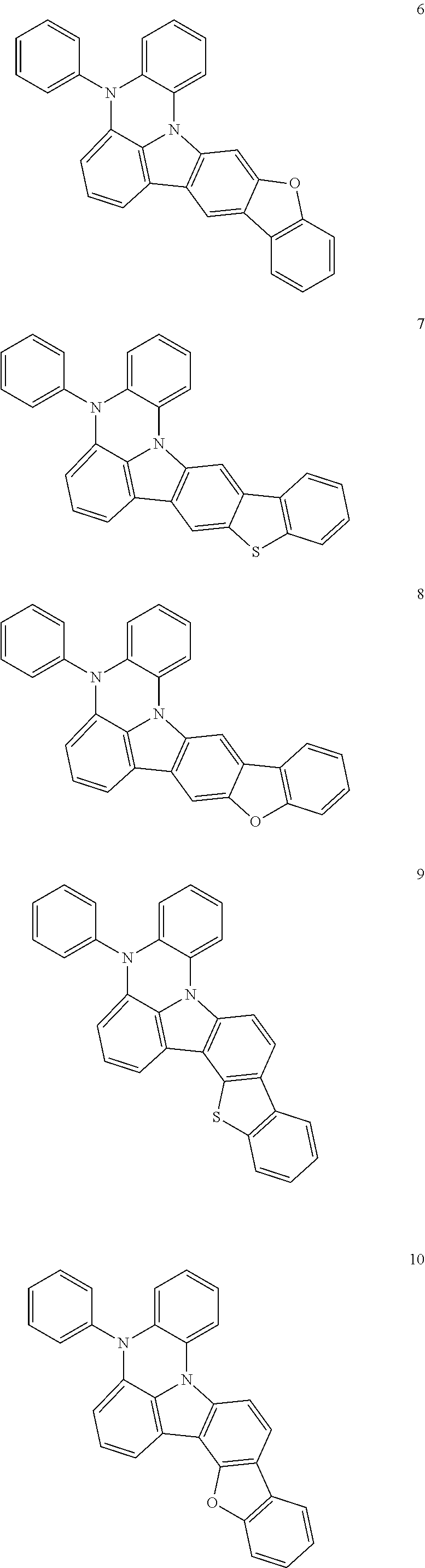


Hereinafter, an organic optoelectric device including the compound for an organic optoelectric device is described.
The organic optoelectric device may include a device to convert electrical energy into photoenergy or vice versa. For example, the device may include an organic photoelectric device, an organic light emitting diode, an organic solar cell, or an organic photo-conductor drum.
The embodiments may be realized by providing an organic optoelectric device including an anode and a cathode facing each other, and at least one organic layer between the anode and the cathode, wherein the organic layer includes the compound according to an embodiment.
The organic layer may include an emission layer, and the emission layer may include the compound.
The compound may be a host of the emission layer.
The organic layer may include at least one auxiliary layer selected from a hole injection layer, a hole transport layer, an electron blocking layer, an electron transport layer, an electron injection layer, or a hole blocking layer, and the at least one auxiliary layer may include the compound.
Herein, an organic light emitting diode as an example of an organic optoelectric device is described by referring to drawings.
Referring to FIGS. 1 and 2 , organic light emitting diodes 100 and 200 according to the embodiments may include an anode 120, a cathode 110, and at least one organic thin layer 105 between the anode and cathode.
The anode 120 may include an anode material having a large work function to facilitate hole injection into an organic thin layer. Examples of the anode material may include: a metal such as nickel, platinum, vanadium, chromium, copper, zinc, and gold, or alloys thereof; a metal oxide such as zinc oxide, indium oxide, indium tin oxide (ITO), and indium zinc oxide (IZO); a combined metal and oxide such as ZnO:Al or SnO2:Sb; or a conductive polymer such as poly(3-methylthiophene), poly[3,4-(ethylene-1,2-dioxy)thiophene] (PEDT), polypyrrole, and polyaniline. In an implementation, a transparent electrode including indium tin oxide (ITO) may be used as an anode.
The cathode 110 may include a cathode material having a small work function to facilitate electron injection into an organic thin layer. Examples of the cathode material may include a metal such as magnesium, calcium, sodium, potassium, titanium, indium, yttrium, lithium, gadolinium, aluminum, silver, tin, and lead, or alloys thereof; or a multi-layered material such as LiF/Al, Liq/Al, LiO2/Al, LiF/Ca, LiF/Al, and BaF2/Ca. In an implementation, a metal electrode including aluminum may be used as a cathode.
Referring to FIG. 1 , the organic light emitting diode 100 according to an embodiment may include an organic thin layer 105 including only an emission layer 130. For example, the organic thin layer 105 may include only a single layer.
Referring to FIG. 2 , an organic light emitting diode 200 according to another embodiment may further include a hole auxiliary layer 140 along with an emission layer 230. The hole auxiliary layer 140 may help increase hole injection and/or hole mobility between the anode 120 and the emission layer 230 and may help prevent or block electrons. The hole auxiliary layer 140 may be, e.g., a hole transport layer (HTL), a hole injection layer (HIL), and/or an electron blocking layer, and may include at least one layer. The compound according to an embodiment, described above, may be included in an emission layer 130, 230 and/or in a hole auxiliary layer 140. In an implementation, the organic thin layer 105 may further include, e.g., an electron injection layer (EIL), an electron transport layer (ETL), an auxiliary electron transport layer (ETL), an auxiliary hole transport layer (HTL), hole transport layer (HTL), a hole injection layer (HIL), and/or a combination thereof, even though they are not shown in FIG. 1 or 2 .
In FIGS. 1 and 2 , at least one organic thin layer 105 selected from the emission layer 130 and 230, the hole transport layer (HTL) 140, and the electron injection layer (EIL), the electron transport layer (ETL), the auxiliary electron transport layer (ETL), the auxiliary hole transport layer (HTL), the hole injection layer (HIL), or a combination thereof, may include the compound according to an embodiment.
For example, the compound may be used or included in the hole injection layer (HIL) or the hole transport layer (HTL).
The compound for an organic optoelectric device may be used or included in the emission layer, e.g., may be a host in the emission layer. For example, the compound may be a green phosphorescent host in the emission layer.
The organic light emitting diodes 100 and 200 may be manufactured by: forming an anode or a cathode on a substrate; forming an organic thin layer in accordance with a dry coating method such as evaporation, sputtering, plasma plating, and ion plating or a wet coating method such as spin coating, dipping, and flow coating; and providing a cathode or an anode thereon.
Another embodiment may provide a display device including the organic optoelectric device.
Preparation of Compounds for an Organic Optoelectric Device
Exemplary Synthesis of Compound for an Organic Optoelectric Device

Compounds according to an embodiment may generally be synthesized according to Reaction scheme 1, above. In Reaction Scheme 1, (A) represents a structure including a ring in which X is fused with neighboring X9 to X11 (fusion, indeno, and the like) as defined in the above Chemical Formulae I and II, and Y2 included in the (A) may be represented by C, N, O, S, S(═O), and S(═O)2, and R2 may be the same as defined in the above Chemical Formulas I and II.
Each step may be as follows.
Step 1: A compound (B) was prepared through Buchwald-Hartwig Cross Coupling Reaction by using commercially-available dibenzofuran, dibenzothiophene, carbazole, fluorene, and the like having the structure (A) and aniline having a halogen. This reaction may be performed without solvent or using a solvent such as toluene, xylene, 1,4-dioxane, or the like having no unfavorable influence thereon. The reaction may be performed at room or ambient temperature to an elevated temperature, e.g., at the elevated temperature. In the Buchwald-Hartwig Cross Coupling Reaction, various metal catalysts may be used, e.g., Pd(dba)2, Pd2(dba)3, and the like.
Step 2: An indeno compound (C) may be prepared by performing RCM (ring close metathesis) on the compound (B) obtained in the step 1 and then, a cyclization reaction under a metal-catalyst. The metal-catalyst in the reaction may include palladium (0), and tetrakis(triphenylphosphine) palladium (0) (PPh3)4Pd), palladium acetate (II) (Pd(OAc)2), tris(dibenzylideneacetone)dipalladium (0) (Pd2 dba3), bis(triphenylphosphine)palladium (II) chloride (PdCl2(PPh3)2), or the like may be used alone or as a composite with tributylphosphine (Bu3P). The reaction may be performed without using a ligand, or by using a ligand used for a cyclization reaction under a metal-catalyst, e.g., triphenylphosphine ((PPh3)4), 1,2-bis(diphenylphosphino)propane (DPPP), (R)-2,2′-bis(diphenylphosphino)-1,1′-binaphthyl (R)-BiNAP), or the like. Herein, a base such as potassium carbonate, sodium carbonate, silver carbonate, diethylisopropylamine, or the like may be used, and a solvent having no unfavorable influence on the reaction, e.g., N,N-dimethylformamide, benzene, xylene, acetonitrile, or the like may be used for the reaction. The reaction may be performed at ambient temperature to an elevated temperature, e.g., at an elevated temperature.
Step 3: An intermediate product (D) may be prepared by using the indeno intermediate product (C) cyclized in the step 2 and performing the same Buchwald-Hartwig Cross Coupling Reaction as the step 1.
Step 4: An intermediate product (E) was prepared by using the intermediate product (D) in the step 3 and performing the same RCM (ring close metathesis) as the step 2. The reaction may include various RCM reactions and may use various reagents, e.g., triphenylphosphine, triphenylphosphite, or the like, for cyclization. Herein, a solvent having no unfavorable influence on the reaction such as dimethylformamide or the like may be used, e.g., triphenylphosphite may be used alone, and the reaction may be performed at ambient temperature to an elevated temperature, e.g., at an elevated temperature.
Step 5: A final compound (F) in Reaction Scheme 1 may be synthesized by using the indeno compound (E) prepared in the step 4 with R2 having halogen especially when Y1 was nitrogen and performing the same Buchwald-Hartwig Cross Coupling Reaction as the step 1.
The following Examples and Comparative Examples are provided in order to highlight characteristics of one or more embodiments, but it will be understood that the Examples and Comparative Examples are not to be construed as limiting the scope of the embodiments, nor are the Comparative Examples to be construed as being outside the scope of the embodiments. Further, it will be understood that the embodiments are not limited to the particular details described in the Examples and Comparative Examples.
Compound 75 ((4,6-diphenyl-1,3,5-triazin-2-yl)-16H-benzofuro[3′,2′:6,7]indolo[3,2,1-de]phenazine) as an example of a compound for an organic optoelectric device according to an embodiment was synthesized through 5 steps shown in the following Reaction Scheme.

4-bromodibenzofuran (A) (30 g, 121.41 mmol) was put in xylene (500 ml), and 2-chloroaniline (16.23 g, 127.48 mmol), Pd2(dba)3 (3.34 g, 3.64 mmol), P(t-Bu)3 (1.74 ml, 7.28 mmol), and NaO(t-bu) (23.34 g, 242.83 mmol) were added thereto at ambient temperature, and the mixture was then refluxed and agitated for 14 hours. When the reaction was complete, the subject compound (B) (31.4 g, 88%) was obtained by adding water and ethyl acetate to the resultant, drying a separated organic layer with a silica gel filter and anhydrous magnesium sulfate and then, concentrating a solvent under a reduced pressure to obtain a mixture, and recrystallizing the mixture with dichloromethane and hexane.
The compound (B) (31 g, 105.53 mmol) prepared in the step 1 was dissolved in N,N-dimethylformamide (280 ml), and 10% Pd—C (7.11 g, 31.66 mmol), 1,3-bis(diphenylphosphino)propane (13.058 g, 31.66 mmol), t-tributylphosphine (52.07 ml, 105.53 mmol), and K2CO3 (29.17 g, 211.06 mmol) were added thereto. The mixture was then refluxed and agitated for 24 hours. When the reaction was complete, the subject compound (C) (20.64 g, 76%) was obtained by adding water and ethyl acetate to the resultant, drying a separated organic layer with a silica gel filter and anhydrous magnesium sulfate and then, concentrating a solvent therein under a reduced pressure to obtain a mixture, and recrystallizing the mixture with dichloromethane and hexane.
The compound (C) (20 g, 77.73 mmol) prepared in the step 2 was dissolved in toluene, and 1-bromo-2-nitrobenzene (16.49 g, 81.62 mmol), Pd2(dba)3 (2.14 g, 2.33 mmol), P(t-Bu)3 (1.11 ml, 4.66 mmol), and NaO(t-bu) (14.94 g, 155.47 mmol) were added thereto at ambient temperature. The mixture was then refluxed and agitated for 18 hours. When the reaction was complete, the subject compound (D) (24.12 g, 82%) was obtained by adding water and ethyl acetate to the resultant, drying a separated organic layer with a silica gel filter and anhydrous magnesium sulfate and then, concentrating a solvent under a reduced pressure to obtain a mixture, and recrystallizing the mixture with dichloromethane and acetone.
The compound (D) (24 g, 91.56 mmol) prepared in the step 3 was dissolved in triethylphosphite (55 ml), and the mixture was refluxed and agitated for 4 hours. When the reaction was complete, the subject compound (E) (15.82 g, 72%) was obtained by recrystallizing the mixture with dichloromethane and ethyl acetate after removing triethylphosphite therefrom.
The compound (E) (15 g, 43.31 mmol) obtained in the step 4 was dissolved in xylene (180 ml), and 2-bromo-4,6-diphenyl-[1,3,5]triazine (14.20 g, 45.47 mmol), Pd2(dba)3 (1.19 g, 1.30 mmol), P(t-Bu)3 (0.68 ml, 2.60 mmol), and NaO(t-bu) (8.23 g, 86.61 mmol) were added thereto at ambient temperature. The mixture was then refluxed and agitated for 13 hours. When the reaction was complete, Compound 75, i.e., (4,6-diphenyl-1,3,5-triazin-2-yl)-16H-benzofuro[3′,2′:6,7]indolo[3,2,1-de]phenazine, (18.26 g, 73%) was obtained by adding water and ethyl acetate thereto, drying a separated organic layer with a silica gel filter and anhydrous magnesium sulfate and then, concentrating a solvent under a reduced pressure to obtain a mixture, and recrystallizing the mixture with toluene.
Molecular formula: C39H23N5O
Molecular formula: C39H23N5O
HRMS (70 eV, EI+): m/z calculation value (577.19), measurement value (577)

1-bromo-9H-carbazole (30 g, 121.90 mmol, CAS no. 16807-11-7) was dissolved in xylene (900 ml), and iodobenzene (29.84 g, 146.28 mmol), Pd2(dba)3 (3.35 g, 3.66 mmol), P(t-Bu)3 (5.22 ml, 10.97 mmol), and NaO(t-bu) (17.57 g, 182.85 mmol) were added thereto at ambient temperature. The mixture was then refluxed and agitated for 13 hours. When the reaction was complete, the subject compound (B) (32.21 g, 82%) was obtained by adding water and ethyl acetate to the resultant, drying a separated organic layer with a silica gel filter and anhydrous magnesium sulfate and concentrating a solvent under a reduced pressure to obtain a mixture, and recrystallizing the mixture with ethyl acetate and hexane.
Compound 248, i.e., (4,6-diphenyl-1,3,5-triazin-2-yl)-10-phenyl-10,16-dihydroindolo[3′,2′:6,7] indolo[3,2,1-de]phenazine, (16.6 g) was obtained by using the compound (B) (32.21 g, 99.32 mmol) prepared in the step 1 of Synthesis Example 2 through the same steps 2, 3, 4, and 5 as described above in Synthesis Example 1.
Molecular formula: C45H28N6
Molecular formula: C45H28N6
HRMS (70 eV, EI+): m/z calculation value (652.24), measurement value 652

Compound 249, i.e., (4,6-diphenyl-1,3,5-triazin-2-yl)-6-phenyl-6,16-dihydroindolo[2′,3′:6,7]indolo[3,2,1-de]phenazine, (14.2 g) was obtained by using 4-bromo-9H-carbazole (30 g, 121.90 mmol, CAS no. 3652-89-9) through the same step 1 of Synthesis Example 2 and the same steps 2, 3, 4, and 5 as Synthesis Example 1.
Molecular formula: C45H28N6
Molecular formula: C45H28N6
HRMS (70 eV, EI+): m/z calculation value (652.24), measurement value 652


3-bromo-9H-carbazole (28.4 g, 116 mmol, CAS no. 1592-95-6) was dissolved in dimethylformamide (300 ml), and 2-chloro-4,6-diphenyl-1,3,5-triazine (31.0 g, 116 mmol) and K2CO3 (32 g, 116 mmol) were added thereto at ambient temperature. Then, the mixture was refluxed and agitated for 13 hours. When the reaction was complete, the subject compound (B) (25.0 g, 90%) was obtained by adding water and ethyl acetate to the resultant, drying a separated organic layer with a silica gel filter and anhydrous magnesium sulfate and concentrating a solvent under a reduced pressure to obtain a mixture, and recrystallizing the mixture with toluene.
The subject compound (C) (17.5 g) was obtained by using the compound (B) (25 g, 52.37 mmol) obtained in the step 1 of Synthesis Example 4 through the steps 2, 3, and 4 of Synthesis Example 1.
The compound (C) (17 g, 29.48 mmol) obtained in the step 2 of Synthesis Example 4 was dissolved in xylene (216 ml), and iodobenzene (7.22 g, 35.38 mmol), Pd2(dba)3 (0.81 g, 0.88 mmol), P(t-Bu)3 (1.26 ml, 2.65 mmol), and NaO(t-bu) (4.25 g, 44.22 mmol) were added thereto at ambient temperature. The mixture was refluxed and agitated for 13 hours. When the reaction was complete, Compound 257, i.e., (4,6-diphenyl-1,3,5-triazin-2-yl)-5-phenyl-5,10-dihydroindolo[2′,3′:5,6]indolo[3,2,1-de]phenazine, (14.82 g, 77%) was obtained by adding water and ethyl acetate to the resultant, drying a separated organic layer with a silica gel filter and anhydrous magnesium sulfate and concentrating a solvent under a reduced pressure to obtain a mixture, and recrystallizing the mixture with toluene.
Molecular formula: C45H28N6
Molecular formula: C45H28N6
HRMS (70 eV, EI+): m/z calculation value (652.24), measurement value 652
(Comparison of Simulation Characteristics of Compounds)
Energy level of each compound was measured by using a super computer GAIA (IBM power 6) in a Gaussian 09 method, and the results are provided in the following Table 1.
| TABLE 1 | ||||
| Compound | T1 (eV) | S1 (eV) | HOMO (eV) | LUMO (eV) |
| Synthesis Example 1 | 2.805 | 2.952 | −5.201 | −1.715 |
| (Compound 75) | ||||
| Synthesis Example 2 | 2.804 | 2.916 | −5.121 | −1.720 |
| (Compound 248) | ||||
| Synthesis Example 3 | 2.825 | 2.940 | −5.094 | −1.658 |
| (Compound 249) | ||||
| Synthesis Example 4 | 2.219 | 2.240 | −4.426 | −1.834 |
| (Compound 257) | ||||
| CBP | 2.971 | 3.457 | −5.319 | −1.231 |
(Manufacture of Organic Light Emitting Diode)
An organic light emitting diode was manufactured by using Compound 75 obtained in Synthesis Example 1 as a host and Ir(PPy)3 as a dopant.
A 1,000 Å-thick ITO layer was used as an anode, and a 1,000 Å-thick aluminum (Al) layer was used as a cathode. Specifically, the anode was manufactured by cutting an ITO glass substrate having sheet resistance of 15 Ω/cm2 into a size of 50 mm×50 mm×0.7 mm and washing it with a ultrasonic wave in acetone, isopropyl alcohol, and pure water respectively for 15 minutes and then, with UV ozone for 30 minutes.
On the anode, an 800 Å-thick hole transport layer (HTL) was formed by depositing N4,N4′-di(naphthalen-1-yl)-N4,N4′-diphenylbiphenyl-4,4′-diamine (NPB) (80 nm) under a vacuum degree of 650×10−7 Pa at a deposition rate of 0.1 to 0.3 nm/s. Subsequently, a 300 Å-thick emission layer was formed by using Compound 75 obtained in Synthesis Example 1 as a host and Ir(PPy)3 as a phosphorescent dopant, by simultaneously depositing the host and dopant. The phosphorescent dopant was deposited in an amount of 7 wt %, based on 100 wt % of the emission layer by adjusting its deposition rate.
On the emission layer, a 50 Å-thick hole-blocking layer was formed by depositing bis(2-methyl-8-quinolinolate)-4-(phenylphenolato)aluminium (BAlq) under the same deposition condition. Subsequently, a 200 Å-thick electron transport layer (ETL) was formed by depositing Alq3 under the same deposition condition. On the electron transport layer (ETL), the cathode was formed by sequentially depositing LiF and Al, manufacturing an organic light emitting diode.
The organic light emitting diode had a structure of ITO/NPB (80 nm)/EML (compound 75 (93 wt %)+Ir(PPy)3 (7 wt %), 30 nm)/Balq (5 nm)/Alq3 (20 nm)/LiF (1 nm)/Al (100 nm).
An organic light emitting diode was manufactured according to the same method as Example 1, except for using Compound 248 of Synthesis Example 2 instead of Compound 75 of Synthesis Example 1.
An organic light emitting diode was manufactured according to the same method as Example 1, except for using Compound 249 of Synthesis Example 3 instead of Compound 75 of Synthesis Example 1.
An organic light emitting diode was manufactured according to the same method as Example 1, except for using Compound 257 of Synthesis Example 4 instead of Compound 75 of Synthesis Example 1.
An organic light emitting diode was manufactured according to the same method as Example 1, except for using CBP having the following structure, instead of Compound 75 of Synthesis Example 1.
NPB, BAlq, CBP, and Ir(PPy)3 used to manufacture the organic light emitting diode have the following structure.

(Performance Measurement of Organic Light Emitting Diode)
Current density and luminance changes depending on a voltage and luminous efficiency of each organic light emitting diode according to Examples 1 to 4 and Comparative Example 1 were measured.
The measurements were specifically performed in the following method, and the results were provided in the following Table 2.
(1) Measurement of Current Density Change Depending on Voltage Change
The manufactured organic light emitting diodes were measured for current value flowing in the unit device, while increasing the voltage from 0 V to 10 V using a current-voltage meter (Keithley 2400), and the measured current value was divided by an area to provide the results.
(2) Measurement of Luminance Change Depending on Voltage Change
The manufactured organic light emitting diodes were measured for luminance, while increasing the voltage from 0 V to 10 V using a luminance meter (Minolta Cs-1000A).
(3) Measurement of Luminous Efficiency
Current efficiency (cd/A) at the same current density (10 mA/cm2) were calculated by using the luminance, current density, and voltages (V) from the items (1) and (2).
(4) Measurement of Life-Span
Life-span of the organic light emitting diode was evaluated by maintaining luminance (cd/m2) at 5,000 cd/m2 and measuring time taken until current efficiency (cd/A) decreased down to 90%.
| TABLE 2 | |||||
| 90% life- | |||||
| Driving | Effi- | span (h) | |||
| volt- | Color | ciency | at 5,000 | ||
| No. | Emission layer | age (V) | (EL color) | (cd/A) | cd/m2 |
| Example 1 | Compound 75 | 3.7 | Green | 66.4 | 180 |
| Example 2 | Compound 248 | 3.5 | Green | 69.5 | 165 |
| Example 3 | Compound 249 | 3.5 | Green | 77.8 | 160 |
| Example 4 | Compound 257 | 4.7 | Green | 48.2 | 76 |
| Comparative | CBP | 4.8 | Green | 31.4 | 40 |
| Example 1 | |||||
As shown in Table 2, the organic light emitting diodes according to Examples 1 to 4 showed improved characteristics in terms of a driving voltage, luminous efficiency, and/or power efficiency, compared with the organic light emitting diode according to Comparative Example 1.
- 100: organic light emitting diode
- 200: organic light emitting diode
- 110: cathode
- 120: anode
- 105: organic thin layer
- 130: emission layer
- 230: emission layer
- 140: hole transport layer (HTL)
By way of summation and review, performance of an organic light emitting diode may be affected by characteristics of the organic layer, e.g., may be mainly affected by characteristics of an organic material of the organic layer.
For example, an organic material that is capable of increasing hole and electron mobility and simultaneously increasing electrochemical stability may be used so that an organic light emitting diode may be applied to a large-size flat panel display.
The embodiments may provide a compound for an organic optoelectric device that realizes an organic optoelectric device having characteristics such as high efficiency, long life-span, and the like.
An organic optoelectric device including the compound for an organic optoelectric device according to one embodiment may have excellent electrochemical and thermal stability, excellent life-span characteristics, and high luminous efficiency at a low driving voltage. In addition, the compound for an organic optoelectric device may be appropriate for a solution process.
Example embodiments have been disclosed herein, and although specific terms are employed, they are used and are to be interpreted in a generic and descriptive sense only and not for purpose of limitation. In some instances, as would be apparent to one of ordinary skill in the art as of the filing of the present application, features, characteristics, and/or elements described in connection with a particular embodiment may be used singly or in combination with features, characteristics, and/or elements described in connection with other embodiments unless otherwise specifically indicated. Accordingly, it will be understood by those of skill in the art that various changes in form and details may be made without departing from the spirit and scope of the present invention as set forth in the following claims.
Claims (16)
1. A compound for an organic optoelectric device, the compound including a combination of a moiety represented by the following Chemical Formula I and a moiety represented by the following Chemical Formula II:

wherein, in the above Chemical Formula I and Chemical Formula II,
X1 to X7 are each independently CRa or N, provided that all X1 to X7 are CRa or one of X1 to X7 is N,
Y is O, S, SO2, PO, or N-L2-R4,
two *s of the above Chemical Formula II are bonded with two adjacent *s of the above Chemical Formula I,
*s in the above Chemical Formula I that are not bonded with the two *s of the above Chemical Formula II are each independently CRb or N,
L1 and L2 are each independently a single bond, a substituted or unsubstituted C1 to C30 alkylene group, a substituted or unsubstituted C3 to C30 cycloalkylene group, a substituted or unsubstituted C3 to C30 heterocycloalkylene group, a substituted or unsubstituted C6 to C30 arylene group, a substituted or unsubstituted C3 to C30 heteroarylene group, a substituted or unsubstituted C6 to C30 aryleneamine group, a substituted or unsubstituted C6 to C30 heteroaryleneamine group, a substituted or unsubstituted C1 to C30 alkoxylene group, a substituted or unsubstituted C6 to C30 aryloxylene group, a substituted or unsubstituted C2 to C30 alkenylene group, a substituted or unsubstituted C2 to C30 alkynylene group, or a combination thereof, and
R1 to R6, Ra, and Rb are each independently hydrogen, deuterium, a halogen, a cyano group, a hydroxyl group, an amino group, a substituted or unsubstituted C1 to C20 amine group, a nitro group, a carboxyl group, a ferrocenyl group, a substituted or unsubstituted C1 to C20 alkyl group, a substituted or unsubstituted C6 to C30 aryl group, a substituted or unsubstituted C2 to C30 heteroaryl group, a substituted or unsubstituted C1 to C20 alkoxy group, a substituted or unsubstituted C6 to C20 aryloxy group, a substituted or unsubstituted C3 to C40 silyloxy group, a substituted or unsubstituted C1 to C20 acyl group, a substituted or unsubstituted C2 to C20 alkoxycarbonyl group, a substituted or unsubstituted C2 to C20 acyloxy group, a substituted or unsubstituted C2 to C20 acylamino group, a substituted or unsubstituted C2 to C20 alkoxycarbonylamino group, a substituted or unsubstituted C7 to C20 aryloxycarbonylamino group, a substituted or unsubstituted C1 to C20 sulfamoylamino group, a substituted or unsubstituted C1 to C20 sulfonyl group, a substituted or unsubstituted C1 to C20 alkylthiol group, a substituted or unsubstituted C6 to C20 arylthiol group, a substituted or unsubstituted C1 to C20 heterocyclothiol group, a substituted or unsubstituted C1 to C20 ureide group, a substituted or unsubstituted C3 to C40 silyl group, a substituted or unsubstituted C3 to C40 fused ring-containing group, or a combination thereof.
2. The compound for an organic optoelectric device as claimed in claim 1 , wherein the compound is represented by one of the following Chemical Formula 1 to Chemical Formula 6:


wherein, in the above Chemical Formula 1 to Chemical Formula 6,
X1 to X9 are each independently CRa or N, provided that all X1 to X9 are CRa or one of X1 to X9 is N,
Y is O, S, SO2, PO, or N-L2-R4,
L1 and L2 are each independently a single bond, a substituted or unsubstituted C1 to C30 alkylene group, a substituted or unsubstituted C3 to C30 cycloalkylene group, a substituted or unsubstituted C3 to C30 heterocycloalkylene group, a substituted or unsubstituted C6 to C30 arylene group, or a substituted or unsubstituted C3 to C30 heteroarylene group, a substituted or unsubstituted C6 to C30 aryleneamine group, a substituted or unsubstituted C6 to C30 heteroaryleneamine group, a substituted or unsubstituted C1 to C30 alkoxylene group, a substituted or unsubstituted C6 to C30 aryloxylene group, a substituted or unsubstituted C2 to C30 alkenylene group, a substituted or unsubstituted C2 to C30 alkynylene group, or a combination thereof, and
R1 to R6 and Ra are each independently hydrogen, deuterium, a halogen, a cyano group, a hydroxyl group, an amino group, a substituted or unsubstituted C1 to C20 amine group, a nitro group, a carboxyl group, a ferrocenyl group, a substituted or unsubstituted C1 to C20 alkyl group, a substituted or unsubstituted C6 to C30 aryl group, a substituted or unsubstituted C2 to C30 heteroaryl group, a substituted or unsubstituted C1 to C20 alkoxy group, a substituted or unsubstituted C6 to C20 aryloxy group, a substituted or unsubstituted C3 to C40 silyloxy group, a substituted or unsubstituted C1 to C20 acyl group, a substituted or unsubstituted C2 to C20 alkoxycarbonyl group, a substituted or unsubstituted C2 to C20 acyloxy group, a substituted or unsubstituted C2 to C20 acylamino group, a substituted or unsubstituted C2 to C20 alkoxycarbonylamino group, a substituted or unsubstituted C7 to C20 aryloxycarbonylamino group, a substituted or unsubstituted C1 to C20 sulfamoylamino group, a substituted or unsubstituted C1 to C20 sulfonyl group, a substituted or unsubstituted C1 to C20 alkylthiol group, a substituted or unsubstituted C6 to C20 arylthiol group, a substituted or unsubstituted C1 to C20 heterocyclothiol group, a substituted or unsubstituted C1 to C20 ureide group, a substituted or unsubstituted C3 to C40 silyl group, a substituted or unsubstituted C3 to C40 fused ring-containing group, or a combination thereof.
3. The compound for an organic optoelectric device as claimed in claim 1 , wherein:
Y is O, S, or N-L2-R4, and
R1 and R4 are each independently a functional group of the following Group I:

wherein, in Group I,
each Z is independently N or CRc,
W is O, S, SO, SO2, NR′, CR′R″, or SiR′R″,
Rc, R′, and R″ are each independently hydrogen, deuterium, a substituted or unsubstituted C1 to C30 alkyl group, a substituted or unsubstituted C3 to C30 cycloalkyl group, a substituted or unsubstituted C3 to C30 heterocycloalkyl group, a substituted or unsubstituted C6 to C30 aryl group, a substituted or unsubstituted C3 to C30 heteroaryl group, a substituted or unsubstituted amine group, a substituted or unsubstituted C6 to C30 arylamine group, a substituted or unsubstituted C6 to C30 heteroarylamine group, a substituted or unsubstituted C1 to C30 alkoxy group, a substituted or unsubstituted C2 to C30 alkoxycarbonyl group, a substituted or unsubstituted C2 to C30 alkoxycarbonylamino group, a substituted or unsubstituted C7 to C30 aryloxycarbonylamino group, a substituted or unsubstituted C1 to C30 sulfamoylamino group, a substituted or unsubstituted C2 to C30 alkenyl group, a substituted or unsubstituted C2 to C30 alkynyl group, a substituted or unsubstituted silyl group, a substituted or unsubstituted silyloxy group, a substituted or unsubstituted C1 to C30 acyl group, a substituted or unsubstituted C1 to C20 acyloxy group, a substituted or unsubstituted C1 to C20 acylamino group, a substituted or unsubstituted C1 to C30 sulfonyl group, a substituted or unsubstituted C1 to C30 alkylthiol group, a substituted or unsubstituted C1 to C30 heterocyclothiol group, a substituted or unsubstituted C6 to C30 arylthiol group, a substituted or unsubstituted C1 to C30 heteroarylthiol group, a substituted or unsubstituted C1 to C30 ureide group, a halogen, a halogen-containing group, a cyano group, a hydroxyl group, an amino group, a nitro group, a carboxyl group, a ferrocenyl group, or a combination thereof, and
* is a binding site.
4. The compound for an organic optoelectric device as claimed in claim 1 , wherein R1 and R4 are each independently a substituted or unsubstituted functional group of the following Group II:


wherein, in Group II,
RC, R′ and R″ are each independently hydrogen, deuterium, a substituted or unsubstituted C1 to C30 alkyl group, a substituted or unsubstituted C3 to C30 cycloalkyl group, a substituted or unsubstituted C3 to C30 heterocycloalkyl group, a substituted or unsubstituted C6 to C30 aryl group, a substituted or unsubstituted C3 to C30 heteroaryl group, a substituted or unsubstituted C2 to C30 alkenyl group, a substituted or unsubstituted C2 to C30 alkynyl group, a substituted or unsubstituted silyl group, a substituted or unsubstituted silyloxy group, a halogen, a halogen-containing group, a cyano group, a hydroxyl group, an amino group, a nitro group, a carboxyl group, a ferrocenyl group, or a combination thereof, and
* is a binding site.
5. The compound for an organic optoelectric device as claimed in claim 1 , wherein L1 and L2 are each independently a single bond, a substituted or unsubstituted phenylene group, a substituted or unsubstituted naphthylene group, a substituted or unsubstituted anthracenylene group, or a substituted or unsubstituted biphenylene group.
6. The compound for an organic optoelectric device as claimed in claim 1 , wherein the compound is represented by one of the following Chemical Formula 7 to Chemical Formula 24:


wherein, in the above Chemical Formula 7 to Chemical Formula 24,
Y is O, S, or N-L2-R4,
L2 is a single bond, a substituted or unsubstituted C1 to C30 alkylene group, a substituted or unsubstituted C3 to C30 cycloalkylene group, a substituted or unsubstituted C3 to C30 heterocycloalkylene group, a substituted or unsubstituted C6 to C30 arylene group, or a substituted or unsubstituted C3 to C30 heteroarylene group, a substituted or unsubstituted C6 to C30 aryleneamine group, a substituted or unsubstituted C6 to C30 heteroaryleneamine group, a substituted or unsubstituted C1 to C30 alkoxylene group, a substituted or unsubstituted C6 to C30 aryloxylene group, a substituted or unsubstituted C2 to C30 alkenylene group, a substituted or unsubstituted C2 to C30 alkynylene group, or a combination thereof, and
R1 and R4 are each independently hydrogen, deuterium, a halogen, a cyano group, a hydroxyl group, an amino group, a substituted or unsubstituted C1 to C20 amine group, a nitro group, a carboxyl group, a ferrocenyl group, a substituted or unsubstituted C1 to C20 alkyl group, a substituted or unsubstituted C6 to C30 aryl group, a substituted or unsubstituted C2 to C30 heteroaryl group, a substituted or unsubstituted C1 to C20 alkoxy group, a substituted or unsubstituted C6 to C20 aryloxy group, a substituted or unsubstituted C3 to C40 silyloxy group, a substituted or unsubstituted C1 to C20 acyl group, a substituted or unsubstituted C2 to C20 alkoxycarbonyl group, a substituted or unsubstituted C2 to C20 acyloxy group, a substituted or unsubstituted C2 to C20 acylamino group, a substituted or unsubstituted C2 to C20 alkoxycarbonylamino group, a substituted or unsubstituted C7 to C20 aryloxycarbonylamino group, a substituted or unsubstituted C1 to C20 sulfamoylamino group, a substituted or unsubstituted C1 to C20 sulfonyl group, a substituted or unsubstituted C1 to C20 alkylthiol group, a substituted or unsubstituted C6 to C20 arylthiol group, a substituted or unsubstituted C1 to C20 heterocyclothiol group, a substituted or unsubstituted C1 to C20 ureide group, a substituted or unsubstituted C3 to C40 silyl group, a substituted or unsubstituted C3 to C40 fused ring-containing group, or a combination thereof.
7. The compound for an organic optoelectric device as claimed in claim 1 , wherein the compound is represented by one of the following Chemical Formula 25 to Chemical Formula 54:


wherein, in the above Chemical Formula 25 to Chemical Formula 54,
L1 is a single bond, a substituted or unsubstituted C6 to C30 arylene group, or a substituted or unsubstituted C3 to C30 heteroarylene group, and
R1 and R4 are each independently hydrogen, deuterium, a substituted or unsubstituted C1 to C20 alkyl group, a substituted or unsubstituted C6 to C30 aryl group, or a substituted or unsubstituted C2 to C30 heteroaryl group.
8. The compound for an organic optoelectric device as claimed in claim 1 , wherein:
Y is O, S or N-L2-R4,
L1 and L2 are each independently a single bond, a substituted or unsubstituted C6 to C30 arylene group, or a substituted or unsubstituted C3 to C30 heteroarylene group, and
R1 to R6, Ra, and Rb are each independently hydrogen, deuterium, a substituted or unsubstituted C1 to C20 alkyl group, a substituted or unsubstituted C6 to C30 aryl group, or a substituted or unsubstituted C2 to C30 heteroaryl group.
9. The compound for an organic optoelectric device as claimed in claim 1 , wherein R1 and R4 is a substituted or unsubstituted phenyl group, a substituted or unsubstituted biphenyl group, a substituted or unsubstituted fluorenyl group, a substituted or unsubstituted pyridyl group, a substituted or unsubstituted pyrimidinyl group, a substituted or unsubstituted triazinyl group, a substituted or unsubstituted dibenzofuranyl group, a substituted or unsubstituted dibenzothiophenyl group, or a substituted or unsubstituted carbazolyl group.
10. The compound for an organic optoelectric device as claimed in claim 1 , wherein:
L1 and L2 are each independently a single bond, a substituted or unsubstituted phenylene group, a substituted or unsubstituted biphenylene group, a substituted or unsubstituted fluorenylene group, a substituted or unsubstituted pyridylene group, a substituted or unsubstituted pyrimidinylene group, a substituted or unsubstituted triazinylene group, a substituted or unsubstituted dibenzofuranylene group, a substituted or unsubstituted dibenzothiophenylene group, or a substituted or unsubstituted carbazolylene group, and
R1 to R6, Ra, and Rb are each independently hydrogen, deuterium, a substituted or unsubstituted phenyl group, a substituted or unsubstituted biphenyl group, a substituted or unsubstituted fluorenyl group, a substituted or unsubstituted pyridyl group, a substituted or unsubstituted pyrimidinyl group, a substituted or unsubstituted triazinyl group, a substituted or unsubstituted dibenzofuranyl group, a substituted or unsubstituted dibenzothiophenyl group, or a substituted or unsubstituted carbazolyl group.
11. The compound for an organic optoelectric device as claimed in claim 1 , wherein the compound is one of the following Compounds 75, 248, 249, and 257:

12. An organic optoelectric device, comprising:
an anode and a cathode facing each other, and
at least one organic layer between the anode and the cathode,
wherein the organic layer includes the compound as claimed in claim 1 .
13. The organic optoelectric device as claimed in claim 12 , wherein:
the organic layer includes an emission layer, and
the emission layer includes the compound.
14. The organic optoelectric device as claimed in claim 13 , wherein the compound is a host of the emission layer.
15. The organic optoelectric device as claimed in claim 12 , wherein:
the organic layer includes at least one auxiliary layer selected from a hole injection layer, a hole transport layer, an electron blocking layer, an electron transport layer, an electron injection layer, or a hole blocking layer, and
the at least one auxiliary layer includes the compound.
16. A display device comprising the organic optoelectric device as claimed in claim 12 .
Applications Claiming Priority (2)
| Application Number | Priority Date | Filing Date | Title |
|---|---|---|---|
| KR1020130106803A KR101759238B1 (en) | 2013-09-05 | 2013-09-05 | Compound for optoelectric device, organic optoelectric device including the same, and display device |
| KR10-2013-0106803 | 2013-09-05 |
Publications (2)
| Publication Number | Publication Date |
|---|---|
| US20150060788A1 US20150060788A1 (en) | 2015-03-05 |
| US9543528B2 true US9543528B2 (en) | 2017-01-10 |
Family
ID=52581865
Family Applications (1)
| Application Number | Title | Priority Date | Filing Date |
|---|---|---|---|
| US14/283,935 Active 2035-06-23 US9543528B2 (en) | 2013-09-05 | 2014-05-21 | Compound for an organic optoelectric device, organic optoelectric device including the same, and display device including the optoelectric device |
Country Status (2)
| Country | Link |
|---|---|
| US (1) | US9543528B2 (en) |
| KR (1) | KR101759238B1 (en) |
Families Citing this family (2)
| Publication number | Priority date | Publication date | Assignee | Title |
|---|---|---|---|---|
| KR102032267B1 (en) * | 2016-03-30 | 2019-11-08 | 덕산네오룩스 주식회사 | Compound for organic electronic element, organic electronic element using the same, and an electronic device thereof |
| KR102469683B1 (en) * | 2017-12-21 | 2022-11-23 | 덕산네오룩스 주식회사 | Compound for organic electronic element, organic electronic element comprising the same, and electronic device thereof |
Citations (12)
| Publication number | Priority date | Publication date | Assignee | Title |
|---|---|---|---|---|
| WO2008006454A1 (en) | 2006-07-11 | 2008-01-17 | Merck Patent Gmbh | Electroluminescent polymers and use thereof |
| WO2009148015A1 (en) | 2008-06-05 | 2009-12-10 | 出光興産株式会社 | Halogen compound, polycyclic compound, and organic electroluminescence element comprising the polycyclic compound |
| JP2010126535A (en) | 2008-11-28 | 2010-06-10 | Samsung Electronics Co Ltd | Compound comprising phosphorescence unit, light emitting polymer and organic light emitting device comprising light emitting polymer |
| WO2010113761A1 (en) | 2009-03-31 | 2010-10-07 | 新日鐵化学株式会社 | Organic electroluminescent device |
| WO2011088877A1 (en) | 2010-01-25 | 2011-07-28 | Merck Patent Gmbh | Compounds for electronic devices |
| WO2011107186A2 (en) | 2010-03-02 | 2011-09-09 | Merck Patent Gmbh | Compounds for electronic devices |
| WO2011125020A1 (en) | 2010-04-06 | 2011-10-13 | Basf Se | Substituted carbazole derivatives and use thereof in organic electronics |
| WO2011128017A1 (en) | 2010-04-14 | 2011-10-20 | Merck Patent Gmbh | Bridged triarylamines and -phosphines as materials for electronic devices |
| WO2012067415A2 (en) * | 2010-11-19 | 2012-05-24 | 덕산하이메탈(주) | Compound and organic electronic device using same, and terminal comprising the organic electronic device |
| KR20120079411A (en) | 2011-01-04 | 2012-07-12 | 주식회사 두산 | Phenazine-based compound and organic electroluminescent device comprising the same |
| JP2012234873A (en) | 2011-04-28 | 2012-11-29 | Konica Minolta Holdings Inc | Organic electroluminescent element material, organic electroluminescent element, display device, and lighting device |
| JP2012248663A (en) | 2011-05-27 | 2012-12-13 | Konica Minolta Holdings Inc | Organic electroluminescent element material, organic electroluminescent element, display device, lighting device, and compound |
-
2013
- 2013-09-05 KR KR1020130106803A patent/KR101759238B1/en active Active
-
2014
- 2014-05-21 US US14/283,935 patent/US9543528B2/en active Active
Patent Citations (14)
| Publication number | Priority date | Publication date | Assignee | Title |
|---|---|---|---|---|
| WO2008006454A1 (en) | 2006-07-11 | 2008-01-17 | Merck Patent Gmbh | Electroluminescent polymers and use thereof |
| JP2009542868A (en) | 2006-07-11 | 2009-12-03 | メルク パテント ゲーエムベーハー | Electroluminescent polymer and use thereof |
| WO2009148015A1 (en) | 2008-06-05 | 2009-12-10 | 出光興産株式会社 | Halogen compound, polycyclic compound, and organic electroluminescence element comprising the polycyclic compound |
| JP2010126535A (en) | 2008-11-28 | 2010-06-10 | Samsung Electronics Co Ltd | Compound comprising phosphorescence unit, light emitting polymer and organic light emitting device comprising light emitting polymer |
| WO2010113761A1 (en) | 2009-03-31 | 2010-10-07 | 新日鐵化学株式会社 | Organic electroluminescent device |
| WO2011088877A1 (en) | 2010-01-25 | 2011-07-28 | Merck Patent Gmbh | Compounds for electronic devices |
| WO2011107186A2 (en) | 2010-03-02 | 2011-09-09 | Merck Patent Gmbh | Compounds for electronic devices |
| WO2011125020A1 (en) | 2010-04-06 | 2011-10-13 | Basf Se | Substituted carbazole derivatives and use thereof in organic electronics |
| WO2011128017A1 (en) | 2010-04-14 | 2011-10-20 | Merck Patent Gmbh | Bridged triarylamines and -phosphines as materials for electronic devices |
| WO2012067415A2 (en) * | 2010-11-19 | 2012-05-24 | 덕산하이메탈(주) | Compound and organic electronic device using same, and terminal comprising the organic electronic device |
| KR20120054154A (en) | 2010-11-19 | 2012-05-30 | 덕산하이메탈(주) | Chemical and organic electronic element using the same, terminal thereof |
| KR20120079411A (en) | 2011-01-04 | 2012-07-12 | 주식회사 두산 | Phenazine-based compound and organic electroluminescent device comprising the same |
| JP2012234873A (en) | 2011-04-28 | 2012-11-29 | Konica Minolta Holdings Inc | Organic electroluminescent element material, organic electroluminescent element, display device, and lighting device |
| JP2012248663A (en) | 2011-05-27 | 2012-12-13 | Konica Minolta Holdings Inc | Organic electroluminescent element material, organic electroluminescent element, display device, lighting device, and compound |
Non-Patent Citations (1)
| Title |
|---|
| Machine translation for WO 2012/067415 A2, which has a publication date of May 2012. * |
Also Published As
| Publication number | Publication date |
|---|---|
| US20150060788A1 (en) | 2015-03-05 |
| KR101759238B1 (en) | 2017-07-18 |
| KR20150028115A (en) | 2015-03-13 |
Similar Documents
| Publication | Publication Date | Title |
|---|---|---|
| US10121973B2 (en) | Compound for organic optoelectronic device, organic light-emitting diode including same, and display device including organic light-emitting diode | |
| US10147891B2 (en) | Organic compound, organic optoelectronic device, and display device | |
| US10276804B2 (en) | Compound for organic optoelectronic element, organic optoelectronic element comprising same, and display device | |
| US9299935B2 (en) | Nitrogen-containing heterocyclic compounds and organic electronic device comprising the same | |
| US10312454B2 (en) | Compound for organic optoelectric device, organic optoelectric device and display device | |
| US20190198775A1 (en) | Composition and organic optoelectronic device and display device | |
| US20200176688A1 (en) | Organic optoelectronic diode and display device | |
| US10944059B2 (en) | Compound for organic optoelectronic device, organic optoelectronic device, and display device | |
| US12490652B2 (en) | Organic optoelectronic device and display device | |
| US20170104163A1 (en) | Composition for organic optoelectric diode, organic optoelectric diode, and display device | |
| US20180186764A1 (en) | Organic compound, organic optoelectric diode, and display device | |
| US20150144937A1 (en) | Compound for organic optoelectronic device, organic light emitting diode comprising same, and display device comprising organic light emitting diode | |
| US20170077416A1 (en) | Compound, organic optoelectronic diode comprising same, and display | |
| US9793488B2 (en) | Compound for organic optoelectronic element, organic light-emitting element comprising same, and display device comprising the organic light-emitting element | |
| US9419229B2 (en) | Compound, organic optoelectric device including the same and display device including the optoelectric device | |
| US20150144938A1 (en) | Compound for organic optoelectronic device, organic light emitting diode including the same and display including the organic light emitting diode | |
| US20190267552A1 (en) | Compound for organic optoelectronic diode, composition for organic optoelectronic diode, organic optoelectronic diode, and display apparatus | |
| US20200098998A1 (en) | Compound for organic optoelectronic device, composition for organic optoelectronic device and organic optoelectronic device and display device | |
| US20180026204A1 (en) | Composition for organic optoelectric device and organic optoelectric device and display device | |
| US10141521B2 (en) | Compound, organic optoelectronic element comprising same, and display device | |
| US10096784B2 (en) | Compound for organic optoelectric device, composition for organic optoelectric device and organic optoelectric device and display device | |
| US10516114B2 (en) | Compound for organic optoelectric device, composition for organic optoelectric device and organic optoelectric device and display device | |
| US9728730B2 (en) | Compound for organic optoelectric device and composition and organic optoelectric device and display device | |
| US11690288B2 (en) | Composition for organic optoelectronic diode, organic optoelectronic diode, and display device | |
| US10032999B2 (en) | Compound for organic optoelectric device, composition for organic optoelectric device and organic optoelectric device and display device |
Legal Events
| Date | Code | Title | Description |
|---|---|---|---|
| AS | Assignment |
Owner name: CHEIL INDUSTRIES, INC., KOREA, REPUBLIC OF Free format text: ASSIGNMENT OF ASSIGNORS INTEREST;ASSIGNORS:RYU, DONG-KYU;HONG, JIN-SEOK;YU, EUN-SUN;AND OTHERS;REEL/FRAME:032982/0150 Effective date: 20140514 |
|
| STCF | Information on status: patent grant |
Free format text: PATENTED CASE |
|
| MAFP | Maintenance fee payment |
Free format text: PAYMENT OF MAINTENANCE FEE, 4TH YEAR, LARGE ENTITY (ORIGINAL EVENT CODE: M1551); ENTITY STATUS OF PATENT OWNER: LARGE ENTITY Year of fee payment: 4 |