US9543303B1 - Complementary metal oxide semiconductor device with dual-well and manufacturing method thereof - Google Patents

Complementary metal oxide semiconductor device with dual-well and manufacturing method thereof Download PDF

Info

Publication number
US9543303B1
US9543303B1 US15/136,917 US201615136917A US9543303B1 US 9543303 B1 US9543303 B1 US 9543303B1 US 201615136917 A US201615136917 A US 201615136917A US 9543303 B1 US9543303 B1 US 9543303B1
Authority
US
United States
Prior art keywords
well
region
top surface
type
epitaxial
Prior art date
Legal status (The legal status is an assumption and is not a legal conclusion. Google has not performed a legal analysis and makes no representation as to the accuracy of the status listed.)
Active
Application number
US15/136,917
Inventor
Tsung-Yi Huang
Current Assignee (The listed assignees may be inaccurate. Google has not performed a legal analysis and makes no representation or warranty as to the accuracy of the list.)
Richtek Technology Corp
Original Assignee
Richtek Technology Corp
Priority date (The priority date is an assumption and is not a legal conclusion. Google has not performed a legal analysis and makes no representation as to the accuracy of the date listed.)
Filing date
Publication date
Priority claimed from CN201610072078.3A external-priority patent/CN107026199A/en
Application filed by Richtek Technology Corp filed Critical Richtek Technology Corp
Priority to US15/136,917 priority Critical patent/US9543303B1/en
Assigned to RICHTEK TECHNOLOGY CORPORATION reassignment RICHTEK TECHNOLOGY CORPORATION ASSIGNMENT OF ASSIGNORS INTEREST (SEE DOCUMENT FOR DETAILS). Assignors: HUANG, TSUNG-YI
Application granted granted Critical
Publication of US9543303B1 publication Critical patent/US9543303B1/en
Active legal-status Critical Current
Anticipated expiration legal-status Critical

Links

Images

Classifications

    • H01L27/0928
    • HELECTRICITY
    • H10SEMICONDUCTOR DEVICES; ELECTRIC SOLID-STATE DEVICES NOT OTHERWISE PROVIDED FOR
    • H10DINORGANIC ELECTRIC SEMICONDUCTOR DEVICES
    • H10D84/00Integrated devices formed in or on semiconductor substrates that comprise only semiconducting layers, e.g. on Si wafers or on GaAs-on-Si wafers
    • H10D84/80Integrated devices formed in or on semiconductor substrates that comprise only semiconducting layers, e.g. on Si wafers or on GaAs-on-Si wafers characterised by the integration of at least one component covered by groups H10D12/00 or H10D30/00, e.g. integration of IGFETs
    • H10D84/82Integrated devices formed in or on semiconductor substrates that comprise only semiconducting layers, e.g. on Si wafers or on GaAs-on-Si wafers characterised by the integration of at least one component covered by groups H10D12/00 or H10D30/00, e.g. integration of IGFETs of only field-effect components
    • H10D84/83Integrated devices formed in or on semiconductor substrates that comprise only semiconducting layers, e.g. on Si wafers or on GaAs-on-Si wafers characterised by the integration of at least one component covered by groups H10D12/00 or H10D30/00, e.g. integration of IGFETs of only field-effect components of only insulated-gate FETs [IGFET]
    • H10D84/85Complementary IGFETs, e.g. CMOS
    • H10D84/859Complementary IGFETs, e.g. CMOS comprising both N-type and P-type wells, e.g. twin-tub
    • HELECTRICITY
    • H01ELECTRIC ELEMENTS
    • H01LSEMICONDUCTOR DEVICES NOT COVERED BY CLASS H10
    • H01L21/00Processes or apparatus adapted for the manufacture or treatment of semiconductor or solid state devices or of parts thereof
    • H01L21/70Manufacture or treatment of devices consisting of a plurality of solid state components formed in or on a common substrate or of parts thereof; Manufacture of integrated circuit devices or of parts thereof
    • H01L21/71Manufacture of specific parts of devices defined in group H01L21/70
    • H01L21/76Making of isolation regions between components
    • H01L21/762Dielectric regions, e.g. EPIC dielectric isolation, LOCOS; Trench refilling techniques, SOI technology, use of channel stoppers
    • H01L21/76202Dielectric regions, e.g. EPIC dielectric isolation, LOCOS; Trench refilling techniques, SOI technology, use of channel stoppers using a local oxidation of silicon, e.g. LOCOS, SWAMI, SILO
    • H01L21/823814
    • H01L21/823878
    • H01L21/823892
    • H01L29/0649
    • H01L29/1095
    • H01L29/7835
    • HELECTRICITY
    • H10SEMICONDUCTOR DEVICES; ELECTRIC SOLID-STATE DEVICES NOT OTHERWISE PROVIDED FOR
    • H10DINORGANIC ELECTRIC SEMICONDUCTOR DEVICES
    • H10D30/00Field-effect transistors [FET]
    • H10D30/01Manufacture or treatment
    • H10D30/021Manufacture or treatment of FETs having insulated gates [IGFET]
    • H10D30/0221Manufacture or treatment of FETs having insulated gates [IGFET] having asymmetry in the channel direction, e.g. lateral high-voltage MISFETs having drain offset region or extended-drain MOSFETs [EDMOS]
    • HELECTRICITY
    • H10SEMICONDUCTOR DEVICES; ELECTRIC SOLID-STATE DEVICES NOT OTHERWISE PROVIDED FOR
    • H10DINORGANIC ELECTRIC SEMICONDUCTOR DEVICES
    • H10D30/00Field-effect transistors [FET]
    • H10D30/01Manufacture or treatment
    • H10D30/021Manufacture or treatment of FETs having insulated gates [IGFET]
    • H10D30/028Manufacture or treatment of FETs having insulated gates [IGFET] of double-diffused metal oxide semiconductor [DMOS] FETs
    • H10D30/0281Manufacture or treatment of FETs having insulated gates [IGFET] of double-diffused metal oxide semiconductor [DMOS] FETs of lateral DMOS [LDMOS] FETs
    • H10D30/0285Manufacture or treatment of FETs having insulated gates [IGFET] of double-diffused metal oxide semiconductor [DMOS] FETs of lateral DMOS [LDMOS] FETs using formation of insulating sidewall spacers
    • HELECTRICITY
    • H10SEMICONDUCTOR DEVICES; ELECTRIC SOLID-STATE DEVICES NOT OTHERWISE PROVIDED FOR
    • H10DINORGANIC ELECTRIC SEMICONDUCTOR DEVICES
    • H10D30/00Field-effect transistors [FET]
    • H10D30/60Insulated-gate field-effect transistors [IGFET]
    • H10D30/601Insulated-gate field-effect transistors [IGFET] having lightly-doped drain or source extensions, e.g. LDD IGFETs or DDD IGFETs 
    • H10D30/603Insulated-gate field-effect transistors [IGFET] having lightly-doped drain or source extensions, e.g. LDD IGFETs or DDD IGFETs  having asymmetry in the channel direction, e.g. lateral high-voltage MISFETs having drain offset region or extended drain IGFETs [EDMOS]
    • HELECTRICITY
    • H10SEMICONDUCTOR DEVICES; ELECTRIC SOLID-STATE DEVICES NOT OTHERWISE PROVIDED FOR
    • H10DINORGANIC ELECTRIC SEMICONDUCTOR DEVICES
    • H10D30/00Field-effect transistors [FET]
    • H10D30/60Insulated-gate field-effect transistors [IGFET]
    • H10D30/64Double-diffused metal-oxide semiconductor [DMOS] FETs
    • H10D30/65Lateral DMOS [LDMOS] FETs
    • HELECTRICITY
    • H10SEMICONDUCTOR DEVICES; ELECTRIC SOLID-STATE DEVICES NOT OTHERWISE PROVIDED FOR
    • H10DINORGANIC ELECTRIC SEMICONDUCTOR DEVICES
    • H10D62/00Semiconductor bodies, or regions thereof, of devices having potential barriers
    • H10D62/10Shapes, relative sizes or dispositions of the regions of the semiconductor bodies; Shapes of the semiconductor bodies
    • H10D62/17Semiconductor regions connected to electrodes not carrying current to be rectified, amplified or switched, e.g. channel regions
    • H10D62/351Substrate regions of field-effect devices
    • H10D62/357Substrate regions of field-effect devices of FETs
    • H10D62/364Substrate regions of field-effect devices of FETs of IGFETs
    • H10D62/371Inactive supplementary semiconductor regions, e.g. for preventing punch-through, improving capacity effect or leakage current
    • HELECTRICITY
    • H10SEMICONDUCTOR DEVICES; ELECTRIC SOLID-STATE DEVICES NOT OTHERWISE PROVIDED FOR
    • H10DINORGANIC ELECTRIC SEMICONDUCTOR DEVICES
    • H10D84/00Integrated devices formed in or on semiconductor substrates that comprise only semiconducting layers, e.g. on Si wafers or on GaAs-on-Si wafers
    • H10D84/01Manufacture or treatment
    • H10D84/0123Integrating together multiple components covered by H10D12/00 or H10D30/00, e.g. integrating multiple IGBTs
    • H10D84/0126Integrating together multiple components covered by H10D12/00 or H10D30/00, e.g. integrating multiple IGBTs the components including insulated gates, e.g. IGFETs
    • H10D84/0165Integrating together multiple components covered by H10D12/00 or H10D30/00, e.g. integrating multiple IGBTs the components including insulated gates, e.g. IGFETs the components including complementary IGFETs, e.g. CMOS devices
    • H10D84/017Manufacturing their source or drain regions, e.g. silicided source or drain regions
    • HELECTRICITY
    • H10SEMICONDUCTOR DEVICES; ELECTRIC SOLID-STATE DEVICES NOT OTHERWISE PROVIDED FOR
    • H10DINORGANIC ELECTRIC SEMICONDUCTOR DEVICES
    • H10D84/00Integrated devices formed in or on semiconductor substrates that comprise only semiconducting layers, e.g. on Si wafers or on GaAs-on-Si wafers
    • H10D84/01Manufacture or treatment
    • H10D84/0123Integrating together multiple components covered by H10D12/00 or H10D30/00, e.g. integrating multiple IGBTs
    • H10D84/0126Integrating together multiple components covered by H10D12/00 or H10D30/00, e.g. integrating multiple IGBTs the components including insulated gates, e.g. IGFETs
    • H10D84/0165Integrating together multiple components covered by H10D12/00 or H10D30/00, e.g. integrating multiple IGBTs the components including insulated gates, e.g. IGFETs the components including complementary IGFETs, e.g. CMOS devices
    • H10D84/0188Manufacturing their isolation regions
    • HELECTRICITY
    • H10SEMICONDUCTOR DEVICES; ELECTRIC SOLID-STATE DEVICES NOT OTHERWISE PROVIDED FOR
    • H10DINORGANIC ELECTRIC SEMICONDUCTOR DEVICES
    • H10D84/00Integrated devices formed in or on semiconductor substrates that comprise only semiconducting layers, e.g. on Si wafers or on GaAs-on-Si wafers
    • H10D84/01Manufacture or treatment
    • H10D84/0123Integrating together multiple components covered by H10D12/00 or H10D30/00, e.g. integrating multiple IGBTs
    • H10D84/0126Integrating together multiple components covered by H10D12/00 or H10D30/00, e.g. integrating multiple IGBTs the components including insulated gates, e.g. IGFETs
    • H10D84/0165Integrating together multiple components covered by H10D12/00 or H10D30/00, e.g. integrating multiple IGBTs the components including insulated gates, e.g. IGFETs the components including complementary IGFETs, e.g. CMOS devices
    • H10D84/0191Manufacturing their doped wells
    • HELECTRICITY
    • H10SEMICONDUCTOR DEVICES; ELECTRIC SOLID-STATE DEVICES NOT OTHERWISE PROVIDED FOR
    • H10DINORGANIC ELECTRIC SEMICONDUCTOR DEVICES
    • H10D84/00Integrated devices formed in or on semiconductor substrates that comprise only semiconducting layers, e.g. on Si wafers or on GaAs-on-Si wafers
    • H10D84/01Manufacture or treatment
    • H10D84/02Manufacture or treatment characterised by using material-based technologies
    • H10D84/03Manufacture or treatment characterised by using material-based technologies using Group IV technology, e.g. silicon technology or silicon-carbide [SiC] technology
    • H10D84/038Manufacture or treatment characterised by using material-based technologies using Group IV technology, e.g. silicon technology or silicon-carbide [SiC] technology using silicon technology, e.g. SiGe
    • H10W10/012
    • H10W10/13
    • H01L21/823493
    • H01L29/7816
    • HELECTRICITY
    • H10SEMICONDUCTOR DEVICES; ELECTRIC SOLID-STATE DEVICES NOT OTHERWISE PROVIDED FOR
    • H10DINORGANIC ELECTRIC SEMICONDUCTOR DEVICES
    • H10D30/00Field-effect transistors [FET]
    • H10D30/60Insulated-gate field-effect transistors [IGFET]
    • HELECTRICITY
    • H10SEMICONDUCTOR DEVICES; ELECTRIC SOLID-STATE DEVICES NOT OTHERWISE PROVIDED FOR
    • H10DINORGANIC ELECTRIC SEMICONDUCTOR DEVICES
    • H10D84/00Integrated devices formed in or on semiconductor substrates that comprise only semiconducting layers, e.g. on Si wafers or on GaAs-on-Si wafers
    • H10D84/01Manufacture or treatment
    • H10D84/0123Integrating together multiple components covered by H10D12/00 or H10D30/00, e.g. integrating multiple IGBTs
    • H10D84/0126Integrating together multiple components covered by H10D12/00 or H10D30/00, e.g. integrating multiple IGBTs the components including insulated gates, e.g. IGFETs
    • H10D84/0156Manufacturing their doped wells

Definitions

  • the present invention relates to a complementary metal oxide semiconductor (CMOS) device with dual-wells and a manufacturing method thereof; particularly, it relates to such a CMOS device with dual-wells having a reduced conduction resistance and an increased breakdown voltage, and a manufacturing method thereof.
  • CMOS complementary metal oxide semiconductor
  • FIG. 1 shows a cross-section view of a prior art complementary metal oxide semiconductor (CMOS) device 100 , which includes: a P-type substrate 101 , an epitaxial layer 102 , a P-type well 103 a , an N-type well (N-well) 103 b , an isolation region 104 , N-type lightly doped diffusion (NLDD) regions 105 a and 105 b , P-type lightly doped diffusion (PLDD) regions 105 c and 105 d , an N-type source 106 a , a P-type source 106 b , an N-type drain 107 a , a P-type drain 107 b , a P-type body region 108 a , an N-type body region 108 b , and gates 111 a and 111 b .
  • CMOS complementary metal oxide semiconductor
  • the isolation region 104 is formed by local oxidation of silicon (LOCOS), to define an NMOS operation region 104 a and a PMOS operation region 104 b , which are major operation regions of the CMOS device 100 .
  • LOCOS local oxidation of silicon
  • the operation regions 104 a and 104 b are indicated by the solid arrows shown in FIG. 1 .
  • the CMOS device 100 includes the NMOS operation region 104 a and the PMOS operation region 104 b .
  • the N-type source 106 a and the NLDD region 105 a are at one side with respect to the gate 111 a , and are connected to each other; the N-type drain 107 a and the NLDD region 105 b are at the other side with respect to the gate 111 a , and are connected to each other.
  • the two connected regions at two sides of the gate 111 a are separated by the P-type well 103 a .
  • the P-type source 106 b and the PLDD region 105 c are at one side with respect to the gate 111 b , and are connected to each other; the P-type drain 107 b and the PLDD region 105 d are at the other side with respect to the gate 111 b , and are connected to each other.
  • the two connected regions at two sides of the gate 111 b are separated by the N-type well 103 b.
  • SCE short channel effect
  • DIBL drain-induced barrier lowering
  • HCE hot carrier effect
  • CMOS device having a gate operation voltage of 5V
  • the SCE starts to occur. Because of the SCE, the gate length cannot be shorter, unless some solution is proposed to solve this SCE effect. That is, an effective solution is required for a CMOS device to be able to operate under certain given operation voltage, and integrated with other devices (or connected in parallel with other CMOS devices of the same characteristics) in a circuit, without SCE, while with a reduced size.
  • the present invention proposes a dual-well CMOS device having a reduced conduction resistance and an increased breakdown voltage, and a manufacturing method thereof.
  • the present invention provides a dual-well CMOS device.
  • the dual-well CMOS device includes: a substrate, including a top surface and a bottom surface opposite to the top surface in a vertical direction; an epitaxial layer, which is formed on and connects at least a portion of the top surface of the substrate, the epitaxial layer including an epitaxial top surface opposite to the top surface in the vertical direction; an isolation region, which is formed on the epitaxial layer, and configured to define an NMOS device region and a PMOS device region in the epitaxial layer; a first P-type well (P-well), which is formed in the NMOS device region of the epitaxial layer and located under the epitaxial top surface in the vertical direction; a P-type body region, which is formed on the first P-well in the epitaxial layer, and is located between the first P-well and the epitaxial top surface in the vertical direction; a first N-type well (N-well), which is formed in the NMOS device region of the epitaxial layer and
  • the present invention also provides a manufacturing method of a dual-well complementary metal oxide semiconductor (CMOS) device.
  • the manufacturing method includes: providing a substrate, which includes a top surface and a bottom surface opposite to the top surface in a vertical direction; forming an epitaxial layer on and connecting at least a portion of the top surface of the substrate, the epitaxial layer including an epitaxial top surface opposite to the top surface in the vertical direction; forming an isolation region on the epitaxial layer, to define an NMOS device region and a PMOS device region in the epitaxial layer; forming a first P-type well (P-well) in the NMOS device region of the epitaxial layer, under the epitaxial top surface in the vertical direction; forming a P-type body region on the first P-well in the epitaxial layer, between the first P-well and the epitaxial top surface in the vertical direction; forming a first N-type well (N-well) in the NMOS device region of the epitaxial layer, under the epitaxial top surface
  • the isolation region includes a local oxidation of silicon (LOCOS) structure or a shallow trench isolation (STI) structure.
  • LOC local oxidation of silicon
  • STI shallow trench isolation
  • an impurity concentration of the first PLDD region is higher than an impurity concentration of the first P-well, and an impurity concentration of the first NLDD region is higher than an impurity concentration of the first N-well.
  • an impurity concentration of the second PLDD region is higher than an impurity concentration of the second P-well, and an impurity concentration of the second NLDD region is higher than an impurity concentration of the second N-well.
  • the CMOS device further includes an N-type buried layer, which is formed at or around an interface between the substrate and the epitaxial layer, the N-type buried layer upwardly connecting the second P-well in the vertical direction.
  • the separation region includes a deep trench isolation (DTI) structure.
  • DTI deep trench isolation
  • the separation region includes: a P-type separation region, which is formed in the NMOS device region of the epitaxial layer, the P-type separation region upwardly connecting the epitaxial top surface in the vertical direction, and the P-type separation region laterally connecting the first N-well in the lateral direction; and an N-type separation region, which is formed in the PMOS device region of the epitaxial layer, the N-type separation region upwardly connecting the epitaxial top surface in the vertical direction, and the N-type separation region laterally connecting the second P-well in the lateral direction.
  • FIG. 1 shows a prior art CMOS device 100 .
  • FIG. 2 shows a first embodiment of the present invention.
  • FIGS. 3A-3I show a second embodiment of the present invention.
  • FIG. 4 shows a third embodiment of the present invention.
  • FIG. 5 shows a fourth embodiment of the present invention.
  • FIG. 6 shows a fifth embodiment of the present invention.
  • FIG. 2 shows a cross-section view of a dual-well CMOS device 200 .
  • the dual-well CMOS device 200 includes: a substrate 201 , an epitaxial layer 202 , P-type wells (P-wells) 203 a and 203 d , N-type wells (N-wells) 203 b and 203 c , an isolation region 204 , PLDD regions 205 a and 205 d , NLDD regions 205 b and 205 c , an N-type source 206 a , an N-type drain 207 a , a P-type source 206 b , a P-type drain 207 b , a P-type body region 208 a , an N-type body region 208 b , gates 211 a and 211 b , an N-type buried layer 213 , and a separation region 214 .
  • the substrate 201 includes a top surface 201 a and a bottom surface 201 b opposite to the top surface 201 a in a vertical direction (as shown by the dash arrow in the figure).
  • the epitaxial layer 202 is formed on the substrate 201 , i.e., the epitaxial layer 202 is stacked on and connects at least a portion of the top surface 201 a of the substrate 201 .
  • the epitaxial layer 202 includes an epitaxial top surface 202 a opposite to the top surface 201 a .
  • the isolation region 204 is formed on the epitaxial layer 202 , for defining an NMOS device region 204 a and a PMOS device region 204 b in the epitaxial layer (as indicated by the two-way arrows in the figure).
  • the P-well 203 a is formed in the NMOS device region 204 a of the epitaxial layer 202 and located under the epitaxial top surface 202 a in the vertical direction.
  • the P-type body region 208 a is formed on the P-well 203 a in the epitaxial layer 202 , and it is located between the P-well 203 a and the epitaxial top surface 202 a in the vertical direction.
  • the N-well 203 c is formed in the NMOS device region 204 a of the epitaxial layer 202 and located under the epitaxial top surface 202 a in the vertical direction, and the N-well 203 c connects the P-well 203 a in a lateral direction (as shown by the solid arrow in the figure), to form a PN junction 212 a between the P-well 203 a and the N-well 203 c .
  • the gate 211 a is formed on the epitaxial top surface 202 a in the NMOS device region 204 a , i.e., it is stacked on and connects the epitaxial top surface 202 a in the vertical direction.
  • the gate 211 a includes a dielectric layer di, a gate conductive layer st, and a spacer layer sp.
  • the dielectric layer di is formed on and connects the epitaxial layer 202 a .
  • the gate conductive layer st is formed on the dielectric layer di, and it includes a conductive material so as to form an electrical contact of the gate 211 a .
  • the gate conductive layer st also functions as a self-aligned mask for forming the PLDD region 205 a and the NLDD region 205 b .
  • the spacer layer sp is formed on the epitaxial top surface 202 a outside the side walls of the gate conductive layer st, to enclose the side walls of the gate conductive layer st.
  • the spacer layer sp includes an insulating material, and the spacer layer sp also functions as a self-aligned mask for forming the N-type source 206 a and the N-type drain 207
  • the PLDD region 205 a is formed on the P-well 203 a in the epitaxial layer 202 by a self-aligned process.
  • the PLDD region 205 a is located between the epitaxial top surface 202 a and the P-well 203 a in the vertical direction.
  • the NLDD region 205 b is formed on the N-well 203 c in the epitaxial layer 202 by a self-aligned process.
  • the NLDD region 205 b is located between the epitaxial top surface 202 a and the N-well 203 c in the vertical direction.
  • the N-type source 206 a is formed on the P-well 203 a in the epitaxial layer 202 .
  • the N-type source 206 a is located between the epitaxial top surface 202 a and the P-well 203 a in the vertical direction, and the N-type source 206 a connects the P-type body region 208 a and the PLDD region 205 a in the lateral direction.
  • the N-type drain 207 a is formed on the N-well 203 c in the epitaxial layer 202 .
  • the N-type drain 207 a is located between the epitaxial top surface 202 a and the N-well 203 c in the vertical direction, and the N-type drain 207 a connects the NLDD region 205 b in the lateral direction.
  • a PN junction 212 a is formed in the NMOS device region 204 a , and the PN junction 212 a is located between the PLDD region 205 a and the NLDD region 205 b.
  • the N-well 203 b is formed in the PMOS device region 204 b of the epitaxial layer 202 and located under the epitaxial top surface 202 a in the vertical direction.
  • the N-type body region 208 b is formed on the N-well 203 b in the epitaxial layer 202 , and it is located between the N-well 203 b and the epitaxial top surface 202 a in the vertical direction.
  • the P-well 203 d is formed in the PMOS device region 204 b of the epitaxial layer 202 and located under the epitaxial top surface 202 a in the vertical direction, and the P-well 203 d connects the N-well 203 b in a lateral direction (as shown by the solid arrow in the figure), to form a PN junction 212 b between the P-well 203 d and the N-well 203 b .
  • the gate 211 b is formed on the epitaxial top surface 202 a in the PMOS device region 204 b , i.e., it is stacked on and connects the epitaxial top surface 202 a in the vertical direction.
  • the gate 211 b includes a dielectric layer di′, a gate conductive layer st′, and a spacer layer sp′.
  • the dielectric layer di′ is formed on and connects the epitaxial layer 202 a .
  • the gate conductive layer st′ is formed on the dielectric layer di′, and it includes a conductive material so as to form an electrical contact of the gate 211 b .
  • the gate conductive layer st′ also functions as a self-aligned mask for forming the NLDD region 205 c and the PLDD region 205 d .
  • the spacer layer sp′ is formed on the epitaxial top surface 202 a outside the side walls of the gate conductive layer st′, to enclose the side walls of the gate conductive layer st′.
  • the spacer layer sp′ includes an insulating material, and the spacer layer sp′ also functions as a self-aligned mask for forming the P-type source 206 b and the P-type drain 207 b.
  • the NLDD region 205 c is formed on the N-well 203 b in the epitaxial layer 202 by a self-aligned process.
  • the NLDD region 205 c is located between the epitaxial top surface 202 a and the N-well 203 b in the vertical direction.
  • the PLDD region 205 d is formed on the P-well 203 d in the epitaxial layer 202 by a self-aligned process.
  • the PLDD region 205 d is located between the epitaxial top surface 202 a and the P-well 203 d in the vertical direction.
  • the P-type source 206 b is formed on the N-well 203 b in the epitaxial layer 202 .
  • the P-type source 206 b is located between the epitaxial top surface 202 a and the N-well 203 b in the vertical direction, and the P-type source 206 b connects the N-type body region 208 b and the NLDD region 205 c in the lateral direction.
  • the P-type drain 207 b is formed on the P-well 203 d in the epitaxial layer 202 .
  • the P-type drain 207 b is located between the epitaxial top surface 202 a and the P-well 203 d in the vertical direction, and the P-type drain 207 b connects the PLDD region 205 d in the lateral direction.
  • a PN junction 212 b is formed in the PMOS device region 204 b , and the PN junction 212 b is located between the NLDD region 205 c and the PLDD region 205 d.
  • the NMOS device region 204 a and PMOS device region 204 b are defined by the isolation region 204 formed on the epitaxial layer 202 .
  • the P-type body region 208 a , the gate 211 a , the PLDD region 205 a , the NLDD region 205 b , the N-type source 206 a , and the N-type drain 207 a are located in the NMOS device region 204 a .
  • the N-type body region 208 b , the gate 211 b , the NLDD region 205 c , the PLDD region 205 d , the P-type source 206 b , and the P-type drain 207 b are located in the PMOS device region 204 b .
  • the PLDD region 205 a is only in direct contact with the N-type source 206 a , the dielectric layer di, and the P-well 203 a ;
  • the NLDD region 205 b is only in direct contact with the N-type drain 207 a , the dielectric layer di, and the N-well 203 c .
  • the NLDD region 205 c is only in direct contact with the P-type source 206 b , the dielectric layer di′, and the N-well 203 b ; the PLDD region 205 d is only in direct contact with the P-type drain 207 b , the dielectric layer di′, and the P-well 203 d.
  • the dual-well CMOS device 200 further includes for example but not limited to an N-type buried layer 213 , which is formed at or around an interface between the substrate 201 and the epitaxial layer 202 .
  • the N-type buried layer 213 upwardly connects the P-well 203 d in the vertical direction. At least a majority portion of the N-type buried layer 213 is located below the P-well 203 d , to separate the P-well 203 d and the substrate 201 , such that the P-well 203 d and the substrate 201 are not electrically shorted.
  • the separation region 214 is connected between the PMOS device region 204 b and the NMOS device region 204 a , for separating the PMOS device region 204 b and the NMOS device region 204 a .
  • a depth of the separation region 214 is preferably not smaller than a depth of any one of the P-well 203 a , the N-well 203 c , the N-well 203 b , and the P-well 203 d.
  • the PLDD region 205 a has an impurity concentration which is higher than an impurity concentration of the P-well 203 a
  • the NLDD region 205 b has an impurity concentration which is higher than an impurity concentration of the N-well 203 c
  • the impurity concentration of the PLDD region 205 a may be 2-10 folds of the impurity concentration of the P-well 203 a
  • the impurity concentration of the NLDD region 205 b may be 2-10 folds of the impurity concentration of the N-well 203 c
  • the impurity concentration described above refers to a planar dopant concentration parameter executed in an ion implantation process.
  • the dopant concentration design in this embodiment the HCE of the SCE can be alleviated.
  • the separation region 214 includes a deep trench isolation (DTI) structure.
  • DTI deep trench isolation
  • FIGS. 3A-3I show a second embodiment of the present invention.
  • FIGS. 3A-3I show cross-section views according to a manufacturing method of the dual-well CMOS device 200 of the present invention.
  • a substrate 201 is provided, which is for example but not limited to a P-type silicon substrate.
  • the substrate 201 includes a top surface 201 a and a bottom surface 201 b opposite to the top surface 201 a in a vertical direction (as shown by the dash arrow in the figure).
  • an N-type ion implantation region 213 ′ for forming an N-type buried layer 213 is formed by a lithography process and an ion implantation process.
  • an epitaxial layer 202 is formed on and connects the top surface 201 a of the substrate 201 .
  • the epitaxial layer 202 includes an epitaxial top surface 202 a opposite to the top surface 201 a in the vertical direction.
  • the N-type buried layer 213 is formed at or around an interface between the substrate 201 and the epitaxial layer 202 by a thermal process.
  • P-wells 203 a and 203 d are formed in the epitaxial layer 202 .
  • the P-wells 203 a and 203 d are stacked on the top surface 201 a of the substrate 201 in the vertical direction, and the P-wells 203 a and 203 d are located under the epitaxial top surface 202 a .
  • N-wells 203 b and 203 c are formed in the epitaxial layer 202 and located under the epitaxial top surface 202 a in the vertical direction.
  • the N-wells 203 b and 203 c connect the P-wells 203 d and 203 a respectively in the lateral direction, to form a PN junction 212 a between the P-well 203 a and the N-well 203 c , and a PN junction 212 b between the P-well 203 d and the N-well 203 b .
  • the PN junction 212 a is located between a PLDD region 205 a and an NLDD region 205 b which will be formed in later process steps.
  • the PN junction 212 b is located between a PLDD region 205 d and an NLDD region 205 c which will be formed in later process steps.
  • the P-wells 203 a and 203 d , and the N-wells 203 b and 203 c can be formed by, for example but not limited to, processes including a lithography process, an ion implantation process, and a thermal process (not shown), which are well-known by one skilled in the art, and the details of these processes are not redundantly described herein.
  • a separation region 214 is formed and connected between the PMOS device region 204 b and the NMOS device region 204 a , for separating the PMOS device region 204 b and the NMOS device region 204 a .
  • the separation region 214 includes for example but not limited to a deep trench isolation (DTI) structure as shown in the figure, wherein the DTI structure is as well known by those skilled in the art, so details thereof are omitted here.
  • an isolation region 204 is formed on the epitaxial layer 202 , to define an NMOS device region 204 a and a PMOS device region 204 b .
  • a P-type body region 208 a , a gate 211 a , the PLDD region 205 a , the NLDD region 205 b , an N-type source 206 a , and an N-type drain 207 a which will be formed in later process steps are located in the NMOS device region 204 a ; and an N-type body region 208 b , a gate 211 b , the NLDD region 205 c , the PLDD region 205 d , a P-type source 206 b , and a P-type drain 207 b which will be formed in later process steps are located in the PMOS device region 204 b .
  • the isolation region 204 for example can be formed by a local oxidation of silicon (LOCOS) process or by a shallow trench isolation (STI) process.
  • LOCOS local oxidation of silicon
  • STI shallow trench isolation
  • the isolation region 204 has a LOCOS structure.
  • the isolation region 204 has an STI structure.
  • dielectric layers di and di′, and gate conductive layers st and st′ are formed on the epitaxial top surface 202 a .
  • the dielectric layers di and di′ are stacked on and connects the epitaxial top surface 202 a in the vertical direction, and the gate conductive layer st and st′ are stacked on and connects the dielectric layer di and di′ respectively.
  • ion implantation regions of the PLDD regions 205 a and 205 d are defined by a mask including the dielectric layers di and di′, the gate conductive layers st and st′, and a photoresist layer 205 a ′.
  • P-type impurities are implanted into the defined ion implantation regions by an ion implantation process as indicated by thinner dashed arrows shown in the figure.
  • ion implantation regions of the NLDD regions 205 b and 205 c are defined by a mask including the dielectric layers di and di′, the gate conductive layers st and st′, and a photoresist layer 205 b ′.
  • N-type impurities are implanted into the defined ion implantation regions by another ion implantation process as indicated by thinner dashed arrows shown in the figure. Note that the sequence of the steps of FIGS. 3E and 3F is interchangeable.
  • a spacer layer sp is formed, and the N-type source 206 a is formed on the P-well 203 a in the epitaxial layer 202 .
  • the N-type source 206 a is located between the epitaxial top surface 202 a and the P-well 203 a in the vertical direction, and the N-type source 206 a connects the P-type body region 208 a and the PLDD region 205 a in the lateral direction.
  • the ion implantation region can be defined by a mask including the spacer layer sp, the gate conductive layer st and the photoresist layer 206 a ′.
  • N-type impurities are implanted into the defined ion implantation region to form the N-type source 206 a .
  • the ion implantation can be performed with a tilt angle with respect to the epitaxial top surface 202 a as indicated by thinner dashed arrows shown in the figure, which is helpful in avoiding OFF-channel.
  • a spacer layer sp′ is formed, and the P-type source 206 b is formed on the N-well 203 b in the epitaxial layer 202 .
  • the P-type source 206 b is located between the epitaxial top surface 202 a and the N-well 203 b in the vertical direction, and the P-type source 206 b connects the N-type body region 208 b and the NLDD region 205 c in the lateral direction.
  • an ion implantation region can be defined by a mask including the spacer layer sp′, the gate conductive layer st′ and the photoresist layer 206 b ′.
  • P-type impurities are implanted into the defined ion implantation region to form the P-type source 206 b .
  • the ion implantation can be performed with a tilt angle with respect to the epitaxial top surface 202 a as indicated by thinner dashed arrows shown in the figure, which is helpful in avoiding OFF-channel.
  • the P-type body region 208 a is formed on the P-type well 203 a in the epitaxial layer 202 .
  • the P-type body region 208 a is located between the P-well 203 a and the epitaxial top surface 202 a in the vertical direction.
  • the N-type drain 207 a is formed on the N-well 203 c in the epitaxial layer 202 .
  • the N-type drain 207 a is located between the epitaxial top surface 202 a and the N-well 203 c in the vertical direction, and the N-type drain 207 a connects the NLDD region 205 b in the lateral direction.
  • a PN junction 212 a is formed between the PLDD region 205 a and the NLDD region 205 b .
  • the ion implantation process for forming the N-type drain 207 a and the ion implantation process step for forming the N-type source 206 a can be integrated into one step.
  • the N-type body region 208 b is formed on the N-well 203 b in the epitaxial layer 202 .
  • the N-type body region 208 b is located between the N-well 203 b and the epitaxial top surface 202 a in the vertical direction.
  • the P-type drain 207 b is formed on the P-well 203 d in the epitaxial layer 202 .
  • the P-type drain 207 b is located between the epitaxial top surface 202 a and the P-well 203 d in the vertical direction, and the P-type drain 207 b connects the PLDD region 205 d in the lateral direction.
  • a PN junction 212 b is formed between the NLDD region 205 c and the PLDD region 205 d .
  • the ion implantation process for forming the P-type drain 207 b and the ion implantation process step for forming the P-type source 206 b can be integrated into one step.
  • the PLDD region 205 a has an impurity concentration which is higher than an impurity concentration of the P-well 203 a
  • the NLDD region 205 b has an impurity concentration which is higher than an impurity concentration of the N-well 203 c
  • the impurity concentration of the PLDD region 205 a may be 2-10 folds of the impurity concentration of the P-well 203 a
  • the impurity concentration of the NLDD region 205 b may be 2-10 folds of the impurity concentration of the N-well 203 b .
  • the NLDD region 205 c has an impurity concentration which is higher than an impurity concentration of the N-well 203 b
  • the PLDD region 205 d has an impurity concentration which is higher than an impurity concentration of the N-well 203 d
  • the impurity concentration of the NLDD region 205 c may be 2-10 folds of the impurity concentration of the N-well 203 b
  • the impurity concentration of the PLDD region 205 d may be 2-10 folds of the impurity concentration of the P-well 203 d
  • the impurity concentration described above refers to a planar dopant concentration parameter executed in an ion implantation process.
  • the dopant concentration design in this embodiment the HCE of the SCE can be alleviated.
  • FIG. 4 shows a dual-well CMOS device 300 according to a third embodiment of the present invention.
  • This embodiment is different from the first embodiment in that the separation region 214 of the dual-well CMOS device 300 of this embodiment includes a P-type separation region 214 a and an N-type separation region 214 b .
  • the P-type separation region 214 a is formed in the NMOS device region 204 a of the epitaxial layer 202 .
  • the P-type separation region 214 a upwardly connects the epitaxial top surface 202 a in the vertical direction, and the P-type separation region 214 a connects the N-well 203 c in the lateral direction.
  • the N-type separation region 214 b is formed in the PMOS device region 204 b of the epitaxial layer 202 .
  • the N-type separation region 214 b upwardly connects the epitaxial top surface 202 a in the vertical direction, and the N-type separation region 214 b connects the P-well 203 d in the lateral direction.
  • a depth of the separation region 214 which is measured from the epitaxial top surface 202 a downward, is not smaller than a depth of any of the P-well 203 a , the N-well 203 c , the N-well 203 b , and the P-well 203 d.
  • FIG. 5 shows a cross-section view of a dual-well CMOS device 400 according to a fourth embodiment of the present invention.
  • This embodiment shows another option for forming the isolation region 204 .
  • this embodiment is different from the first embodiment in that the isolation region 204 is formed by a shallow trench isolation (STI) process. Except the isolation region 204 , the rest structure and manufacturing steps of the dual-well CMOS device 400 are the same as the first embodiment.
  • STI shallow trench isolation
  • FIG. 6 shows a cross-section view of a dual-well CMOS device 500 according to a fifth embodiment of the present invention.
  • This embodiment illustrates that, in a preferred embodiment of the present invention, the ion implantation process step for forming the N-type drain 207 a and the ion implantation process step for forming the N-type source 206 a can be integrated into one step.
  • the N-type impurities for forming the N-type drain 207 a are implanted with a tilt angle with respect to the epitaxial top surface 202 a , in the same process for forming the N-type source 206 a , such that some of the N-type impurities are implanted into the epitaxial layer 202 under the spacer layer sp as shown in FIG. 6 .
  • This arrangement can reduce the manufacturing cost because it does not require a separate individual step for forming the N-type drain 207 a .
  • the ion implantation process step for forming the P-type drain 207 b and the ion implantation process step for forming the P-type source 206 b can be integrated into one step. That is, the P-type impurities for forming the P-type drain 207 b are implanted with a tilt angle with respect to the epitaxial top surface 202 a , in the same process for forming the P-type source 206 b , such that some of the P-type impurities are implanted into the epitaxial layer 202 under the spacer layer sp′ as shown in FIG. 6 .
  • This arrangement can reduce the manufacturing cost because it does not require a separate individual step for forming the P-type drain 207 b.
  • the present invention is different from the prior art in many aspects. There are at least four differences between the dual-well CMOS device 200 of the present invention and the prior art MOS device 100 shown in FIG. 1 , as follows:
  • the dual-well CMOS device 200 includes two wells having different conductive types from each other.
  • the N-type source 206 a is on the P-well 203 a , and the P-well 203 a and the N-type source 206 a are at the same side of the PN junction 212 a .
  • the N-type drain 207 a is on the N-well 203 c , and the N-well 203 c and the N-type drain 207 a are at the same side of the PN junction 212 a .
  • the P-type source 206 a is on the N-well 203 b , and the N-well 203 b and the P-type source 206 a are at the same side of the PN junction 212 b .
  • the P-type drain 207 b is on the P-well 203 d , and the P-well 203 d and the P-type drain 207 b are at the same side of the PN junction 212 b. 2.
  • the dual-well CMOS device 200 includes two LDD regions having different conductive types from each other in each of the NMOS device region 204 a and the PMOS device region 204 b .
  • the PLDD region 205 a and the P-well 203 a are at the same side of the PN junction 212 a .
  • the NLDD region 205 b and the N-well 203 c are at the same side of the PN junction 212 a .
  • the NLDD region 205 c and the N-well 203 b are at the same side of the PN junction 212 a .
  • the PLDD region 205 d and the P-well 203 d are at the same side of the PN junction 212 b. 3.
  • the dual-well CMOS device 200 includes the aforementioned PN junction 212 a , which is formed by the P-well 203 a and the N-well 203 c , and the aforementioned PN junction 212 b , which is formed by the P-well 203 d and the N-well 203 b .
  • the PN junction 212 a is located between the PLDD region 205 a and the NLDD region 205 b .
  • the PN junction 212 b is located between the PLDD region 205 d and the NLDD region 205 c. 4.
  • the dual-well CMOS device 200 includes the separation region 214 , which is connected between the PMOS device region 204 b and the NMOS device region 204 a , wherein the depth of the separation region 214 , which is measured from the epitaxial top surface 202 a downward, is not smaller than the depth of any of the first P-well 203 a , the N-well 203 c , the N-well 203 b , and the P-well 203 d.
  • CMOS device region 104 a of the prior art CMOS device 100 when a bias voltage is applied to the gate 111 a , a channel is formed at the interface between the P-well 103 a and the dielectric layer of the gate 111 a (as shown by the dash square in FIG. 1 ) by attracting carriers.
  • the bias voltage changes, the number of the attracted carriers correspondingly changes, and the electrical field near the channel changes, whereby a current is generated and controlled, as well-known by one skilled in the art.
  • the channel is defined by the N-type source 206 a and the P-well 203 a , which is different from the prior art CMOS device 100 in which the channel is defined by the NLDD region 105 a (same side as the N-type source 106 a ) and the NLDD region 105 b (same side as the N-type drain 107 a ).
  • the channel of the NMOS device region 204 a of the dual-well CMOS device 200 is shown by the dash square in FIG. 2 . To achieve the same electrical effect, the channel of the present invention is relatively shorter, so the conduction resistance through the channel is relatively lower.
  • the SCE is suppressed.
  • the breakdown occurs at the junction between the NLDD region 105 b and the P-well 103 a ; because the impurity concentration of the NLDD region 105 b is relatively high, the breakdown voltage is correspondingly low.
  • the breakdown occurs at the PN junction 212 a ; because the impurity concentration of the N-well 203 c is relatively low, the breakdown voltage is correspondingly high, and the hot carrier effect is better suppressed.
  • the breakdown voltage is relatively higher than the prior art CMOS device 100 , and the hot carrier effect is better suppressed than the prior art CMOS device 100 with the aforementioned reasons.

Landscapes

  • Engineering & Computer Science (AREA)
  • Physics & Mathematics (AREA)
  • Condensed Matter Physics & Semiconductors (AREA)
  • General Physics & Mathematics (AREA)
  • Manufacturing & Machinery (AREA)
  • Computer Hardware Design (AREA)
  • Microelectronics & Electronic Packaging (AREA)
  • Power Engineering (AREA)
  • Metal-Oxide And Bipolar Metal-Oxide Semiconductor Integrated Circuits (AREA)

Abstract

The present invention discloses a dual-well complementary metal oxide semiconductor (CMOS) device and a manufacturing method thereof. The dual-well CMOS device includes a PMOS device region and an NMOS device region. Each of the PMOS and NMOS device regions includes a dual-well (which includes a P-well and an N-well), and each of the PMOS and NMOS device regions includes P-type and N-type lightly doped diffusions (PLDD and NLDD) regions respectively in different wells in the dual well. A separation region is located between the PMOS device region and the NMOS device region, for separating the PMOS device region and the NMOS device region. The depth of the separation region is not less than the depth of any of the P-wells and the N-wells in the PMOS device region and the NMOS device region.

Description

CROSS REFERENCE
The present invention claims priority to CN 201610072078.3, filed on Feb. 2, 2016; the present invention is a continuation-in-part application of U.S. Ser. No. 15/066,207, filed on Mar. 10, 2016.
BACKGROUND OF THE INVENTION
Field of Invention
The present invention relates to a complementary metal oxide semiconductor (CMOS) device with dual-wells and a manufacturing method thereof; particularly, it relates to such a CMOS device with dual-wells having a reduced conduction resistance and an increased breakdown voltage, and a manufacturing method thereof.
Description of Related Art
FIG. 1 shows a cross-section view of a prior art complementary metal oxide semiconductor (CMOS) device 100, which includes: a P-type substrate 101, an epitaxial layer 102, a P-type well 103 a, an N-type well (N-well) 103 b, an isolation region 104, N-type lightly doped diffusion (NLDD) regions 105 a and 105 b, P-type lightly doped diffusion (PLDD) regions 105 c and 105 d, an N-type source 106 a, a P-type source 106 b, an N-type drain 107 a, a P-type drain 107 b, a P-type body region 108 a, an N-type body region 108 b, and gates 111 a and 111 b. The isolation region 104 is formed by local oxidation of silicon (LOCOS), to define an NMOS operation region 104 a and a PMOS operation region 104 b, which are major operation regions of the CMOS device 100. The operation regions 104 a and 104 b are indicated by the solid arrows shown in FIG. 1. The CMOS device 100 includes the NMOS operation region 104 a and the PMOS operation region 104 b. In the NMOS operation region 104 a, the N-type source 106 a and the NLDD region 105 a are at one side with respect to the gate 111 a, and are connected to each other; the N-type drain 107 a and the NLDD region 105 b are at the other side with respect to the gate 111 a, and are connected to each other. The two connected regions at two sides of the gate 111 a are separated by the P-type well 103 a. Similarly, in the PMOS operation region 104 b, the P-type source 106 b and the PLDD region 105 c are at one side with respect to the gate 111 b, and are connected to each other; the P-type drain 107 b and the PLDD region 105 d are at the other side with respect to the gate 111 b, and are connected to each other. The two connected regions at two sides of the gate 111 b are separated by the N-type well 103 b.
An important trend in the field of semiconductor device is to reduce the device size; however, as the channel of the CMOS device is shortened, a short channel effect (SCE) caused by drain-induced barrier lowering (DIBL) and hot carrier effect (HCE) will occur. The details of these effects are well-known by one skilled in the art, so they are not redundantly explained here.
As an example, for a CMOS device having a gate operation voltage of 5V, when the gate length is shorter than 0.6 μm, the SCE starts to occur. Because of the SCE, the gate length cannot be shorter, unless some solution is proposed to solve this SCE effect. That is, an effective solution is required for a CMOS device to be able to operate under certain given operation voltage, and integrated with other devices (or connected in parallel with other CMOS devices of the same characteristics) in a circuit, without SCE, while with a reduced size.
In view of above, to overcome the drawbacks in the prior art, the present invention proposes a dual-well CMOS device having a reduced conduction resistance and an increased breakdown voltage, and a manufacturing method thereof.
SUMMARY OF THE INVENTION
In one perspective, the present invention provides a dual-well CMOS device. The dual-well CMOS device includes: a substrate, including a top surface and a bottom surface opposite to the top surface in a vertical direction; an epitaxial layer, which is formed on and connects at least a portion of the top surface of the substrate, the epitaxial layer including an epitaxial top surface opposite to the top surface in the vertical direction; an isolation region, which is formed on the epitaxial layer, and configured to define an NMOS device region and a PMOS device region in the epitaxial layer; a first P-type well (P-well), which is formed in the NMOS device region of the epitaxial layer and located under the epitaxial top surface in the vertical direction; a P-type body region, which is formed on the first P-well in the epitaxial layer, and is located between the first P-well and the epitaxial top surface in the vertical direction; a first N-type well (N-well), which is formed in the NMOS device region of the epitaxial layer and located under the epitaxial top surface in the vertical direction, and connects the first P-well in a lateral direction, to form a first PN junction between the first N-well and the first P-well; a first gate, which is formed in the NMOS device region, and is stacked on and connects the epitaxial top surface in the vertical direction; a first P-type lightly doped diffusion (PLDD) region, which is formed on the first P-well in the epitaxial layer, and is located between the epitaxial top surface and the first P-well in the vertical direction; a first N-type lightly doped diffusion (NLDD) region, which is formed on the first N-well in the epitaxial layer, and is located between the epitaxial top surface and the first N-well in the vertical direction; an N-type source, which is formed on the first P-well in the epitaxial layer, and is located between the epitaxial top surface and the first P-well in the vertical direction, wherein the N-type source connects the P-type body region and the first PLDD region in the lateral direction; an N-type drain, which is formed on the first N-well in the epitaxial layer, and is located between the epitaxial top surface and the first N-well in the vertical direction, wherein the N-type drain connects the first NLDD region in the lateral direction; a second N-type well (N-well), which is formed in the PMOS device region of the epitaxial layer and located under the epitaxial top surface in the vertical direction; an N-type body region, which is formed on the second N-well in the epitaxial layer, and is located between the second N-well and the epitaxial top surface in the vertical direction; a second P-type well (P-well), which is formed in the PMOS device region of the epitaxial layer and located under the epitaxial top surface in the vertical direction, and connects the second N-well in the lateral direction, to form a second PN junction between the second N-well and the second P-well; a second gate, which is formed in the PMOS device region, and is stacked on and connects the epitaxial top surface in the vertical direction; a second N-type lightly doped diffusion (NLDD) region, which is formed on the second N-well in the epitaxial layer, and is located between the epitaxial top surface and the second N-well in the vertical direction; a second P-type lightly doped diffusion (PLDD) region, which is formed on the second P-well in the epitaxial layer, and is located between the epitaxial top surface and the second P-well in the vertical direction; a P-type source, which is formed on the second N-well in the epitaxial layer, and is located between the epitaxial top surface and the second N-well in the vertical direction, wherein the P-type source connects the N-type body region and the second NLDD region in the lateral direction; a P-type drain, which is formed on the second P-well in the epitaxial layer, and is located between the epitaxial top surface and the second P-well in the vertical direction, wherein the P-type drain connects the second PLDD region in the lateral direction; and a separation region, which is connected between the PMOS device region and the NMOS device region, for separating the PMOS device region and the NMOS device region, wherein a depth of the separation region, which is measured from the epitaxial top surface downward, is not smaller than a depth of any of the first P-well, the first N-well, the second N-well, and the second P-well; wherein, the first PN junction is located between the first PLDD region and the first NLDD region; wherein, the second PN junction is located between the second PLDD region and the second NLDD region.
In one perspective, the present invention also provides a manufacturing method of a dual-well complementary metal oxide semiconductor (CMOS) device. The manufacturing method includes: providing a substrate, which includes a top surface and a bottom surface opposite to the top surface in a vertical direction; forming an epitaxial layer on and connecting at least a portion of the top surface of the substrate, the epitaxial layer including an epitaxial top surface opposite to the top surface in the vertical direction; forming an isolation region on the epitaxial layer, to define an NMOS device region and a PMOS device region in the epitaxial layer; forming a first P-type well (P-well) in the NMOS device region of the epitaxial layer, under the epitaxial top surface in the vertical direction; forming a P-type body region on the first P-well in the epitaxial layer, between the first P-well and the epitaxial top surface in the vertical direction; forming a first N-type well (N-well) in the NMOS device region of the epitaxial layer, under the epitaxial top surface in the vertical direction, wherein the first N-well connects the first P-well in a lateral direction, to form a first PN junction between the first N-well and the first P-well; forming a first gate in the NMOS device region, wherein the first gate is stacked on and connects the epitaxial top surface in the vertical direction; forming a first P-type lightly doped diffusion (PLDD) region on the first P-well in the epitaxial layer, between the epitaxial top surface and the first P-well in the vertical direction; forming a first N-type lightly doped diffusion (NLDD) region on the first N-well in the epitaxial layer, between the epitaxial top surface and the first N-well in the vertical direction; forming an N-type source on the first P-well in the epitaxial layer, between the epitaxial top surface and the first P-well in the vertical direction, wherein the N-type source connects the P-type body region and the first PLDD region in the lateral direction; forming an N-type drain on the first N-well in the epitaxial layer, between the epitaxial top surface and the first N-well in the vertical direction, wherein the N-type drain connects the first NLDD region in the lateral direction; forming a second N-type well (N-well) in the PMOS device region of the epitaxial layer, under the epitaxial top surface in the vertical direction; forming an N-type body region on the second N-well in the epitaxial layer, between the second N-well and the epitaxial top surface in the vertical direction; forming a second P-type well (P-well) in the PMOS device region of the epitaxial layer, under the epitaxial top surface in the vertical direction, wherein the second P-well connects the second N-well in a lateral direction, to form a second PN junction between the second N-well and the second P-well; forming a second gate in the PMOS device region, wherein the second gate is stacked on and connects the epitaxial top surface in the vertical direction; forming a second N-type lightly doped diffusion (NLDD) region on the second N-well in the epitaxial layer, between the epitaxial top surface and the second N-well in the vertical direction; forming a second P-type lightly doped diffusion (PLDD) region on the second P-well in the epitaxial layer, between the epitaxial top surface and the second P-well in the vertical direction; forming a P-type source on the second N-well in the epitaxial layer, between the epitaxial top surface and the second N-well in the vertical direction, wherein the P-type source connects the N-type body region and the second NLDD region in the lateral direction; forming a P-type drain on the second P-well in the epitaxial layer, between the epitaxial top surface and the second P-well in the vertical direction, wherein the P-type drain connects the second PLDD region in the lateral direction; and forming a separation region, which is connected between the PMOS device region and the NMOS device region, for separating the PMOS device region and the NMOS device region, wherein a depth of the separation region, which is measured from the epitaxial top surface downward, is not smaller than a depth of any of the first P-well, the first N-well, the second N-well, and the second P-well; wherein, the first PN junction is located between the first PLDD region and the first NLDD region; wherein, the second PN junction is located between the second PLDD region and the second NLDD region.
In one preferable embodiment, the isolation region includes a local oxidation of silicon (LOCOS) structure or a shallow trench isolation (STI) structure.
In one preferable embodiment, an impurity concentration of the first PLDD region is higher than an impurity concentration of the first P-well, and an impurity concentration of the first NLDD region is higher than an impurity concentration of the first N-well.
In one preferable embodiment, an impurity concentration of the second PLDD region is higher than an impurity concentration of the second P-well, and an impurity concentration of the second NLDD region is higher than an impurity concentration of the second N-well.
In one preferable embodiment, the CMOS device further includes an N-type buried layer, which is formed at or around an interface between the substrate and the epitaxial layer, the N-type buried layer upwardly connecting the second P-well in the vertical direction.
In one preferable embodiment, the separation region includes a deep trench isolation (DTI) structure.
In one preferable embodiment, the separation region includes: a P-type separation region, which is formed in the NMOS device region of the epitaxial layer, the P-type separation region upwardly connecting the epitaxial top surface in the vertical direction, and the P-type separation region laterally connecting the first N-well in the lateral direction; and an N-type separation region, which is formed in the PMOS device region of the epitaxial layer, the N-type separation region upwardly connecting the epitaxial top surface in the vertical direction, and the N-type separation region laterally connecting the second P-well in the lateral direction.
The objectives, technical details, features, and effects of the present invention will be better understood with regard to the detailed description of the embodiments below.
BRIEF DESCRIPTION OF THE DRAWINGS
FIG. 1 shows a prior art CMOS device 100.
FIG. 2 shows a first embodiment of the present invention.
FIGS. 3A-3I show a second embodiment of the present invention.
FIG. 4 shows a third embodiment of the present invention.
FIG. 5 shows a fourth embodiment of the present invention.
FIG. 6 shows a fifth embodiment of the present invention.
DESCRIPTION OF THE PREFERRED EMBODIMENTS
The drawings as referred to throughout the description of the present invention are for illustration only, to show the interrelations between the regions and the process steps, but not drawn according to actual scale.
Please refer to FIG. 2 for a first embodiment according to the present invention, wherein FIG. 2 shows a cross-section view of a dual-well CMOS device 200. The dual-well CMOS device 200 includes: a substrate 201, an epitaxial layer 202, P-type wells (P-wells) 203 a and 203 d, N-type wells (N-wells) 203 b and 203 c, an isolation region 204, PLDD regions 205 a and 205 d, NLDD regions 205 b and 205 c, an N-type source 206 a, an N-type drain 207 a, a P-type source 206 b, a P-type drain 207 b, a P-type body region 208 a, an N-type body region 208 b, gates 211 a and 211 b, an N-type buried layer 213, and a separation region 214.
The substrate 201 includes a top surface 201 a and a bottom surface 201 b opposite to the top surface 201 a in a vertical direction (as shown by the dash arrow in the figure). The epitaxial layer 202 is formed on the substrate 201, i.e., the epitaxial layer 202 is stacked on and connects at least a portion of the top surface 201 a of the substrate 201. The epitaxial layer 202 includes an epitaxial top surface 202 a opposite to the top surface 201 a. The isolation region 204 is formed on the epitaxial layer 202, for defining an NMOS device region 204 a and a PMOS device region 204 b in the epitaxial layer (as indicated by the two-way arrows in the figure).
The P-well 203 a is formed in the NMOS device region 204 a of the epitaxial layer 202 and located under the epitaxial top surface 202 a in the vertical direction. The P-type body region 208 a is formed on the P-well 203 a in the epitaxial layer 202, and it is located between the P-well 203 a and the epitaxial top surface 202 a in the vertical direction. The N-well 203 c is formed in the NMOS device region 204 a of the epitaxial layer 202 and located under the epitaxial top surface 202 a in the vertical direction, and the N-well 203 c connects the P-well 203 a in a lateral direction (as shown by the solid arrow in the figure), to form a PN junction 212 a between the P-well 203 a and the N-well 203 c. The gate 211 a is formed on the epitaxial top surface 202 a in the NMOS device region 204 a, i.e., it is stacked on and connects the epitaxial top surface 202 a in the vertical direction. The gate 211 a includes a dielectric layer di, a gate conductive layer st, and a spacer layer sp. The dielectric layer di is formed on and connects the epitaxial layer 202 a. The gate conductive layer st is formed on the dielectric layer di, and it includes a conductive material so as to form an electrical contact of the gate 211 a. The gate conductive layer st also functions as a self-aligned mask for forming the PLDD region 205 a and the NLDD region 205 b. The spacer layer sp is formed on the epitaxial top surface 202 a outside the side walls of the gate conductive layer st, to enclose the side walls of the gate conductive layer st. The spacer layer sp includes an insulating material, and the spacer layer sp also functions as a self-aligned mask for forming the N-type source 206 a and the N-type drain 207 a.
The PLDD region 205 a is formed on the P-well 203 a in the epitaxial layer 202 by a self-aligned process. The PLDD region 205 a is located between the epitaxial top surface 202 a and the P-well 203 a in the vertical direction. The NLDD region 205 b is formed on the N-well 203 c in the epitaxial layer 202 by a self-aligned process. The NLDD region 205 b is located between the epitaxial top surface 202 a and the N-well 203 c in the vertical direction. The N-type source 206 a is formed on the P-well 203 a in the epitaxial layer 202. The N-type source 206 a is located between the epitaxial top surface 202 a and the P-well 203 a in the vertical direction, and the N-type source 206 a connects the P-type body region 208 a and the PLDD region 205 a in the lateral direction. The N-type drain 207 a is formed on the N-well 203 c in the epitaxial layer 202. The N-type drain 207 a is located between the epitaxial top surface 202 a and the N-well 203 c in the vertical direction, and the N-type drain 207 a connects the NLDD region 205 b in the lateral direction. A PN junction 212 a is formed in the NMOS device region 204 a, and the PN junction 212 a is located between the PLDD region 205 a and the NLDD region 205 b.
The N-well 203 b is formed in the PMOS device region 204 b of the epitaxial layer 202 and located under the epitaxial top surface 202 a in the vertical direction. The N-type body region 208 b is formed on the N-well 203 b in the epitaxial layer 202, and it is located between the N-well 203 b and the epitaxial top surface 202 a in the vertical direction. The P-well 203 d is formed in the PMOS device region 204 b of the epitaxial layer 202 and located under the epitaxial top surface 202 a in the vertical direction, and the P-well 203 d connects the N-well 203 b in a lateral direction (as shown by the solid arrow in the figure), to form a PN junction 212 b between the P-well 203 d and the N-well 203 b. The gate 211 b is formed on the epitaxial top surface 202 a in the PMOS device region 204 b, i.e., it is stacked on and connects the epitaxial top surface 202 a in the vertical direction. The gate 211 b includes a dielectric layer di′, a gate conductive layer st′, and a spacer layer sp′. The dielectric layer di′ is formed on and connects the epitaxial layer 202 a. The gate conductive layer st′ is formed on the dielectric layer di′, and it includes a conductive material so as to form an electrical contact of the gate 211 b. The gate conductive layer st′ also functions as a self-aligned mask for forming the NLDD region 205 c and the PLDD region 205 d. The spacer layer sp′ is formed on the epitaxial top surface 202 a outside the side walls of the gate conductive layer st′, to enclose the side walls of the gate conductive layer st′. The spacer layer sp′ includes an insulating material, and the spacer layer sp′ also functions as a self-aligned mask for forming the P-type source 206 b and the P-type drain 207 b.
The NLDD region 205 c is formed on the N-well 203 b in the epitaxial layer 202 by a self-aligned process. The NLDD region 205 c is located between the epitaxial top surface 202 a and the N-well 203 b in the vertical direction. The PLDD region 205 d is formed on the P-well 203 d in the epitaxial layer 202 by a self-aligned process. The PLDD region 205 d is located between the epitaxial top surface 202 a and the P-well 203 d in the vertical direction. The P-type source 206 b is formed on the N-well 203 b in the epitaxial layer 202. The P-type source 206 b is located between the epitaxial top surface 202 a and the N-well 203 b in the vertical direction, and the P-type source 206 b connects the N-type body region 208 b and the NLDD region 205 c in the lateral direction. The P-type drain 207 b is formed on the P-well 203 d in the epitaxial layer 202. The P-type drain 207 b is located between the epitaxial top surface 202 a and the P-well 203 d in the vertical direction, and the P-type drain 207 b connects the PLDD region 205 d in the lateral direction. A PN junction 212 b is formed in the PMOS device region 204 b, and the PN junction 212 b is located between the NLDD region 205 c and the PLDD region 205 d.
The NMOS device region 204 a and PMOS device region 204 b are defined by the isolation region 204 formed on the epitaxial layer 202. The P-type body region 208 a, the gate 211 a, the PLDD region 205 a, the NLDD region 205 b, the N-type source 206 a, and the N-type drain 207 a are located in the NMOS device region 204 a. The N-type body region 208 b, the gate 211 b, the NLDD region 205 c, the PLDD region 205 d, the P-type source 206 b, and the P-type drain 207 b are located in the PMOS device region 204 b. In one preferred embodiment, the PLDD region 205 a is only in direct contact with the N-type source 206 a, the dielectric layer di, and the P-well 203 a; the NLDD region 205 b is only in direct contact with the N-type drain 207 a, the dielectric layer di, and the N-well 203 c. In one preferred embodiment, the NLDD region 205 c is only in direct contact with the P-type source 206 b, the dielectric layer di′, and the N-well 203 b; the PLDD region 205 d is only in direct contact with the P-type drain 207 b, the dielectric layer di′, and the P-well 203 d.
In one preferred embodiment, the dual-well CMOS device 200 further includes for example but not limited to an N-type buried layer 213, which is formed at or around an interface between the substrate 201 and the epitaxial layer 202. The N-type buried layer 213 upwardly connects the P-well 203 d in the vertical direction. At least a majority portion of the N-type buried layer 213 is located below the P-well 203 d, to separate the P-well 203 d and the substrate 201, such that the P-well 203 d and the substrate 201 are not electrically shorted.
The separation region 214 is connected between the PMOS device region 204 b and the NMOS device region 204 a, for separating the PMOS device region 204 b and the NMOS device region 204 a. A depth of the separation region 214, as measured from the epitaxial top surface 202 a in the vertical direction, is preferably not smaller than a depth of any one of the P-well 203 a, the N-well 203 c, the N-well 203 b, and the P-well 203 d.
In one preferred embodiment, the PLDD region 205 a has an impurity concentration which is higher than an impurity concentration of the P-well 203 a, and the NLDD region 205 b has an impurity concentration which is higher than an impurity concentration of the N-well 203 c. For example, the impurity concentration of the PLDD region 205 a may be 2-10 folds of the impurity concentration of the P-well 203 a; the impurity concentration of the NLDD region 205 b may be 2-10 folds of the impurity concentration of the N-well 203 c. The impurity concentration described above refers to a planar dopant concentration parameter executed in an ion implantation process. Usually, after annealing process, a three-dimensional dopant concentration is formed and the three-dimensional dopant concentration is lower than the planar dopant concentration, as well-known by one skilled in the art. By the dopant concentration design in this embodiment, the HCE of the SCE can be alleviated.
In one preferred embodiment, for example, as shown in FIG. 2, the separation region 214 includes a deep trench isolation (DTI) structure.
FIGS. 3A-3I show a second embodiment of the present invention. FIGS. 3A-3I show cross-section views according to a manufacturing method of the dual-well CMOS device 200 of the present invention. As shown in FIG. 3A, a substrate 201 is provided, which is for example but not limited to a P-type silicon substrate. The substrate 201 includes a top surface 201 a and a bottom surface 201 b opposite to the top surface 201 a in a vertical direction (as shown by the dash arrow in the figure). Next, an N-type ion implantation region 213′ for forming an N-type buried layer 213 is formed by a lithography process and an ion implantation process. Next, as shown in FIG. 3B, an epitaxial layer 202 is formed on and connects the top surface 201 a of the substrate 201. The epitaxial layer 202 includes an epitaxial top surface 202 a opposite to the top surface 201 a in the vertical direction. Next, the N-type buried layer 213 is formed at or around an interface between the substrate 201 and the epitaxial layer 202 by a thermal process.
Next, still referring to FIG. 3B, P- wells 203 a and 203 d are formed in the epitaxial layer 202. The P- wells 203 a and 203 d are stacked on the top surface 201 a of the substrate 201 in the vertical direction, and the P- wells 203 a and 203 d are located under the epitaxial top surface 202 a. N- wells 203 b and 203 c are formed in the epitaxial layer 202 and located under the epitaxial top surface 202 a in the vertical direction. The N- wells 203 b and 203 c connect the P- wells 203 d and 203 a respectively in the lateral direction, to form a PN junction 212 a between the P-well 203 a and the N-well 203 c, and a PN junction 212 b between the P-well 203 d and the N-well 203 b. The PN junction 212 a is located between a PLDD region 205 a and an NLDD region 205 b which will be formed in later process steps. The PN junction 212 b is located between a PLDD region 205 d and an NLDD region 205 c which will be formed in later process steps. The P- wells 203 a and 203 d, and the N- wells 203 b and 203 c can be formed by, for example but not limited to, processes including a lithography process, an ion implantation process, and a thermal process (not shown), which are well-known by one skilled in the art, and the details of these processes are not redundantly described herein.
Next, referring to FIG. 3C, a separation region 214 is formed and connected between the PMOS device region 204 b and the NMOS device region 204 a, for separating the PMOS device region 204 b and the NMOS device region 204 a. The separation region 214 includes for example but not limited to a deep trench isolation (DTI) structure as shown in the figure, wherein the DTI structure is as well known by those skilled in the art, so details thereof are omitted here. Next, an isolation region 204 is formed on the epitaxial layer 202, to define an NMOS device region 204 a and a PMOS device region 204 b. A P-type body region 208 a, a gate 211 a, the PLDD region 205 a, the NLDD region 205 b, an N-type source 206 a, and an N-type drain 207 a which will be formed in later process steps are located in the NMOS device region 204 a; and an N-type body region 208 b, a gate 211 b, the NLDD region 205 c, the PLDD region 205 d, a P-type source 206 b, and a P-type drain 207 b which will be formed in later process steps are located in the PMOS device region 204 b. The isolation region 204 for example can be formed by a local oxidation of silicon (LOCOS) process or by a shallow trench isolation (STI) process. In FIG. 3C, the isolation region 204 has a LOCOS structure. In another embodiment which will be shown by FIG. 5, the isolation region 204 has an STI structure.
Next, as shown in FIG. 3D, dielectric layers di and di′, and gate conductive layers st and st′ are formed on the epitaxial top surface 202 a. The dielectric layers di and di′ are stacked on and connects the epitaxial top surface 202 a in the vertical direction, and the gate conductive layer st and st′ are stacked on and connects the dielectric layer di and di′ respectively.
Next, as shown in FIG. 3E, ion implantation regions of the PLDD regions 205 a and 205 d are defined by a mask including the dielectric layers di and di′, the gate conductive layers st and st′, and a photoresist layer 205 a′. P-type impurities are implanted into the defined ion implantation regions by an ion implantation process as indicated by thinner dashed arrows shown in the figure. Next, as shown in FIG. 3F, ion implantation regions of the NLDD regions 205 b and 205 c are defined by a mask including the dielectric layers di and di′, the gate conductive layers st and st′, and a photoresist layer 205 b′. N-type impurities are implanted into the defined ion implantation regions by another ion implantation process as indicated by thinner dashed arrows shown in the figure. Note that the sequence of the steps of FIGS. 3E and 3F is interchangeable.
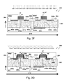
Next, as shown in FIG. 3G, a spacer layer sp is formed, and the N-type source 206 a is formed on the P-well 203 a in the epitaxial layer 202. The N-type source 206 a is located between the epitaxial top surface 202 a and the P-well 203 a in the vertical direction, and the N-type source 206 a connects the P-type body region 208 a and the PLDD region 205 a in the lateral direction. In the ion implantation process for forming the N-type source 206 a as shown in FIG. 3G, the ion implantation region can be defined by a mask including the spacer layer sp, the gate conductive layer st and the photoresist layer 206 a′. N-type impurities are implanted into the defined ion implantation region to form the N-type source 206 a. Preferably, the ion implantation can be performed with a tilt angle with respect to the epitaxial top surface 202 a as indicated by thinner dashed arrows shown in the figure, which is helpful in avoiding OFF-channel.
Next, as shown in FIG. 3H, a spacer layer sp′ is formed, and the P-type source 206 b is formed on the N-well 203 b in the epitaxial layer 202. The P-type source 206 b is located between the epitaxial top surface 202 a and the N-well 203 b in the vertical direction, and the P-type source 206 b connects the N-type body region 208 b and the NLDD region 205 c in the lateral direction. In the ion implantation process for forming the P-type source 206 b as shown in FIG. 3H, an ion implantation region can be defined by a mask including the spacer layer sp′, the gate conductive layer st′ and the photoresist layer 206 b′. P-type impurities are implanted into the defined ion implantation region to form the P-type source 206 b. Preferably, the ion implantation can be performed with a tilt angle with respect to the epitaxial top surface 202 a as indicated by thinner dashed arrows shown in the figure, which is helpful in avoiding OFF-channel.
Next, as shown in FIG. 3I, the P-type body region 208 a is formed on the P-type well 203 a in the epitaxial layer 202. The P-type body region 208 a is located between the P-well 203 a and the epitaxial top surface 202 a in the vertical direction. And, the N-type drain 207 a is formed on the N-well 203 c in the epitaxial layer 202. The N-type drain 207 a is located between the epitaxial top surface 202 a and the N-well 203 c in the vertical direction, and the N-type drain 207 a connects the NLDD region 205 b in the lateral direction. A PN junction 212 a is formed between the PLDD region 205 a and the NLDD region 205 b. In one embodiment, the ion implantation process for forming the N-type drain 207 a and the ion implantation process step for forming the N-type source 206 a can be integrated into one step.
Next, still referring to FIG. 3I, the N-type body region 208 b is formed on the N-well 203 b in the epitaxial layer 202. The N-type body region 208 b is located between the N-well 203 b and the epitaxial top surface 202 a in the vertical direction. And, the P-type drain 207 b is formed on the P-well 203 d in the epitaxial layer 202. The P-type drain 207 b is located between the epitaxial top surface 202 a and the P-well 203 d in the vertical direction, and the P-type drain 207 b connects the PLDD region 205 d in the lateral direction. A PN junction 212 b is formed between the NLDD region 205 c and the PLDD region 205 d. In one embodiment, the ion implantation process for forming the P-type drain 207 b and the ion implantation process step for forming the P-type source 206 b can be integrated into one step.
In one preferred embodiment, the PLDD region 205 a has an impurity concentration which is higher than an impurity concentration of the P-well 203 a, and the NLDD region 205 b has an impurity concentration which is higher than an impurity concentration of the N-well 203 c. For example, the impurity concentration of the PLDD region 205 a may be 2-10 folds of the impurity concentration of the P-well 203 a; the impurity concentration of the NLDD region 205 b may be 2-10 folds of the impurity concentration of the N-well 203 b. In one preferred embodiment, the NLDD region 205 c has an impurity concentration which is higher than an impurity concentration of the N-well 203 b, and the PLDD region 205 d has an impurity concentration which is higher than an impurity concentration of the N-well 203 d. For example, the impurity concentration of the NLDD region 205 c may be 2-10 folds of the impurity concentration of the N-well 203 b; the impurity concentration of the PLDD region 205 d may be 2-10 folds of the impurity concentration of the P-well 203 d. The impurity concentration described above refers to a planar dopant concentration parameter executed in an ion implantation process. Usually, after annealing process, a three-dimensional dopant concentration is formed and the three-dimensional dopant concentration is lower than the planar dopant concentration, as well-known by one skilled in the art. By the dopant concentration design in this embodiment, the HCE of the SCE can be alleviated.
FIG. 4 shows a dual-well CMOS device 300 according to a third embodiment of the present invention. This embodiment is different from the first embodiment in that the separation region 214 of the dual-well CMOS device 300 of this embodiment includes a P-type separation region 214 a and an N-type separation region 214 b. The P-type separation region 214 a is formed in the NMOS device region 204 a of the epitaxial layer 202. The P-type separation region 214 a upwardly connects the epitaxial top surface 202 a in the vertical direction, and the P-type separation region 214 a connects the N-well 203 c in the lateral direction. The N-type separation region 214 b is formed in the PMOS device region 204 b of the epitaxial layer 202. The N-type separation region 214 b upwardly connects the epitaxial top surface 202 a in the vertical direction, and the N-type separation region 214 b connects the P-well 203 d in the lateral direction. A depth of the separation region 214, which is measured from the epitaxial top surface 202 a downward, is not smaller than a depth of any of the P-well 203 a, the N-well 203 c, the N-well 203 b, and the P-well 203 d.
FIG. 5 shows a cross-section view of a dual-well CMOS device 400 according to a fourth embodiment of the present invention. This embodiment shows another option for forming the isolation region 204. As shown in FIG. 5, this embodiment is different from the first embodiment in that the isolation region 204 is formed by a shallow trench isolation (STI) process. Except the isolation region 204, the rest structure and manufacturing steps of the dual-well CMOS device 400 are the same as the first embodiment.
FIG. 6 shows a cross-section view of a dual-well CMOS device 500 according to a fifth embodiment of the present invention. This embodiment illustrates that, in a preferred embodiment of the present invention, the ion implantation process step for forming the N-type drain 207 a and the ion implantation process step for forming the N-type source 206 a can be integrated into one step. In this embodiment, the N-type impurities for forming the N-type drain 207 a are implanted with a tilt angle with respect to the epitaxial top surface 202 a, in the same process for forming the N-type source 206 a, such that some of the N-type impurities are implanted into the epitaxial layer 202 under the spacer layer sp as shown in FIG. 6. This arrangement can reduce the manufacturing cost because it does not require a separate individual step for forming the N-type drain 207 a. This embodiment also illustrates that, in a preferred embodiment of the present invention, the ion implantation process step for forming the P-type drain 207 b and the ion implantation process step for forming the P-type source 206 b can be integrated into one step. That is, the P-type impurities for forming the P-type drain 207 b are implanted with a tilt angle with respect to the epitaxial top surface 202 a, in the same process for forming the P-type source 206 b, such that some of the P-type impurities are implanted into the epitaxial layer 202 under the spacer layer sp′ as shown in FIG. 6. This arrangement can reduce the manufacturing cost because it does not require a separate individual step for forming the P-type drain 207 b.
The present invention is different from the prior art in many aspects. There are at least four differences between the dual-well CMOS device 200 of the present invention and the prior art MOS device 100 shown in FIG. 1, as follows:
1. The dual-well CMOS device 200 includes two wells having different conductive types from each other. The N-type source 206 a is on the P-well 203 a, and the P-well 203 a and the N-type source 206 a are at the same side of the PN junction 212 a. The N-type drain 207 a is on the N-well 203 c, and the N-well 203 c and the N-type drain 207 a are at the same side of the PN junction 212 a. The P-type source 206 a is on the N-well 203 b, and the N-well 203 b and the P-type source 206 a are at the same side of the PN junction 212 b. The P-type drain 207 b is on the P-well 203 d, and the P-well 203 d and the P-type drain 207 b are at the same side of the PN junction 212 b.
2. The dual-well CMOS device 200 includes two LDD regions having different conductive types from each other in each of the NMOS device region 204 a and the PMOS device region 204 b. The PLDD region 205 a and the P-well 203 a are at the same side of the PN junction 212 a. The NLDD region 205 b and the N-well 203 c are at the same side of the PN junction 212 a. The NLDD region 205 c and the N-well 203 b are at the same side of the PN junction 212 a. The PLDD region 205 d and the P-well 203 d are at the same side of the PN junction 212 b.
3. The dual-well CMOS device 200 includes the aforementioned PN junction 212 a, which is formed by the P-well 203 a and the N-well 203 c, and the aforementioned PN junction 212 b, which is formed by the P-well 203 d and the N-well 203 b. The PN junction 212 a is located between the PLDD region 205 a and the NLDD region 205 b. The PN junction 212 b is located between the PLDD region 205 d and the NLDD region 205 c.
4. The dual-well CMOS device 200 includes the separation region 214, which is connected between the PMOS device region 204 b and the NMOS device region 204 a, wherein the depth of the separation region 214, which is measured from the epitaxial top surface 202 a downward, is not smaller than the depth of any of the first P-well 203 a, the N-well 203 c, the N-well 203 b, and the P-well 203 d.
In the NMOS device region 104 a of the prior art CMOS device 100, when a bias voltage is applied to the gate 111 a, a channel is formed at the interface between the P-well 103 a and the dielectric layer of the gate 111 a (as shown by the dash square in FIG. 1) by attracting carriers. When the bias voltage changes, the number of the attracted carriers correspondingly changes, and the electrical field near the channel changes, whereby a current is generated and controlled, as well-known by one skilled in the art. However, in the NMOS device region 204 a of the dual-well CMOS device 200 of the present invention, the channel is defined by the N-type source 206 a and the P-well 203 a, which is different from the prior art CMOS device 100 in which the channel is defined by the NLDD region 105 a (same side as the N-type source 106 a) and the NLDD region 105 b (same side as the N-type drain 107 a). The channel of the NMOS device region 204 a of the dual-well CMOS device 200 is shown by the dash square in FIG. 2. To achieve the same electrical effect, the channel of the present invention is relatively shorter, so the conduction resistance through the channel is relatively lower. Besides, because the impurity concentration of the PLDD region 205 a is higher than the impurity concentration of the P-well 203 a, the SCE is suppressed. Further, in the prior art CMOS device 100, the breakdown occurs at the junction between the NLDD region 105 b and the P-well 103 a; because the impurity concentration of the NLDD region 105 b is relatively high, the breakdown voltage is correspondingly low. In the dual-well CMOS device 200 of the present invention, the breakdown occurs at the PN junction 212 a; because the impurity concentration of the N-well 203 c is relatively low, the breakdown voltage is correspondingly high, and the hot carrier effect is better suppressed. In the PMOS device region 204 b of the CMOS device 200 according to the present invention, the breakdown voltage is relatively higher than the prior art CMOS device 100, and the hot carrier effect is better suppressed than the prior art CMOS device 100 with the aforementioned reasons.
The present invention has been described in considerable detail with reference to certain preferred embodiments thereof. It should be understood that the description is for illustrative purpose, not for limiting the scope of the present invention. Those skilled in this art can readily conceive variations and modifications within the spirit of the present invention. For example, other process steps or structures which do not affect the primary characteristic of the device, such as a threshold voltage adjustment region, etc., can be added; for another example, the lithography step described in the above can be replaced by electron beam lithography or other lithography techniques. For another example, variations of one embodiment can be applied to other embodiments; for example, the separation region 214 which includes the P-type separation region 214 a and the N-type separation region 214 b shown in FIG. 4 can be adopted in the embodiments shown in FIGS. 5 and 6. In view of the foregoing, the spirit of the present invention should cover all such and other modifications and variations, which should be interpreted to fall within the scope of the following claims and their equivalents. An embodiment or a claim of the present invention does not need to achieve all the objectives or advantages of the present invention. The title and abstract are provided for assisting searches but not for limiting the scope of the present invention.

Claims (14)

What is claimed is:
1. A dual-well complementary metal oxide semiconductor (CMOS) device, comprising:
a substrate, including a top surface and a bottom surface opposite to the top surface in a vertical direction;
an epitaxial layer, which is formed on and connects at least a portion of the top surface of the substrate, the epitaxial layer including an epitaxial top surface opposite to the top surface in the vertical direction;
an isolation region, which is formed on the epitaxial layer, and configured to define an NMOS device region and a PMOS device region in the epitaxial layer;
a first P-type well (P-well), which is formed in the NMOS device region of the epitaxial layer and located under the epitaxial top surface in the vertical direction;
a P-type body region, which is formed on the first P-well in the epitaxial layer, and is located between the first P-well and the epitaxial top surface in the vertical direction;
a first N-type well (N-well), which is formed in the NMOS device region of the epitaxial layer and located under the epitaxial top surface in the vertical direction, and connects the first P-well in a lateral direction, to form a first PN junction between the first N-well and the first P-well;
a first gate, which is formed in the NMOS device region, and is stacked on and connects the epitaxial top surface in the vertical direction;
a first P-type lightly doped diffusion (PLDD) region, which is formed on the first P-well in the epitaxial layer, and is located between the epitaxial top surface and the first P-well in the vertical direction;
a first N-type lightly doped diffusion (NLDD) region, which is formed on the first N-well in the epitaxial layer, and is located between the epitaxial top surface and the first N-well in the vertical direction;
an N-type source, which is formed on the first P-well in the epitaxial layer, and is located between the epitaxial top surface and the first P-well in the vertical direction, wherein the N-type source connects the P-type body region and the first PLDD region in the lateral direction;
an N-type drain, which is formed on the first N-well in the epitaxial layer, and is located between the epitaxial top surface and the first N-well in the vertical direction, wherein the N-type drain connects the first NLDD region in the lateral direction;
a second N-type well (N-well), which is formed in the PMOS device region of the epitaxial layer and located under the epitaxial top surface in the vertical direction;
an N-type body region, which is formed on the second N-well in the epitaxial layer, and is located between the second N-well and the epitaxial top surface in the vertical direction;
a second P-type well (P-well), which is formed in the PMOS device region of the epitaxial layer and located under the epitaxial top surface in the vertical direction, and connects the second N-well in the lateral direction, to form a second PN junction between the second N-well and the second P-well;
a second gate, which is formed in the PMOS device region, and is stacked on and connects the epitaxial top surface in the vertical direction;
a second N-type lightly doped diffusion (NLDD) region, which is formed on the second N-well in the epitaxial layer, and is located between the epitaxial top surface and the second N-well in the vertical direction;
a second P-type lightly doped diffusion (PLDD) region, which is formed on the second P-well in the epitaxial layer, and is located between the epitaxial top surface and the second P-well in the vertical direction;
a P-type source, which is formed on the second N-well in the epitaxial layer, and is located between the epitaxial top surface and the second N-well in the vertical direction, wherein the P-type source connects the N-type body region and the second NLDD region in the lateral direction;
a P-type drain, which is formed on the second P-well in the epitaxial layer, and is located between the epitaxial top surface and the second P-well in the vertical direction, wherein the P-type drain connects the second PLDD region in the lateral direction; and
a separation region, which is connected between the PMOS device region and the NMOS device region, for separating the PMOS device region and the NMOS device region, wherein a depth of the separation region, which is measured from the epitaxial top surface downward, is not smaller than a depth of any of the first P-well, the first N-well, the second N-type well, and the second P-well;
wherein, the first PN junction is located between the first PLDD region and the first NLDD region;
wherein, the second PN junction is located between the second PLDD region and the second NLDD region.
2. The dual-well CMOS device of claim 1, wherein the isolation region includes a local oxidation of silicon (LOCOS) structure or a shallow trench isolation (STI) structure.
3. The dual-well CMOS device of claim 1, wherein an impurity concentration of the first PLDD region is higher than an impurity concentration of the first P-well, and an impurity concentration of the first NLDD region is higher than an impurity concentration of the first N-well.
4. The dual-well CMOS device of claim 1, wherein an impurity concentration of the second PLDD region is higher than an impurity concentration of the second P-well, and an impurity concentration of the second NLDD region is higher than an impurity concentration of the second N-well.
5. The dual-well CMOS device of claim 1, further comprising an N-type buried layer, which is formed at or around an interface between the substrate and the epitaxial layer, the N-type buried layer upwardly connecting the second P-well in the vertical direction.
6. The dual-well CMOS device of claim 1, wherein the separation region includes a deep trench isolation (DTI) structure.
7. The dual-well CMOS device of claim 1, wherein the separation region includes:
a P-type separation region, which is formed in the NMOS device region of the epitaxial layer, the P-type separation region upwardly connecting the epitaxial top surface in the vertical direction, and the P-type separation region laterally connecting the first N-well in the lateral direction; and
an N-type separation region, which is formed in the PMOS device region of the epitaxial layer, the N-type separation region upwardly connecting the epitaxial top surface in the vertical direction, and the N-type separation region laterally connecting the second P-well in the lateral direction.
8. A manufacturing method of a dual-well complementary metal oxide semiconductor (CMOS) device, comprising:
providing a substrate, which includes a top surface and a bottom surface opposite to the top surface in a vertical direction;
forming an epitaxial layer on and connecting at least a portion of the top surface of the substrate, the epitaxial layer including an epitaxial top surface opposite to the top surface in the vertical direction;
forming an isolation region on the epitaxial layer, to define an NMOS device region and a PMOS device region in the epitaxial layer;
forming a first P-type well (P-well) in the NMOS device region of the epitaxial layer, under the epitaxial top surface in the vertical direction;
forming a P-type body region on the first P-well in the epitaxial layer, between the first P-well and the epitaxial top surface in the vertical direction;
forming a first N-type well (N-well) in the NMOS device region of the epitaxial layer, under the epitaxial top surface in the vertical direction, wherein the first N-well connects the first P-well in a lateral direction, to form a first PN junction between the first N-well and the first P-well;
forming a first gate in the NMOS device region, wherein the first gate is stacked on and connects the epitaxial top surface in the vertical direction;
forming a first P-type lightly doped diffusion (PLDD) region on the first P-well in the epitaxial layer, between the epitaxial top surface and the first P-well in the vertical direction;
forming a first N-type lightly doped diffusion (NLDD) region on the first N-well in the epitaxial layer, between the epitaxial top surface and the first N-well in the vertical direction;
forming an N-type source on the first P-well in the epitaxial layer, between the epitaxial top surface and the first P-well in the vertical direction, wherein the N-type source connects the P-type body region and the first PLDD region in the lateral direction;
forming an N-type drain on the first N-well in the epitaxial layer, between the epitaxial top surface and the first N-well in the vertical direction, wherein the N-type drain connects the first NLDD region in the lateral direction;
forming a second N-type well (N-well) in the PMOS device region of the epitaxial layer, under the epitaxial top surface in the vertical direction;
forming an N-type body region on the second N-well in the epitaxial layer, between the second N-well and the epitaxial top surface in the vertical direction;
forming a second P-type well (P-well) in the PMOS device region of the epitaxial layer, under the epitaxial top surface in the vertical direction, wherein the second P-well connects the second N-well in a lateral direction, to form a second PN junction between the second N-well and the second P-well;
forming a second gate in the PMOS device region, wherein the second gate is stacked on and connects the epitaxial top surface in the vertical direction;
forming a second N-type lightly doped diffusion (NLDD) region on the second N-well in the epitaxial layer, between the epitaxial top surface and the second N-well in the vertical direction;
forming a second P-type lightly doped diffusion (PLDD) region on the second P-well in the epitaxial layer, between the epitaxial top surface and the second P-well in the vertical direction;
forming a P-type source on the second N-well in the epitaxial layer, between the epitaxial top surface and the second N-well in the vertical direction, wherein the P-type source connects the N-type body region and the second NLDD region in the lateral direction;
forming a P-type drain on the second P-well in the epitaxial layer, between the epitaxial top surface and the second P-well in the vertical direction, wherein the P-type drain connects the second PLDD region in the lateral direction; and
forming a separation region, which is connected between the PMOS device region and the NMOS device region, for separating the PMOS device region and the NMOS device region, wherein a depth of the separation region, which is measured from the epitaxial top surface downward, is not smaller than a depth of any of the first P-well, the first N-well, the second N-well, and the second P-well;
wherein, the first PN junction is located between the first PLDD region and the first NLDD region;
wherein, the second PN junction is located between the second PLDD region and the second NLDD region.
9. The manufacturing method of claim 8, wherein the isolation region includes a local oxidation of silicon (LOCOS) structure or a shallow trench isolation (STI) structure.
10. The manufacturing method of claim 8, wherein an impurity concentration of the first PLDD region is higher than an impurity concentration of the first P-well, and an impurity concentration of the first NLDD region is higher than an impurity concentration of the first N-well.
11. The manufacturing method of claim 8, wherein an impurity concentration of the second PLDD region is higher than an impurity concentration of the second P-well, and an impurity concentration of the second NLDD region is higher than an impurity concentration of the second N-well.
12. The manufacturing method of claim 8, further comprising: forming an N-type buried layer, which is formed at or around an interface between the substrate and the epitaxial layer, the N-type buried layer upwardly connecting the second P-well in the vertical direction.
13. The manufacturing method of claim 8, wherein the separation region includes a deep trench isolation (DTI) structure.
14. The manufacturing method of claim 8, wherein the separation region includes:
a P-type separation region, which is formed in the NMOS device region of the epitaxial layer, the P-type separation region upwardly connecting the epitaxial top surface in the vertical direction, and the P-type separation region laterally connecting the first N-well in the lateral direction; and
an N-type separation region, which is formed in the PMOS device region of the epitaxial layer, the N-type separation region upwardly connecting the epitaxial top surface in the vertical direction, and the N-type separation region laterally connecting the second P-well in the lateral direction.
US15/136,917 2016-02-02 2016-04-23 Complementary metal oxide semiconductor device with dual-well and manufacturing method thereof Active US9543303B1 (en)

Priority Applications (1)

Application Number Priority Date Filing Date Title
US15/136,917 US9543303B1 (en) 2016-02-02 2016-04-23 Complementary metal oxide semiconductor device with dual-well and manufacturing method thereof

Applications Claiming Priority (4)

Application Number Priority Date Filing Date Title
CN201610072078 2016-02-02
CN201610072078.3A CN107026199A (en) 2016-02-02 2016-02-02 Metal oxide semiconductor element with double wells and manufacturing method thereof
US15/066,207 US9525028B1 (en) 2016-02-02 2016-03-10 Dual-well metal oxide semiconductor (MOS) device and manufacturing method thereof
US15/136,917 US9543303B1 (en) 2016-02-02 2016-04-23 Complementary metal oxide semiconductor device with dual-well and manufacturing method thereof

Related Parent Applications (1)

Application Number Title Priority Date Filing Date
US15/066,207 Continuation-In-Part US9525028B1 (en) 2016-02-02 2016-03-10 Dual-well metal oxide semiconductor (MOS) device and manufacturing method thereof

Publications (1)

Publication Number Publication Date
US9543303B1 true US9543303B1 (en) 2017-01-10

Family

ID=57705834

Family Applications (1)

Application Number Title Priority Date Filing Date
US15/136,917 Active US9543303B1 (en) 2016-02-02 2016-04-23 Complementary metal oxide semiconductor device with dual-well and manufacturing method thereof

Country Status (1)

Country Link
US (1) US9543303B1 (en)

Cited By (2)

* Cited by examiner, † Cited by third party
Publication number Priority date Publication date Assignee Title
US20140227859A1 (en) * 2012-09-11 2014-08-14 Texas Instruments Incorporated Diffusion resistor with reduced voltage coefficient of resistance and increased breakdown voltage using cmos wells
TWI770401B (en) * 2019-03-07 2022-07-11 日商鎧俠股份有限公司 Semiconductor device and method of manufacturing the same

Citations (8)

* Cited by examiner, † Cited by third party
Publication number Priority date Publication date Assignee Title
US20050006701A1 (en) * 2003-07-07 2005-01-13 Tzu-Chiang Sung High voltage metal-oxide semiconductor device
US20060027874A1 (en) * 2004-08-03 2006-02-09 Taiwan Semiconductor Manufacturing Co., Ltd. Novel isolated LDMOS IC technology
US20060049452A1 (en) * 2004-09-07 2006-03-09 Taiwan Semiconductor Manufacturing Co., Ltd. Novel LDMOS IC technology with low threshold voltage
US20080237703A1 (en) * 2007-03-28 2008-10-02 Taiwan Semiconductor Manufacturing Co., Ltd. High voltage semiconductor devices and methods for fabricating the same
US7989889B1 (en) * 2008-06-17 2011-08-02 Rf Micro Devices, Inc. Integrated lateral high-voltage metal oxide semiconductor field effect transistor
US20110266620A1 (en) * 2009-11-02 2011-11-03 Vishay-Siliconix Transistor structure with feed-through source-to-substrate contact
US20130161750A1 (en) * 2011-12-23 2013-06-27 Katholieke Universiteit Leuven, K.U. Leuven R&D N-Channel Laterally Diffused Metal-Oxide-Semiconductor Device
US20140203358A1 (en) * 2013-01-23 2014-07-24 Freescale Semiconductor, Inc. Semiconductor device with enhanced 3d resurf

Patent Citations (8)

* Cited by examiner, † Cited by third party
Publication number Priority date Publication date Assignee Title
US20050006701A1 (en) * 2003-07-07 2005-01-13 Tzu-Chiang Sung High voltage metal-oxide semiconductor device
US20060027874A1 (en) * 2004-08-03 2006-02-09 Taiwan Semiconductor Manufacturing Co., Ltd. Novel isolated LDMOS IC technology
US20060049452A1 (en) * 2004-09-07 2006-03-09 Taiwan Semiconductor Manufacturing Co., Ltd. Novel LDMOS IC technology with low threshold voltage
US20080237703A1 (en) * 2007-03-28 2008-10-02 Taiwan Semiconductor Manufacturing Co., Ltd. High voltage semiconductor devices and methods for fabricating the same
US7989889B1 (en) * 2008-06-17 2011-08-02 Rf Micro Devices, Inc. Integrated lateral high-voltage metal oxide semiconductor field effect transistor
US20110266620A1 (en) * 2009-11-02 2011-11-03 Vishay-Siliconix Transistor structure with feed-through source-to-substrate contact
US20130161750A1 (en) * 2011-12-23 2013-06-27 Katholieke Universiteit Leuven, K.U. Leuven R&D N-Channel Laterally Diffused Metal-Oxide-Semiconductor Device
US20140203358A1 (en) * 2013-01-23 2014-07-24 Freescale Semiconductor, Inc. Semiconductor device with enhanced 3d resurf

Cited By (3)

* Cited by examiner, † Cited by third party
Publication number Priority date Publication date Assignee Title
US20140227859A1 (en) * 2012-09-11 2014-08-14 Texas Instruments Incorporated Diffusion resistor with reduced voltage coefficient of resistance and increased breakdown voltage using cmos wells
US10128145B2 (en) * 2012-09-11 2018-11-13 Texas Instruments Incorporated Diffusion resistor with reduced voltage coefficient of resistance and increased breakdown voltage using CMOS wells
TWI770401B (en) * 2019-03-07 2022-07-11 日商鎧俠股份有限公司 Semiconductor device and method of manufacturing the same

Similar Documents

Publication Publication Date Title
US8026549B2 (en) LDMOS with N-type isolation ring and method of fabricating the same
US8674442B2 (en) Semiconductor device and manufacturing method thereof
US9508845B1 (en) LDMOS device with high-potential-biased isolation ring
US11374124B2 (en) Protection of drain extended transistor field oxide
US10062704B2 (en) Buried-channel MOSFET and a surface-channel MOSFET of a same type and fabrication method thereof
CN113594251A (en) Power metal-oxide-semiconductor field effect transistor (MOSFET) and method of manufacturing the same
US20130313641A1 (en) Double diffused metal oxide semiconductor device
US9853099B1 (en) Double diffused metal oxide semiconductor device and manufacturing method thereof
US20140021545A1 (en) Pocket counterdoping for gate-edge diode leakage reduction
US9853100B1 (en) High voltage device and manufacturing method thereof
JP2014203851A (en) Semiconductor device and manufacturing method of the same
TWI605586B (en) Lateral double-diffused metal oxide semiconductor device and method of manufacturing same
US9583613B2 (en) Metal oxide semiconductor devices and fabrication methods
US20140199818A1 (en) Method for fabricating an esd protection device
US8828827B2 (en) Manufacturing method of anti punch-through leakage current metal-oxide-semiconductor transistor
CN108574014B (en) LDMOS device and manufacturing method thereof
US8723256B1 (en) Semiconductor device and fabricating method thereof
US9698257B2 (en) Symmetric LDMOS transistor including a well of a first type of conductivity and wells of an opposite second type of conductivity
US9543303B1 (en) Complementary metal oxide semiconductor device with dual-well and manufacturing method thereof
US9634139B1 (en) Dual-well metal oxide semiconductor (MOS) device and manufacturing method thereof
US9627524B2 (en) High voltage metal oxide semiconductor device and method for making same
US9525028B1 (en) Dual-well metal oxide semiconductor (MOS) device and manufacturing method thereof
TW201814904A (en) Double-diffused metal oxide semiconductor device and method of manufacturing same
US10438943B2 (en) Field-effect transistor and semiconductor device
US8912601B2 (en) Double diffused drain metal oxide semiconductor device and manufacturing method thereof

Legal Events

Date Code Title Description
AS Assignment

Owner name: RICHTEK TECHNOLOGY CORPORATION, TAIWAN

Free format text: ASSIGNMENT OF ASSIGNORS INTEREST;ASSIGNOR:HUANG, TSUNG-YI;REEL/FRAME:038362/0830

Effective date: 20160418

STCF Information on status: patent grant

Free format text: PATENTED CASE

MAFP Maintenance fee payment

Free format text: PAYMENT OF MAINTENANCE FEE, 4TH YEAR, LARGE ENTITY (ORIGINAL EVENT CODE: M1551); ENTITY STATUS OF PATENT OWNER: LARGE ENTITY

Year of fee payment: 4

MAFP Maintenance fee payment

Free format text: PAYMENT OF MAINTENANCE FEE, 8TH YEAR, LARGE ENTITY (ORIGINAL EVENT CODE: M1552); ENTITY STATUS OF PATENT OWNER: LARGE ENTITY

Year of fee payment: 8