US9542872B2 - Data driver for electrophoretic display - Google Patents
Data driver for electrophoretic display Download PDFInfo
- Publication number
- US9542872B2 US9542872B2 US13/842,600 US201313842600A US9542872B2 US 9542872 B2 US9542872 B2 US 9542872B2 US 201313842600 A US201313842600 A US 201313842600A US 9542872 B2 US9542872 B2 US 9542872B2
- Authority
- US
- United States
- Prior art keywords
- image data
- period
- sub
- multiplexer
- driver
- Prior art date
- Legal status (The legal status is an assumption and is not a legal conclusion. Google has not performed a legal analysis and makes no representation as to the accuracy of the status listed.)
- Active, expires
Links
- 239000003990 capacitor Substances 0.000 claims abstract description 66
- 230000001960 triggered effect Effects 0.000 claims description 3
- 238000010586 diagram Methods 0.000 description 12
- 238000004064 recycling Methods 0.000 description 2
- 238000000034 method Methods 0.000 description 1
- 238000012986 modification Methods 0.000 description 1
- 230000004048 modification Effects 0.000 description 1
- 238000002310 reflectometry Methods 0.000 description 1
- 238000004088 simulation Methods 0.000 description 1
Images


Classifications
-
- G—PHYSICS
- G09—EDUCATION; CRYPTOGRAPHY; DISPLAY; ADVERTISING; SEALS
- G09G—ARRANGEMENTS OR CIRCUITS FOR CONTROL OF INDICATING DEVICES USING STATIC MEANS TO PRESENT VARIABLE INFORMATION
- G09G3/00—Control arrangements or circuits, of interest only in connection with visual indicators other than cathode-ray tubes
- G09G3/20—Control arrangements or circuits, of interest only in connection with visual indicators other than cathode-ray tubes for presentation of an assembly of a number of characters, e.g. a page, by composing the assembly by combination of individual elements arranged in a matrix no fixed position being assigned to or needed to be assigned to the individual characters or partial characters
- G09G3/34—Control arrangements or circuits, of interest only in connection with visual indicators other than cathode-ray tubes for presentation of an assembly of a number of characters, e.g. a page, by composing the assembly by combination of individual elements arranged in a matrix no fixed position being assigned to or needed to be assigned to the individual characters or partial characters by control of light from an independent source
- G09G3/3433—Control arrangements or circuits, of interest only in connection with visual indicators other than cathode-ray tubes for presentation of an assembly of a number of characters, e.g. a page, by composing the assembly by combination of individual elements arranged in a matrix no fixed position being assigned to or needed to be assigned to the individual characters or partial characters by control of light from an independent source using light modulating elements actuated by an electric field and being other than liquid crystal devices and electrochromic devices
- G09G3/344—Control arrangements or circuits, of interest only in connection with visual indicators other than cathode-ray tubes for presentation of an assembly of a number of characters, e.g. a page, by composing the assembly by combination of individual elements arranged in a matrix no fixed position being assigned to or needed to be assigned to the individual characters or partial characters by control of light from an independent source using light modulating elements actuated by an electric field and being other than liquid crystal devices and electrochromic devices based on particles moving in a fluid or in a gas, e.g. electrophoretic devices
-
- G—PHYSICS
- G09—EDUCATION; CRYPTOGRAPHY; DISPLAY; ADVERTISING; SEALS
- G09G—ARRANGEMENTS OR CIRCUITS FOR CONTROL OF INDICATING DEVICES USING STATIC MEANS TO PRESENT VARIABLE INFORMATION
- G09G2310/00—Command of the display device
- G09G2310/02—Addressing, scanning or driving the display screen or processing steps related thereto
- G09G2310/0264—Details of driving circuits
- G09G2310/0275—Details of drivers for data electrodes, other than drivers for liquid crystal, plasma or OLED displays, not related to handling digital grey scale data or to communication of data to the pixels by means of a current
-
- G—PHYSICS
- G09—EDUCATION; CRYPTOGRAPHY; DISPLAY; ADVERTISING; SEALS
- G09G—ARRANGEMENTS OR CIRCUITS FOR CONTROL OF INDICATING DEVICES USING STATIC MEANS TO PRESENT VARIABLE INFORMATION
- G09G2310/00—Command of the display device
- G09G2310/06—Details of flat display driving waveforms
Definitions
- the disclosure relates in general to a data driver for an electrophoretic display (EPD), and more particularly to an EPD data driver having a charge recycling mechanism.
- EPD electrophoretic display
- EPDs electrophoretic displays
- a data driver for an electrophoretic display includes multiple driver sub-circuits, each of which drives a pixel column within a driving period via a driver end.
- Each of the driver sub-circuits includes an output node, first and second latches, first and second capacitors, a multiplexer and a comparator.
- the first and second latches respectively store updated latch image data and current latch image data in response to original image data.
- the second latch further provides the current latch image data to the output node.
- the updated and current latch image data selectively correspond to one of positive, negative and ground reference levels, respectively.
- the multiplexer is coupled to the first capacitor, the second capacitor, the output node and the driver end.
- the comparator divides the driving period into first, second and third periods.
- the comparator controls the multiplexer to selectively couple one of the first and second capacitors to the driver end in the first period, so as to recycle charges of the pixel column.
- the comparator further controls the multiplexer to selectively couple the other of the first and second capacitors to the driver end in the second period, so as to pre-charge the pixels with the charge.
- a data driver for an EPD includes multiple driver sub-circuits, each of which drives a pixel column within a driving period via a driver end.
- Each of the driver sub-circuits includes an output node, a ground power rail, first and second latches, first and second capacitors, a multiplexer and a comparator.
- the ground power rail provides a ground reference level.
- the first and second latches respectively store updated latch image data and current latch image data in response to original image data.
- the second latch further provides the current latch image data to the output node.
- the updated and current latch image data selectively correspond to one of positive, negative and ground reference levels, respectively.
- the multiplexer is coupled to the first capacitor, the second capacitor, the output node, the driver end and the ground power rail.
- the comparator divides the driving period into first to fourth periods. When the updated and current image data correspond to different levels, the comparator controls the multiplexer to selectively couple one of the first and second capacitors to the driver end in the first period, so as to recycle charges at the pixel column, and to selectively couple the other of the first and second capacitors to the driver end in the second period, so as to pre-charge the pixels with the charge.
- the comparator further controls the multiplexer to selectively couple the ground power rail to the driver end in the fourth period. The fourth period is triggered between the first and second periods.
- FIG. 2 is a detailed block diagram of a driver sub-circuit 10 ( i ) in FIG. 1 .
- FIG. 3 is a timing diagram of operations of the driver sub-circuit 10 ( i ).
- FIG. 4 is a table listing operations of a multiplexer 111 according to an embodiment of the present disclosure.
- FIG. 5 is another table listing operations of a multiplexer 111 according to an embodiment of the present disclosure.
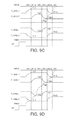
- FIGS. 6A to 6F are timing diagrams of associated signals in a driver sub-circuit 10 ( i )′.
- FIG. 7 is a detailed block diagram of the driver sub-circuit 10 ( i )′.
- FIG. 8 is a table listing operations of a multiplexer 111 ′ according to an embodiment of the present disclosure.
- FIGS. 9A to 9F are timing diagrams of associated signals in a driver sub-circuit 10 ( i )′′.
- FIG. 10 is a detailed block diagram of the driver sub-circuit 10 ( i )′′.
- a data driver for an electrophoretic display is provided by the embodiments below. Through time-division multiplexing, positive and negative charges at pixel columns is recycled.
- FIG. 1 shows a block diagram of an EPD according to an embodiment of the present disclosure.
- an EPD 1 includes a data driver 10 and an EPD panel 20 .
- the EPD panel 20 has a pixel array including m*n pixels, where m and n are natural numbers greater than 1. Further, structure of the EPD panel 20 according to the embodiment is not defined here, and associated details are omitted herein.
- equivalent resistance Rload and equivalent capacitance Cload of n pixels columns in the EPD panel 20 are depicted in representation.
- the data driver 10 includes first and second latches 10 _ 1 and 10 _ 3 , a level shifter 10 _ 5 , an output buffer 10 _ 7 , a comparator 10 _ 9 and a multiplexer 10 _ 11 .
- each of the foregoing circuits correspondingly includes n units.
- the n units correspondingly form n driver sub-circuits 10 ( 1 ), 10 ( 2 ), . . . , and 10 ( n ), each of which including n driver ends N 1 , N 2 , . . . , and Nn for respectively driving n pixel columns in the pixel array.
- the data driver 10 further includes capacitors Cpos and Cneg for respectively storing recycled charges at the pixels of the n pixel columns.
- capacitors Cpos and Cneg for respectively storing recycled charges at the pixels of the n pixel columns.
- an i th driver sub-circuit is taken as an example for illustrating details of operations of the n driver sub-circuits of the data driver 10 according to the embodiment, where i is a natural number small than or equal to n.
- FIG. 2 shows a detailed block diagram of a driver sub-circuit 10 ( i ) in FIG. 1 .
- the driver sub-circuit 10 ( i ) includes a latch 101 , a latch 103 , a level shifter 105 , an output buffer 107 , a comparator 109 , a multiplexer 111 and an output node Nd.
- Latch image data Vin_L′ and Vin_L may be respectively regarded as frame data of original image data Vin corresponding to different time points.
- the latch 101 receives the original image data Vin, and writes the updated latch image data Vin_L corresponding to a current timing period in response to a load control signal HSP provided by an external timing controller.
- the latch 103 writes the current latch image data Vin_L′ in response to a falling edge of a load control signal LD provided by the external timing controller.
- the current and updated latch image data are image data of (s ⁇ 1) th and 5 th frames in the original image data Vin, where s is a natural number.
- the level shifter 105 and the output buffer 107 further correspondingly perform corresponding operations on the current latch image data Vin_L′ to provide a driving signal Vd to the output node Nd.
- the original image data Vin, the current latch image data Vin_L′ and the updated latch image data Vin_L selectively correspond to one of positive, negative and ground reference levels VPOS, VNEG and GND, respectively.
- the corresponding driving signal Vd selectively corresponds to one of three levels +15V, ⁇ 15V and GND.
- the multiplexer 109 has four inputs and an output.
- the inputs of the multiplexer 109 are respectively coupled to the capacitors Cpos and Cneg, the ground power rail 113 and the output node Nd.
- the output of the multiplexer 109 is coupled to the driver end Ni.
- the comparator 109 divides the driving period TP into periods W1, W2, W3 and W4, as shown in FIG. 4 . Based on levels of the current and updated latch image data Vin_L′ and Vin_L, the comparator 109 provides a control signal IC in the periods W1 to W4 to switch the multiplexer 111 , thereby performing a time-division multiplexing operation on the i th pixel column.
- the driver sub-circuit 10 ( i ) drives and switches the level of the driving signal Vd.
- the comparator 109 controls the multiplexer 111 to selectively couple one of the capacitors Cpos and Cneg to the driver end Ni in the period W1, so as to recycle charges at the i th pixel column.
- the comparator 109 controls the multiplexer 111 to selectively couple the other of the capacitors Cpos and Cneg to the driver end Ni in the period W2, so as to pre-charge the i th pixel column by the recycled charges.
- the comparator 109 further controls the multiplexer 111 to couple the output node Ni to the driver end Nd in the period W3, so as to drive the i th pixel column.
- FIG. 4 shows a table of listing operations of the multiplexer 111 according to an embodiment of the present disclosure. Several operation examples are described below for further explaining switching operations of the multiplexer 111 in the periods W1 to W4.
- the comparator 109 controls the multiplexer 111 to couple the capacitor Cpos to the driver end in the period W1, so as to recycle and store the positive charges at the i th pixel column to the capacitor Cpos.
- the comparator 109 controls the multiplexer 111 to couple the capacitor Cpos to the driver end Ni in the period W2, so as to pre-charge the i th pixel column with positive charges stored in the capacitor Cpos.
- the comparator 109 controls the multiplexer 111 to couple the capacitor Cneg to the driver end Ni in the period W1, so as to recycle and store negative charges at the i th pixel column to the capacitor Cneg.
- the comparator 109 controls the multiplexer 111 to couple the capacitor Cneg to the driver end Ni in the period W2, so as to pre-discharge the i th pixel column with negative charges stored in the capacitor Cneg.
- the comparator 109 controls the multiplexer 111 to couple the ground power rail 113 to the driver end Ni in the period W1. Also refer to operation examples numbered #1 to #3 in FIG. 4 .
- the comparator 109 controls the multiplexer 111 to couple the ground power rail 113 to the driver end Ni in the period W2.
- the comparator 109 controls the multiplexer 111 to couple the output node Nd to the ground power rail 113 in the periods W1 and W2.
- the comparator 109 controls the multiplexer 111 to couple the output node Nd to the driver end Ni in the periods W1 and W2.
- the comparator 109 controls the multiplexer 111 to couple the output node Nd to the driver end Ni in the periods W1 and W2.
- the driver sub-circuit 10 ( i ) is capable of recycling and storing positive and negative charges at the i th pixel column to the capacitors Cpos and Cneg in the period W1, and reuses the positive and negative charges in the capacitors Cpos and Cneg in the period W2.
- the driver sub-circuit 10 ( i ) according to the embodiment further couples the output node Nd to the driver end Ni in the period W3, i.e., after the charges are fed back and recycled, so that the driver sub-circuit 10 ( i ) drives the i th pixel column.
- the period W4 is triggered between the periods W1 and W2.
- the comparator 109 controls the multiplexer 111 to selectively couple the ground power rail 113 to the driver end Ni in the period W4.
- the comparator 109 controls the multiplexer 111 to couple the ground power rail 113 to the driver end Ni in the period W4, so as to correspondingly provide the ground reference voltage to the i th pixel column.
- the comparator 109 controls the multiplexer 111 to couple the output node Nd to the driver end Ni in the period W4.
- the comparator 109 controls the multiplexer 111 to couple the output node Nd to the driver end Ni in the period W4.
- situations of the driving period TP divided into four periods W1 to W4 are taken as examples, and are not to be construed as limitations of the data driver 10 of the present disclosure.
- the comparator 109 may also omit the period W4 and complete driving operations in the three periods W1 to W3, as shown in FIG. 5 .
- a capacitor Cpos′ includes two or more sub-capacitors Cpos_ 1 , Cpos_ 2 , . . . and Cpos_k
- a capacitor Cneg′ includes two or more sub-capacitors Cneg_ 1 , Cneg_ 2 , . . . and Cneg_k, where k is a natural number greater than 1, as shown in FIG. 7 .
- a multiplexer 111 ′ correspondingly has 2k+2 inputs respectively coupled to k sub-capators Cpos_ 1 to Cpos_ki, k sub-capacitors Cneg_ 1 to Cneg_k, the output node Nd and a ground power rail 113 ′.
- the comparator 109 may further respectively divide the periods W1 and W2 into k sub-periods W1_1 to W1_k and k sub-periods W2_1 to W2_k, as shown in FIG. 8 .
- the comparator 109 ′ respectively couples the corresponding sub-capacitors Cpos_ 1 to Cpos_k or the sub-capacitors Cneg_ 1 to Cneg_k to the driver end Ni, so as to recycle and store the positive charges at the i th pixel column to the sub-capacitors Cpos_ 1 to Cpos_k, and to recycle and store the negative charges at the i th pixel column to the sub-capacitors Cneg_ 1 to Cneg_k.
- the comparator 109 ′ respectively couples the corresponding sub-capacitors Cpos_ 1 to Cpos_k or the sub-capacitors Cneg_ 1 to Cneg_k to the driver end Ni, so as to provide the recycled and stored positive and negative charges to the i th pixel column for pre-charge or pre-discharge.
- the driver sub-circuit 10 ( i )′ of the embodiment may recycle and reuse charges at the i th pixel column.
- FIGS. 9A to 9F show timing diagrams of associated signals in the driver sub-circuit 10 ( i )′ in FIG. 7 . Taking k equal to 2 for example, waveforms of associated signals in operation examples numbered #2 to #4 and #6 to #8 in FIG. 8 are as respectively shown in FIGS. 9A to 9F .
- FIG. 10 shows a detailed block diagram of the driver sub-circuit 10 ( i )′′; and FIGS. 6A to 6F show timing diagrams of associated signals in the driver sub-circuit 10 ( i )′′.
- the operation examples in FIGS. 9A to 9F may also omit the period W4, with the operation period TP being divided to only periods W1_1, W1_2, W2_1, W2_2 and W3, in which corresponding driving operations are performed.
Landscapes
- Engineering & Computer Science (AREA)
- Physics & Mathematics (AREA)
- Computer Hardware Design (AREA)
- General Physics & Mathematics (AREA)
- Theoretical Computer Science (AREA)
- Control Of Indicators Other Than Cathode Ray Tubes (AREA)
Abstract
A data driver for an electrophoretic display (EPD) includes multiple driver sub-circuits. Each of the driver sub-circuits includes first and second latches, first and second capacitors, a multiplexer and a comparator. The first and second latches respectively provide updated latch image data and current latch image data in response to original image data. When the updated and current latch image data correspond to different levels, the comparator controls the multiplexer in a first period to selectively couple one of the first and second capacitors to a driver end, so as to recycle charges at pixels, and controls the multiplexer in a second period to selectively couple the other of the first and second capacitors to the driver end to pre-charge the pixels with the charges.
Description
This application claims the benefit of Taiwan application Serial No. 101123083, filed Jun. 27, 2012, the subject matter of which is incorporated herein by reference.
The disclosure relates in general to a data driver for an electrophoretic display (EPD), and more particularly to an EPD data driver having a charge recycling mechanism.
In a modern world with ever-progressing technology, display-associated techniques such as electrophoretic displays (EPDs) are developed for providing convenience in the daily life. In general, an EPD, featuring high reflectivity, high contrast and capability of sustaining stable images, is common in electronic books to provide users with simulation of ordinary ink on conventional paper. Therefore, researchers and developers of the industry constantly seek for a display driving mechanism with enhanced power efficiency for an EPD.
According to an example the present disclosure, a data driver for an electrophoretic display (EPD) is provided. The data driver includes multiple driver sub-circuits, each of which drives a pixel column within a driving period via a driver end. Each of the driver sub-circuits includes an output node, first and second latches, first and second capacitors, a multiplexer and a comparator. The first and second latches respectively store updated latch image data and current latch image data in response to original image data. The second latch further provides the current latch image data to the output node. The updated and current latch image data selectively correspond to one of positive, negative and ground reference levels, respectively. The multiplexer is coupled to the first capacitor, the second capacitor, the output node and the driver end. The comparator divides the driving period into first, second and third periods. When the updated and current image data correspond to different levels, the comparator controls the multiplexer to selectively couple one of the first and second capacitors to the driver end in the first period, so as to recycle charges of the pixel column. The comparator further controls the multiplexer to selectively couple the other of the first and second capacitors to the driver end in the second period, so as to pre-charge the pixels with the charge.
According to another example of the present disclosure, a data driver for an EPD is provided. The data driver includes multiple driver sub-circuits, each of which drives a pixel column within a driving period via a driver end. Each of the driver sub-circuits includes an output node, a ground power rail, first and second latches, first and second capacitors, a multiplexer and a comparator. The ground power rail provides a ground reference level. The first and second latches respectively store updated latch image data and current latch image data in response to original image data. The second latch further provides the current latch image data to the output node. The updated and current latch image data selectively correspond to one of positive, negative and ground reference levels, respectively. The multiplexer is coupled to the first capacitor, the second capacitor, the output node, the driver end and the ground power rail. The comparator divides the driving period into first to fourth periods. When the updated and current image data correspond to different levels, the comparator controls the multiplexer to selectively couple one of the first and second capacitors to the driver end in the first period, so as to recycle charges at the pixel column, and to selectively couple the other of the first and second capacitors to the driver end in the second period, so as to pre-charge the pixels with the charge. The comparator further controls the multiplexer to selectively couple the ground power rail to the driver end in the fourth period. The fourth period is triggered between the first and second periods.
The above and other contents of the disclosure will become better understood with regard to the following detailed description of the preferred but non-limiting embodiments. The following description is made with reference to the accompanying drawings.
In the following detailed description, for purposes of explanation, numerous specific details are set forth in order to provide a thorough understanding of the disclosed embodiments. It will be apparent, however, that one or more embodiments may be practiced without these specific details.
In other instances, well-known structures and devices are schematically shown in order to simplify the drawing.
A data driver for an electrophoretic display (EPD) is provided by the embodiments below. Through time-division multiplexing, positive and negative charges at pixel columns is recycled.
The data driver 10 includes first and second latches 10_1 and 10_3, a level shifter 10_5, an output buffer 10_7, a comparator 10_9 and a multiplexer 10_11. For example, each of the foregoing circuits correspondingly includes n units. The n units correspondingly form n driver sub-circuits 10(1), 10(2), . . . , and 10(n), each of which including n driver ends N1, N2, . . . , and Nn for respectively driving n pixel columns in the pixel array.
The data driver 10 further includes capacitors Cpos and Cneg for respectively storing recycled charges at the pixels of the n pixel columns. As the driver sub-circuits have a substantially same circuit structure, an ith driver sub-circuit is taken as an example for illustrating details of operations of the n driver sub-circuits of the data driver 10 according to the embodiment, where i is a natural number small than or equal to n.
Latch image data Vin_L′ and Vin_L may be respectively regarded as frame data of original image data Vin corresponding to different time points. The latch 101 receives the original image data Vin, and writes the updated latch image data Vin_L corresponding to a current timing period in response to a load control signal HSP provided by an external timing controller. The latch 103 writes the current latch image data Vin_L′ in response to a falling edge of a load control signal LD provided by the external timing controller. For example, the current and updated latch image data are image data of (s−1)th and 5th frames in the original image data Vin, where s is a natural number.
The level shifter 105 and the output buffer 107 further correspondingly perform corresponding operations on the current latch image data Vin_L′ to provide a driving signal Vd to the output node Nd. For example, the original image data Vin, the current latch image data Vin_L′ and the updated latch image data Vin_L selectively correspond to one of positive, negative and ground reference levels VPOS, VNEG and GND, respectively. The corresponding driving signal Vd selectively corresponds to one of three levels +15V, −15V and GND.
For example, the multiplexer 109 has four inputs and an output. The inputs of the multiplexer 109 are respectively coupled to the capacitors Cpos and Cneg, the ground power rail 113 and the output node Nd. The output of the multiplexer 109 is coupled to the driver end Ni.
The comparator 109 divides the driving period TP into periods W1, W2, W3 and W4, as shown in FIG. 4 . Based on levels of the current and updated latch image data Vin_L′ and Vin_L, the comparator 109 provides a control signal IC in the periods W1 to W4 to switch the multiplexer 111, thereby performing a time-division multiplexing operation on the ith pixel column. When the current and updated latch image data Vin_L′ and Vin_L correspond to different levels, the driver sub-circuit 10(i) drives and switches the level of the driving signal Vd.
Accordingly, the comparator 109 controls the multiplexer 111 to selectively couple one of the capacitors Cpos and Cneg to the driver end Ni in the period W1, so as to recycle charges at the ith pixel column. The comparator 109 controls the multiplexer 111 to selectively couple the other of the capacitors Cpos and Cneg to the driver end Ni in the period W2, so as to pre-charge the ith pixel column by the recycled charges. The comparator 109 further controls the multiplexer 111 to couple the output node Ni to the driver end Nd in the period W3, so as to drive the ith pixel column. Thus, power consumption by the driver sub-circuit 10(i) may be effectively reduced by the foregoing switching operation on the multiplexer 111.
Referring to operation examples numbered #2 and #8 in FIG. 4 , when the current latch image data Vin_L′ correspond to the positive reference level VPOS, and the current and updated latch image data Vin_L′ and Vin_L have different levels, it means that a start level of the driving signal Vd is the positive reference level VPOS, and an end level of the driving signal Vd is one of the negative reference level VNEG and the ground reference level GND. Accordingly, the comparator 109 controls the multiplexer 111 to couple the capacitor Cpos to the driver end in the period W1, so as to recycle and store the positive charges at the ith pixel column to the capacitor Cpos.
Referring to operation examples numbered #4 and #6 in FIG. 4 , when the updated latch image data Vin_L correspond to the positive reference level VPOS, and the current and updated latch image data Vin_L′ and Vin_L correspond to different levels, it means that the end level of the driving signal Vd is the positive reference level VPOS, and the start level is one of the negative reference level VENG and the ground reference level GND. Accordingly, the comparator 109 controls the multiplexer 111 to couple the capacitor Cpos to the driver end Ni in the period W2, so as to pre-charge the ith pixel column with positive charges stored in the capacitor Cpos.
Referring to operation examples numbered #3 and #6 in FIG. 4 , when the current latch image data Vin_L′ correspond to the negative reference level VNEG, and the current and updated latch image data Vin_L′ and Vin_L correspond to different levels, it means that the start level of the driving signal Vd is the negative reference level VNEG, and the end level of the driving signal Vd is one of the positive reference level VPOS and the ground reference level GND. Accordingly, the comparator 109 controls the multiplexer 111 to couple the capacitor Cneg to the driver end Ni in the period W1, so as to recycle and store negative charges at the ith pixel column to the capacitor Cneg.
Referring to operation examples numbered #7 and #8 in FIG. 4 , when the updated latch image data Vin_L correspond to the negative reference level VNEG, and the current and updated latch image data Vin_L′ and Vin_L correspond to different levels, it means that the end level of the driving signal Vd is the negative reference level VNEG, and the start level of the driving signal Vd is one of the positive reference level VPOS and the ground reference level GND. Accordingly, the comparator 109 controls the multiplexer 111 to couple the capacitor Cneg to the driver end Ni in the period W2, so as to pre-discharge the ith pixel column with negative charges stored in the capacitor Cneg.
Referring to the operation examples numbered #4 and #7 in FIG. 4 , when the current latch image data Vin_L′ correspond to the ground reference level GND, it means that the start level of the driving signal Vd is the ground reference level GND. Accordingly, the comparator 109 controls the multiplexer 111 to couple the ground power rail 113 to the driver end Ni in the period W1. Also refer to operation examples numbered #1 to #3 in FIG. 4 .
Referring to the operation examples numbered #2 and #3 in FIG. 4 , when the updated latch image data Vin_L correspond to the ground reference level GND, it means that the end level of the driving signal Vd is the ground reference level GND. Accordingly, the comparator 109 controls the multiplexer 111 to couple the ground power rail 113 to the driver end Ni in the period W2.
Referring to the operation example numbered #1 in FIG. 4 , when the current and updated latch image data Vin_L′ and Vin_L both correspond to the ground reference level GND, it means that the driving signal Vd is not to be switched, and sustains at the fixed level. Accordingly, the comparator 109 controls the multiplexer 111 to couple the output node Nd to the ground power rail 113 in the periods W1 and W2.
Referring to the operation examples number # 5 and #9 in FIG. 4 , when the current and updated latch image data Vin_L′ and Vin_L both correspond to the positive reference level VPOS, it means that the driving signal Vd is not to be switched, and the driver sub-circuit 10(i) is not required to drive the ith pixel column in the driving period TP. Accordingly, the comparator 109 controls the multiplexer 111 to couple the output node Nd to the driver end Ni in the periods W1 and W2. Similarly, when the current and updated latch image data Vin_L′ and Vin_L both correspond to the negative reference level VNEG, the comparator 109 controls the multiplexer 111 to couple the output node Nd to the driver end Ni in the periods W1 and W2.
In conclusion, the driver sub-circuit 10(i) according to the embodiment is capable of recycling and storing positive and negative charges at the ith pixel column to the capacitors Cpos and Cneg in the period W1, and reuses the positive and negative charges in the capacitors Cpos and Cneg in the period W2. The driver sub-circuit 10(i) according to the embodiment further couples the output node Nd to the driver end Ni in the period W3, i.e., after the charges are fed back and recycled, so that the driver sub-circuit 10(i) drives the ith pixel column.
The period W4 is triggered between the periods W1 and W2. The comparator 109 controls the multiplexer 111 to selectively couple the ground power rail 113 to the driver end Ni in the period W4.
Referring to the operation examples numbered #1 to #4 and #6 to #8 in FIG. 4 , when the current and updated latch image data Vin_L′ and Vin_L do not both correspond to the positive reference level VPOS (i.e., other operation examples except the operation example #5), or do not both correspond to the negative reference level VNEG (i.e., other operation examples except the operation example #9), the comparator 109 controls the multiplexer 111 to couple the ground power rail 113 to the driver end Ni in the period W4, so as to correspondingly provide the ground reference voltage to the ith pixel column.
Referring to the operation examples numbered #5 and #9 in FIG. 4 , when the current and updated latch image data Vin_L′ and Vin_L both correspond to the positive reference level VPOS, the comparator 109 controls the multiplexer 111 to couple the output node Nd to the driver end Ni in the period W4. When the current and updated latch image data Vin_L′ and Vin_L both correspond to the negative reference level VNEG, the comparator 109 controls the multiplexer 111 to couple the output node Nd to the driver end Ni in the period W4.
In this embodiment, situations of the driving period TP divided into four periods W1 to W4 are taken as examples, and are not to be construed as limitations of the data driver 10 of the present disclosure. In another embodiment, the comparator 109 may also omit the period W4 and complete driving operations in the three periods W1 to W3, as shown in FIG. 5 .
In another embodiment, for example, a capacitor Cpos′ includes two or more sub-capacitors Cpos_1, Cpos_2, . . . and Cpos_k, and a capacitor Cneg′ includes two or more sub-capacitors Cneg_1, Cneg_2, . . . and Cneg_k, where k is a natural number greater than 1, as shown in FIG. 7 .
In the embodiment shown in FIG. 7 , a multiplexer 111′ correspondingly has 2k+2 inputs respectively coupled to k sub-capators Cpos_1 to Cpos_ki, k sub-capacitors Cneg_1 to Cneg_k, the output node Nd and a ground power rail 113′. Moreover, the comparator 109 may further respectively divide the periods W1 and W2 into k sub-periods W1_1 to W1_k and k sub-periods W2_1 to W2_k, as shown in FIG. 8 .
In each of the k sub-periods W1_1 to W1_k, the comparator 109′ respectively couples the corresponding sub-capacitors Cpos_1 to Cpos_k or the sub-capacitors Cneg_1 to Cneg_k to the driver end Ni, so as to recycle and store the positive charges at the ith pixel column to the sub-capacitors Cpos_1 to Cpos_k, and to recycle and store the negative charges at the ith pixel column to the sub-capacitors Cneg_1 to Cneg_k. In the k sub-periods W2_1 to W2_k, the comparator 109′ respectively couples the corresponding sub-capacitors Cpos_1 to Cpos_k or the sub-capacitors Cneg_1 to Cneg_k to the driver end Ni, so as to provide the recycled and stored positive and negative charges to the ith pixel column for pre-charge or pre-discharge.
Thus, through the switching operations of the sub-periods W1_1 to W1_k and W2_1 to W2_k, the driver sub-circuit 10(i)′ of the embodiment may recycle and reuse charges at the ith pixel column.
It will be apparent to those skilled in the art that various modifications and variations can be made to the disclosed embodiments. It is intended that the specification and examples be considered as exemplary only, with a true scope of the disclosure being indicated by the following claims and their equivalents.
Claims (12)
1. A data driver for an electrophoretic display (EPD), comprising a plurality of driver sub-circuits, each of the driver sub-circuits driving a pixel column of the EPD in a driving period via a driver end; wherein each of the driver sub-circuits comprises:
an output node;
a first latch and a second latch, for respectively storing updated latch image data and current latch image data in response to original image data, the second latch further providing the current latch image data to the output node, the updated latch image data and the current latch image data each selectively corresponding individually to one of a positive reference level, a negative reference level and a ground reference level;
a multiplexer, coupled to a first capacitor, a second capacitor, the output node and the driver end; and
a comparator, dividing the driving period into a first period, a second period and a third period, wherein when the updated latch image data and the current latch image data selectively correspond to different levels, the comparator controls the multiplexer to selectively couple one of the first and second capacitors to the driver end in the first period to recycle charges at the pixel column into the coupled one of the first and second capacitors, and to selectively couple said one of the first and second capacitors to the driver end in the second period to pre-charge or pre-discharge the pixel column with the recycled charges in the coupled one of the first and second capacitors,
wherein when the current latch image data correspond to the positive reference level, and the updated and current latch image data correspond to different levels, the comparator controls the multiplexer to couple the first capacitor to the driver end in the first period to recycle positive charges at the pixel column to the first capacitor.
2. The data driver according to claim 1 , wherein when the updated latch image data correspond to the positive reference level, and the updated and current latch image data correspond to different reference levels, the comparator controls the multiplexer to couple the first capacitor to the driver end in the second period to precharge the pixel column with the positive charges in the first capacitor.
3. The data driver according to claim 2 , wherein
the first capacitor comprises a plurality of sub-capacitors, and the multiplexer correspondingly comprises a plurality of inputs respectively coupled to the sub-capacitors;
the comparator correspondingly divides the first period into a plurality of first sub-periods, and respectively conducts the sub-capacitors in the first sub-periods to recycle the positive charges to the sub-capacitors; and
the comparator correspondingly divides the second period into a plurality of second sub-periods, and respectively conducts the sub-capacitors in the second sub-periods to pre-charge the pixel column with the positive charges in the sub-capacitors.
4. The data driver according to claim 1 , wherein when the current latch image data correspond to the negative reference level, and the updated and current latch image data correspond to different levels, the comparator controls the multiplexer to couple the second capacitor to the driver end in the first period to recycle negative charges at the pixel column to the second capacitor.
5. The data driver according to claim 4 , wherein when the updated latch image data correspond to the negative reference level, and the updated and current latch image data correspond to different levels, the comparator controls the multiplexer to couple the second capacitor to the driver end in the second period to pre-discharge the pixel column with the negative charges in the second capacitor.
6. The data driver according to claim 5 , wherein
the second capacitor comprises a plurality of sub-capacitors, and the multiplexer correspondingly comprises a plurality of inputs respectively coupled to the sub-capacitors;
the comparator correspondingly divides the first period into a plurality of first sub-periods, and respectively conducts the sub-capacitors in the first sub-periods to recycle the negative charges to the sub-capacitors; and
the comparator correspondingly divides the second period into a plurality of second sub-periods, and respectively conducts the sub-capacitors in the second sub-periods to pre-discharge the pixel column with the negative charges in the sub-capacitors.
7. The data driver according to claim 1 , wherein the multiplexer is further coupled to a ground power rail providing the ground reference level.
8. The data driver according to claim 7 , wherein
when the current latch image data correspond to the ground reference level, the comparator controls the multiplexer to couple the ground power rail to the driver end in the first period; and
when the updated latch image data correspond to the ground reference level, the comparator controls the multiplexer to couple the ground power rail to the driver end in the second period.
9. The data driver according to claim 7 , wherein the comparator further divides a fourth period in the driving period, and controls the multiplexer to selectively couple the ground power rail to the driver end in the fourth period, the fourth period triggered between the first and second periods.
10. The data driver according to claim 9 , wherein
when the updated and current latch image data do not both correspond to the positive reference level, the comparator controls the multiplexer to couple the ground power rail to the driver end in the fourth period; and
when the updated and current latch image data do not both correspond to the negative reference level, the comparator controls the multiplexer to couple the ground power rail to the driver end in the fourth period.
11. The data driver according to claim 1 , wherein
when the updated and current latch image data both correspond to the positive reference level, the comparator controls the multiplexer to couple the output node to the driver end in the first and second periods; and
when the updated and current latch image data both correspond to the negative reference level, the comparator controls the multiplexer to couple the output node to the driver end in the first and second periods.
12. The data driver according to claim 1 , wherein the comparator further controls the multiplexer to couple the output node to the driver end in the third period to drive the pixel column.
Applications Claiming Priority (3)
| Application Number | Priority Date | Filing Date | Title |
|---|---|---|---|
| TW101123083A | 2012-06-27 | ||
| TW101123083A TWI455095B (en) | 2012-06-27 | 2012-06-27 | Data driver for electrophoretic display |
| TW101123083 | 2012-06-27 |
Publications (2)
| Publication Number | Publication Date |
|---|---|
| US20140002435A1 US20140002435A1 (en) | 2014-01-02 |
| US9542872B2 true US9542872B2 (en) | 2017-01-10 |
Family
ID=49777635
Family Applications (1)
| Application Number | Title | Priority Date | Filing Date |
|---|---|---|---|
| US13/842,600 Active 2033-12-24 US9542872B2 (en) | 2012-06-27 | 2013-03-15 | Data driver for electrophoretic display |
Country Status (2)
| Country | Link |
|---|---|
| US (1) | US9542872B2 (en) |
| TW (1) | TWI455095B (en) |
Cited By (2)
| Publication number | Priority date | Publication date | Assignee | Title |
|---|---|---|---|---|
| US10692456B2 (en) * | 2018-08-02 | 2020-06-23 | Samsung Electronics Co., Ltd. | Display driver and output buffer |
| US20250149004A1 (en) * | 2023-11-08 | 2025-05-08 | E Ink Holdings Inc. | Display device and operating method for display device |
Families Citing this family (5)
| Publication number | Priority date | Publication date | Assignee | Title |
|---|---|---|---|---|
| KR102105410B1 (en) * | 2013-07-25 | 2020-04-29 | 삼성전자주식회사 | Display driver ic, apparatus including the same, and operation method thereof |
| KR102315421B1 (en) | 2015-03-30 | 2021-10-22 | 삼성디스플레이 주식회사 | Demultiplexer and display device including the same |
| KR102318144B1 (en) | 2015-05-08 | 2021-10-28 | 삼성디스플레이 주식회사 | Display apparatus and driving method thereof |
| TWI540559B (en) * | 2015-05-28 | 2016-07-01 | 矽創電子股份有限公司 | Source driving circuit |
| RU2649208C1 (en) * | 2016-12-28 | 2018-03-30 | Виктор Иванович Сачков | Method for processing titanomagnetite crude ore |
Citations (4)
| Publication number | Priority date | Publication date | Assignee | Title |
|---|---|---|---|---|
| US20020063668A1 (en) * | 2000-10-25 | 2002-05-30 | Kwang-Ho Yoon | Low-power column driving method for liquid crystal display |
| US20080284771A1 (en) * | 2007-05-14 | 2008-11-20 | Tpo Displays Corp. | Display device and pre-charging circuit |
| US20100079691A1 (en) * | 2008-09-26 | 2010-04-01 | Seiko Epson Corporation | Electro-optical apparatus and electronic device |
| US20130127806A1 (en) * | 2011-11-18 | 2013-05-23 | Au Optronics Corporation | Display panel and method for driving the same |
Family Cites Families (5)
| Publication number | Priority date | Publication date | Assignee | Title |
|---|---|---|---|---|
| EP1512044A1 (en) * | 2002-05-24 | 2005-03-09 | Koninklijke Philips Electronics N.V. | Electrophoretic display device and driving method therefor |
| WO2004066253A1 (en) * | 2003-01-23 | 2004-08-05 | Koninklijke Philips Electronics N.V. | Driving an electrophoretic display |
| US8928641B2 (en) * | 2009-12-02 | 2015-01-06 | Sipix Technology Inc. | Multiplex electrophoretic display driver circuit |
| TWI409749B (en) * | 2009-12-11 | 2013-09-21 | Au Optronics Corp | Electrophoretic display and driving method thereof |
| TWI397886B (en) * | 2010-03-08 | 2013-06-01 | Au Optronics Corp | Electrophoretic display and driving method thereof |
-
2012
- 2012-06-27 TW TW101123083A patent/TWI455095B/en active
-
2013
- 2013-03-15 US US13/842,600 patent/US9542872B2/en active Active
Patent Citations (4)
| Publication number | Priority date | Publication date | Assignee | Title |
|---|---|---|---|---|
| US20020063668A1 (en) * | 2000-10-25 | 2002-05-30 | Kwang-Ho Yoon | Low-power column driving method for liquid crystal display |
| US20080284771A1 (en) * | 2007-05-14 | 2008-11-20 | Tpo Displays Corp. | Display device and pre-charging circuit |
| US20100079691A1 (en) * | 2008-09-26 | 2010-04-01 | Seiko Epson Corporation | Electro-optical apparatus and electronic device |
| US20130127806A1 (en) * | 2011-11-18 | 2013-05-23 | Au Optronics Corporation | Display panel and method for driving the same |
Cited By (2)
| Publication number | Priority date | Publication date | Assignee | Title |
|---|---|---|---|---|
| US10692456B2 (en) * | 2018-08-02 | 2020-06-23 | Samsung Electronics Co., Ltd. | Display driver and output buffer |
| US20250149004A1 (en) * | 2023-11-08 | 2025-05-08 | E Ink Holdings Inc. | Display device and operating method for display device |
Also Published As
| Publication number | Publication date |
|---|---|
| US20140002435A1 (en) | 2014-01-02 |
| TWI455095B (en) | 2014-10-01 |
| TW201401243A (en) | 2014-01-01 |
Similar Documents
| Publication | Publication Date | Title |
|---|---|---|
| US9542872B2 (en) | Data driver for electrophoretic display | |
| EP2701142B1 (en) | Emission control driver and organic light emitting display device having the same | |
| US9824614B2 (en) | Gate driving method and display device | |
| US10402023B2 (en) | Display control and touch control device, and display and touch sense panel unit | |
| US20080303773A1 (en) | Power control method and system for polarity inversion in lcd panels | |
| US8878763B2 (en) | Display apparatus | |
| US9053669B2 (en) | Apparatus for scan driving including scan driving units | |
| JP5439912B2 (en) | Electro-optical device, driving method thereof, and electronic apparatus | |
| KR20090088529A (en) | Data driver and liquid crystal display including the same | |
| US8508454B2 (en) | Liquid crystal display device and method for driving the same | |
| KR100637060B1 (en) | Analog buffer and driving method thereof, liquid crystal display using same and driving method thereof | |
| US9607564B2 (en) | Clock generator circuit of liquid crystal display device and operation method thereof | |
| US10121428B2 (en) | Power supply module, display device and related method of switching capacitors | |
| KR101636452B1 (en) | Electro-optical device and method for driving the same, and electronic apparatus | |
| CN113903316B (en) | TFT LCD driving chip is to display screen source parasitic capacitance charge recovery circuit | |
| KR20080086060A (en) | LCD and its driving method | |
| KR101989931B1 (en) | Liquid crystal display and undershoot generation circuit thereof | |
| KR100563886B1 (en) | Display device | |
| US20120212469A1 (en) | Display driving circuit and method | |
| US11705046B2 (en) | Data driver with sample/hold circuit and display device including the same | |
| KR102098331B1 (en) | Emission driver and organic light emitting display deivce including the same | |
| CN103531154B (en) | Electrophoretic Display Data Driver | |
| JP2010249920A (en) | Electro-optical device, driving method thereof, and electronic apparatus | |
| US20250157410A1 (en) | Gate driver and display device including the same | |
| TWI497475B (en) | Source driver and driving method thereof |
Legal Events
| Date | Code | Title | Description |
|---|---|---|---|
| AS | Assignment |
Owner name: NOVATEK MICROELECTRONICS CORP., TAIWAN Free format text: ASSIGNMENT OF ASSIGNORS INTEREST;ASSIGNORS:HUANG, SHIH-HUNG;PAI, FENG-TING;REEL/FRAME:030022/0726 Effective date: 20130308 |
|
| STCF | Information on status: patent grant |
Free format text: PATENTED CASE |
|
| MAFP | Maintenance fee payment |
Free format text: PAYMENT OF MAINTENANCE FEE, 4TH YEAR, LARGE ENTITY (ORIGINAL EVENT CODE: M1551); ENTITY STATUS OF PATENT OWNER: LARGE ENTITY Year of fee payment: 4 |