US9540231B2 - MEMS device with a bonding layer embedded in the cap - Google Patents
MEMS device with a bonding layer embedded in the cap Download PDFInfo
- Publication number
- US9540231B2 US9540231B2 US14/166,492 US201414166492A US9540231B2 US 9540231 B2 US9540231 B2 US 9540231B2 US 201414166492 A US201414166492 A US 201414166492A US 9540231 B2 US9540231 B2 US 9540231B2
- Authority
- US
- United States
- Prior art keywords
- substrate
- cap
- bonding layer
- semiconductor device
- device structure
- Prior art date
- Legal status (The legal status is an assumption and is not a legal conclusion. Google has not performed a legal analysis and makes no representation as to the accuracy of the status listed.)
- Active, expires
Links
- 239000000758 substrate Substances 0.000 claims abstract description 174
- 239000004065 semiconductor Substances 0.000 claims abstract description 94
- 239000000463 material Substances 0.000 claims description 24
- 239000006023 eutectic alloy Substances 0.000 claims description 22
- PXHVJJICTQNCMI-UHFFFAOYSA-N Nickel Chemical compound [Ni] PXHVJJICTQNCMI-UHFFFAOYSA-N 0.000 claims description 12
- XUIMIQQOPSSXEZ-UHFFFAOYSA-N Silicon Chemical compound [Si] XUIMIQQOPSSXEZ-UHFFFAOYSA-N 0.000 claims description 10
- 229910052710 silicon Inorganic materials 0.000 claims description 10
- 239000010703 silicon Substances 0.000 claims description 10
- 239000010949 copper Substances 0.000 claims description 8
- 229910052732 germanium Inorganic materials 0.000 claims description 8
- GNPVGFCGXDBREM-UHFFFAOYSA-N germanium atom Chemical compound [Ge] GNPVGFCGXDBREM-UHFFFAOYSA-N 0.000 claims description 8
- 239000010931 gold Substances 0.000 claims description 8
- 239000010936 titanium Substances 0.000 claims description 8
- 229910052782 aluminium Inorganic materials 0.000 claims description 5
- XAGFODPZIPBFFR-UHFFFAOYSA-N aluminium Chemical compound [Al] XAGFODPZIPBFFR-UHFFFAOYSA-N 0.000 claims description 5
- RYGMFSIKBFXOCR-UHFFFAOYSA-N Copper Chemical compound [Cu] RYGMFSIKBFXOCR-UHFFFAOYSA-N 0.000 claims description 4
- BQCADISMDOOEFD-UHFFFAOYSA-N Silver Chemical compound [Ag] BQCADISMDOOEFD-UHFFFAOYSA-N 0.000 claims description 4
- ATJFFYVFTNAWJD-UHFFFAOYSA-N Tin Chemical compound [Sn] ATJFFYVFTNAWJD-UHFFFAOYSA-N 0.000 claims description 4
- RTAQQCXQSZGOHL-UHFFFAOYSA-N Titanium Chemical compound [Ti] RTAQQCXQSZGOHL-UHFFFAOYSA-N 0.000 claims description 4
- 229910052802 copper Inorganic materials 0.000 claims description 4
- PCHJSUWPFVWCPO-UHFFFAOYSA-N gold Chemical compound [Au] PCHJSUWPFVWCPO-UHFFFAOYSA-N 0.000 claims description 4
- 229910052737 gold Inorganic materials 0.000 claims description 4
- 229910052738 indium Inorganic materials 0.000 claims description 4
- APFVFJFRJDLVQX-UHFFFAOYSA-N indium atom Chemical compound [In] APFVFJFRJDLVQX-UHFFFAOYSA-N 0.000 claims description 4
- 229910052759 nickel Inorganic materials 0.000 claims description 4
- 229910052709 silver Inorganic materials 0.000 claims description 4
- 239000004332 silver Substances 0.000 claims description 4
- 229910052719 titanium Inorganic materials 0.000 claims description 4
- 230000000295 complement effect Effects 0.000 claims description 2
- 229910044991 metal oxide Inorganic materials 0.000 claims 1
- 150000004706 metal oxides Chemical class 0.000 claims 1
- 238000000034 method Methods 0.000 description 76
- 229920002120 photoresistant polymer Polymers 0.000 description 41
- 230000005496 eutectics Effects 0.000 description 18
- 229910052751 metal Inorganic materials 0.000 description 15
- 239000002184 metal Substances 0.000 description 15
- 239000003990 capacitor Substances 0.000 description 11
- 238000005530 etching Methods 0.000 description 7
- 238000000059 patterning Methods 0.000 description 6
- 238000001312 dry etching Methods 0.000 description 5
- 238000001039 wet etching Methods 0.000 description 5
- 229910045601 alloy Inorganic materials 0.000 description 4
- 239000000956 alloy Substances 0.000 description 4
- 238000005229 chemical vapour deposition Methods 0.000 description 4
- 238000004519 manufacturing process Methods 0.000 description 4
- 238000005240 physical vapour deposition Methods 0.000 description 4
- JBRZTFJDHDCESZ-UHFFFAOYSA-N AsGa Chemical compound [As]#[Ga] JBRZTFJDHDCESZ-UHFFFAOYSA-N 0.000 description 3
- KRHYYFGTRYWZRS-UHFFFAOYSA-N Fluorane Chemical compound F KRHYYFGTRYWZRS-UHFFFAOYSA-N 0.000 description 3
- 229910000673 Indium arsenide Inorganic materials 0.000 description 3
- GPXJNWSHGFTCBW-UHFFFAOYSA-N Indium phosphide Chemical compound [In]#P GPXJNWSHGFTCBW-UHFFFAOYSA-N 0.000 description 3
- RPQDHPTXJYYUPQ-UHFFFAOYSA-N indium arsenide Chemical compound [In]#[As] RPQDHPTXJYYUPQ-UHFFFAOYSA-N 0.000 description 3
- 239000007791 liquid phase Substances 0.000 description 3
- 239000000203 mixture Substances 0.000 description 3
- 238000000206 photolithography Methods 0.000 description 3
- 229910010271 silicon carbide Inorganic materials 0.000 description 3
- HBMJWWWQQXIZIP-UHFFFAOYSA-N silicon carbide Chemical compound [Si+]#[C-] HBMJWWWQQXIZIP-UHFFFAOYSA-N 0.000 description 3
- XKRFYHLGVUSROY-UHFFFAOYSA-N Argon Chemical compound [Ar] XKRFYHLGVUSROY-UHFFFAOYSA-N 0.000 description 2
- VYPSYNLAJGMNEJ-UHFFFAOYSA-N Silicium dioxide Chemical compound O=[Si]=O VYPSYNLAJGMNEJ-UHFFFAOYSA-N 0.000 description 2
- 230000001133 acceleration Effects 0.000 description 2
- 239000011248 coating agent Substances 0.000 description 2
- 238000000576 coating method Methods 0.000 description 2
- 150000001875 compounds Chemical class 0.000 description 2
- 238000005516 engineering process Methods 0.000 description 2
- 239000007789 gas Substances 0.000 description 2
- 230000007062 hydrolysis Effects 0.000 description 2
- 238000006460 hydrolysis reaction Methods 0.000 description 2
- 239000011810 insulating material Substances 0.000 description 2
- 230000003647 oxidation Effects 0.000 description 2
- 238000007254 oxidation reaction Methods 0.000 description 2
- 238000007747 plating Methods 0.000 description 2
- 230000035939 shock Effects 0.000 description 2
- 229910052814 silicon oxide Inorganic materials 0.000 description 2
- OKTJSMMVPCPJKN-UHFFFAOYSA-N Carbon Chemical compound [C] OKTJSMMVPCPJKN-UHFFFAOYSA-N 0.000 description 1
- 229910052581 Si3N4 Inorganic materials 0.000 description 1
- 230000004075 alteration Effects 0.000 description 1
- 229910021417 amorphous silicon Inorganic materials 0.000 description 1
- 229910052786 argon Inorganic materials 0.000 description 1
- 230000015572 biosynthetic process Effects 0.000 description 1
- 229910052799 carbon Inorganic materials 0.000 description 1
- 238000004140 cleaning Methods 0.000 description 1
- 238000004320 controlled atmosphere Methods 0.000 description 1
- 229910021419 crystalline silicon Inorganic materials 0.000 description 1
- 238000000151 deposition Methods 0.000 description 1
- 239000003989 dielectric material Substances 0.000 description 1
- 238000001035 drying Methods 0.000 description 1
- 239000011521 glass Substances 0.000 description 1
- 238000003384 imaging method Methods 0.000 description 1
- 238000001459 lithography Methods 0.000 description 1
- QPJSUIGXIBEQAC-UHFFFAOYSA-N n-(2,4-dichloro-5-propan-2-yloxyphenyl)acetamide Chemical compound CC(C)OC1=CC(NC(C)=O)=C(Cl)C=C1Cl QPJSUIGXIBEQAC-UHFFFAOYSA-N 0.000 description 1
- 238000004806 packaging method and process Methods 0.000 description 1
- 238000001020 plasma etching Methods 0.000 description 1
- 238000005498 polishing Methods 0.000 description 1
- 229910021420 polycrystalline silicon Inorganic materials 0.000 description 1
- 229920005591 polysilicon Polymers 0.000 description 1
- 239000005368 silicate glass Substances 0.000 description 1
- HQVNEWCFYHHQES-UHFFFAOYSA-N silicon nitride Chemical compound N12[Si]34N5[Si]62N3[Si]51N64 HQVNEWCFYHHQES-UHFFFAOYSA-N 0.000 description 1
- 238000004544 sputter deposition Methods 0.000 description 1
- 239000000126 substance Substances 0.000 description 1
- 238000006467 substitution reaction Methods 0.000 description 1
Images


Classifications
-
- B—PERFORMING OPERATIONS; TRANSPORTING
- B81—MICROSTRUCTURAL TECHNOLOGY
- B81C—PROCESSES OR APPARATUS SPECIALLY ADAPTED FOR THE MANUFACTURE OR TREATMENT OF MICROSTRUCTURAL DEVICES OR SYSTEMS
- B81C1/00—Manufacture or treatment of devices or systems in or on a substrate
- B81C1/00015—Manufacture or treatment of devices or systems in or on a substrate for manufacturing microsystems
- B81C1/00261—Processes for packaging MEMS devices
- B81C1/00269—Bonding of solid lids or wafers to the substrate
-
- B—PERFORMING OPERATIONS; TRANSPORTING
- B81—MICROSTRUCTURAL TECHNOLOGY
- B81B—MICROSTRUCTURAL DEVICES OR SYSTEMS, e.g. MICROMECHANICAL DEVICES
- B81B3/00—Devices comprising flexible or deformable elements, e.g. comprising elastic tongues or membranes
- B81B3/0035—Constitution or structural means for controlling the movement of the flexible or deformable elements
- B81B3/0051—For defining the movement, i.e. structures that guide or limit the movement of an element
-
- B—PERFORMING OPERATIONS; TRANSPORTING
- B81—MICROSTRUCTURAL TECHNOLOGY
- B81C—PROCESSES OR APPARATUS SPECIALLY ADAPTED FOR THE MANUFACTURE OR TREATMENT OF MICROSTRUCTURAL DEVICES OR SYSTEMS
- B81C2203/00—Forming microstructural systems
- B81C2203/01—Packaging MEMS
- B81C2203/0109—Bonding an individual cap on the substrate
-
- B—PERFORMING OPERATIONS; TRANSPORTING
- B81—MICROSTRUCTURAL TECHNOLOGY
- B81C—PROCESSES OR APPARATUS SPECIALLY ADAPTED FOR THE MANUFACTURE OR TREATMENT OF MICROSTRUCTURAL DEVICES OR SYSTEMS
- B81C2203/00—Forming microstructural systems
- B81C2203/01—Packaging MEMS
- B81C2203/0172—Seals
- B81C2203/019—Seals characterised by the material or arrangement of seals between parts
Definitions
- Semiconductor devices are used in a variety of electronic applications, such as personal computers, cell phones, digital cameras, and other electronic equipment. Semiconductor devices are typically fabricated by sequentially depositing insulating or dielectric layers, conductive layers, and semiconductive layers of material over a semiconductor substrate, and patterning the various material layers using lithography to form circuit components and elements thereon. Many integrated circuits are typically manufactured on a single semiconductor wafer, and individual dies on the wafer are singulated by sawing between the integrated circuits along a scribe line. The individual dies are typically packaged separately, in multi-chip modules, or in other types of packaging, for example.
- MEMS devices have recently been developed.
- MEMS devices include devices fabricated using semiconductor technology to form mechanical and electrical features. Examples of the MEMS devices include gears, levers, valves, and hinges.
- the MEMS devices are implemented in accelerometers, pressure sensors, microphones, actuators, mirrors, heaters, and/or printer nozzles.
- FIGS. 1A-1I show cross-sectional representations of various stages of forming a cap structure, in accordance with some embodiments of the disclosure.
- FIG. 2 shows a top-view of a cap structure, in accordance with some embodiments of the disclosure.
- FIGS. 3A-3E show cross-sectional representations of a semiconductor device structure, in accordance with some embodiments of the disclosure.
- FIGS. 4A-4D show cross-sectional representations of various stages of forming a cap structure, in accordance with some embodiments of the disclosure.
- FIG. 5 shows a cross-sectional representation of a semiconductor device structure, in accordance with some embodiments of the disclosure.
- FIGS. 6A-6D show cross-sectional representations of various stages of forming a cap structure, in accordance with some embodiments of the disclosure.
- FIG. 7 shows a cross-sectional representation of a semiconductor device structure, in accordance with some embodiments of the disclosure.
- FIGS. 8A-8B show cross-sectional representations of a semiconductor device structure, in accordance with some embodiments of the disclosure.
- first process before a second process in the description that follows may include embodiments in which the second process is performed immediately after the first process, and may also include embodiments in which additional processes may be performed between the first and second processes.
- additional processes may be performed between the first and second processes.
- Various features may be arbitrarily drawn in different scales for the sake of simplicity and clarity.
- formation of a first feature over or on a second feature in the description may include embodiments in which the first and second features are formed in direct or indirect contact.
- FIGS. 1A-1I show cross-sectional representations of various stages of forming a cap structure 100 , in accordance with some embodiments of the disclosure.
- cap substrate 102 is provided.
- cap substrate 102 is made of silicon or other elementary semiconductor.
- cap substrate 102 is made of silicon carbide, gallium arsenic, indium arsenide, indium phosphide, or other applicable materials.
- first photoresist (PR) layer 120 is formed on cap substrate 102 .
- first PR layer 120 is a positive resist (positive tone resist).
- the positive resist is characterized by the exposed regions becoming more soluble in a developer solution.
- first photoresist layer 120 is patterned by a patterning process to form a patterned first photoresist layer 120 as shown in FIG. 1B in accordance with some embodiments of the disclosure.
- the patterning process includes a photolithography process and an etching process.
- the photolithography processes include photoresist coating (e.g., spin-on coating), soft baking, mask aligning, exposure, post-exposure baking, developing the photoresist, rinsing, drying (e.g., hard baking).
- the etching process includes a dry etching process or a wet etching process.
- cap substrate 102 is removed by using patterned first photoresist layer 120 as a mask as shown in FIG. 1C in accordance with some embodiments of the disclosure. As a result, trenches 104 are formed in cap substrate 102 . In some embodiments, cap substrate 102 is removed by a dry etching process or a wet etching process.
- patterned first photoresist layer 120 is removed as shown in FIG. 1D in accordance with some embodiments of the disclosure. In some embodiments, patterned first photoresist layer 120 is removed by a dry etching process or a wet etching process.
- bonding material 106 is filled into trenches 104 and on cap substrate 102 as shown in FIG. 1E in accordance with some embodiments of the disclosure.
- bonding material 106 is made of eutectic material, such as germanium (Ge), aluminum (Al), copper (Cu), titanium (Ti), nickel (Ni), silver (Ag), gold (Au), indium (In), tin (Sn) or silicon (Si).
- first bonding layer 108 is formed.
- planarization process is a chemical polishing (CMP) process.
- a second photoresist layer 130 is formed on first bonding layer 108 and cap substrate 102 as shown in FIG. 1G in accordance with some embodiments of the disclosure.
- second photoresist layer 130 is patterned by a patterning process to form a patterned second photoresist layer 130 as shown in FIG. 1H in accordance with some embodiments of the disclosure.
- Patterned second photoresist layer 130 is used to protect underlying first bonding layer 108 from being etched.
- patterned second photoresist layer 130 covers first bonding layer 108 and a portion of cap substrate 102 .
- first bonding layer 108 is formed in an extending portion 102 a of cap substrate 102 .
- patterned second photoresist layer 130 is removed and cap structure 100 is formed.
- first bonding layer 108 is embedded in cap substrate 102 .
- first bonding layer 108 is made of germanium (Ge), and cap substrate 102 is made of silicon (Si). Therefore, germanium (Ge) is surrounded by silicon (Si).
- a length L 2 of patterned second photoresist layer 130 is larger than a length L 1 of first bonding layer 108 . Therefore, a portion of cap substrate 102 underlying patterned photoresist layer 130 is not removed. As a result, an embedded first boning layer 108 is formed.
- patterned second photoresist layer 130 has the length L 2 in a range from about 2 ⁇ m to about 2000 ⁇ m.
- first bonding layer 108 has the length L 1 in a range from about 1 ⁇ m to about 1000 ⁇ m.
- a ratio (L 2 /L 1 ) of the length L 2 to the length L 1 is in a range from about 1 to about 5.
- First bonding layer 108 is surrounded by extending portion 102 a of cap substrate 102 .
- a height of extending portion 102 a is substantially equal to a height of first bonding layer 108 .
- a distance W 1 between an edge of first bonding layer 108 and an edge of extending portion 102 a is in a range from about 0.1 ⁇ m to about 1000 ⁇ m.
- first bonding layer 108 has a height H 1 in a range from about 0.1 ⁇ m to about 400 ⁇ m.
- the extending portion 102 a has a height (H 2 ). In some embodiments, the height (H 2 ) of extending portion 102 a is greater than the height (H 1 ) of first bonding layer 108 .
- a ratio (L 1 /H 1 ) of the length L 1 to the height H 1 is in a range from about 0.0025 to about 10000. In some embodiments, a ratio (W 1 /L 1 ) of the distance W 1 to the length L 1 is in a range from about 0.0001 to about 200.
- FIG. 2 shows a top-view of a cap structure 100 , in accordance with some embodiments of the disclosure.
- FIG. 1I is a top-view taken along AA′ line of FIG. 2 .
- first bonding layer 108 and extending portion 102 a respectively have a ring structure to form a cavity 150 .
- First bonding layer 108 is sandwiched by extending portion 102 a of cap substrate 102 .
- first bonding layer 108 and extending portion 102 a form three concentric rings.
- the concentric rings may have a shape that is a circle, rectangle, ellipse, square, or polygon when seen from a top view.
- FIG. 3A shows a cross-sectional representation of a semiconductor device structure 10 , in accordance with some embodiments of the disclosure.
- Semiconductor device structure 10 includes cap structure 100 obtained from FIG. 1I and a substrate structure 400 .
- Substrate structure 400 is bonded to cap structure 100 .
- Substrate structure 400 includes a semiconductor substrate 302 and a micro-electro-mechanical system (MEMS) substrate 202 .
- MEMS micro-electro-mechanical system
- Cap structure 100 is configured to provide a protection purpose for MEMS substrate 202 .
- cap substrate 102 includes extending portion 102 a (or called stand-off features) to enclose and provide cavity 150 for the MEMS devices.
- cap structure 100 does not include an integrated circuit.
- MEMS substrate 202 may be a silicon wafer including MEMS devices, features and/or functionalities. In some embodiments, MEMS substrate 202 includes a number of MEMS devices. MEMS substrate 202 may alternatively or additionally include other elementary semiconductor, such as germanium (Ge). MEMS substrate 202 may also include a compound semiconductor, such as silicon carbide, gallium arsenic, indium arsenide, indium phosphide, or the like.
- MEMS substrate 202 includes a movable element 202 m and fixed element 202 f .
- Movable element 202 m is also called as a proof mass.
- Movable element 202 m is supported by middle third bonding layer 306 c .
- movable element 202 m is made of silicon-containing material, such as polysilicon, amorphous silicon, or crystalline silicon.
- MEMS substrate 202 has a first surface facing cap structure 100 and a second surface facing semiconductor substrate 302 .
- a second bonding layer 204 is formed on the first surface of MEMS substrate 202 .
- a third bonding layer 306 is formed on semiconductor substrate 302 , and a metal layer 304 is formed in third bonding layer 306 .
- a through-silicon-via (TSV) 206 is formed in MEMS substrate 202 to electrically connect second bonding layer 204 to metal layer 304 .
- Third bonding layer 306 is used as an insulating layer.
- Second bonding layer 204 includes germanium (Ge), aluminum (Al), copper (Cu), titanium (Ti), nickel (Ni), silver (Ag), gold (Au), indium (In), tin (Sn), silicon (Si) or combinations thereof. Second bonding layer 204 is formed by a chemical vapor deposition (CVD) process or a physical vapor deposition (PVD) process, plating or other applicable processes. The patterns of second bonding layer 204 are defined by a photolithography process and an etching process. In some embodiments, second bonding layer 204 is a part of an interconnect structure.
- the interconnect structure includes conductive features, such as conductive lines, vias, or conductive pads, formed in an insulating material.
- Semiconductor substrate 302 includes a semiconductor device such as an integrated circuit (IC).
- the IC includes complementary MOSFET (CMOS), a CMOS imaging sensor (CIS), a MEMS, and/or other applicable active and/or passive devices.
- semiconductor substrate 302 includes an IC (or portion thereof) designed and formed by a CMOS-based processes.
- Semiconductor substrate 302 including a device formed using other semiconductor fabrication technologies is also within the scope of the described method and present disclosure.
- semiconductor substrate 302 is a silicon wafer.
- Semiconductor substrate 302 may alternatively or additionally include other elementary semiconductor, such as germanium (Ge).
- Semiconductor substrate 302 may also include a compound semiconductor, such as silicon carbide, gallium arsenic, indium arsenide, indium phosphide, or the like.
- Metal layer 304 includes aluminum (Al), copper (Cu), titanium (Ti), nickel (Ni), silver (Ag), gold (Au), indium (In), tin (Sn), or combinations thereof.
- Meatl layer 304 is formed by a chemical vapor deposition (CVD) process or a physical vapor deposition (PVD) process, plating or other applicable processes.
- metal layer 304 is a part of an interconnect structure.
- the interconnect structure includes conductive features, such as conductive lines, vias, or conductive pads, formed in an insulating material.
- third bonding layer 306 is made of dielectric layer, such as silicon oxide, silicon nitride, silicon oxynitride, spin-on glass (SOG), low-k material, fluoride-doped silicate glass (FSG), carbon doped silicon oxide or other applicable materials.
- third bonding layer 306 includes multiple dielectric layers of dielectric materials.
- substrate structure 400 is bonded to cap structure 100 by bonding first bonding layer 108 and second bonding layer 204 . More specifically, cap substrate 102 is bonded to MEMS substrate 202 by bonding first bonding layer 108 and second bonding layer 204 .
- the bonding is performed through an eutectic bonding process. The eutectic bonding process is performed with a bonding force at a certain temperature. As a result, an eutectic alloy is formed from first bonding layer 108 and second bonding layer 204 .
- first bonding layer 108 and/or second bonding layer 204 may be squeezed by the bonding force.
- first bonding layer (such as Ge) 108 is easily oxidized and hydrolyzed when it is exposed. The squeezing, oxidation and hydrolysis problems may affect the quality and reliability of semiconductor device structure 10 .
- first bonding layer 108 is surrounded by cap substrate 102 .
- the edge of first bonding layer 108 is not aligned with the edge of extending portion 102 a .
- cap substrate 102 prevents the melted alloy from spilling out.
- first bonding layer 108 is prevented from being oxidized and hydrolyzed.
- the eutectic bonding process is performed at a temperature depending on an eutectic temperature of first bonding layer 108 and second bonding layer 204 .
- the bonding temperature is higher than the eutectic temperature in a range from about 1 fold to about 1.1 folds.
- first bonding layer 108 is made of germanium (Ge)
- second bonding layer 204 is made of aluminum (Al)
- the eutectic bonding process is performed at a temperature in a range from about 420° C. to about 460° C.
- the eutectic bonding process is performed at a pressure in a range from about 30 kN to about 300 kN.
- the eutectic bonding process may be performed in a controlled atmosphere (e.g., in the presence of a forming gas).
- a controlled atmosphere e.g., in the presence of a forming gas.
- Example forming gases include Ar, N 2 , H 2 , He, N 2 /H 2 , or combinations thereof.
- An alignment process is performed prior to the eutectic bonding process.
- a surface cleaning process is performed prior to the eutectic bonding process.
- the surface clean process may include a wet etching process, a dry etching process, or combinations thereof.
- the wet etching process includes exposure to hydrofluoric acid (HF).
- the dry etching process includes argon sputtering and plasma etching process.
- a post-bonding thermal process is performed.
- FIGS. 3B-3E show cross-sectional representations of a semiconductor device structure 10 , in accordance with some embodiments of the disclosure.
- movable element 202 m is supported by a middle third bonding layer 306 c .
- Two metal layers 304 are formed adjacent to middle third bonding layer 306 c and on semiconductor substrate 302 .
- Two metal layers 304 below middle third bonding layer 306 c are used as stoppers. The stoppers are configured to prevent movable element 202 m from moving too far in the Z-direction and contacting other components or parts during a shock event.
- an oxide layer 310 is formed on metal layer 304 .
- Oxide layer 310 is used as the stopper.
- a capacitor structure is constructed by metal layer 304 , oxide layer 310 and movable element 202 m .
- a first capacitor structure is formed on the left side of middle third bonding layer 306 c .
- a second capacitor structure is formed on the right side of middle third bonding layer 306 c .
- An acceleration difference between the left side and right side of movable element 202 m is obtained by determining the capacitance differences between the first capacitor structure and the second capacitor structure.
- one oxide layer 310 is disposed between two metal layers 304 . Therefore, capacitor structure is constructed by two metal layers 304 and one oxide layer 310 . Similar to FIG. 3C , on the left side of middle third bonding layer 306 c , a first capacitor structure is formed. On the right side of middle third bonding layer 306 c , a second capacitor structure is formed. Therefore, an acceleration difference between the left side and right side of movable element 202 m is obtained by determining the capacitance differences between the first capacitor structure and the second capacitor structure. In FIG. 3C , oxide layer 310 is formed on metal layer 304 , but in FIG. 3D , oxide layer 310 is formed between two metal layers 304 .
- oxide layer 310 is formed adjacent to metal layer 304 .
- another oxide layer 310 is formed adjacent to another metal layer 304 .
- a capacitor structure is constructed by two metal layers 304 and movable element 202 m . Oxide layer 310 in FIG. 3E is also used as the stopper.
- FIGS. 4A-4D show cross-sectional representations of various stages of forming a cap structure 100 ′, in accordance with some embodiments of the disclosure.
- the structure in FIG. 4A is the same as the structure in FIG. 1I .
- First bonding layer 108 is embedded in cap substrate 102 .
- a third photoresist layer 140 is formed on first bonding layer 108 and cap substrate 102 as shown in FIG. 4B in accordance with some embodiments of the disclosure.
- third photoresist layer 140 is patterned by a patterning process to form a patterned first photoresist layer 140 as shown in FIG. 4C in accordance with some embodiments of the disclosure.
- Patterned third photoresist layer 140 is used to protect underlying first bonding layer 108 and a portion of cap substrate 102 from being etched.
- patterned third photoresist layer 140 covers a top surface of extending portion 102 a without coving the sidewalls of extending portion 102 a.
- patterned third photoresist layer 140 is formed, an etching process is performed to remove unmasked regions as shown in FIG. 4D in accordance with some embodiments of the disclosure.
- the height of extending portion 102 a is elongated from H 1 to H 2 .
- the height (H 2 ) of extending portion 102 a is greater than the height (H 1 ) of first bonding layer 108 .
- cap substrate 102 A portion of cap substrate 102 is removed to form a number of cap stopper 112 surrounded by extending portion 102 a .
- Cap stopper 112 is configured to prevent movable element 202 m from moving too far in the Z-direction and contacting other components or parts during a shock event.
- patterned third photoresist layer 140 is removed and cap structure 100 ′ is formed.
- FIG. 5 shows a cross-sectional representation of a semiconductor device structure, in accordance with some embodiments of the disclosure.
- Substrate structure 400 is bonded to cap structure 100 ′ obtained from FIG. 4D by bonding first bonding layer 108 and second bonding layer 204 .
- cap substrate 102 is bonded to MEMS substrate 202 by bonding first bonding layer 108 and second bonding layer 204 .
- the bonding is performed through an eutectic bonding process.
- an eutectic alloy is formed between first bonding layer 108 and second bonding layer 204 .
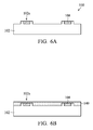
- FIGS. 6A-6D show cross-sectional representations of various stages of forming a cap structure 100 ′′, in accordance with some embodiments of the disclosure.
- the structure in FIG. 6A is the same as the structure in FIG. 1I .
- First bonding layer 108 is embedded in cap substrate 102 .
- a third photoresist layer 140 is formed on first bonding layer 108 and cap substrate 102 as shown in FIG. 6B in accordance with some embodiments of the disclosure.
- third photoresist layer 140 is patterned by a patterning process to form a patterned third photoresist layer 140 as shown in FIG. 6C in accordance with some embodiments of the disclosure.
- Patterned third photoresist layer 140 is used to protect underlying first bonding layer 108 and a portion of cap substrate 102 from being etched.
- the top surface and the sidewalls of extending portion 102 a are covered by patterned third photoresist layer 140 .
- extending portion 102 a has a stair-like shape.
- a number of cap stopper 112 is formed and surrounded by extending portion 102 a.
- stair-like shaped extending portion 102 a has a first stair having a height H 3 and a second stair having a height H 1 .
- a ratio (H 3 /H 1 ) of the height H 3 to the height H 1 is in a range from about 0.002 to about 100.
- FIG. 7 shows a cross-sectional representation of a semiconductor device structure, in accordance with some embodiments of the disclosure.
- Substrate structure 400 is bonded to cap structure 100 ′′ obtained from FIG. 6D by bonding first bonding layer 108 and second bonding layer 204 .
- cap substrate 102 is bonded to MEMS substrate 202 by bonding first bonding layer 108 and second bonding layer 204 .
- the bonding is performed through an eutectic bonding process.
- FIGS. 8A-8B show cross-sectional representations of a semiconductor device structure 20 , in accordance with some embodiments of the disclosure.
- semiconductor substrate 302 has a top surface 302 a and a bottom surface 302 b .
- MEMS substrate 202 is formed on top surface 302 a of semiconductor substrate 302 .
- a cap structure 100 a is bonded to substrate structure 400 by bonding second bonding layer 204 to semiconductor substrate 302 .
- Movable element 202 m is surrounded by extending portion 102 a of cap substrate 102 of cap structure 100 a.
- a cap structure 100 b is bonded to substrate structure 400 by bonding second bonding layer 204 to semiconductor substrate 302 .
- Extending portion 102 a of cap substrate 102 of cap structure 100 b has a stair-like shape.
- first bonding layer 108 is embedded in cap substrate 102 . Therefore, during the eutectic bonding process, the melted alloy with the liquid phase is not squeezed by the bonding force. In addition, extending portion 102 a of cap substrate 102 provides a protection to first bonding layer 108 , and therefore first bonding layer 108 is prevented from being oxidized and hydrolyzed.
- a cap structure includes a cap substrate and a first bonding layer embedded in cap substrate.
- a substrate structure includes a MEMS substrate and a semiconductor substrate, and a second bonding layer is formed on the MEMS substrate.
- the cap structure is bonded to the semiconductor substrate or the MEMS substrate by bonding first bonding layer and the second bonding layer by an eutectic bonding process to form the semiconductor device structure. Because the first bonding layer is embedded in the cap substrate, a portion of first bonding layer and/or second bonding layer is not squeezed by the eutectic bonding process. Therefore, the squeezing problem is avoided.
- first bonding layer is not easily oxidized and hydrolyzed when it is protected by the surrounding cap substrate. As a result, an oxidation and hydrolysis problems are also resolved. Furthermore, the quality and reliability of semiconductor device structure are improved.
- a semiconductor device structure includes a cap structure.
- the cap structure includes: a first bonding layer and a cap substrate, and the first bonding layer is embedded in the cap substrate.
- the semiconductor device structure also includes a substrate structure.
- the substrate structure includes a substrate and a second bonding layer formed on the substrate.
- the substrate includes a micro-electro-mechanical system (MEMS) substrate or a semiconductor substrate.
- MEMS micro-electro-mechanical system
- a semiconductor device structure in some embodiments, includes a semiconductor substrate having a top surface and a bottom surface.
- the semiconductor device structure also includes a micro-electro-mechanical system (MEMS) substrate formed on the top surface of the semiconductor substrate.
- MEMS substrate has a first surface and a second surface and the second surface is in contact with the top surface of the semiconductor substrate.
- the semiconductor device structure further includes a cap substrate formed on the top surface of the semiconductor substrate or the first surface of the MEMS substrate.
- the cap substrate has an embedded bonding layer, and the cap substrate is bonded to the semiconductor substrate or the MEMS structure by the embedded bonding layer.
- a method for forming a semiconductor device structure includes providing a cap substrate and forming a bonding layer in the cap substrate. The method also includes forming a first photoresist layer on the cap substrate to cover the bonding layer and a portion of the cap substrate. The method further includes etching the cap substrate by using the first photoresist layer as a mask to form an extending portion. The bonding layer is embedded in the extending portion.
Landscapes
- Engineering & Computer Science (AREA)
- Microelectronics & Electronic Packaging (AREA)
- Manufacturing & Machinery (AREA)
- Computer Hardware Design (AREA)
- Micromachines (AREA)
- Physics & Mathematics (AREA)
- Geometry (AREA)
Abstract
Embodiments of a semiconductor device structure are provided. The semiconductor device structure includes a cap structure. The cap structure includes: a first bonding layer and a cap substrate, and the first bonding layer is embedded in the cap substrate. The semiconductor device structure also includes a substrate structure. The substrate structure includes a substrate and a second bonding layer formed on the substrate. The substrate includes a micro-electro-mechanical system (MEMS) substrate or a semiconductor substrate. The cap structure is bonded to the substrate structure by bonding the first bonding layer and the second bonding layer.
Description
Semiconductor devices are used in a variety of electronic applications, such as personal computers, cell phones, digital cameras, and other electronic equipment. Semiconductor devices are typically fabricated by sequentially depositing insulating or dielectric layers, conductive layers, and semiconductive layers of material over a semiconductor substrate, and patterning the various material layers using lithography to form circuit components and elements thereon. Many integrated circuits are typically manufactured on a single semiconductor wafer, and individual dies on the wafer are singulated by sawing between the integrated circuits along a scribe line. The individual dies are typically packaged separately, in multi-chip modules, or in other types of packaging, for example.
Micro-electro mechanical system (MEMS) devices have recently been developed. MEMS devices include devices fabricated using semiconductor technology to form mechanical and electrical features. Examples of the MEMS devices include gears, levers, valves, and hinges. The MEMS devices are implemented in accelerometers, pressure sensors, microphones, actuators, mirrors, heaters, and/or printer nozzles.
Although existing devices and methods for forming the MEMS devices have been generally adequate for their intended purposes, they have not been entirely satisfactory in all respects.
For a more complete understanding of the illustrative embodiments and the advantages thereof, reference is now made to the following descriptions taken in conjunction with the accompanying drawings.
The making and using of various embodiments of the disclosure are discussed in detail below. It should be appreciated, however, that the various embodiments can be embodied in a wide variety of specific contexts. The specific embodiments discussed are merely illustrative, and do not limit the scope of the disclosure.
It is to be understood that the following disclosure provides many different embodiments, or examples, for implementing different features of the disclosure. Specific examples of components and arrangements are described below to simplify the present disclosure. These are, of course, merely examples and are not intended to be limiting. Moreover, the performance of a first process before a second process in the description that follows may include embodiments in which the second process is performed immediately after the first process, and may also include embodiments in which additional processes may be performed between the first and second processes. Various features may be arbitrarily drawn in different scales for the sake of simplicity and clarity. Furthermore, the formation of a first feature over or on a second feature in the description may include embodiments in which the first and second features are formed in direct or indirect contact.
Some variations of the embodiments are described. Throughout the various views and illustrative embodiments, like reference numbers are used to designate like elements. It is understood that additional operations can be provided before, during, and after the method, and some of the operations described can be replaced or eliminated for other embodiments of the method.
Referring to FIG. 1A , a cap substrate 102 is provided. In some embodiments, cap substrate 102 is made of silicon or other elementary semiconductor. In some embodiments, cap substrate 102 is made of silicon carbide, gallium arsenic, indium arsenide, indium phosphide, or other applicable materials.
Afterwards, a first photoresist (PR) layer 120 is formed on cap substrate 102. In some embodiments, first PR layer 120 is a positive resist (positive tone resist). The positive resist is characterized by the exposed regions becoming more soluble in a developer solution.
After first photoresist layer 120 is formed, first photoresist layer 120 is patterned by a patterning process to form a patterned first photoresist layer 120 as shown in FIG. 1B in accordance with some embodiments of the disclosure. The patterning process includes a photolithography process and an etching process. The photolithography processes include photoresist coating (e.g., spin-on coating), soft baking, mask aligning, exposure, post-exposure baking, developing the photoresist, rinsing, drying (e.g., hard baking). The etching process includes a dry etching process or a wet etching process.
After patterned first photoresist layer 120 is formed, a portion of cap substrate 102 is removed by using patterned first photoresist layer 120 as a mask as shown in FIG. 1C in accordance with some embodiments of the disclosure. As a result, trenches 104 are formed in cap substrate 102. In some embodiments, cap substrate 102 is removed by a dry etching process or a wet etching process.
After a portion of cap substrate 102 is removed, patterned first photoresist layer 120 is removed as shown in FIG. 1D in accordance with some embodiments of the disclosure. In some embodiments, patterned first photoresist layer 120 is removed by a dry etching process or a wet etching process.
After patterned first photoresist layer 120 is removed, bonding material 106 is filled into trenches 104 and on cap substrate 102 as shown in FIG. 1E in accordance with some embodiments of the disclosure. In some embodiments, bonding material 106 is made of eutectic material, such as germanium (Ge), aluminum (Al), copper (Cu), titanium (Ti), nickel (Ni), silver (Ag), gold (Au), indium (In), tin (Sn) or silicon (Si).
After bonding material 106 is formed, a planarization process is performed to remove the excess of bonding material 106 as shown in FIG. 1F in accordance with some embodiments of the disclosure. As a result, first bonding layer 108 is formed. In some embodiments, a top surface of first bonding layer 108 is substantially level with a top surface of cap substrate 102. In some embodiments, planarization process is a chemical polishing (CMP) process.
After the planarization process is performed, a second photoresist layer 130 is formed on first bonding layer 108 and cap substrate 102 as shown in FIG. 1G in accordance with some embodiments of the disclosure.
After second photoresist layer 130 is formed, second photoresist layer 130 is patterned by a patterning process to form a patterned second photoresist layer 130 as shown in FIG. 1H in accordance with some embodiments of the disclosure. Patterned second photoresist layer 130 is used to protect underlying first bonding layer 108 from being etched. In some embodiments, patterned second photoresist layer 130 covers first bonding layer 108 and a portion of cap substrate 102.
After patterned second photoresist layer 130 is formed, an etching process is performed to remove unmasked regions as shown in FIG. 1I in accordance with some embodiments of the disclosure. As a result, first bonding layer 108 is formed in an extending portion 102 a of cap substrate 102. Afterwards, patterned second photoresist layer 130 is removed and cap structure 100 is formed.
It should be noted that first bonding layer 108 is embedded in cap substrate 102. In some embodiments, first bonding layer 108 is made of germanium (Ge), and cap substrate 102 is made of silicon (Si). Therefore, germanium (Ge) is surrounded by silicon (Si).
It should be noted that a length L2 of patterned second photoresist layer 130 is larger than a length L1 of first bonding layer 108. Therefore, a portion of cap substrate 102 underlying patterned photoresist layer 130 is not removed. As a result, an embedded first boning layer 108 is formed. In some embodiments, patterned second photoresist layer 130 has the length L2 in a range from about 2 μm to about 2000 μm. In some embodiments, first bonding layer 108 has the length L1 in a range from about 1 μm to about 1000 μm. In some embodiments, a ratio (L2/L1) of the length L2 to the length L1 is in a range from about 1 to about 5.
In some embodiments, a ratio (L1/H1) of the length L1 to the height H1 is in a range from about 0.0025 to about 10000. In some embodiments, a ratio (W1/L1) of the distance W1 to the length L1 is in a range from about 0.0001 to about 200.
As shown in FIG. 3A , MEMS substrate 202 includes a movable element 202 m and fixed element 202 f. Movable element 202 m is also called as a proof mass. Movable element 202 m is supported by middle third bonding layer 306 c. In some embodiments, movable element 202 m is made of silicon-containing material, such as polysilicon, amorphous silicon, or crystalline silicon.
In some embodiments, third bonding layer 306 is made of dielectric layer, such as silicon oxide, silicon nitride, silicon oxynitride, spin-on glass (SOG), low-k material, fluoride-doped silicate glass (FSG), carbon doped silicon oxide or other applicable materials. In some embodiments, third bonding layer 306 includes multiple dielectric layers of dielectric materials.
As shown in FIG. 3A , substrate structure 400 is bonded to cap structure 100 by bonding first bonding layer 108 and second bonding layer 204. More specifically, cap substrate 102 is bonded to MEMS substrate 202 by bonding first bonding layer 108 and second bonding layer 204. In some embodiments, the bonding is performed through an eutectic bonding process. The eutectic bonding process is performed with a bonding force at a certain temperature. As a result, an eutectic alloy is formed from first bonding layer 108 and second bonding layer 204.
During the eutectic bonding process, melted alloy has a liquid phase which is easily spilled out. Therefore, a portion of first bonding layer 108 and/or second bonding layer 204 may be squeezed by the bonding force. In addition, first bonding layer (such as Ge) 108 is easily oxidized and hydrolyzed when it is exposed. The squeezing, oxidation and hydrolysis problems may affect the quality and reliability of semiconductor device structure 10.
In order to solve the above problems, first bonding layer 108 is surrounded by cap substrate 102. In other words, there is a distance W1 between the edge of first bonding layer 108 and the edge of extending portion 102 a. More specifically, the edge of first bonding layer 108 is not aligned with the edge of extending portion 102 a. When the eutectic bonding process is performed, the melted alloy with the liquid phase between first bonding layer 108 and second bonding layer 204 is blocked by cap substrate 102. Therefore, squeezing problem is avoided. In other words, cap substrate 102 prevents the melted alloy from spilling out. In addition, due to the protection of cap substrate 102 and extending portion 102 a, first bonding layer 108 is prevented from being oxidized and hydrolyzed.
In some embodiment, the eutectic bonding process is performed at a temperature depending on an eutectic temperature of first bonding layer 108 and second bonding layer 204. In some embodiments, the bonding temperature is higher than the eutectic temperature in a range from about 1 fold to about 1.1 folds. In some embodiments, when first bonding layer 108 is made of germanium (Ge), second bonding layer 204 is made of aluminum (Al), the eutectic bonding process is performed at a temperature in a range from about 420° C. to about 460° C. In some embodiment, the eutectic bonding process is performed at a pressure in a range from about 30 kN to about 300 kN. The eutectic bonding process may be performed in a controlled atmosphere (e.g., in the presence of a forming gas). Example forming gases include Ar, N2, H2, He, N2/H2, or combinations thereof. An alignment process is performed prior to the eutectic bonding process.
In some embodiments, a surface cleaning process is performed prior to the eutectic bonding process. The surface clean process may include a wet etching process, a dry etching process, or combinations thereof. For example, the wet etching process includes exposure to hydrofluoric acid (HF). The dry etching process includes argon sputtering and plasma etching process. In some embodiments, a post-bonding thermal process is performed.
As shown in FIG. 3B , movable element 202 m is supported by a middle third bonding layer 306 c. Two metal layers 304 are formed adjacent to middle third bonding layer 306 c and on semiconductor substrate 302. Two metal layers 304 below middle third bonding layer 306 c are used as stoppers. The stoppers are configured to prevent movable element 202 m from moving too far in the Z-direction and contacting other components or parts during a shock event.
As shown in FIG. 3C , an oxide layer 310 is formed on metal layer 304. Oxide layer 310 is used as the stopper. A capacitor structure is constructed by metal layer 304, oxide layer 310 and movable element 202 m. On the left side of middle third bonding layer 306 c, a first capacitor structure is formed. On the right side of middle third bonding layer 306 c, a second capacitor structure is formed. An acceleration difference between the left side and right side of movable element 202 m is obtained by determining the capacitance differences between the first capacitor structure and the second capacitor structure.
As shown in FIG. 3D , one oxide layer 310 is disposed between two metal layers 304. Therefore, capacitor structure is constructed by two metal layers 304 and one oxide layer 310. Similar to FIG. 3C , on the left side of middle third bonding layer 306 c, a first capacitor structure is formed. On the right side of middle third bonding layer 306 c, a second capacitor structure is formed. Therefore, an acceleration difference between the left side and right side of movable element 202 m is obtained by determining the capacitance differences between the first capacitor structure and the second capacitor structure. In FIG. 3C , oxide layer 310 is formed on metal layer 304, but in FIG. 3D , oxide layer 310 is formed between two metal layers 304.
As shown in FIG. 3E , on the left side of middle third bonding layer 306 c, oxide layer 310 is formed adjacent to metal layer 304. On the right side of middle third bonding layer 306 c, another oxide layer 310 is formed adjacent to another metal layer 304. A capacitor structure is constructed by two metal layers 304 and movable element 202 m. Oxide layer 310 in FIG. 3E is also used as the stopper.
Afterwards, a third photoresist layer 140 is formed on first bonding layer 108 and cap substrate 102 as shown in FIG. 4B in accordance with some embodiments of the disclosure.
After third photoresist layer 140 is formed, third photoresist layer 140 is patterned by a patterning process to form a patterned first photoresist layer 140 as shown in FIG. 4C in accordance with some embodiments of the disclosure. Patterned third photoresist layer 140 is used to protect underlying first bonding layer 108 and a portion of cap substrate 102 from being etched. In some embodiments, patterned third photoresist layer 140 covers a top surface of extending portion 102 a without coving the sidewalls of extending portion 102 a.
After patterned third photoresist layer 140 is formed, an etching process is performed to remove unmasked regions as shown in FIG. 4D in accordance with some embodiments of the disclosure. As a result, the height of extending portion 102 a is elongated from H1 to H2. In some embodiments, the height (H2) of extending portion 102 a is greater than the height (H1) of first bonding layer 108.
A portion of cap substrate 102 is removed to form a number of cap stopper 112 surrounded by extending portion 102 a. Cap stopper 112 is configured to prevent movable element 202 m from moving too far in the Z-direction and contacting other components or parts during a shock event. Afterwards, patterned third photoresist layer 140 is removed and cap structure 100′ is formed.
Afterwards, a third photoresist layer 140 is formed on first bonding layer 108 and cap substrate 102 as shown in FIG. 6B in accordance with some embodiments of the disclosure.
After third photoresist layer 140 is formed, third photoresist layer 140 is patterned by a patterning process to form a patterned third photoresist layer 140 as shown in FIG. 6C in accordance with some embodiments of the disclosure. Patterned third photoresist layer 140 is used to protect underlying first bonding layer 108 and a portion of cap substrate 102 from being etched. In some embodiments, the top surface and the sidewalls of extending portion 102 a are covered by patterned third photoresist layer 140.
After patterned third photoresist layer 140 is formed, an etching process is performed to remove unmasked regions as shown in FIG. 6D in accordance with some embodiments of the disclosure. As a result, extending portion 102 a has a stair-like shape. In addition, a number of cap stopper 112 is formed and surrounded by extending portion 102 a.
As shown in FIG. 6D , stair-like shaped extending portion 102 a has a first stair having a height H3 and a second stair having a height H1. In some embodiments, a ratio (H3/H1) of the height H3 to the height H1 is in a range from about 0.002 to about 100.
As shown in FIG. 8A , semiconductor substrate 302 has a top surface 302 a and a bottom surface 302 b. MEMS substrate 202 is formed on top surface 302 a of semiconductor substrate 302. A cap structure 100 a is bonded to substrate structure 400 by bonding second bonding layer 204 to semiconductor substrate 302. Movable element 202 m is surrounded by extending portion 102 a of cap substrate 102 of cap structure 100 a.
As shown in FIG. 8B , a cap structure 100 b is bonded to substrate structure 400 by bonding second bonding layer 204 to semiconductor substrate 302. Extending portion 102 a of cap substrate 102 of cap structure 100 b has a stair-like shape.
It should be noted that first bonding layer 108 is embedded in cap substrate 102. Therefore, during the eutectic bonding process, the melted alloy with the liquid phase is not squeezed by the bonding force. In addition, extending portion 102 a of cap substrate 102 provides a protection to first bonding layer 108, and therefore first bonding layer 108 is prevented from being oxidized and hydrolyzed.
Embodiments of a semiconductor device structure are provided. A cap structure includes a cap substrate and a first bonding layer embedded in cap substrate. A substrate structure includes a MEMS substrate and a semiconductor substrate, and a second bonding layer is formed on the MEMS substrate. The cap structure is bonded to the semiconductor substrate or the MEMS substrate by bonding first bonding layer and the second bonding layer by an eutectic bonding process to form the semiconductor device structure. Because the first bonding layer is embedded in the cap substrate, a portion of first bonding layer and/or second bonding layer is not squeezed by the eutectic bonding process. Therefore, the squeezing problem is avoided. In addition, first bonding layer is not easily oxidized and hydrolyzed when it is protected by the surrounding cap substrate. As a result, an oxidation and hydrolysis problems are also resolved. Furthermore, the quality and reliability of semiconductor device structure are improved.
In some embodiments, a semiconductor device structure is provided. The semiconductor device structure includes a cap structure. The cap structure includes: a first bonding layer and a cap substrate, and the first bonding layer is embedded in the cap substrate. The semiconductor device structure also includes a substrate structure. The substrate structure includes a substrate and a second bonding layer formed on the substrate. The substrate includes a micro-electro-mechanical system (MEMS) substrate or a semiconductor substrate. The cap structure is bonded to the substrate structure by bonding the first bonding layer and the second bonding layer.
In some embodiments, a semiconductor device structure is provided. The semiconductor device structure includes a semiconductor substrate having a top surface and a bottom surface. The semiconductor device structure also includes a micro-electro-mechanical system (MEMS) substrate formed on the top surface of the semiconductor substrate. The MEMS substrate has a first surface and a second surface and the second surface is in contact with the top surface of the semiconductor substrate. The semiconductor device structure further includes a cap substrate formed on the top surface of the semiconductor substrate or the first surface of the MEMS substrate. The cap substrate has an embedded bonding layer, and the cap substrate is bonded to the semiconductor substrate or the MEMS structure by the embedded bonding layer.
In some embodiments, a method for forming a semiconductor device structure is provided. The method includes providing a cap substrate and forming a bonding layer in the cap substrate. The method also includes forming a first photoresist layer on the cap substrate to cover the bonding layer and a portion of the cap substrate. The method further includes etching the cap substrate by using the first photoresist layer as a mask to form an extending portion. The bonding layer is embedded in the extending portion.
Although embodiments of the present disclosure and their advantages have been described in detail, it should be understood that various changes, substitutions and alterations can be made herein without departing from the spirit and scope of the disclosure as defined by the appended claims. For example, it will be readily understood by those skilled in the art that many of the features, functions, processes, and materials described herein may be varied while remaining within the scope of the present disclosure. Moreover, the scope of the present application is not intended to be limited to the particular embodiments of the process, machine, manufacture, composition of matter, means, methods and steps described in the specification. As one of ordinary skill in the art will readily appreciate from the disclosure of the present disclosure, processes, machines, manufacture, compositions of matter, means, methods, or steps, presently existing or later to be developed, that perform substantially the same function or achieve substantially the same result as the corresponding embodiments described herein may be utilized according to the present disclosure. Accordingly, the appended claims are intended to include within their scope such processes, machines, manufacture, compositions of matter, means, methods, or steps. In addition, each claim constitutes a separate embodiment, and the combination of various claims and embodiments are within the scope of the disclosure.
Claims (20)
1. A semiconductor device structure, comprising:
a substrate, wherein the substrate comprises a micro electro mechanical system (MEMS) substrate or a semiconductor substrate;
a cap substrate disposed above the substrate, wherein the cap substrate comprises an extending portion extending from a bottom surface of the cap substrate towards the substrate;
an eutectic alloy formed between the cap structure and the substrate, wherein at least two of the outer sidewalls of the eutectic alloy are in direct contact with the cap substrate; and
a bonding layer formed between the cap structure and the substrate, wherein the bonding layer is in contact with the extending portion and the substrate,
wherein the eutectic alloy is made of a first material and a second material, and the bonding layer is made of one of the first material and the second material.
2. The semiconductor device structure as claimed in claim 1 , wherein the bonding layer comprises germanium (Ge), aluminum (Al), copper (Cu), titanium (Ti), nickel (Ni), silver (Ag), gold (Au), indium (In), tin (Sn), silicon (Si) or combinations thereof.
3. The semiconductor device structure as claimed in claim 1 , wherein the eutectic alloy is in direct contact with the semiconductor substrate or the MEMS substrate.
4. The semiconductor device structure as claimed in claim 1 , wherein the semiconductor substrate further comprises a complementary metal-oxide semiconductor (CMOS) device.
5. The semiconductor device structure as claimed in claim 1 , wherein there is a distance between an edge of the eutectic alloy and an edge of the extending portion of the cap substrate when seen from a cross-sectional view.
6. The semiconductor device structure as claimed in claim 1 , wherein the cap substrate further comprises a cavity surrounded by the extending portion, and the cavity is defined by an inner sidewall of the extending portion.
7. The semiconductor device structure as claimed in claim 1 , wherein the cap substrate further comprises a cap stopper which is surrounded by the extending portion but is spaced apart from the extending portion.
8. The semiconductor device structure as claimed in claim 7 , wherein the cap stopper is formed in the cavity.
9. The semiconductor device structure as claimed in claim 1 , wherein a height of the extending portion is substantially equal to a height of the eutectic alloy.
10. The semiconductor device structure as claimed in claim 1 , wherein the bonding layer is in contact with the eutectic alloy.
11. A semiconductor device structure, comprising:
a semiconductor substrate having a top surface and a bottom surface;
a micro-electro-mechanical system (MEMS) substrate formed on the top surface of the semiconductor substrate, wherein the MEMS substrate has a first surface and a second surface, and the second surface is in contact with the top surface of the semiconductor substrate; and
a cap substrate formed on the top surface of the semiconductor substrate or the first surface of the MEMS substrate, wherein the cap substrate has an extending portion extending from a bottom surface of the cap substrate towards the semiconductor substrate;
an eutectic alloy formed between the cap substrate and the MEMS substrate or between the cap substrate and the semiconductor substrate, wherein at least two of the outer sidewalls of the eutectic alloy are in direct contact with the cap substrate; and
a bonding layer formed between the cap substrate and the MEMS substrate or between the cap substrate and the semiconductor substrate, wherein the bonding layer is in contact with the extending portion and one of the MEMS substrate and the cap substrate,
wherein the eutectic alloy is made of a first material and a second material, and the bonding layer is made of one of the first material and the second material.
12. The semiconductor device structure as claimed in claim 11 , wherein a portion of the eutectic alloy is surrounded by the bonding layer.
13. The semiconductor device structure as claimed in claim 11 , wherein the extending portion has a stair shape.
14. The semiconductor device structure as claimed in claim 11 , wherein the height of the extending portion is greater than the height of the eutectic alloy.
15. The semiconductor device structure as claimed in claim 11 , wherein the eutectic alloy has a ring structure.
16. The semiconductor device structure as claimed in claim 11 , wherein a portion of the eutectic alloy is surrounded by the extending portion.
17. The semiconductor device structure as claimed in claim 11 , wherein an edge of the eutectic alloy is not aligned with an edge of the extending portion when seen from a cross-sectional view.
18. The semiconductor device structure as claimed in claim 11 , wherein the bonding layer is in contact with the eutectic alloy.
19. A semiconductor device structure, comprising:
a semiconductor substrate;
a MEMS substrate formed over the semiconductor substrate;
a cap substrate formed over the MEMS structure, wherein the cap substrate comprises an extending portion extending from a bottom surface of the cap substrate towards the semiconductor substrate;
an eutectic alloy formed between the cap substrate and the MEMS substrate, wherein at least two of the outer sidewalls of the eutectic alloy are in direct contact with the cap substrate; and
a bonding layer formed between the cap substrate and the MEMS substrate, wherein the bonding layer is in contact with the extending portion and the MEMS substrate, the eutectic alloy is made of a first material and a second material, and the bonding layer is made of one of the first material and the second material.
20. The semiconductor device structure as claimed in claim 19 , wherein the bonding layer is in contact with the eutectic alloy.
Priority Applications (2)
| Application Number | Priority Date | Filing Date | Title |
|---|---|---|---|
| US14/166,492 US9540231B2 (en) | 2014-01-28 | 2014-01-28 | MEMS device with a bonding layer embedded in the cap |
| TW103145408A TWI541999B (en) | 2014-01-28 | 2014-12-25 | Semiconductor device and method for forming the same |
Applications Claiming Priority (1)
| Application Number | Priority Date | Filing Date | Title |
|---|---|---|---|
| US14/166,492 US9540231B2 (en) | 2014-01-28 | 2014-01-28 | MEMS device with a bonding layer embedded in the cap |
Publications (2)
| Publication Number | Publication Date |
|---|---|
| US20150210537A1 US20150210537A1 (en) | 2015-07-30 |
| US9540231B2 true US9540231B2 (en) | 2017-01-10 |
Family
ID=53678378
Family Applications (1)
| Application Number | Title | Priority Date | Filing Date |
|---|---|---|---|
| US14/166,492 Active 2034-04-05 US9540231B2 (en) | 2014-01-28 | 2014-01-28 | MEMS device with a bonding layer embedded in the cap |
Country Status (2)
| Country | Link |
|---|---|
| US (1) | US9540231B2 (en) |
| TW (1) | TWI541999B (en) |
Cited By (2)
| Publication number | Priority date | Publication date | Assignee | Title |
|---|---|---|---|---|
| KR20190036490A (en) * | 2017-09-27 | 2019-04-04 | 타이완 세미콘덕터 매뉴팩쳐링 컴퍼니 리미티드 | An integration scheme for wafer level packaging |
| US11279615B2 (en) | 2017-09-27 | 2022-03-22 | Taiwan Semiconductor Manufacturing Company, Ltd. | Method for manufacturing a MEMS device by first hybrid bonding a CMOS wafer to a MEMS wafer |
Families Citing this family (12)
| Publication number | Priority date | Publication date | Assignee | Title |
|---|---|---|---|---|
| CN105084294A (en) * | 2014-04-21 | 2015-11-25 | 中芯国际集成电路制造(上海)有限公司 | MEMS device, preparation method thereof and electronic device |
| CN106373900A (en) * | 2015-07-20 | 2017-02-01 | 中芯国际集成电路制造(北京)有限公司 | Wafer level bonding packaging method and eutectic bonding type wafer structure |
| US20170057810A1 (en) * | 2015-09-01 | 2017-03-02 | Apple Inc. | Strain Reduction and Sensing on Package Substrates |
| FR3041625B1 (en) * | 2015-09-29 | 2021-07-30 | Tronics Microsystems | DEVICE FOR FIXING TWO ELEMENTS SUCH AS A CHIP, AN INTERPOSER AND A BRACKET |
| US10629468B2 (en) | 2016-02-11 | 2020-04-21 | Skyworks Solutions, Inc. | Device packaging using a recyclable carrier substrate |
| US20170243739A1 (en) * | 2016-02-24 | 2017-08-24 | Skyworks Solutions, Inc. | 3d micromold and pattern transfer |
| US10453763B2 (en) | 2016-08-10 | 2019-10-22 | Skyworks Solutions, Inc. | Packaging structures with improved adhesion and strength |
| WO2019159410A1 (en) * | 2018-02-14 | 2019-08-22 | 株式会社村田製作所 | Resonance device and resonance device manufacturing method |
| DE102018219524A1 (en) * | 2018-11-15 | 2020-05-20 | Robert Bosch Gmbh | Process for producing a microelectromechanical sensor and microelectromechanical sensor |
| CN111115555B (en) * | 2019-12-20 | 2023-08-29 | 北京航天控制仪器研究所 | A silicon groove structure and preparation method for MEMS wafer-level eutectic bonding package |
| DE102020215021A1 (en) | 2020-11-30 | 2022-06-02 | Robert Bosch Gesellschaft mit beschränkter Haftung | Micromechanical device with electrically contacted cap |
| CN116514050A (en) * | 2022-11-17 | 2023-08-01 | 上海华虹宏力半导体制造有限公司 | Motion sensor and method of manufacturing the same |
Citations (10)
| Publication number | Priority date | Publication date | Assignee | Title |
|---|---|---|---|---|
| US20040200736A1 (en) * | 2003-04-09 | 2004-10-14 | Van Heerden David Peter | Hermetically sealed product and related methods of manufacture |
| US20060115323A1 (en) * | 2004-11-04 | 2006-06-01 | Coppeta Jonathan R | Compression and cold weld sealing methods and devices |
| US20060197215A1 (en) * | 2005-03-03 | 2006-09-07 | Stellar Microdevices, Inc. | Hermetic MEMS package and method of manufacture |
| US20100258884A1 (en) * | 2009-04-14 | 2010-10-14 | Julian Gonska | Method for attaching a first carrier device to a second carrier device and micromechanical components |
| US20120148870A1 (en) * | 2010-12-09 | 2012-06-14 | Taiwan Semiconductor Manufacturing Company, Ltd. | Self-removal anti-stiction coating for bonding process |
| US20130068022A1 (en) * | 2011-09-15 | 2013-03-21 | Samsung Electro-Mechanics Co., Ltd. | Micro electro mechanical systems component |
| US20130203199A1 (en) * | 2012-02-02 | 2013-08-08 | Taiwan Semiconductor Manufacturing Company, Ltd. | Methods of Bonding Caps for MEMS Devices |
| US20130285175A1 (en) * | 2012-04-25 | 2013-10-31 | Robert Bosch Gmbh | Micromechanical component and method for manufacturing a micromechanical component |
| US20140124899A1 (en) * | 2012-11-02 | 2014-05-08 | Raytheon Company | Integrated bondline spacers for wafer level packaged circuit devices |
| US20140131850A1 (en) * | 2012-11-09 | 2014-05-15 | Analog Devices, Inc. | Microchip with blocking apparatus and method of fabricating microchip |
-
2014
- 2014-01-28 US US14/166,492 patent/US9540231B2/en active Active
- 2014-12-25 TW TW103145408A patent/TWI541999B/en active
Patent Citations (10)
| Publication number | Priority date | Publication date | Assignee | Title |
|---|---|---|---|---|
| US20040200736A1 (en) * | 2003-04-09 | 2004-10-14 | Van Heerden David Peter | Hermetically sealed product and related methods of manufacture |
| US20060115323A1 (en) * | 2004-11-04 | 2006-06-01 | Coppeta Jonathan R | Compression and cold weld sealing methods and devices |
| US20060197215A1 (en) * | 2005-03-03 | 2006-09-07 | Stellar Microdevices, Inc. | Hermetic MEMS package and method of manufacture |
| US20100258884A1 (en) * | 2009-04-14 | 2010-10-14 | Julian Gonska | Method for attaching a first carrier device to a second carrier device and micromechanical components |
| US20120148870A1 (en) * | 2010-12-09 | 2012-06-14 | Taiwan Semiconductor Manufacturing Company, Ltd. | Self-removal anti-stiction coating for bonding process |
| US20130068022A1 (en) * | 2011-09-15 | 2013-03-21 | Samsung Electro-Mechanics Co., Ltd. | Micro electro mechanical systems component |
| US20130203199A1 (en) * | 2012-02-02 | 2013-08-08 | Taiwan Semiconductor Manufacturing Company, Ltd. | Methods of Bonding Caps for MEMS Devices |
| US20130285175A1 (en) * | 2012-04-25 | 2013-10-31 | Robert Bosch Gmbh | Micromechanical component and method for manufacturing a micromechanical component |
| US20140124899A1 (en) * | 2012-11-02 | 2014-05-08 | Raytheon Company | Integrated bondline spacers for wafer level packaged circuit devices |
| US20140131850A1 (en) * | 2012-11-09 | 2014-05-15 | Analog Devices, Inc. | Microchip with blocking apparatus and method of fabricating microchip |
Cited By (4)
| Publication number | Priority date | Publication date | Assignee | Title |
|---|---|---|---|---|
| KR20190036490A (en) * | 2017-09-27 | 2019-04-04 | 타이완 세미콘덕터 매뉴팩쳐링 컴퍼니 리미티드 | An integration scheme for wafer level packaging |
| KR102137103B1 (en) | 2017-09-27 | 2020-07-24 | 타이완 세미콘덕터 매뉴팩쳐링 컴퍼니 리미티드 | An integration scheme for wafer level packaging |
| US11279615B2 (en) | 2017-09-27 | 2022-03-22 | Taiwan Semiconductor Manufacturing Company, Ltd. | Method for manufacturing a MEMS device by first hybrid bonding a CMOS wafer to a MEMS wafer |
| US11932534B2 (en) | 2017-09-27 | 2024-03-19 | Taiwan Semiconductor Manufacturing Company, Ltd. | MEMS device having a metallization structure embedded in a dielectric structure with laterally offset sidewalls of a first portion and a second portion |
Also Published As
| Publication number | Publication date |
|---|---|
| TW201532277A (en) | 2015-08-16 |
| US20150210537A1 (en) | 2015-07-30 |
| TWI541999B (en) | 2016-07-11 |
Similar Documents
| Publication | Publication Date | Title |
|---|---|---|
| US9540231B2 (en) | MEMS device with a bonding layer embedded in the cap | |
| US10508029B2 (en) | MEMS integrated pressure sensor devices and methods of forming same | |
| US10087069B2 (en) | Semiconductor devices with moving members and methods for making the same | |
| US9422153B2 (en) | Support structure for TSV in MEMS structure | |
| US9630832B2 (en) | Semiconductor device and method of manufacturing | |
| US9187317B2 (en) | MEMS integrated pressure sensor and microphone devices and methods of forming same | |
| US8729646B2 (en) | MEMS devices and methods for forming the same | |
| US9139420B2 (en) | MEMS device structure and methods of forming same | |
| TWI543280B (en) | Method for forming MEMS components | |
| KR102137103B1 (en) | An integration scheme for wafer level packaging | |
| US20140264653A1 (en) | MEMS Pressure Sensor and Microphone Devices Having Through-Vias and Methods of Forming Same | |
| US10865100B2 (en) | Method for forming micro-electro-mechanical system (MEMS) structure | |
| CN102891117B (en) | Chip package and manufacturing method thereof | |
| US10351418B2 (en) | Bond rings in semiconductor devices and methods of forming same | |
| TW201727780A (en) | Manufacturing method of MEMS package | |
| CN105023909A (en) | Structure and method of providing a re-distribution layer (RDL) and a through-silicon via (TSV) | |
| US20160145094A1 (en) | Micro-elelctro-mechanical system device and method for fabricating the same | |
| CN103224216A (en) | A microelectronic mechanical system (MEMS) structure equipped with substrate through holes and a forming method therefore | |
| CN104045051A (en) | Stacked semiconductor device and method of forming the same | |
| CN105742193B (en) | Wafer-to-wafer bonding process and structure |
Legal Events
| Date | Code | Title | Description |
|---|---|---|---|
| AS | Assignment |
Owner name: TAIWAN SEMICONDUCTOR MANUFACTURING CO., LTD, TAIWA Free format text: ASSIGNMENT OF ASSIGNORS INTEREST;ASSIGNORS:CHANG, KAI-FUNG;TSAI, LIEN-YAO;LEU, LEN-YI;REEL/FRAME:032076/0888 Effective date: 20140123 |
|
| STCF | Information on status: patent grant |
Free format text: PATENTED CASE |
|
| MAFP | Maintenance fee payment |
Free format text: PAYMENT OF MAINTENANCE FEE, 4TH YEAR, LARGE ENTITY (ORIGINAL EVENT CODE: M1551); ENTITY STATUS OF PATENT OWNER: LARGE ENTITY Year of fee payment: 4 |