US9531349B2 - System and method for controlling radiated EMI using interleaved frequency switching - Google Patents
System and method for controlling radiated EMI using interleaved frequency switching Download PDFInfo
- Publication number
- US9531349B2 US9531349B2 US14/602,939 US201514602939A US9531349B2 US 9531349 B2 US9531349 B2 US 9531349B2 US 201514602939 A US201514602939 A US 201514602939A US 9531349 B2 US9531349 B2 US 9531349B2
- Authority
- US
- United States
- Prior art keywords
- frequency
- steps
- sequence
- span
- system clock
- Prior art date
- Legal status (The legal status is an assumption and is not a legal conclusion. Google has not performed a legal analysis and makes no representation as to the accuracy of the status listed.)
- Active
Links
- 238000000034 method Methods 0.000 title claims description 53
- 230000008859 change Effects 0.000 claims abstract description 12
- 238000004590 computer program Methods 0.000 claims description 8
- 238000004891 communication Methods 0.000 description 14
- 238000005259 measurement Methods 0.000 description 12
- 230000009467 reduction Effects 0.000 description 11
- 238000013459 approach Methods 0.000 description 5
- 238000012545 processing Methods 0.000 description 4
- 230000005540 biological transmission Effects 0.000 description 3
- 230000003287 optical effect Effects 0.000 description 3
- 230000002085 persistent effect Effects 0.000 description 3
- 230000003595 spectral effect Effects 0.000 description 3
- 230000004075 alteration Effects 0.000 description 2
- 239000006227 byproduct Substances 0.000 description 2
- 238000000576 coating method Methods 0.000 description 2
- 230000006870 function Effects 0.000 description 2
- 230000010354 integration Effects 0.000 description 2
- 238000012804 iterative process Methods 0.000 description 2
- 238000012423 maintenance Methods 0.000 description 2
- 238000001228 spectrum Methods 0.000 description 2
- 230000007480 spreading Effects 0.000 description 2
- 238000003491 array Methods 0.000 description 1
- 230000008901 benefit Effects 0.000 description 1
- 239000011248 coating agent Substances 0.000 description 1
- 230000006872 improvement Effects 0.000 description 1
- 239000004973 liquid crystal related substance Substances 0.000 description 1
- 239000000463 material Substances 0.000 description 1
- 229910052751 metal Inorganic materials 0.000 description 1
- 239000002184 metal Substances 0.000 description 1
- 150000002739 metals Chemical class 0.000 description 1
- 238000004806 packaging method and process Methods 0.000 description 1
- 238000012163 sequencing technique Methods 0.000 description 1
- 238000006467 substitution reaction Methods 0.000 description 1
- 229910000859 α-Fe Inorganic materials 0.000 description 1
Images


Classifications
-
- H—ELECTRICITY
- H04—ELECTRIC COMMUNICATION TECHNIQUE
- H04B—TRANSMISSION
- H04B15/00—Suppression or limitation of noise or interference
- H04B15/02—Reducing interference from electric apparatus by means located at or near the interfering apparatus
- H04B15/04—Reducing interference from electric apparatus by means located at or near the interfering apparatus the interference being caused by substantially sinusoidal oscillations, e.g. in a receiver or in a tape-recorder
- H04B15/06—Reducing interference from electric apparatus by means located at or near the interfering apparatus the interference being caused by substantially sinusoidal oscillations, e.g. in a receiver or in a tape-recorder by local oscillators of receivers
-
- H—ELECTRICITY
- H03—ELECTRONIC CIRCUITRY
- H03K—PULSE TECHNIQUE
- H03K3/00—Circuits for generating electric pulses; Monostable, bistable or multistable circuits
- H03K3/01—Details
- H03K3/013—Modifications of generator to prevent operation by noise or interference
-
- H—ELECTRICITY
- H03—ELECTRONIC CIRCUITRY
- H03K—PULSE TECHNIQUE
- H03K19/00—Logic circuits, i.e. having at least two inputs acting on one output; Inverting circuits
- H03K19/003—Modifications for increasing the reliability for protection
- H03K19/00346—Modifications for eliminating interference or parasitic voltages or currents
-
- H—ELECTRICITY
- H03—ELECTRONIC CIRCUITRY
- H03L—AUTOMATIC CONTROL, STARTING, SYNCHRONISATION OR STABILISATION OF GENERATORS OF ELECTRONIC OSCILLATIONS OR PULSES
- H03L7/00—Automatic control of frequency or phase; Synchronisation
Definitions
- This disclosure relates generally to the control of electromagnetic interference (EMI). More specifically, this disclosure relates to a system and method for controlling radiated electromagnetic interference (R-EMI), or simply radiated emissions (RE), using interleaved frequency switching.
- EMI electromagnetic interference
- R-EMI radiated electromagnetic interference
- RE simply radiated emissions
- R-EMI radiated electromagnetic interference
- the RE performance of a system may be evaluated by measuring equipment emissions within a narrow frequency reference window at individual frequencies.
- FCC Federal Communications Commission
- FCC Federal Communications Commission
- CISPR International Special Committee on Radio Interference
- IEC International Electrotechnical Commission
- Measurement involves a time integration of spectral energy of emissions occurring within the reference measurement window. A measured average emission magnitude at each frequency window is compared to published pre-specified limits, and a determination is made as to whether excessive RE is being radiated. If excessive RE is present, steps are taken to bring the RE-emitting system into compliance within acceptable emission limits.
- This disclosure provides a system and method for controlling radiated electromagnetic interference (R-EMI or simply RE) using interleaved frequency switching.
- R-EMI radiated electromagnetic interference
- an apparatus in a first embodiment, includes a controller configured to be coupled to a system clock that generates a clock signal for a device that generates radiated electromagnetic interference (RE).
- the controller is also configured to determine a frequency span associated with the system clock, where the frequency span has a minimum frequency and a maximum frequency.
- the controller is further configured to determine a sequence of frequency steps, where each frequency step is associated with a distinct frequency within the frequency span.
- the controller is configured to control the system clock to change a frequency of the clock signal through the sequence of frequency steps in order to reduce the RE generated at or by the device.
- a method in a second embodiment, includes determining a frequency span associated with a system clock that generates a clock signal for a device that generates RE, where the frequency span has a minimum frequency and a maximum frequency. The method also includes determining a sequence of frequency steps, where each frequency step is associated with a distinct frequency within the frequency span. The method further includes controlling the system clock to change a frequency of the clock signal through the sequence of frequency steps in order to reduce the RE generated at or by the device.
- a non-transitory computer readable medium embodies a computer program.
- the computer program includes computer readable program code for determining a frequency span associated with a system clock that generates a clock signal for a device that generates RE, where the frequency span has a minimum frequency and a maximum frequency.
- the computer program also includes computer readable program code for determining a sequence of frequency steps, where each frequency step is associated with a distinct frequency within the frequency span.
- the computer program further includes computer readable program code for controlling the system clock to change a frequency of the clock signal through the sequence of frequency steps in order to reduce the RE generated at or by the device.
- the frequency steps are interleaved across the frequency span to avoid large frequency jumps.
- a frequency interval between adjacent frequencies in the sequence of frequency steps is determined based on an intermediate frequency (IF) filter bandwidth required by an International Special Committee on Radio Interference (CISPR) standard.
- the frequency interval may be determined such that no two adjacent frequencies in the sequence fall within a single IF filter bandwidth.
- a duration of each frequency step is determined based on the number of frequency steps and the total cycle time.
- the number of frequency steps and the total cycle time are optimally selected based on one or more of: a quasi peak dwell time, a quasi peak decay time, and a time for a phased lock loop to lock.
- FIG. 1 illustrates an example system for controlling radiated electromagnetic interference (R-EMI or RE) by controlling a system clock according to this disclosure
- FIG. 2 illustrates an example method for controlling RE using interleaved frequency switching in accordance with this disclosure
- FIG. 3 illustrates an example interleaved sequence of frequency steps generated using an interleaved frequency switching technique according to this disclosure
- FIGS. 4A and 4B illustrate example results of an interleaved frequency switching method that significantly reduces RE according to this disclosure
- FIG. 5 illustrates front and perspective views of an example electronics housing for electronics that use an interleaved frequency switching method according to this disclosure
- FIG. 6 illustrates an example display configured for operation using an interleaved frequency switching technique according to this disclosure.
- FIG. 7 illustrates an example device for controlling a system clock for interleaved frequency switching according to this disclosure.
- FIGS. 1 through 7 discussed below, and the various embodiments used to describe the principles of the present invention in this patent document are by way of illustration only and should not be construed in any way to limit the scope of the invention. Those skilled in the art will understand that the principles of the invention may be implemented in any type of suitably arranged device or system.
- R-EMI radiated electromagnetic interference
- RE is generated as a byproduct of a clock signal associated with a display signal.
- a clocking frequency of the clock signal typically needs to meet strict timing constraints for an acceptable display performance.
- Some spread spectrum (SS) techniques have been used to reduce RE, but such techniques are of limited benefit due to the following reasons.
- RE measurements are typically performed to assess the “annoyance factor” of RE noise.
- the RE measurements include measuring quasi peaks with an intermediate frequency (IF) filter bandwidth (BW) around 100 kHz to 150 kHz.
- IF intermediate frequency
- BW filter bandwidth
- the frequency is spread to approximately a few hundred parts per million (ppm) of the center frequency, which is typically at tens of mega-Hertz.
- ppm parts per million
- the quasi peak measurement shows little or no improvement compared to a normal clocking scenario since power remains concentrated in one or two bands only instead of spreading out.
- the peaks associated with SS might actually go higher than clocking without SS.
- the quasi peak value depends on the peak amplitude, repetition rate, and duration of the peak.
- Quasi peak detectors have an attack time on the order of milliseconds (such as 1 ms for CISPR 11) and a decay time on the order of a few hundred milliseconds (such as 500 ms for CISPR 11).
- the repetition rate and duration of the clock should be chosen properly. If the frequency is switched too fast (which is the case in many SS techniques) or too slow, it is highly likely that the quasi peak will not show any reduction in the measured value.
- PLL phase locked loop
- some methods seek to limit RE using, for example, conductive coatings, ferrite clamps, or shielded wires. Such methods require extra hardware or materials, thus increasing costs and limiting feasibility.
- Other methods seek to reduce RE using, for example, slew rate reduction, phase modulation, impedance matching, or frequency hopping. However, such methods typically result in significant complexity and may offer minimal RE reduction. Also, depending on the complexity, such methods may not always be feasible to implement in an available piece of hardware.
- embodiments of this disclosure control RE by manipulating a system clock.
- these approaches can be implemented in software or firmware in existing microcontroller- or microprocessor-based systems without any extra hardware. These approaches thus reduce or eliminate dependency on external components, thereby reducing costs and resulting in a simpler designs.
- the approaches disclosed here are generally applicable to any suitable microcontroller- or microprocessor-based clocked data transmission systems. For ease of explanation, certain embodiments are described specifically in connection with systems driving an LCD (which is one of the most commonly available display types), although the approaches described here could be used in any other suitable system.
- FIG. 1 illustrates an example system 100 for controlling RE by controlling a system clock according to this disclosure.
- the system 100 includes a clock controller 102 , a system clock 104 , and a controlled device 106 .
- the controlled device 106 represents a device that transmits or receives data and that operates under the control of the system clock 104 .
- the controlled device 106 represents an LCD display.
- One aspect of the controlled device 106 is that it generates RE 108 as a result of its operation.
- an LCD or one or more components associated with the LCD
- RE can significantly affect image quality or cause problems with nearby electronics.
- the system clock 104 generates a clock signal associated with operation of the controlled device 106 .
- the clock signal may be used to time a command signal that is transmitted to the controlled device 106 .
- a frequency of the clock signal generated by the system clock 104 can be adjusted according to instructions received from the clock controller 102 .
- the clock controller 102 controls the system clock 104 to rapidly change its clock frequency.
- the clock controller 102 controls the system clock 104 by transmitting command signals or instructions to the system clock 104 in order to change the clock frequency.
- Sufficiently rapid frequency changes reduce the amount of time that frequency components fall within the narrow RE-compliance reference bandwidth. Since RE measurements represent an integration of spectral energy over time, reducing the time that spectral components fall within the reference bandwidth reduces their RE contribution.
- the clock controller 102 controls the system clock 104 to change the frequency of its clock signal using an interleaved frequency switching technique. Interleaving of the frequency steps as described below avoids large jumps in frequency even for large spreads. This results in good operational performance for an LCD or other device, even for a large overall frequency spread.
- the clock controller 102 controls the duration, repetition rate, and spread of the steps by optimizing on multiple parameters, resulting in significant RE reduction.
- the clock controller 102 performs a method to determine a set of interleaved frequencies for switching the system clock 104 in order to reduce RE generated by the controlled device 106 . Such a method is described with respect to FIG. 2 below.
- FIG. 1 illustrates one example of a system 100 for controlling RE using an interleaved frequency switching technique
- various changes may be made to FIG. 1 .
- various components in FIG. 1 could be combined, further subdivided, or omitted and additional components could be added according to particular needs.
- various components of the clock controller 102 , the system clock 104 , and the controlled device 106 could be arranged together in one housing or on one circuit board.
- FIG. 2 illustrates an example method 200 for controlling RE using interleaved frequency switching in accordance with this disclosure.
- the method 200 is described as being performed by the clock controller 102 in association with the system 100 of FIG. 1 .
- the method 200 could be used with any other suitable device and in any other suitable system.
- the clock controller 102 identifies a center frequency f C of the system clock 104 that allows for a maximum span f SPAN .
- the center frequency f C may be provided by a user or engineer at runtime or during a maintenance window; read from a file, table, or other data structure; or otherwise obtained in any suitable manner.
- the allowed span f SPAN may be determined based on the capability of the controlled device 106 , such as described in its datasheet.
- the allowed maximum span f SPAN may be determined by one or more timing parameters associated with the LCD, such as the span for which those parameters do not change outside the allowed limit.
- the clock controller 102 validates that the performance of the system 100 meets the requirements with specified frequency extremes f MAX and f MIN without any hardware change. Minor changes in firmware that can be performed at runtime are acceptable.
- the clock controller 102 based on electromagnetic compliance (EMC) certification requirements, the clock controller 102 identifies various parameters related to an RE measurement, such as:
- the clock controller 102 selects a frequency hop step size f STEP .
- the frequency hop step size f STEP can be selected for optimum power distribution. In general, a larger step results in a better power distribution. However, because the overall spread is fixed, the number of steps is reduced as the step size is increased.
- the value of t STEP may ideally be as small as possible, which can help to ensure a minimum footprint for each frequency step.
- the value of t STEP could be at least five times the time t LOCK it takes for a PLL to lock (which is typically on the order of a few hundreds of microseconds).
- t STEP could give ample time for the QPD value to decay during an off period (such as the time when other frequencies are being stepped).
- a value of at least four times t DECAY is a good choice. Because this may be an important constraint to adhere to, t STEP can be increased if required.
- t STEP In determining the value of t STEP , the following constraint may also be met if possible: t CYCLE ⁇ t STEP >4 ⁇ t DECAY (8) In some embodiments, this constraint should be met, but it could be relaxed somewhat when other constraints are difficult to meet.
- the values N STEPS and t STEP can be calculated interdependently (such as by using an iterative process) until suitable values for t STEP and t CYCLE are determined.
- the clock controller 102 sequences the frequency steps so that they are interleaved. This could occur as indicated below. For embodiments where the value of N STEPS is odd:
- the clock controller 102 implements this sequencing. This can be accomplished by controlling the clock frequency of the system clock 104 according to the sequence, with the duration of each step as t STEP .
- the method 200 could be implemented in any suitable manner, such as by using hardware or a combination of software/firmware and hardware.
- the method 200 can be enabled in firmware using an interrupt service routine (ISR), where a frequency register or control can be updated.
- ISR interrupt service routine
- the RE can be measured after this method 200 to validate the reduction in quasi peaks. However, it should be noted that actual RE reduction may be lower than expected due to peaking that occurs because of switching. If conditions require further RE reduction, the annoyance factor could be reduced by improving any one or more of the above-mentioned conditions.
- the following example implementation of the method 200 is provided.
- the following parameters can be determined based on CISPR 11 requirements:
- the frequencies are selected such that no two adjacent frequencies fall within a single IF bandwidth. This can help to ensure an optimum power distribution to reduce RE significantly. Also, the frequencies are interleaved and steadily rise and fall along the sequence such that adjacent frequencies do not represent a significant jump. This includes going from the last frequency in a sequence (62.9 MHz) to the first frequency in the next sequence (62.7 MHz). Thus, large jumps in frequency are avoided, even for large overall spreads of frequency.
- FIG. 2 illustrates one example of a method 200 for controlling RE using interleaved frequency switching
- various changes may be made to FIG. 2 .
- steps shown in FIG. 2 could overlap, occur in parallel, occur in a different order, or occur multiple times.
- some steps could be combined or removed and additional steps could be added according to particular needs.
- FIG. 3 illustrates one example of an interleaved sequence of frequency steps 300 generated using an interleaved frequency switching technique, various changes may be made to FIG. 3 .
- the method 200 has been described as identifying a sequence of frequencies that rise from a minimum frequency to a maximum frequency and then descend to the minimum frequency again, other arrangements of frequencies in the sequence are possible.
- the sequence of frequencies could start at the maximum frequency, descend to the minimum frequency, and then rise to approximately the maximum frequency at the end of the sequence. That is, instead of a “mountain” sequence (low-high-low), the sequence of frequencies could be a “valley” sequence (high-low-high).
- Other frequency sequences may also be suitable, such as low-high-low-high-low.
- each frequency step can be selected to be adequately large for a PLL to lock and settle, thereby lowering a repetition rate. However, the time duration is also kept small enough to provide an optimum ON duration. This ensures lower quasi peak values. Also, there are enough frequency steps to help ensure that (1) the repetition rate is low enough for a good RE reduction while (2) the overall spread is limited to be within the timing constraint window of the RE-producing controlled device 106 (such as an LCD display).
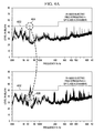
- FIGS. 4A and 4B illustrate example results of an interleaved frequency switching method that significantly reduces RE according to this disclosure.
- the method 200 can result in a significant reduction in RE.
- a stepped horizontal line 402 represents a quasi peak limit for RE according to the CISPR 11 standard.
- a quasi peak measurement in a system with no interleaved frequency switching is very near the acceptable limit for that frequency.
- the system when modified to use interleaved frequency switching (such as in the system 100 ), results in quasi peak measurements several dB below the limit as indicated at region 406 in FIG. 4A .
- FIG. 4B provides numerical results associated with the two approaches.
- the reduction in RE using the method 200 can allow for reduced electronics packaging or housing costs.
- FIG. 5 illustrates front and perspective views of an electronics housing 500 for electronics that use the method 200 according to this disclosure. Because RE is reduced, the electronics in the housing 500 do not require certain kinds of conductive coating and can be spaced closer together. This allows for a slimmer, lower-profile housing 500 . Also, the housing 500 can be formed of plastic, instead of one or more RE-shielding metals, thereby reducing overall cost and weight.
- FIG. 6 illustrates an example display 600 configured for operation using an interleaved frequency switching technique according to this disclosure.
- the display 600 could, for example, represent the controlled device 106 in the system 100 of FIG. 1 .
- the display 600 includes a graphic chipset 602 , an LCD transmitter 604 , and an LCD 606 .
- the display 600 receives one or more data signals and clock signals and uses the signals at the graphic chipset 602 and the LCD transmitter 604 in order to generate images at the LCD 606 .
- the display 600 can receive one or more clock signals from a system clock, such as the system clock 104 .
- the LCD 606 and the LCD transmitter 604 may be connected together through one or more connectors or cable harnesses as known in the art.
- the display 600 generates RE 608 during its operation.
- the display 600 can generate the RE 608 while displaying an image at the LCD 606 .
- the RE 608 can be mitigated by performing interleaved frequency switching on one or more clock signals associated with generating the display at the LCD 606 .
- FIG. 6 illustrates one example of a display 600 configured for operation using an interleaved frequency switching technique
- various changes may be made to FIG. 6 .
- various components in FIG. 6 could be combined, further subdivided, or omitted and additional components could be added according to particular needs.
- FIG. 7 illustrates an example device 700 for controlling a system clock for interleaved frequency switching according to this disclosure.
- the device 700 could, for example, represent a computing device that implements the system 100 of FIG. 1 .
- the device 700 could represent any other suitable device for controlling a system clock.
- the device 700 can include a bus system 702 , which supports communication between at least one processing device 704 , at least one storage device 706 , at least one communications unit 708 , and at least one input/output (I/O) unit 710 .
- the processing device 704 executes instructions that may be loaded into a memory 712 .
- the processing device 704 may include any suitable number(s) and type(s) of processors or other devices in any suitable arrangement.
- Example types of processing devices 704 include microprocessors, microcontrollers, digital signal processors, field programmable gate arrays, application specific integrated circuits, and discrete circuitry.
- the memory 712 and a persistent storage 714 are examples of storage devices 706 , which represent any structure(s) capable of storing and facilitating retrieval of information (such as data, program code, and/or other suitable information on a temporary or permanent basis).
- the memory 712 may represent a random access memory or any other suitable volatile or non-volatile storage device(s).
- the persistent storage 714 may contain one or more components or devices supporting longer-term storage of data, such as a ready only memory, hard drive, Flash memory, or optical disc.
- the memory 712 and the persistent storage 714 may be configured to store instructions associated with controlling a system clock for interleaved frequency switching.
- the communications unit 708 supports communications with other systems or devices, such as the system clock 104 .
- the communications unit 708 could include a network interface card that facilitates communications over at least one Ethernet network.
- the communications unit 708 could also include a wireless transceiver facilitating communications over at least one wireless network.
- the communications unit 708 may support communications through any suitable physical or wireless communication link(s).
- the I/O unit 710 allows for input and output of data.
- the I/O unit 710 may provide a connection for user input through a keyboard, mouse, keypad, touchscreen, or other suitable input device.
- the I/O unit 710 may also send output to a display, printer, or other suitable output device.
- FIG. 7 illustrates one example of a device 700 for controlling a system clock for interleaved frequency switching
- various changes may be made to FIG. 7 .
- various components in FIG. 7 could be combined, further subdivided, or omitted and additional components could be added according to particular needs.
- control devices can come in a wide variety of configurations, and FIG. 7 does not limit this disclosure to any particular configuration of control device.
- various functions described above are implemented or supported by a computer program that is formed from computer readable program code and that is embodied in a computer readable medium.
- computer readable program code includes any type of computer code, including source code, object code, and executable code.
- computer readable medium includes any type of medium capable of being accessed by a computer, such as read only memory (ROM), random access memory (RAM), a hard disk drive, a compact disc (CD), a digital video disc (DVD), or any other type of memory.
- ROM read only memory
- RAM random access memory
- CD compact disc
- DVD digital video disc
- a “non-transitory” computer readable medium excludes wired, wireless, optical, or other communication links that transport transitory electrical or other signals.
- a non-transitory computer readable medium includes media where data can be permanently stored and media where data can be stored and later overwritten, such as a rewritable optical disc or an erasable memory device.
- application and “program” refer to one or more computer programs, software components, sets of instructions, procedures, functions, objects, classes, instances, related data, or a portion thereof adapted for implementation in a suitable computer code (including source code, object code, or executable code).
- suitable computer code including source code, object code, or executable code.
- the term “or” is inclusive, meaning and/or.
- controller means any device, system, or part thereof that controls at least one operation.
- a controller may be implemented in hardware or a combination of hardware and software/firmware. The functionality associated with any particular controller may be centralized or distributed, whether locally or remotely.
- phrases “at least one of,” when used with a list of items, means that different combinations of one or more of the listed items may be used, and only one item in the list may be needed.
- “at least one of: A, B, and C” includes any of the following combinations: A, B, C, A and B, A and C, B and C, and A and B and C.
Landscapes
- Engineering & Computer Science (AREA)
- Physics & Mathematics (AREA)
- Computer Hardware Design (AREA)
- Computing Systems (AREA)
- General Engineering & Computer Science (AREA)
- Mathematical Physics (AREA)
- Computer Networks & Wireless Communication (AREA)
- Signal Processing (AREA)
- Liquid Crystal Display Device Control (AREA)
Abstract
Description
f MAX =f C +f SPAN/2 (1)
f MIN =f C −f SPAN/2 (2)
-
- IF filter BW: fBW (120 kHz for CISPR 11);
- QP (Quasi Peak) dwell time: tDWELL (minimum of 1s for CISPR 11);
- QPD (Quasi Peak Detector) Attack time: tATTACK (1 ms for CISPR 11);
- QPD Decay time: tDECAY (500 ms for CISPR 11).
These parameters may be provided by a user or engineer at runtime or during a maintenance window; read from a file, table, or other data structure; or otherwise obtained in any suitable manner.
f STEP=1.5×f BW to 2.5×f BW (3)
The frequency hop step size fSTEP can be selected for optimum power distribution. In general, a larger step results in a better power distribution. However, because the overall spread is fixed, the number of steps is reduced as the step size is increased.
N STEPS=ROUND(f SPAN /f STEP)+1 (4)
An additional step can be accommodated since both extremes are included in the frequency steps. A small overshoot outside of the span normally does not create an issue. In such cases, the number of frequency steps NSTEPS can be determined according to the following alternative:
N STEPS=FLOOR(f SPAN /f STEP)+1 (5)
The values NSTEPS and fSTEP can be interdependently selected (such as using an iterative process) until suitable values for fSTEP and fSPAN are determined
t CYCLE=MAX(1.5×t DWELL to 2.5×t DWELL; 3×t DECAY to 5×t DECAY) (6)
t STEP =t CYCLE /N STEPS (7)
The value of tSTEP may ideally be as small as possible, which can help to ensure a minimum footprint for each frequency step. In some embodiments, the value of tSTEP could be at least five times the time tLOCK it takes for a PLL to lock (which is typically on the order of a few hundreds of microseconds). On the higher side, tSTEP could give ample time for the QPD value to decay during an off period (such as the time when other frequencies are being stepped). In particular embodiments, a value of at least four times tDECAY is a good choice. Because this may be an important constraint to adhere to, tSTEP can be increased if required.
t CYCLE −t STEP>4×t DECAY (8)
In some embodiments, this constraint should be met, but it could be relaxed somewhat when other constraints are difficult to meet. The values NSTEPS and tSTEP can be calculated interdependently (such as by using an iterative process) until suitable values for tSTEP and tCYCLE are determined.
-
- f1=fMIN
- fN+1=fN+2×fSTEP; N=1 to (NSTEPS−1)/2 (this is when fMAX is reached)
- fN=fMAX−fSTEP; N=(NSTEPS+1)/2+1
- fN+1=fN−2×fSTEP; N=(NSTEPS+3)/2 to NSTEPS−1
The sequence is cycled back after this by reducing fSTEP from the final step as f1 and fNSTEPS are related (as in f1=fNSTEPS−fSTEP). For embodiments where the value of NSTEPS is even: - f1=fMIN
- fN+1=fN+2×fSTEP; N=1 to (NSTEPS/2−1)
- fN+1=fN+fSTEP; N=NSTEPS/2 (this is when fMAX is reached)
- fN+1=fN−2×fSTEP; N=(NSTEPS/2+1) to NSTEPS−1
The sequence is cycled back after this by reducing fSTEP from the final step as f1 and fNSTEPS are related (as in f1=fNSTEPS−fSTEP).
-
- IF filter BW: fBW=120 kHz
- QP (Quasi Peak) dwell time: tDWELL=1 s
- QPD (Quasi Peak Detector) Attack time: tATTACK=1 ms
- QPD Decay time: tDECAY=500 ms.
Atstep 204, the frequency hop step size can be determined as fSTEP=200 kHz (1.67×fBW). Atstep 205, the number of frequency steps can be determined as NSTEPS=ROUND(fSPAN/fSTEP)+1=23. Atstep 206, the total stepping/hopping cycle time can be determined as tCYCLE=MAX(1.5×tDWELL to 2.5×tDWELL; 3×tDECAY to 5×tDECAY)=1.5 s to 2.5 s. Atstep 207, the duration of each individual step can be determined as tSTEP=tCYCLE/NSTEPS=65 ms to 109 ms. It may be known that the time for a PLL to lock is tLOCK=1 ms, so the value of tSTEP would be greater than five times tLOCK (such as tSTEP>5 ms (5×1 ms)). To meet the constraint tCYCLE−tSTEP>4×tDECAY (2 s), tSTEP can be selected to be tSTEP=100 ms, thereby giving tCYCLE=2.3 s. Atstep 208, the frequency steps in the sequence can be determined and interleaved based on the values below: - fMIN=62.7 MHz
- fMAX=67.1 MHz
- fSTEP=200 kHz
- NSTEPS=23
- tSTEP=100 ms.
This particular interleaved sequence of frequency steps 300 is illustrated inFIG. 3 , where the frequency at each step is given in MHz. As can be seen by the sequence, there are a total of 23 frequency steps (NSTEPS). The first step is 62.7 MHz (f1=fMIN), the highest frequency (which occurs in this example at step 12) is 67.1 MHz (fMAX), and the interval between represented frequencies in the sequence is 200 kHz (fSTEP). The interval between most adjacent frequency steps is 400 MHz (2×fSTEP), but the interval between the 12th and 13th frequency steps is only 200 MHz (fSTEP).
Claims (20)
Priority Applications (3)
| Application Number | Priority Date | Filing Date | Title |
|---|---|---|---|
| US14/602,939 US9531349B2 (en) | 2015-01-22 | 2015-01-22 | System and method for controlling radiated EMI using interleaved frequency switching |
| EP16740522.4A EP3248448B1 (en) | 2015-01-22 | 2016-01-14 | System and method for controlling radiated emi using interleaved frequency switching |
| PCT/US2016/013342 WO2016118394A1 (en) | 2015-01-22 | 2016-01-14 | System and method for controlling radiated emi using interleaved frequency switching |
Applications Claiming Priority (1)
| Application Number | Priority Date | Filing Date | Title |
|---|---|---|---|
| US14/602,939 US9531349B2 (en) | 2015-01-22 | 2015-01-22 | System and method for controlling radiated EMI using interleaved frequency switching |
Publications (2)
| Publication Number | Publication Date |
|---|---|
| US20160218698A1 US20160218698A1 (en) | 2016-07-28 |
| US9531349B2 true US9531349B2 (en) | 2016-12-27 |
Family
ID=56417601
Family Applications (1)
| Application Number | Title | Priority Date | Filing Date |
|---|---|---|---|
| US14/602,939 Active US9531349B2 (en) | 2015-01-22 | 2015-01-22 | System and method for controlling radiated EMI using interleaved frequency switching |
Country Status (3)
| Country | Link |
|---|---|
| US (1) | US9531349B2 (en) |
| EP (1) | EP3248448B1 (en) |
| WO (1) | WO2016118394A1 (en) |
Citations (12)
| Publication number | Priority date | Publication date | Assignee | Title |
|---|---|---|---|---|
| US5659339A (en) | 1994-09-30 | 1997-08-19 | Sun Microsystems, Inc. | Method and apparatus for reducing electromagnetic interference radiated by flat panel display systems |
| US20030163748A1 (en) | 2002-02-14 | 2003-08-28 | The Boeing Company | System having a spread-spectrum clock for further suppression of electromagnetic emissions in network devices communicating via a network bus |
| US6894684B2 (en) | 2000-11-18 | 2005-05-17 | Samsung Electronics Co., Ltd. | Computer system and image processing method therefor |
| US20070290894A1 (en) | 2006-06-15 | 2007-12-20 | Ng Wai T | Circuit and method for reducing electromagnetic interference |
| KR20080025254A (en) | 2006-09-15 | 2008-03-20 | 엘지.필립스 엘시디 주식회사 | Spread spectrum signal processing device of liquid crystal display |
| US20100090775A1 (en) * | 2008-10-09 | 2010-04-15 | Muzahid Bin Huda | Method and Apparatus for Dynamic Modulation |
| KR20110078987A (en) | 2009-12-31 | 2011-07-07 | 엘지디스플레이 주식회사 | Driving device for video display device and its driving method |
| KR20130020073A (en) | 2011-08-18 | 2013-02-27 | 포항공과대학교 산학협력단 | A lcd intra panel interface device for reducing emi |
| US8405464B2 (en) * | 2010-01-21 | 2013-03-26 | Texas Instruments Deutschland Gmbh | Electronic device for controlling a frequency modulation index and a method of frequency-modulating |
| JP2013097496A (en) | 2011-10-31 | 2013-05-20 | Seiko Epson Corp | Semiconductor integrated circuit device and electronic equipment using the same |
| US8558497B2 (en) * | 2011-07-15 | 2013-10-15 | Cypress Semiconductor Corporation | Reduced electromagnetic interference for pulse-width modulation |
| US9098283B2 (en) * | 2011-06-16 | 2015-08-04 | Fujitsu Technology Solutions Intellectual Property Gmbh | Switched-mode power supply unit, method of operation and use of a switched-mode power supply unit in a computer |
-
2015
- 2015-01-22 US US14/602,939 patent/US9531349B2/en active Active
-
2016
- 2016-01-14 EP EP16740522.4A patent/EP3248448B1/en active Active
- 2016-01-14 WO PCT/US2016/013342 patent/WO2016118394A1/en not_active Ceased
Patent Citations (14)
| Publication number | Priority date | Publication date | Assignee | Title |
|---|---|---|---|---|
| US5659339A (en) | 1994-09-30 | 1997-08-19 | Sun Microsystems, Inc. | Method and apparatus for reducing electromagnetic interference radiated by flat panel display systems |
| US6894684B2 (en) | 2000-11-18 | 2005-05-17 | Samsung Electronics Co., Ltd. | Computer system and image processing method therefor |
| US20030163748A1 (en) | 2002-02-14 | 2003-08-28 | The Boeing Company | System having a spread-spectrum clock for further suppression of electromagnetic emissions in network devices communicating via a network bus |
| US20070290894A1 (en) | 2006-06-15 | 2007-12-20 | Ng Wai T | Circuit and method for reducing electromagnetic interference |
| US7342528B2 (en) | 2006-06-15 | 2008-03-11 | Semiconductor Components Industries, L.L.C. | Circuit and method for reducing electromagnetic interference |
| KR20080025254A (en) | 2006-09-15 | 2008-03-20 | 엘지.필립스 엘시디 주식회사 | Spread spectrum signal processing device of liquid crystal display |
| US20100090775A1 (en) * | 2008-10-09 | 2010-04-15 | Muzahid Bin Huda | Method and Apparatus for Dynamic Modulation |
| KR20110078987A (en) | 2009-12-31 | 2011-07-07 | 엘지디스플레이 주식회사 | Driving device for video display device and its driving method |
| US8405464B2 (en) * | 2010-01-21 | 2013-03-26 | Texas Instruments Deutschland Gmbh | Electronic device for controlling a frequency modulation index and a method of frequency-modulating |
| US9098283B2 (en) * | 2011-06-16 | 2015-08-04 | Fujitsu Technology Solutions Intellectual Property Gmbh | Switched-mode power supply unit, method of operation and use of a switched-mode power supply unit in a computer |
| US8558497B2 (en) * | 2011-07-15 | 2013-10-15 | Cypress Semiconductor Corporation | Reduced electromagnetic interference for pulse-width modulation |
| KR20130020073A (en) | 2011-08-18 | 2013-02-27 | 포항공과대학교 산학협력단 | A lcd intra panel interface device for reducing emi |
| KR101263185B1 (en) | 2011-08-18 | 2013-05-10 | 포항공과대학교 산학협력단 | A LCD intra panel interface device for reducing EMI |
| JP2013097496A (en) | 2011-10-31 | 2013-05-20 | Seiko Epson Corp | Semiconductor integrated circuit device and electronic equipment using the same |
Non-Patent Citations (1)
| Title |
|---|
| International Search Report and Written Opinion issued for PCT/US2016/013342 dated Apr. 22, 2016, 9 pgs. |
Also Published As
| Publication number | Publication date |
|---|---|
| EP3248448A4 (en) | 2018-10-03 |
| WO2016118394A1 (en) | 2016-07-28 |
| US20160218698A1 (en) | 2016-07-28 |
| EP3248448B1 (en) | 2020-01-01 |
| EP3248448A1 (en) | 2017-11-29 |
Similar Documents
| Publication | Publication Date | Title |
|---|---|---|
| CN113271651B (en) | Proximity-independent SAR mitigation | |
| US7742552B1 (en) | Spread spectrum clock generator with controlled delay elements | |
| US10403216B2 (en) | Method for reducing electromagnetic interference of LCD data signal | |
| US20130281030A1 (en) | Method and apparatus for enhancing the power efficiency of wireless communication devices | |
| US20090086045A1 (en) | Method and System for a Configurable Communications Interface | |
| US20100299449A1 (en) | Systems and methods for adjusting signaling properties based on cable attributes | |
| US9397712B2 (en) | Systems and methods for transmitter receive band noise calibration for envelope tracking and other wireless systems | |
| US9531349B2 (en) | System and method for controlling radiated EMI using interleaved frequency switching | |
| US9123999B2 (en) | Imaging system | |
| US20180198540A1 (en) | Repeater and signal attenuation method thereof | |
| US11711149B2 (en) | Multi-waveform digital predistortion calibration | |
| US9100094B2 (en) | System and method for tuning a serial link | |
| US9847803B2 (en) | Electromagnetic interference reduction by beam steering using phase variation | |
| KR101601023B1 (en) | Spread spectrum clock generator with digital compensator and method for generating clock using the same | |
| US20030112084A1 (en) | Low electromagnetic interference clock oscillator module | |
| CN112333902A (en) | Visual navigation aid equipment dimming method and related device | |
| CN111988020B (en) | Signal processing method and signal processing device | |
| CN116431545B (en) | Communication rate self-adaptive adjusting method, device, computer equipment and storage medium | |
| JP6888837B2 (en) | Communication equipment, methods and programs | |
| KR101512718B1 (en) | Fmcw apparatus for controlling transmission time of rf signal | |
| Kuhn et al. | LHC Emittance preservation during the 2012 run. | |
| Tsukioka et al. | RFI Mitigation System for Smart Phones by Automatic Calibration of MIPI Data Rate | |
| CN119596165A (en) | Method, device, system and apparatus for calibrating power indicator light of heating-not-burning appliances | |
| CN116827726A (en) | A data communication method, system, device and computer-readable storage medium | |
| Nielsen | ATLAS Phase-II upgrade pixel data transmission development |
Legal Events
| Date | Code | Title | Description |
|---|---|---|---|
| AS | Assignment |
Owner name: HONEYWELL INTERNATIONAL INC., NEW JERSEY Free format text: ASSIGNMENT OF ASSIGNORS INTEREST;ASSIGNOR:PUGALIA, ALOK KUMAR;REEL/FRAME:034791/0593 Effective date: 20150121 |
|
| STCF | Information on status: patent grant |
Free format text: PATENTED CASE |
|
| MAFP | Maintenance fee payment |
Free format text: PAYMENT OF MAINTENANCE FEE, 4TH YEAR, LARGE ENTITY (ORIGINAL EVENT CODE: M1551); ENTITY STATUS OF PATENT OWNER: LARGE ENTITY Year of fee payment: 4 |
|
| MAFP | Maintenance fee payment |
Free format text: PAYMENT OF MAINTENANCE FEE, 8TH YEAR, LARGE ENTITY (ORIGINAL EVENT CODE: M1552); ENTITY STATUS OF PATENT OWNER: LARGE ENTITY Year of fee payment: 8 |