US9531255B2 - Low-cost driver circuit with improved power factor - Google Patents
Low-cost driver circuit with improved power factor Download PDFInfo
- Publication number
- US9531255B2 US9531255B2 US14/594,536 US201514594536A US9531255B2 US 9531255 B2 US9531255 B2 US 9531255B2 US 201514594536 A US201514594536 A US 201514594536A US 9531255 B2 US9531255 B2 US 9531255B2
- Authority
- US
- United States
- Prior art keywords
- rectifier
- frequency
- capacitor
- driver circuit
- driver
- Prior art date
- Legal status (The legal status is an assumption and is not a legal conclusion. Google has not performed a legal analysis and makes no representation as to the accuracy of the status listed.)
- Active
Links
Images


Classifications
-
- H—ELECTRICITY
- H05—ELECTRIC TECHNIQUES NOT OTHERWISE PROVIDED FOR
- H05B—ELECTRIC HEATING; ELECTRIC LIGHT SOURCES NOT OTHERWISE PROVIDED FOR; CIRCUIT ARRANGEMENTS FOR ELECTRIC LIGHT SOURCES, IN GENERAL
- H05B45/00—Circuit arrangements for operating light-emitting diodes [LED]
- H05B45/30—Driver circuits
- H05B45/37—Converter circuits
- H05B45/3725—Switched mode power supply [SMPS]
-
- H—ELECTRICITY
- H02—GENERATION; CONVERSION OR DISTRIBUTION OF ELECTRIC POWER
- H02M—APPARATUS FOR CONVERSION BETWEEN AC AND AC, BETWEEN AC AND DC, OR BETWEEN DC AND DC, AND FOR USE WITH MAINS OR SIMILAR POWER SUPPLY SYSTEMS; CONVERSION OF DC OR AC INPUT POWER INTO SURGE OUTPUT POWER; CONTROL OR REGULATION THEREOF
- H02M1/00—Details of apparatus for conversion
- H02M1/42—Circuits or arrangements for compensating for or adjusting power factor in converters or inverters
-
- H—ELECTRICITY
- H05—ELECTRIC TECHNIQUES NOT OTHERWISE PROVIDED FOR
- H05B—ELECTRIC HEATING; ELECTRIC LIGHT SOURCES NOT OTHERWISE PROVIDED FOR; CIRCUIT ARRANGEMENTS FOR ELECTRIC LIGHT SOURCES, IN GENERAL
- H05B45/00—Circuit arrangements for operating light-emitting diodes [LED]
- H05B45/30—Driver circuits
- H05B45/37—Converter circuits
-
- H—ELECTRICITY
- H02—GENERATION; CONVERSION OR DISTRIBUTION OF ELECTRIC POWER
- H02M—APPARATUS FOR CONVERSION BETWEEN AC AND AC, BETWEEN AC AND DC, OR BETWEEN DC AND DC, AND FOR USE WITH MAINS OR SIMILAR POWER SUPPLY SYSTEMS; CONVERSION OF DC OR AC INPUT POWER INTO SURGE OUTPUT POWER; CONTROL OR REGULATION THEREOF
- H02M1/00—Details of apparatus for conversion
- H02M1/42—Circuits or arrangements for compensating for or adjusting power factor in converters or inverters
- H02M1/4208—Arrangements for improving power factor of AC input
- H02M1/4241—Arrangements for improving power factor of AC input using a resonant converter
-
- H—ELECTRICITY
- H02—GENERATION; CONVERSION OR DISTRIBUTION OF ELECTRIC POWER
- H02M—APPARATUS FOR CONVERSION BETWEEN AC AND AC, BETWEEN AC AND DC, OR BETWEEN DC AND DC, AND FOR USE WITH MAINS OR SIMILAR POWER SUPPLY SYSTEMS; CONVERSION OF DC OR AC INPUT POWER INTO SURGE OUTPUT POWER; CONTROL OR REGULATION THEREOF
- H02M3/00—Conversion of dc power input into dc power output
- H02M3/22—Conversion of dc power input into dc power output with intermediate conversion into ac
- H02M3/24—Conversion of dc power input into dc power output with intermediate conversion into ac by static converters
- H02M3/28—Conversion of dc power input into dc power output with intermediate conversion into ac by static converters using discharge tubes with control electrode or semiconductor devices with control electrode to produce the intermediate ac
- H02M3/325—Conversion of dc power input into dc power output with intermediate conversion into ac by static converters using discharge tubes with control electrode or semiconductor devices with control electrode to produce the intermediate ac using devices of a triode or a transistor type requiring continuous application of a control signal
- H02M3/335—Conversion of dc power input into dc power output with intermediate conversion into ac by static converters using discharge tubes with control electrode or semiconductor devices with control electrode to produce the intermediate ac using devices of a triode or a transistor type requiring continuous application of a control signal using semiconductor devices only
- H02M3/33538—Conversion of dc power input into dc power output with intermediate conversion into ac by static converters using discharge tubes with control electrode or semiconductor devices with control electrode to produce the intermediate ac using devices of a triode or a transistor type requiring continuous application of a control signal using semiconductor devices only of the forward type
- H02M3/33546—Conversion of dc power input into dc power output with intermediate conversion into ac by static converters using discharge tubes with control electrode or semiconductor devices with control electrode to produce the intermediate ac using devices of a triode or a transistor type requiring continuous application of a control signal using semiconductor devices only of the forward type with automatic control of the output voltage or current
-
- H05B33/0815—
-
- H—ELECTRICITY
- H05—ELECTRIC TECHNIQUES NOT OTHERWISE PROVIDED FOR
- H05B—ELECTRIC HEATING; ELECTRIC LIGHT SOURCES NOT OTHERWISE PROVIDED FOR; CIRCUIT ARRANGEMENTS FOR ELECTRIC LIGHT SOURCES, IN GENERAL
- H05B45/00—Circuit arrangements for operating light-emitting diodes [LED]
- H05B45/30—Driver circuits
- H05B45/37—Converter circuits
- H05B45/3725—Switched mode power supply [SMPS]
- H05B45/39—Circuits containing inverter bridges
-
- H—ELECTRICITY
- H02—GENERATION; CONVERSION OR DISTRIBUTION OF ELECTRIC POWER
- H02M—APPARATUS FOR CONVERSION BETWEEN AC AND AC, BETWEEN AC AND DC, OR BETWEEN DC AND DC, AND FOR USE WITH MAINS OR SIMILAR POWER SUPPLY SYSTEMS; CONVERSION OF DC OR AC INPUT POWER INTO SURGE OUTPUT POWER; CONTROL OR REGULATION THEREOF
- H02M1/00—Details of apparatus for conversion
- H02M1/0048—Circuits or arrangements for reducing losses
- H02M1/0054—Transistor switching losses
- H02M1/0058—Transistor switching losses by employing soft switching techniques, i.e. commutation of transistors when applied voltage is zero or when current flow is zero
-
- H—ELECTRICITY
- H05—ELECTRIC TECHNIQUES NOT OTHERWISE PROVIDED FOR
- H05B—ELECTRIC HEATING; ELECTRIC LIGHT SOURCES NOT OTHERWISE PROVIDED FOR; CIRCUIT ARRANGEMENTS FOR ELECTRIC LIGHT SOURCES, IN GENERAL
- H05B45/00—Circuit arrangements for operating light-emitting diodes [LED]
- H05B45/30—Driver circuits
- H05B45/37—Converter circuits
- H05B45/3725—Switched mode power supply [SMPS]
- H05B45/382—Switched mode power supply [SMPS] with galvanic isolation between input and output
-
- Y—GENERAL TAGGING OF NEW TECHNOLOGICAL DEVELOPMENTS; GENERAL TAGGING OF CROSS-SECTIONAL TECHNOLOGIES SPANNING OVER SEVERAL SECTIONS OF THE IPC; TECHNICAL SUBJECTS COVERED BY FORMER USPC CROSS-REFERENCE ART COLLECTIONS [XRACs] AND DIGESTS
- Y02—TECHNOLOGIES OR APPLICATIONS FOR MITIGATION OR ADAPTATION AGAINST CLIMATE CHANGE
- Y02B—CLIMATE CHANGE MITIGATION TECHNOLOGIES RELATED TO BUILDINGS, e.g. HOUSING, HOUSE APPLIANCES OR RELATED END-USER APPLICATIONS
- Y02B70/00—Technologies for an efficient end-user side electric power management and consumption
- Y02B70/10—Technologies improving the efficiency by using switched-mode power supplies [SMPS], i.e. efficient power electronics conversion e.g. power factor correction or reduction of losses in power supplies or efficient standby modes
Definitions
- the present disclosure relates generally to a driver circuit for powering a load, and more particularly to a driver circuit having an improved power factor (PF) that includes a feedback circuit for maintaining a charge on a voltage bus filter.
- PF power factor
- LED based lighting systems may offer several energy and reliability advantages over other types of lighting systems such as, for example, incandescent or fluorescent lighting. Thus, LED based lighting systems may be an attractive candidate to replace other existing lighting technologies.
- incandescent light bulbs have had a nearly perfect power factor (PF).
- PF power factor
- electrical devices having a relatively low PF require additional power from the utility, which is also referred to as grid power.
- high power factor solutions are desirable for LED based lighting system.
- an LED based lighting fixture it may be especially desirable for an LED based lighting fixture to have a PF of at least 0.7 in order to obtain specific types of energy certifications promulgated by the United States government (e.g., the ENERGY STAR® certification). This is because some potential consumers of lighting products may make purchasing decisions based on whether or not an LED lighting fixture has obtained one or more specific types of energy certifications.
- ENERGY STAR® certification e.g., the ENERGY STAR® certification
- a driver circuit for powering a load includes an input for receiving for connection to a source of AC power, and a rectifier for converting the AC power from the input into DC power.
- the driver circuit also include a voltage bus filter, a high-frequency oscillator for generating a high-frequency AC signal, a resonant driver, a feedback circuit, and a high-frequency DC rectifier.
- the voltage bus filter smoothens the DC power from the rectifier, and includes at least one capacitor.
- the resonant driver is in electrical communication with the high-frequency oscillator, and limits a current of the high-frequency AC signal and produces a limited output voltage based on the high-frequency AC signal.
- the feedback circuit is in electrical communication with the resonant driver and the voltage bus filter, and maintains a charge on the capacitor of the voltage bus filter.
- the high-frequency DC rectifier is in electrical communication with the resonant driver and rectifies the limited output voltage into a DC output voltage including a substantially constant current for powering the load.
- a driver circuit for powering at least one light emitting diode (LED) in a non-dimming application.
- the driver circuit includes an input for receiving for connection to a source of AC power, and a rectifier for converting the AC power from the input into DC power.
- the driver circuit also include a voltage bus filter, a high-frequency oscillator for generating a high-frequency AC signal, a resonant driver, a feedback circuit, and a high-frequency DC rectifier.
- the voltage bus filter smoothens the DC power from the rectifier, and includes at least one capacitor.
- the resonant driver is in electrical communication with the high-frequency oscillator, and limits a current of the high-frequency AC signal and produces a limited output voltage based on the high-frequency AC signal.
- the feedback circuit is in electrical communication with the resonant driver and the voltage bus filter.
- the feedback circuit comprises a capacitor that acts as acts as a charge pump that maintains a charge on the at least one capacitor of the voltage bus filter.
- the high-frequency DC rectifier is in electrical communication with the resonant driver and rectifies the limited output voltage into a DC output voltage including a substantially constant current for powering the LED.
- FIG. 1 is an exemplary block diagram of a circuit with an improved power factor (PF) for providing DC current to a load;
- PF power factor
- FIG. 2 is an exemplary circuit diagram of the circuit shown in FIG. 1 , where a rectifier includes fast recovery diodes;
- FIG. 3 is an illustration of an exemplary AC waveform at inputs of the circuit shown in FIGS. 1 and 2 , as well as a rectified input voltage measured at a voltage bus filter of the circuit;
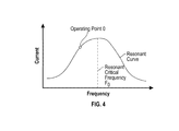
- FIG. 4 is an illustration of a resonant curve and an operating point of the resonant driver shown in FIGS. 1 and 2 ;
- FIG. 5 is an alternative embodiment of the circuit diagram shown in FIG. 2 , where the rectifier does not include fast recovery diodes;
- FIG. 6 is another embodiment of the circuit diagram shown in FIG. 5 , where the location of a blocking capacitor is modified.
- FIG. 1 is an exemplary block diagram of a circuit 10 for providing DC current to a load 18 .
- the driver circuit 10 may include a pair of power input lines 20 for connection to a source (not shown) of AC power such as, for example, main power lines at a nominal 120 volts AC.
- the driver circuit 10 may also include a resistor R 1 (shown in FIG. 2 ), an electromagnetic interference (EMI) filter 24 , a rectifier 26 , a voltage bus filter 27 , a start-up circuit 28 , a switch 30 , a transformer 32 , a switch 34 , a feedback circuit 35 , a resonant driver circuit 36 , a high-frequency DC rectifier 40 , and a blocking capacitor 46 .
- the circuit 10 provides substantially constant DC current to the load 18 , while maintaining a relatively high power factor (PF).
- the circuit 10 may include a PF of at least 0.7.
- the input lines 20 of the driver circuit 10 may be in electrical communication with the EMI filter 24 .
- the EMI filter 24 may include an inductor L 1 and capacitors C 1 and C 2 (shown in FIG. 2 ).
- the rectifier 26 may be in electrical communication with the EMI filter 24 , and is configured to convert incoming AC power from the EMI filter 24 to a pulsing DC power.
- the rectifier 26 is a high-frequency bridge rectifier including four fast recovery diodes D 1 , D 2 , D 3 , D 4 .
- the fast recovery diodes D 1 -D 4 may have a response time of less than about 150 ns, however it is to be understood that this parameter is merely exemplary in nature, and that other types of fast recovery diodes may be used as well.
- the output of the rectifier 26 may be in electrical communication with the voltage bus filter 27 .
- the voltage bus filter 27 may include a capacitor C 3 .
- the capacitor C 3 may be an electrolytic capacitor that acts as a smoothing capacitor.
- the capacitor C 3 may be used to smoothen or reduce the amount of ripple in the DC power provided by the rectifier 26 such that relatively steady DC power may be provided to the remaining components within the circuit 10 (i.e., the start-up circuit 28 , the switch 30 , the transformer 32 , the switch 34 , the resonant driver circuit 36 , and the high-frequency DC rectifier 40 ).
- the feedback circuit 35 may be used to create a charge on the capacitor C 3 . Maintaining a charge on the capacitor C 3 further smoothens the DC power provided by the rectifier 26 , which in turns improves the PF of the circuit 10 .
- the voltage bus filter 27 may be in electrical communication with the start-up circuit 28 .
- the start-up circuit 28 may include resistors R 2 and R 3 , diode D 6 , diac D 7 , and capacitor C 6 .
- the diac D 7 is a diode that conducts current only after a breakover voltage, V BO , has been reached.
- the capacitor C 6 may be charged until the diac D 7 reaches the breakover voltage V BO .
- the diac D 7 may start to conduct current.
- the diac D 7 may be connected to and sends current to the switch 30 .
- the diode D 6 may be used to discharge the capacitor C 6 and to prevent the diac D 7 from firing again.
- the circuit 10 may include a lower switch 30 (labelled Q 2 ) and an upper switch 34 (labelled Q 1 ) connected in a cascade arrangement.
- the resistor R 3 may be used to provide bias to the lower switching element Q 2 .
- the switching element Q 2 is a bipolar junction transistor (BJT).
- BJT bipolar junction transistor
- a diode D 10 may be provided to limit negative voltage between a base B and an emitter E of the switching element Q 2 , which in turn increases efficiency.
- the switch 30 may be connected to the transformer 32 .
- the transformer 32 includes three windings, T 1 A, T 1 B, and TIC.
- the winding T 1 A may include an opposite polarity when compared to the winding T 1 B. This ensures that if the switching element Q 2 is turned on, another switching element Q 1 will not turn on at the same time.
- both the switches 30 , 32 , diodes D 9 , D 10 , resistors R 5 and R 6 , and the transformer 32 define a high-frequency oscillator 50 .
- the high-frequency oscillator 50 generates a high-frequency AC signal V IN (shown in FIG. 1 ).
- the high-frequency AC signal V IN may be an AC signal having a frequency of at least about 40 kilohertz (kHz).
- An output 42 (shown in FIG. 1 ) of the high-frequency oscillator 50 may be in electrical communication with the resonant driver circuit 36 .
- the upper switching element Q 1 may also be a BJT.
- a diode D 9 may be provided to limit negative voltage between a base B and an emitter E of the upper switching element Q 1 , which in turn increases efficiency.
- the switch 34 may be used to electrically connect the high-frequency oscillator 50 to the resonant drive circuit 36 .
- the resonant drive circuit 36 may include a capacitor C 7 connected in series with the winding T 1 C of the transformer 32 .
- the resonant drive circuit 36 may also include an inductor L 2 .
- the resonant drive circuit 36 may be used to limit the current of the high-frequency AC signal V IN received from the high-frequency oscillator 50 .
- the resonant drive circuit 36 also produces a limited output voltage V LIMITED (shown in FIG. 1 ) based on the high-frequency AC signal V IN .
- the resonant driver circuit 36 may be in electrical communication with the high-frequency DC rectifier 40 .
- the limited output voltage V LIMITED created by the resonant driver 36 may be sent to the high-frequency DC rectifier 40 , and is rectified into a DC output voltage V DC (shown in FIG. 1 ).
- the DC output voltage V DC includes a substantially constant current that is supplied to the load 18 .
- the high-frequency DC rectifier 40 is a full wave rectifier including four diodes D 11 -D 14 and a filter capacitor C 8 .
- the full-wave rectifier may be connected in parallel with the filter capacitor C 8 .
- the diodes D 11 -D 14 may be low voltage diodes.
- the filter capacitor C 8 may be relatively small in size.
- the filter capacitor C 8 may be less than one microfarad.
- the blocking capacitor 46 may include a capacitor C 4 .
- the capacitor C 4 is in electrical communication with the rectifier 26 , the voltage bus filter 27 , and the high-frequency DC rectifier 40 .
- the capacitor C 4 may be used for impedance matching and for blocking DC current.
- the capacitor C 4 allows for the high-frequency AC signal V IN (shown in FIG. 1 ) generated by the high-frequency oscillator to flow to the high-frequency DC rectifier 40 .
- the capacitor C 4 also blocks the DC output voltage V DC generated by the high-frequency DC rectifier 40 located on the right side of the circuit 10 from flowing back to the rectifier 26 .
- the blocking capacitor C 4 is located between the rectifier 26 and the high-frequency DC rectifier 40 .
- the blocking capacitor 46 may be connected to the emitter E of the switch 30 .
- the feedback circuit 35 may be connected to the circuit 10 between the EMI filter 24 and the rectifier 26 .
- the feedback circuit 35 may also be connected to the high-frequency DC rectifier 40 .
- the feedback circuit 35 includes a capacitor C 5 , which acts as a charge pump that maintains a charge on the capacitor C 3 of the voltage bus filter 27 , which in turn increases the PF of the circuit 10 .
- FIG. 3 an exemplary illustration of an AC waveform A received by the inputs 20 of the circuit 10 is shown.
- FIG. 3 also illustrates a rectified input voltage V REC of the circuit 10 , which is measured after the rectifier 24 at the capacitor C 3 of the voltage bus filter 27 .
- the rectified input voltage V REC is based on the AC waveform received by the inputs 20 of the circuit 10 .
- the rectified input voltage V REC includes ripples R. It is to be understood that the amplitude of the ripples R of the rectified input voltage V REC may be reduced due to the feedback circuit 35 maintaining a charge on the capacitor C 3 of the voltage bus filter 27 . In other words, maintaining a charge on the capacitor C 3 will in turn further smoothen or reduce the amount of ripple in the rectified input voltage V REC through each half cycle of the AC waveform A at the inputs 20 of the circuit 10 (the half cycles of the AC waveform A are labelled in FIG. 3 ). Moreover, maintaining a charge on the capacitor C 3 will also result in increased conduction time of the current at the inputs 20 of the circuit 10 . Accordingly, the feedback circuit 35 may improve the overall PF of the circuit 10 . For example, in one embodiment, the overall PF of the circuit 10 may be at least 0.7.
- the load 18 may be one or more light emitting diodes (LEDs).
- the circuit 10 may include a pair of output terminals 44 that connect to a LED (not shown).
- the driver circuit 10 is used in a non-dimmable LED application.
- the load 18 may be any type of device that requires a substantially constant current during operation.
- the load 18 may be a heating element.
- FIG. 4 is an illustration of an exemplary resonance curve of the resonant drive circuit 36 shown in FIG. 2 .
- the resonance curve may include an operating point O and a resonant critical frequency f o .
- the critical frequency f o is located at a peak of the resonance curve, and the operating point O is located to the left of the critical frequency f o .
- increasing the capacitance of the capacitor C 7 or the inductance of the inductor L 2 of the resonant driver 36 may shift the critical frequency f o to the left, and decrease the capacitance of the capacitor C 7 or the inductance of the inductor L 2 may shift the critical frequency f o to the right.
- the frequency of oscillation of the resonance curve may be determined by winding T 1 C of the transformer 32 , resistors R 5 and R 6 , the upper switching element Q 1 , and the lower switching element Q 2 .
- the frequency of oscillation of the resonance curve may be based upon a number of the turns of the winding T 1 C of the transformer 32 , as well as the storage times of the upper switching element Q 1 and the lower switching element Q 2 .
- the inductance of the inductor L 2 as well as the capacitance of the capacitors C 4 and C 7 may be key factors in maintaining acceptable line regulation of the circuit 10 . Specifically, as line voltage increases a frequency of operation of the circuit 10 decreases. Moreover, the impedance of the inductor L 2 may decrease as the frequency of operation decreases, thereby causing an increase in current that is delivered to the load 18 ( FIG. 1 ). Thus, the inductance of the inductor L 2 as well as the capacitance of the capacitors C 7 and the capacitor C 4 may be selected such that an overall gain of the circuit 10 decreases as the frequency of operation decreases. This in turn may substantially decreases or minimize any increase in current that is delivered to the load 18 as the line voltage increases.
- FIG. 5 is an illustration of an alternative circuit 100 .
- the circuit 100 includes similar components as the circuit 10 shown in FIG. 2 . However, the circuit 100 also includes two additional diodes D 15 and D 16 that are located after the rectifier 26 . In the embodiment as shown in FIG. 5 , the diodes D 15 , D 16 are fast recovery diodes. Diode D 15 may be located between the rectifier 26 and diode D 16 . Diode D 16 may be located between diode D 15 and the high-frequency DC rectifier 40 . Since the circuit 100 includes fast recovery diodes D 15 and D 15 , the diodes D 1 -D 4 of the rectifier 26 do not need to be fast recovery diodes as well. In other words, the rectifier 26 is a standard bridge rectifier. Accordingly, the circuit 100 shown in FIG. 5 may result in a reduced number of fast recovery diodes when compared to the circuit 10 shown in FIG. 10 .
- FIG. 6 is yet another embodiment of a circuit 200 .
- the circuit 200 includes similar components as the circuit 100 shown in FIG. 5 .
- the location of the blocking capacitor C 4 has been modified. Specifically, the blocking capacitor C 4 is now connected between diode D 15 and the resonant driver circuit 36 .
- the location of the capacitor C 5 of the feedback circuit 35 has also been modified. Specifically, the capacitor C 5 is now located in parallel with the diode D 16 .
- capacitor C 5 still acts as a charge pump to maintain the charge on the capacitor C 3 of the voltage bus filter 27 .
- An additional capacitor C 11 has been added to the circuit 200 , and is in parallel with the capacitor C 3 of the voltage bus filter 27 .
- the capacitor C 11 acts as a divider.
- the disclosed circuit as illustrated in FIGS. 1-6 and described above provides a relatively low-cost and efficient approach for driving a load, while at the same time providing a relatively high PF (i.e., above 0.7).
- the disclosed circuit provides a relatively high PF without the need for active circuitry, which adds cost and complexity to an LED lighting fixture.
- the disclosed circuit also provides a relatively low-cost and efficient approach for delivering substantially constant current to a load as well.
- the disclosed circuit results in fewer components and a simpler design when compared to some types of LED drivers currently available on the market today.
Landscapes
- Engineering & Computer Science (AREA)
- Power Engineering (AREA)
- Circuit Arrangement For Electric Light Sources In General (AREA)
- Circuit Arrangements For Discharge Lamps (AREA)
- Led Devices (AREA)
- Dc-Dc Converters (AREA)
- Rectifiers (AREA)
Priority Applications (8)
| Application Number | Priority Date | Filing Date | Title |
|---|---|---|---|
| US14/594,536 US9531255B2 (en) | 2015-01-12 | 2015-01-12 | Low-cost driver circuit with improved power factor |
| US14/631,175 US20160205733A1 (en) | 2015-01-12 | 2015-02-25 | Low-cost dimming driver circuit with improved power factor |
| PCT/US2016/012255 WO2016114953A2 (en) | 2015-01-12 | 2016-01-06 | Low-cost dimming driver circuit with improved power factor |
| CA2968591A CA2968591C (en) | 2015-01-12 | 2016-01-06 | Low-cost driver circuit with improved power factor |
| PCT/US2016/012257 WO2016114954A1 (en) | 2015-01-12 | 2016-01-06 | Low-cost driver circuit with improved power factor |
| CN201680004417.2A CN107113954B (zh) | 2015-01-12 | 2016-01-06 | 具有改进的功率因数的低成本驱动器电路 |
| JP2017536943A JP2018505638A (ja) | 2015-01-12 | 2016-01-06 | 改善された力率を有する低コストドライバ回路 |
| GB1707659.7A GB2547376B (en) | 2015-01-12 | 2016-01-06 | Low-cost driver circuit with improved power factor |
Applications Claiming Priority (1)
| Application Number | Priority Date | Filing Date | Title |
|---|---|---|---|
| US14/594,536 US9531255B2 (en) | 2015-01-12 | 2015-01-12 | Low-cost driver circuit with improved power factor |
Related Child Applications (1)
| Application Number | Title | Priority Date | Filing Date |
|---|---|---|---|
| US14/631,175 Continuation-In-Part US20160205733A1 (en) | 2015-01-12 | 2015-02-25 | Low-cost dimming driver circuit with improved power factor |
Publications (2)
| Publication Number | Publication Date |
|---|---|
| US20160204692A1 US20160204692A1 (en) | 2016-07-14 |
| US9531255B2 true US9531255B2 (en) | 2016-12-27 |
Family
ID=56368230
Family Applications (1)
| Application Number | Title | Priority Date | Filing Date |
|---|---|---|---|
| US14/594,536 Active US9531255B2 (en) | 2015-01-12 | 2015-01-12 | Low-cost driver circuit with improved power factor |
Country Status (6)
| Country | Link |
|---|---|
| US (1) | US9531255B2 (zh) |
| JP (1) | JP2018505638A (zh) |
| CN (1) | CN107113954B (zh) |
| CA (1) | CA2968591C (zh) |
| GB (1) | GB2547376B (zh) |
| WO (1) | WO2016114954A1 (zh) |
Families Citing this family (3)
| Publication number | Priority date | Publication date | Assignee | Title |
|---|---|---|---|---|
| US9693403B2 (en) * | 2014-01-02 | 2017-06-27 | Philips Lighting Holding B.V. | Lighting arrangement |
| US9825552B1 (en) * | 2016-09-13 | 2017-11-21 | Kabushiki Kaisha Toshiba | Power conversion apparatus |
| US9973078B2 (en) * | 2016-09-13 | 2018-05-15 | Kabushiki Kaisha Toshiba | Power conversion apparatus and method of using the apparatus |
Citations (30)
| Publication number | Priority date | Publication date | Assignee | Title |
|---|---|---|---|---|
| US4672300A (en) * | 1985-03-29 | 1987-06-09 | Braydon Corporation | Direct current power supply using current amplitude modulation |
| US4782268A (en) * | 1986-04-07 | 1988-11-01 | Patent Treuhand Gesellschaft Fur Elektrische Gluhlampen Mbh | Low-pressure discharge lamp, particularly fluorescent lamp high-frequency operating circuit with low-power network interference |
| US4823250A (en) | 1987-11-05 | 1989-04-18 | Picker International, Inc. | Electronic control for light weight, portable x-ray system |
| US5404082A (en) | 1993-04-23 | 1995-04-04 | North American Philips Corporation | High frequency inverter with power-line-controlled frequency modulation |
| US5426344A (en) * | 1990-08-31 | 1995-06-20 | Ultralite International Pty Limited | Electronic ballasts |
| US5559395A (en) | 1995-03-31 | 1996-09-24 | Philips Electronics North America Corporation | Electronic ballast with interface circuitry for phase angle dimming control |
| US5691606A (en) * | 1994-09-30 | 1997-11-25 | Pacific Scientific Company | Ballast circuit for fluorescent lamp |
| US5914572A (en) | 1997-06-19 | 1999-06-22 | Matsushita Electric Works, Ltd. | Discharge lamp driving circuit having resonant circuit defining two resonance modes |
| US5925985A (en) | 1996-07-27 | 1999-07-20 | Singapore Productivity And Standards Board | Electronic ballast circuit for igniting, supplying and dimming a gas discharge lamp |
| US6144169A (en) | 1998-12-29 | 2000-11-07 | Philips Electronics North America Corporation | Triac dimmable electronic ballast with single stage feedback power factor inverter |
| US6175195B1 (en) | 1997-04-10 | 2001-01-16 | Philips Electronics North America Corporation | Triac dimmable compact fluorescent lamp with dimming interface |
| US6339298B1 (en) | 2000-05-15 | 2002-01-15 | General Electric Company | Dimming ballast resonant feedback circuit |
| US6348767B1 (en) * | 2000-10-25 | 2002-02-19 | General Electric Company | Electronic ballast with continued conduction of line current |
| US6442051B1 (en) | 2000-10-31 | 2002-08-27 | General Electric Company | Full thyristor bridge circuit with free wheeling diode for de-excitation control and stability sensing |
| US20030015479A1 (en) * | 1999-06-21 | 2003-01-23 | Kuennen Roy W. | Inductively coupled ballast circuit |
| US6833678B2 (en) | 2002-09-04 | 2004-12-21 | Patent Treuhand Gesellschaft Fur Elektrische Gluhlampen Mbh | Circuit arrangement for operating discharge lamps |
| US6870326B1 (en) * | 2001-04-06 | 2005-03-22 | Carlile R. Stevens | Fluorescent ballast with isolated system interface |
| US20050122057A1 (en) | 2003-12-05 | 2005-06-09 | Timothy Chen | Universal platform for phase dimming discharge lighting ballast and lamp |
| US20070152642A1 (en) * | 2006-01-03 | 2007-07-05 | Franklin Philip G | Wireless glass-mounted lighting fixtures |
| US20080074910A1 (en) | 2006-09-27 | 2008-03-27 | General Electric | Thyristor power converter filter for excitation applications |
| US20080088251A1 (en) * | 2006-09-30 | 2008-04-17 | Osram Sylvania, Inc. | Electronic Ballast with Improved Inverter Startup Circuit |
| US20100097000A1 (en) | 2008-10-16 | 2010-04-22 | General Electric Company | Low cost compact size single stage high power factor circuit for discharge lamps |
| US7750580B2 (en) * | 2006-10-06 | 2010-07-06 | U Lighting Group Co Ltd China | Dimmable, high power factor ballast for gas discharge lamps |
| US20100225239A1 (en) * | 2009-03-04 | 2010-09-09 | Purespectrum, Inc. | Methods and apparatus for a high power factor, high efficiency, dimmable, rapid starting cold cathode lighting ballast |
| US20100237799A1 (en) | 2009-03-23 | 2010-09-23 | Samsung Electro-Mechanics Co., Ltd. | Led driving circuit |
| US20110101880A1 (en) * | 2009-11-04 | 2011-05-05 | International Rectifier Corporation | Driver circuit with an increased power factor |
| US20120001562A1 (en) * | 1999-06-21 | 2012-01-05 | Access Business Group International Llc | Inductively coupled ballast circuit |
| US20130113382A1 (en) | 2011-11-04 | 2013-05-09 | Omron Corporation | Solid state relay and load drive circuit |
| US20130187557A1 (en) | 2012-01-19 | 2013-07-25 | Timothy Chen | Multi-level adaptive control circuitry for deep phase-cut dimming compact fluorescent lamp |
| US20150342004A1 (en) | 2014-05-22 | 2015-11-26 | Cree, Inc. | Lighting apparatus with inductor current limiting for noise reduction |
-
2015
- 2015-01-12 US US14/594,536 patent/US9531255B2/en active Active
-
2016
- 2016-01-06 JP JP2017536943A patent/JP2018505638A/ja active Pending
- 2016-01-06 CA CA2968591A patent/CA2968591C/en active Active
- 2016-01-06 GB GB1707659.7A patent/GB2547376B/en active Active
- 2016-01-06 WO PCT/US2016/012257 patent/WO2016114954A1/en active Application Filing
- 2016-01-06 CN CN201680004417.2A patent/CN107113954B/zh active Active
Patent Citations (33)
| Publication number | Priority date | Publication date | Assignee | Title |
|---|---|---|---|---|
| US4672300A (en) * | 1985-03-29 | 1987-06-09 | Braydon Corporation | Direct current power supply using current amplitude modulation |
| US4782268A (en) * | 1986-04-07 | 1988-11-01 | Patent Treuhand Gesellschaft Fur Elektrische Gluhlampen Mbh | Low-pressure discharge lamp, particularly fluorescent lamp high-frequency operating circuit with low-power network interference |
| US4823250A (en) | 1987-11-05 | 1989-04-18 | Picker International, Inc. | Electronic control for light weight, portable x-ray system |
| US5426344A (en) * | 1990-08-31 | 1995-06-20 | Ultralite International Pty Limited | Electronic ballasts |
| US5426344B1 (en) * | 1990-08-31 | 1996-12-31 | Ultralite International Pty Li | Electronic ballasts |
| US5404082A (en) | 1993-04-23 | 1995-04-04 | North American Philips Corporation | High frequency inverter with power-line-controlled frequency modulation |
| US5691606A (en) * | 1994-09-30 | 1997-11-25 | Pacific Scientific Company | Ballast circuit for fluorescent lamp |
| US5559395A (en) | 1995-03-31 | 1996-09-24 | Philips Electronics North America Corporation | Electronic ballast with interface circuitry for phase angle dimming control |
| US5925985A (en) | 1996-07-27 | 1999-07-20 | Singapore Productivity And Standards Board | Electronic ballast circuit for igniting, supplying and dimming a gas discharge lamp |
| US6175195B1 (en) | 1997-04-10 | 2001-01-16 | Philips Electronics North America Corporation | Triac dimmable compact fluorescent lamp with dimming interface |
| US5914572A (en) | 1997-06-19 | 1999-06-22 | Matsushita Electric Works, Ltd. | Discharge lamp driving circuit having resonant circuit defining two resonance modes |
| US6144169A (en) | 1998-12-29 | 2000-11-07 | Philips Electronics North America Corporation | Triac dimmable electronic ballast with single stage feedback power factor inverter |
| US20030015479A1 (en) * | 1999-06-21 | 2003-01-23 | Kuennen Roy W. | Inductively coupled ballast circuit |
| US20120001562A1 (en) * | 1999-06-21 | 2012-01-05 | Access Business Group International Llc | Inductively coupled ballast circuit |
| US6339298B1 (en) | 2000-05-15 | 2002-01-15 | General Electric Company | Dimming ballast resonant feedback circuit |
| US6348767B1 (en) * | 2000-10-25 | 2002-02-19 | General Electric Company | Electronic ballast with continued conduction of line current |
| US6442051B1 (en) | 2000-10-31 | 2002-08-27 | General Electric Company | Full thyristor bridge circuit with free wheeling diode for de-excitation control and stability sensing |
| US6870326B1 (en) * | 2001-04-06 | 2005-03-22 | Carlile R. Stevens | Fluorescent ballast with isolated system interface |
| US6833678B2 (en) | 2002-09-04 | 2004-12-21 | Patent Treuhand Gesellschaft Fur Elektrische Gluhlampen Mbh | Circuit arrangement for operating discharge lamps |
| US7075251B2 (en) | 2003-12-05 | 2006-07-11 | General Electric Company | Universal platform for phase dimming discharge lighting ballast and lamp |
| US20050122057A1 (en) | 2003-12-05 | 2005-06-09 | Timothy Chen | Universal platform for phase dimming discharge lighting ballast and lamp |
| US20070152642A1 (en) * | 2006-01-03 | 2007-07-05 | Franklin Philip G | Wireless glass-mounted lighting fixtures |
| US20080074910A1 (en) | 2006-09-27 | 2008-03-27 | General Electric | Thyristor power converter filter for excitation applications |
| US20080088251A1 (en) * | 2006-09-30 | 2008-04-17 | Osram Sylvania, Inc. | Electronic Ballast with Improved Inverter Startup Circuit |
| US7750580B2 (en) * | 2006-10-06 | 2010-07-06 | U Lighting Group Co Ltd China | Dimmable, high power factor ballast for gas discharge lamps |
| US7923941B2 (en) * | 2008-10-16 | 2011-04-12 | General Electric Company | Low cost compact size single stage high power factor circuit for discharge lamps |
| US20100097000A1 (en) | 2008-10-16 | 2010-04-22 | General Electric Company | Low cost compact size single stage high power factor circuit for discharge lamps |
| US20100225239A1 (en) * | 2009-03-04 | 2010-09-09 | Purespectrum, Inc. | Methods and apparatus for a high power factor, high efficiency, dimmable, rapid starting cold cathode lighting ballast |
| US20100237799A1 (en) | 2009-03-23 | 2010-09-23 | Samsung Electro-Mechanics Co., Ltd. | Led driving circuit |
| US20110101880A1 (en) * | 2009-11-04 | 2011-05-05 | International Rectifier Corporation | Driver circuit with an increased power factor |
| US20130113382A1 (en) | 2011-11-04 | 2013-05-09 | Omron Corporation | Solid state relay and load drive circuit |
| US20130187557A1 (en) | 2012-01-19 | 2013-07-25 | Timothy Chen | Multi-level adaptive control circuitry for deep phase-cut dimming compact fluorescent lamp |
| US20150342004A1 (en) | 2014-05-22 | 2015-11-26 | Cree, Inc. | Lighting apparatus with inductor current limiting for noise reduction |
Non-Patent Citations (6)
| Title |
|---|
| PCT, International Search Report and Written Opinion, International Application No. PCT/US2016/012257 (Mar. 30, 2016). |
| PCT/US2016/012255, International Search Report and Written Opinion, Jul. 26, 2016, 21 pages. |
| U.S. Appl. No. 14/631,175, Advisory Action, Jul. 29, 2016, 7 pages. |
| U.S. Appl. No. 14/631,175, Final Office Action, May 17, 2016, 25 pages. |
| U.S. Appl. No. 14/631,175, Interview Summary, Aug. 4, 2016, 5 pages. |
| US, Non-Final Office Action; U.S. Appl. No. 14/631,175; (Jan. 15, 2016). |
Also Published As
| Publication number | Publication date |
|---|---|
| US20160204692A1 (en) | 2016-07-14 |
| GB2547376A (en) | 2017-08-16 |
| GB2547376B (en) | 2019-03-27 |
| JP2018505638A (ja) | 2018-02-22 |
| CA2968591A1 (en) | 2017-07-21 |
| CN107113954B (zh) | 2019-07-02 |
| WO2016114954A1 (en) | 2016-07-21 |
| CA2968591C (en) | 2021-07-20 |
| CN107113954A (zh) | 2017-08-29 |
| GB201707659D0 (en) | 2017-06-28 |
Similar Documents
| Publication | Publication Date | Title |
|---|---|---|
| US9220159B2 (en) | Electronic ballast | |
| US8896221B2 (en) | Lighting device for semiconductor light emitting element and illumination apparatus including same | |
| JP6031669B2 (ja) | 低出力照明ユニットを動作させる回路装置及びそれを動作させる方法 | |
| US9544962B2 (en) | Driver device and driving method for driving an LED unit | |
| US20090295300A1 (en) | Methods and apparatus for a dimmable ballast for use with led based light sources | |
| US10790762B2 (en) | Relating to power adaptors | |
| WO1995010930A1 (en) | Integrated electronic energy converter | |
| US8569973B2 (en) | Power supply for lamps, particularly for LED-MR16 lamps | |
| JP6145980B2 (ja) | 照明装置 | |
| US20090128057A1 (en) | Fluorescent lamp and ballast with balanced energy recovery pump | |
| US9531255B2 (en) | Low-cost driver circuit with improved power factor | |
| US20160205733A1 (en) | Low-cost dimming driver circuit with improved power factor | |
| US9717121B2 (en) | Lighting device suitable for multiple voltage sources | |
| US9270196B2 (en) | Low-cost self-oscillating driver circuit | |
| TWI602470B (zh) | 多燈管型態螢光燈/發光二極體燈通用型照明驅動電路 | |
| US9736894B2 (en) | Improvements relating to power adaptors | |
| US8963447B2 (en) | Ballast with current control circuit | |
| US8547029B2 (en) | Dimmable instant start ballast |
Legal Events
| Date | Code | Title | Description |
|---|---|---|---|
| AS | Assignment |
Owner name: TECHNICAL CONSUMER PRODUCTS, INC., OHIO Free format text: ASSIGNMENT OF ASSIGNORS INTEREST;ASSIGNORS:CHEN, TIMOTHY;HAAS, DANIEL ALBERT;REEL/FRAME:035173/0825 Effective date: 20150113 |
|
| STCF | Information on status: patent grant |
Free format text: PATENTED CASE |
|
| CC | Certificate of correction | ||
| AS | Assignment |
Owner name: ENCINA BUSINESS CREDIT, LLC, AS AGENT, ILLINOIS Free format text: SECURITY INTEREST;ASSIGNOR:TECHNICAL CONSUMER PRODUCTS, INC.;REEL/FRAME:045681/0658 Effective date: 20180323 |
|
| AS | Assignment |
Owner name: TECHNICAL CONSUMER PRODUCTS, INC., OHIO Free format text: RELEASE BY SECURED PARTY;ASSIGNOR:PNC BANK, NATIONAL ASSOCIATION, AS AGENT;REEL/FRAME:045726/0793 Effective date: 20180323 |
|
| MAFP | Maintenance fee payment |
Free format text: PAYMENT OF MAINTENANCE FEE, 4TH YEAR, LARGE ENTITY (ORIGINAL EVENT CODE: M1551); ENTITY STATUS OF PATENT OWNER: LARGE ENTITY Year of fee payment: 4 |