US9525303B2 - Wireless charger circuit and method - Google Patents
Wireless charger circuit and method Download PDFInfo
- Publication number
- US9525303B2 US9525303B2 US15/000,940 US201615000940A US9525303B2 US 9525303 B2 US9525303 B2 US 9525303B2 US 201615000940 A US201615000940 A US 201615000940A US 9525303 B2 US9525303 B2 US 9525303B2
- Authority
- US
- United States
- Prior art keywords
- terminal
- interface
- receiver
- charged
- circuit
- Prior art date
- Legal status (The legal status is an assumption and is not a legal conclusion. Google has not performed a legal analysis and makes no representation as to the accuracy of the status listed.)
- Expired - Fee Related
Links
- 238000000034 method Methods 0.000 title claims 15
- 238000004891 communication Methods 0.000 claims description 15
- 230000005540 biological transmission Effects 0.000 claims description 4
- 230000008878 coupling Effects 0.000 claims description 4
- 238000010168 coupling process Methods 0.000 claims description 4
- 238000005859 coupling reaction Methods 0.000 claims description 4
- 238000010295 mobile communication Methods 0.000 claims 8
- 238000001514 detection method Methods 0.000 abstract description 9
- 230000001413 cellular effect Effects 0.000 description 15
- 238000010586 diagram Methods 0.000 description 8
- 230000001939 inductive effect Effects 0.000 description 7
- 230000004044 response Effects 0.000 description 6
- 230000005672 electromagnetic field Effects 0.000 description 5
- 230000006698 induction Effects 0.000 description 4
- 230000009471 action Effects 0.000 description 3
- 230000002159 abnormal effect Effects 0.000 description 2
- 238000010438 heat treatment Methods 0.000 description 2
- 230000001965 increasing effect Effects 0.000 description 2
- 230000002457 bidirectional effect Effects 0.000 description 1
- 238000005516 engineering process Methods 0.000 description 1
- 230000010354 integration Effects 0.000 description 1
- 230000002452 interceptive effect Effects 0.000 description 1
- 238000004519 manufacturing process Methods 0.000 description 1
- 238000012986 modification Methods 0.000 description 1
- 230000004048 modification Effects 0.000 description 1
- 238000012544 monitoring process Methods 0.000 description 1
- 230000001681 protective effect Effects 0.000 description 1
- 230000005180 public health Effects 0.000 description 1
- 230000009467 reduction Effects 0.000 description 1
Images


Classifications
-
- H02J7/025—
-
- H—ELECTRICITY
- H02—GENERATION; CONVERSION OR DISTRIBUTION OF ELECTRIC POWER
- H02J—CIRCUIT ARRANGEMENTS OR SYSTEMS FOR SUPPLYING OR DISTRIBUTING ELECTRIC POWER; SYSTEMS FOR STORING ELECTRIC ENERGY
- H02J7/00—Circuit arrangements for charging or depolarising batteries or for supplying loads from batteries
- H02J7/0042—Circuit arrangements for charging or depolarising batteries or for supplying loads from batteries characterised by the mechanical construction
- H02J7/0044—Circuit arrangements for charging or depolarising batteries or for supplying loads from batteries characterised by the mechanical construction specially adapted for holding portable devices containing batteries
-
- H—ELECTRICITY
- H02—GENERATION; CONVERSION OR DISTRIBUTION OF ELECTRIC POWER
- H02J—CIRCUIT ARRANGEMENTS OR SYSTEMS FOR SUPPLYING OR DISTRIBUTING ELECTRIC POWER; SYSTEMS FOR STORING ELECTRIC ENERGY
- H02J7/00—Circuit arrangements for charging or depolarising batteries or for supplying loads from batteries
- H02J7/02—Circuit arrangements for charging or depolarising batteries or for supplying loads from batteries for charging batteries from ac mains by converters
-
- H—ELECTRICITY
- H04—ELECTRIC COMMUNICATION TECHNIQUE
- H04B—TRANSMISSION
- H04B1/00—Details of transmission systems, not covered by a single one of groups H04B3/00 - H04B13/00; Details of transmission systems not characterised by the medium used for transmission
- H04B1/38—Transceivers, i.e. devices in which transmitter and receiver form a structural unit and in which at least one part is used for functions of transmitting and receiving
- H04B1/3827—Portable transceivers
- H04B1/3883—Arrangements for mounting batteries or battery chargers
-
- H—ELECTRICITY
- H04—ELECTRIC COMMUNICATION TECHNIQUE
- H04M—TELEPHONIC COMMUNICATION
- H04M1/00—Substation equipment, e.g. for use by subscribers
- H04M1/02—Constructional features of telephone sets
- H04M1/0202—Portable telephone sets, e.g. cordless phones, mobile phones or bar type handsets
-
- H—ELECTRICITY
- H01—ELECTRIC ELEMENTS
- H01M—PROCESSES OR MEANS, e.g. BATTERIES, FOR THE DIRECT CONVERSION OF CHEMICAL ENERGY INTO ELECTRICAL ENERGY
- H01M10/00—Secondary cells; Manufacture thereof
- H01M10/42—Methods or arrangements for servicing or maintenance of secondary cells or secondary half-cells
- H01M10/425—Structural combination with electronic components, e.g. electronic circuits integrated to the outside of the casing
- H01M10/4257—Smart batteries, e.g. electronic circuits inside the housing of the cells or batteries
-
- H02J2007/0098—
-
- Y—GENERAL TAGGING OF NEW TECHNOLOGICAL DEVELOPMENTS; GENERAL TAGGING OF CROSS-SECTIONAL TECHNOLOGIES SPANNING OVER SEVERAL SECTIONS OF THE IPC; TECHNICAL SUBJECTS COVERED BY FORMER USPC CROSS-REFERENCE ART COLLECTIONS [XRACs] AND DIGESTS
- Y02—TECHNOLOGIES OR APPLICATIONS FOR MITIGATION OR ADAPTATION AGAINST CLIMATE CHANGE
- Y02E—REDUCTION OF GREENHOUSE GAS [GHG] EMISSIONS, RELATED TO ENERGY GENERATION, TRANSMISSION OR DISTRIBUTION
- Y02E60/00—Enabling technologies; Technologies with a potential or indirect contribution to GHG emissions mitigation
- Y02E60/10—Energy storage using batteries
Definitions
- the present application relates to charging circuits for charging batteries in portable devices.
- wireless charger refers to a charger that does not connect to the device to be charged through a charging cable.
- direct contact chargers a charger or charging station (“charge base”) transfers energy through direct contacts to the device being charged.
- inductive chargers a charger transfers energy over an electromagnetic field that couples the charger to the portable device being charged.
- an inductive charger is provided in the form of a charge base, and energy is transferred by inductive coupling from the electromagnetic field generated by the charge base to an electrical circuit, which in turns charges the batteries of the portable device.
- An inductive charger typically has an induction coil which creates an alternating electromagnetic field from within the charge base.
- a second induction coil provided in the portable device, takes power from the electromagnetic field and converts it into an electrical current to charge the battery.
- the two induction coils in proximity effectively form an electrical transformer.
- This form of induction charging has many disadvantages not present in direct contact charging. For example, relative to direct contact chargers, inductive chargers have a lower efficiency and increased resistive heating. As energy that is lost turns into heat, an inductive charger can get quite warm during charging. An increase in temperature unduly increases stress to the battery, so that batteries that are charged in this manner may not last as long, as compared to batteries charged on a mat or through a regular plug-in charger.
- the heat buildup which occurs only during charging, represents a low efficiency that depends significantly on the relative position of the two inductively coupled coils. Implementations that use lower frequencies or older drive technologies charge more slowly and generate more heat. Unlike direct contact chargers, inductive chargers include drive electronics and coils, thus increasing complexity and manufacturing costs. Another disadvantage is a public health concern that the alternating electromagnetic field ( ⁇ 5 W, at radio frequencies in the 80-300 kHz range) is typically used very close to the human body. Some charge bases transmit at 915 MHz, which is the frequency that is used for food heating in microwave ovens.
- point-to-point electrodes such as those used in home cordless telephones.
- One disadvantage of point-to-point electrodes is device alignment (i.e., the charge base and the device being charged are required to be placed precisely aligned in position and in correct polarities).
- Another way uses multiple-point to strips, such as used in the Wildcharge system.
- the disadvantage is the device to be charged has to have multiple electrodes arranged in a small circle, which is usually provided at the weight center of the device to be charged to prevent tilting. If the device is tilted, electrical contact is lost and charging fails.
- Another disadvantage results from misaligned positions between the charge base and the device being charged (e.g., when two electrodes fall between two adjacent electrode strips).
- two or more conducting layers are provided on a charge base as electrodes, such that a portable device to be charged can be placed in any position without risking disconnection from one electrode.
- the device to be charged does not need to have more than two electrodes which also do not need to be placed at or near the weight center of the portable device.
- the two electrodes on the portable device to be charged can be placed anywhere on that device, so long as the distance between these electrodes is greater than the base electrode plate on the charge base.
- a charging system for a mobile device includes a transmitter and a receiver.
- the transmitter includes (a) a first interface to a power source having a first terminal and a second terminal; (b) a second interface to the receiver having a first terminal and a second terminal; (c) a polarity detection circuit coupled to the first and second terminals of the second interface for detecting polarities of the first and second terminals of the second interface; and (d) first and second switches controlled by the polarity detection circuit, wherein the first switch selectively connects the first terminal of the first interface to either the first terminal of the second interface or the second terminal of the second interface, and wherein the second switch selectively connects the first terminal of the first interface to either the first terminal of the second interface or the second terminal of the second interface.
- the receiver includes: (a) a first interface having a first terminal and a second terminal; (b) a second interface having a first terminal and a second terminal coupled to a device to be charged; and (c) a connection circuit between the first terminal of the first interface and the first terminal of the second interface, wherein the connection circuit is conductive when the voltage across the first terminal of the first interface and the second terminal of the first interface is of a first polarity, and the connection circuit is non-conductive when the voltage across the first terminal of the first interface and the second terminal of the first interface is of a second polarity opposite the first polarity.
- identification information is exchanged between the transmitter and the receiver.
- current is monitored throughout to prevent power transfer from the device to be charged and the charge base.
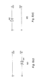
- FIG. 1 shows a charging configuration for charge base 109 , back cover 101 and portable cellular telephone 100 , in accordance with one embodiment of the present invention.
- FIG. 2 shows a reverse side of back cover 101 in relation to the reverse side of cellular telephone 100 (shown schematically), in accordance with one embodiment of the present invention.
- FIG. 3 shows schematically charge base 109 , in accordance with one embodiment of the present invention.
- FIG. 4 is a block diagram of a charger system including integrated circuit 120 in charge base 120 , integrated circuit 113 on back cover 101 and charger integrated circuit 121 in cellular telephone 100 , in accordance with one embodiment of the present invention.
- FIGS. 5( a )-5( d ) shows a 4-electrode charge base which can charge up to two cellular telephones.
- FIG. 7 shows flow-chart 700 summarizing operations of a transmitter side integrated circuit described above.
- FIG. 8( a ) is representative schematic circuit 800 for a receiver side integrated circuit, in accordance with one embodiment of the present invention.
- FIG. 8( b ) is representative schematic circuit 820 for a receiver side integrated circuit, in accordance with one embodiment of the present invention.
- FIG. 8( c ) is representative schematic circuit 840 for a receiver side integrated circuit, in accordance with one embodiment of the present invention.
- FIG. 8( d ) is representative schematic circuit 860 for a receiver side integrated circuit, in accordance with one embodiment of the present invention.
- FIG. 9( a ) is a block diagram of communication circuit 900 suitable for communicating information between the transmitter side (e.g., integrated circuit 120 of charge base 109 ) and the receiver side (e.g., integrated circuit 113 of back cover 101 ), in accordance with one embodiment of the present invention.
- the transmitter side e.g., integrated circuit 120 of charge base 109
- the receiver side e.g., integrated circuit 113 of back cover 101
- FIG. 9( b ) is a block diagram of communication circuit 920 suitable for communicating information between the transmitter side and the receiver side, using both terminals (i.e., VDD and GND) as signal paths, in accordance with one embodiment of the present invention.
- FIG. 1 shows a charging configuration for charge base 109 and portable cellular telephone 100 , in accordance with one embodiment of the present invention.
- planar electrodes 106 and 107 separated and insulated from each other by gap 108 .
- Cellular telephone 100 may be provided back cover 101 for attachment to the reverse side of cellular telephone 100 , as shown in FIG. 1 .
- conductive ring 102 On one side of back cover 101 is provided conductive ring 102 positioned around edge 104 over the outside perimeter of camera 114 (see FIG. 2 ), which is customarily provided on a smartphone.
- conductive plate 103 On the other side of back cover 101 is provided conductive plate 103 , which may also serve, for example, as a logo plate for cellular telephone 100 .
- conductive ring 102 and conductive plate 103 also serve as electrodes on cellular telephone 100 for contacting counterpart planar electrodes 106 and 107 of charge base 109 , as shown in FIG. 1 .
- Back cover 101 also includes connector 105 , which is provided to couple with power connector 110 of cellular telephone 100 (see FIG. 2 ).
- Power connector 110 is otherwise the receptacle for a charging cable that is used to charge cellular telephone 100 in conventional charging.
- FIG. 2 shows a reverse side of back cover 101 in relation to the reverse side of cellular telephone 100 (shown schematically), in accordance with one embodiment of the present invention.
- connector 105 is shown configured for coupling to power connector 110 .
- integrated circuit 113 (“receiver IC3”), which is electrically connected to conductive ring 102 , conductive plate 103 and connector 105 .
- a conductive path 112 (e.g., a wire) on back cover 101 .
- FIG. 2 also shows schematically battery 115 of cellular telephone 100 .
- FIG. 3 shows schematically charge base 109 , in accordance with one embodiment of the present invention.
- charge base 109 includes integrated circuit 120 (“auto switch and protection IC”), which is connected to planar electrodes 106 and 107 at conducting points 118 and 119 through conductive paths 116 and 117 (e.g., conductive wires), respectively.
- integrated circuit 120 may be powered, for example, by a USB source, a battery or a power adapter.
- FIG. 4 is a block diagram of a charge system including integrated circuit 120 in charge base 109 , integrated circuit 113 on back cover 101 and charger integrated circuit 121 in cellular telephone 100 , in accordance with one embodiment of the present invention.
- integrated circuit 120 includes switches S2 and S1, which are controlled by a polarity direction and protective circuit to configure the polarities at electrodes 106 and 107 .
- integrated circuit 120 is the “transmitter side” integrated circuit, which sends detection signals to electrodes 106 and 107 periodically to detect if a valid electronic device to be charged is placed on charge base 109 .
- the response by a valid device to be charged determines the polarity of the device's electrodes 102 and 103 contacting planar electrodes 106 and 107 .
- integrated circuit 120 turns on the corresponding power switches S2 and S1, thus connecting power supply V to electrodes 106 and 107 in proper polarity for charging the portable device.
- integrating circuit 120 also monitors the charge current in real time. When the charge current diminishes sufficiently, thus indicating that the charge is substantially complete, integrated circuit 120 sends out a “fully charged” indication. Also, after integrated circuit 120 connects power supply V to electrodes 106 and 107 through switches S2 and S1, integrated circuit 120 begins detecting in real time if the portable device being charge remains on charge base 109 .
- integrated circuit 120 When integrated circuit 120 detects the device being charged is removed from charge base 109 , integrated circuit 120 returns to idle status. In the idle state, integrated circuit 120 sends detection signals to electrodes 106 and 107 periodically until a valid device to be charged is detected as being placed on charge base 109 .
- integration circuit 120 in charge base 109 is configured to perform the following steps:
- integrated circuit 120 also monitors in real time whether or not the device being charged remains on charge base 109 .
- integrated circuit 120 disconnects power switches S1 and S2 electrically from power supply V, and returns to step (a) where charge base 109 determines whether or not a valid electronic device has been placed on charge base 109 .
- integrated circuit 120 also monitors the surrounding temperature; all power switches are disconnected from power supply V, when integrated circuit 120 detects a temperature that exceeds the preset threshold.
- Integrated circuit 113 may be built into or included as an accessory (e.g., back cover 101 ) to the device to be charged.
- Integrated circuit 113 may provide to the transmitter side (i.e., integrated circuit 120 ) information to validate the device to be charged and the polarities of its electrodes. Communicating through electrodes 102 , 103 , 106 and 107 , integrated circuit 113 provides identification information to integrated circuit 120 . As described above, after integrated circuit 120 determines that the device to be charged is an appropriate device, integrated circuit 120 provides a charging voltage at electrodes 106 and 107 to charge the battery inside the device being charged.
- integrated circuit 120 on the charge base 109 detects the polarities of the electrodes of the device to be charged that are contacting charge base 109 .
- the same principles may be applied for a charger having more than two charge electrodes, such as the 4-electrode charge base shown in FIGS. 5( a )-5( d ) .
- FIGS. 5( a )-5( d ) show a 4-electrode charge base which can accommodate up to two cellular telephones placed in various orientations.
- the use of multiple electrodes on a charge base provides greater charge flexibility and allows simultaneous charging of multiple devices.
- Various configurations, such as, 6, 8 or more electrodes can be easily provided.
- circuit 120 sends signals to the receiver side (e.g., integrated circuit 113 ) according to a hand-shaking protocol.
- the response from the receiver side provides identification information (e.g., device name and device model).
- Circuit 600 includes circuit 601 for detecting polarities of the device to be charged.
- switches 611 and 612 are provided to selectively connect electrodes 107 and 106 to power terminal VDD at clock phases ph1 and ph2. At the first phase (ph1), switch 611 on the “A” side is open and switch 612 on the “B” side is closed while electrode 107 is connected to VDD.
- the transmitter side i.e., integrated circuit 120
- the receiver side e.g., integrated circuit 113
- the receiver integrated circuit responds according to the hand-shake protocol.
- the hand-shaking protocol is implemented by a proprietary hand-shaking protocol that requires the conduction current to flow only from the positive terminal to the negative terminal of the device to be charged; and the reverse conduction current to be negligible.
- the valid receiver integrated circuit informs the transmitter integrated circuit that (1) it is the valid receiver, and (2) the proper polarities of its electrodes as currently placed on charge base 109 .
- the receiver integrated circuit sends back identification information through the contacting electrodes.
- integrated circuit 120 monitors the charge current passing through switches S1 and S2. When the charge current falls below the “charge finish” threshold, integrated circuit 120 initializes hand-shake detection to determine whether or not the current reduction is due to removal of the device being charged from charge base 109 or the device being charged remains on charge base 109 , but is approaching being fully charged. If Case 1 condition is detected at the output terminals of comparators 604 and 606 , the device being charged is removed. If the hand-shaking result shows Case 2 condition or Case 3 condition at the output terminals of comparators 604 and 606 , the device being charged is considered fully charged. Integrated circuit 120 reports the results accordingly.
- integrated circuit 120 also detects if the charge current is higher than an “over-current-protection” threshold. If the charge current exceeds the over-current protection threshold, integrated circuit 120 turns off the appropriate transistors of switches S1 and S2 to avoid damage to charge base 109 , and indicates the condition by turning on the corresponding fault condition light. In the same embodiment, abnormal conditions, such as an out-of-range temperature or voltage, are also monitored. If an abnormal condition is detected, integrated circuit 120 takes appropriate lock-out or shut-down actions.
- FIG. 7 shows flow-chart 700 summarizing operations of a transmitter side integrated circuit described above.
- FIG. 8( a ) is representative schematic circuit 800 for a receiver side integrated circuit, in accordance with one embodiment of the present invention.
- power-on reset circuit 801 causes comparator 802 to switch on transistor MN. If terminals 102 and 103 come into contact with a charge base (e.g., charge base 109 ) and if the hand-shaking signals are such that the voltage across terminals 102 and 103 is negative, comparator 802 turns off transistor MN to avoid imposing a negative voltage across the device to be charged.
- diode 803 provides additional protection.
- comparator 802 When the transmitter side provides the hand-shaking signals such that the voltage across terminals 102 and 103 is positive, comparator 802 turns on transistor MN to provide a positive voltage for charging across the device to be charged. In this manner, the conduction current is non-zero when a positive voltage is present from the “+” ( 102 ) terminal to the “ ⁇ ” ( 103 ) terminal, and the conduction current is negligible when the polarities are reversed, as required under the proprietary protocol discussed above.
- ID response module 804 obtains identification information from the device to be charged and provides the identification information to the transmitter side.
- transistor MN is fully conducting and internal comparator 802 compares the voltage between terminal “VSS” (at device being charged) and “ ⁇ ” ( 103 ) to monitor the channel current in transistor MN, to prevent power transfer from the device being charged to charge base 109 .
- FIG. 8( b ) shows exemplary schematic circuit 820 for a receiver side integrated circuit, in accordance with one embodiment of the present invention.
- Circuit 820 operates in substantially the same manner as described for circuit 800 of FIG. 8( a ) , except that transistor MP of circuit 820 is a p-channel MOS transistor, while transistor MN of circuit 800 is an N-channel MOS transistor.
- the communication protocol may be provided by a proprietary protocol without interfering with public communication signals.
- data communication can be achieved (but not necessarily) by modulating data symbols ( 911 ) under modulation scheme 912 (e.g., using a carrier signal) for transmission and demodulated ( 913 ) when received.
- Signal communication may be unidirectional at a time (i.e., from transmitter to receiver or from receiver to transmitter), or bidirectional simultaneously (i.e., from transmitter to receiver and from receiver to transmitter).
- FIG. 9( b ) is a block diagram of communication circuit 920 suitable for communicating information between the transmitter side and the receiver side, using both terminals (i.e., VDD and GND) as signal paths, in accordance with one embodiment of the present invention. Since both the VDD and GND terminals are in the communication paths, additional filters 923 and 924 are provided.
Abstract
A charging system for a mobile device includes a transmitter and a receiver. The transmitter includes (a) a first interface to a power source; (b) a second interface to the receiver; (c) a polarity detection circuit for detecting polarities of the; and (d) first and second switches controlled by the polarity detection circuit, wherein each switch selectively connects a terminal of the first interface to a terminal of the second interface. The receiver includes: (a) a first interface; (b) a second interface coupled to a device to be charged; and (c) a connection circuit between a terminal of the first interface and a terminal of the second interface, wherein the connection circuit is conductive when the voltage across these terminals is of a first polarity, and a second polarity otherwise.
Description
The present invention claims priority from, and is a divisional application of, U.S. patent application Ser. No. 13/734,610, filed on Jan. 4, 2013, which is incorporated herein by reference in its entirety as if fully set forth herein.
1. Field of the Invention
The present application relates to charging circuits for charging batteries in portable devices.
2. Discussion of the Related Art
There are two categories of wireless chargers for portable devices. In this regard, the term “wireless charger” refers to a charger that does not connect to the device to be charged through a charging cable. In one category, which is referred to herein as “direct contact chargers”, a charger or charging station (“charge base”) transfers energy through direct contacts to the device being charged. In the other category, which is referred to herein as “inductive chargers”, a charger transfers energy over an electromagnetic field that couples the charger to the portable device being charged. Typically, an inductive charger is provided in the form of a charge base, and energy is transferred by inductive coupling from the electromagnetic field generated by the charge base to an electrical circuit, which in turns charges the batteries of the portable device.
An inductive charger typically has an induction coil which creates an alternating electromagnetic field from within the charge base. A second induction coil, provided in the portable device, takes power from the electromagnetic field and converts it into an electrical current to charge the battery. The two induction coils in proximity effectively form an electrical transformer. This form of induction charging has many disadvantages not present in direct contact charging. For example, relative to direct contact chargers, inductive chargers have a lower efficiency and increased resistive heating. As energy that is lost turns into heat, an inductive charger can get quite warm during charging. An increase in temperature unduly increases stress to the battery, so that batteries that are charged in this manner may not last as long, as compared to batteries charged on a mat or through a regular plug-in charger. The heat buildup, which occurs only during charging, represents a low efficiency that depends significantly on the relative position of the two inductively coupled coils. Implementations that use lower frequencies or older drive technologies charge more slowly and generate more heat. Unlike direct contact chargers, inductive chargers include drive electronics and coils, thus increasing complexity and manufacturing costs. Another disadvantage is a public health concern that the alternating electromagnetic field (˜5 W, at radio frequencies in the 80-300 kHz range) is typically used very close to the human body. Some charge bases transmit at 915 MHz, which is the frequency that is used for food heating in microwave ovens.
There are many ways to implement direct contact charging. One way uses point-to-point electrodes, such as those used in home cordless telephones. One disadvantage of point-to-point electrodes is device alignment (i.e., the charge base and the device being charged are required to be placed precisely aligned in position and in correct polarities). Another way uses multiple-point to strips, such as used in the Wildcharge system. The disadvantage is the device to be charged has to have multiple electrodes arranged in a small circle, which is usually provided at the weight center of the device to be charged to prevent tilting. If the device is tilted, electrical contact is lost and charging fails. Another disadvantage results from misaligned positions between the charge base and the device being charged (e.g., when two electrodes fall between two adjacent electrode strips).
According to one embodiment of the present invention, two or more conducting layers are provided on a charge base as electrodes, such that a portable device to be charged can be placed in any position without risking disconnection from one electrode. As a result, the device to be charged does not need to have more than two electrodes which also do not need to be placed at or near the weight center of the portable device. The two electrodes on the portable device to be charged can be placed anywhere on that device, so long as the distance between these electrodes is greater than the base electrode plate on the charge base.
A charging system for a mobile device includes a transmitter and a receiver. The transmitter includes (a) a first interface to a power source having a first terminal and a second terminal; (b) a second interface to the receiver having a first terminal and a second terminal; (c) a polarity detection circuit coupled to the first and second terminals of the second interface for detecting polarities of the first and second terminals of the second interface; and (d) first and second switches controlled by the polarity detection circuit, wherein the first switch selectively connects the first terminal of the first interface to either the first terminal of the second interface or the second terminal of the second interface, and wherein the second switch selectively connects the first terminal of the first interface to either the first terminal of the second interface or the second terminal of the second interface. The receiver includes: (a) a first interface having a first terminal and a second terminal; (b) a second interface having a first terminal and a second terminal coupled to a device to be charged; and (c) a connection circuit between the first terminal of the first interface and the first terminal of the second interface, wherein the connection circuit is conductive when the voltage across the first terminal of the first interface and the second terminal of the first interface is of a first polarity, and the connection circuit is non-conductive when the voltage across the first terminal of the first interface and the second terminal of the first interface is of a second polarity opposite the first polarity.
According to one embodiment of the present invention, after the polarities of the device to be charged are determined, identification information is exchanged between the transmitter and the receiver. In one embodiment, current is monitored throughout to prevent power transfer from the device to be charged and the charge base.
The present invention is better understood upon consideration of the detailed description below in conjunction with the accompanying drawings.
Thus, to summarize, according to one embodiment of the present invention, integration circuit 120 in charge base 109 is configured to perform the following steps:
-
- (a) detecting (i) if there is any object placed on
charge base 109, (ii) if an object is detected, determining if the object is a valid electronic device, (iii) if the object is detected and the object is not a valid electronic device, outputting a signal indicating an error condition, and (iv) if an object is not detected, no action is taken; - (b) if a valid electronic device is detected, (i) sending an electrical stimulus signal through
planar electrodes planar electrodes planar electrodes - (c) after the polarities of the two electrodes of the device to be charged are determined, turning on power switches S2 and S1 within
integrated circuit 102 so that the output voltage acrossplanar electrodes - (d) through the output voltage imposed on
planar electrodes - (e) monitoring the progress of the charging operation and taking proper actions as the battery charging progresses, e.g., reducing the output current and send out a “fully charged” indication signal when the battery is fully charged.
- (a) detecting (i) if there is any object placed on
In one embodiment, integrated circuit 120 also monitors in real time whether or not the device being charged remains on charge base 109. When the device being charged is removed from charge base 109, integrated circuit 120 disconnects power switches S1 and S2 electrically from power supply V, and returns to step (a) where charge base 109 determines whether or not a valid electronic device has been placed on charge base 109.
In one embodiment, integrated circuit 120 also monitors the surrounding temperature; all power switches are disconnected from power supply V, when integrated circuit 120 detects a temperature that exceeds the preset threshold.
Another feature of integrated circuit 120 is the ability to communicate with integrated circuit 113 on back cover 101 using the connecting electrical paths of electrodes 102, 103, 106 and 107. This arrangement provides an internal signal communication system that does not require use of any public bandwidth, thus freeing bandwidth in the portable device for variable data communication, such as audio or video data.
Thus, as described above, integrated circuit 120 on the charge base 109 detects the polarities of the electrodes of the device to be charged that are contacting charge base 109. The same principles may be applied for a charger having more than two charge electrodes, such as the 4-electrode charge base shown in FIGS. 5(a)-5(d) . FIGS. 5(a)-5(d) show a 4-electrode charge base which can accommodate up to two cellular telephones placed in various orientations. The use of multiple electrodes on a charge base provides greater charge flexibility and allows simultaneous charging of multiple devices. Various configurations, such as, 6, 8 or more electrodes can be easily provided.
-
- Case 1: When no load is connected across
electrodes - Case 2: When there is a short circuit between “A” (107) and “B” (106), a valid “1” is detected in both phases, which is recognized as an invalid load.
- Case 3: When a device to be charged with a valid receiver integrated circuit (e.g., integrated circuit 113) is placed between terminal “A” (i.e., electrode 107) and terminal “B” (i.e., electrode 106) with the positive terminal touching terminal “A” (107) and the negative terminal touching terminal “B” (i.e., electrode 106), a valid “1” is obtained at
comparator 602 at phase ph1 and a valid “0” atcomparator 603 at phase ph2. This result is recognized as a valid load. Polarity detection may be repeated to confirm the result.Integrated circuit 120 then connects terminal “A” (107) to power terminal VDD (e.g., by turning on transistor PFET_A of switch S2) and terminal “B” (106) to ground terminal VSS (e.g., by turning on transistor NFET_B of switch S1). Charging can then begin. - Case 4: When the device to be charged with a valid receiver integrated circuit (e.g., integrated circuit 113) is placed between terminal “A” (i.e., electrode 107) and terminal “B” (i.e., electrode 106) with the negative terminal touching terminal “A” (107) and the positive terminal touching terminal “B” (i.e., electrode 106), a valid “0” is obtained at
comparator 602 at phase ph1 and a valid atcomparator 603 at phase ph2. This result is recognized as a valid load. Polarity detection may be repeated to confirm the result.Integrated circuit 120 then connects terminal “B” (106) to power terminal VDD (e.g., by turning on transistor PFET_B of switch S2) and terminal “A” (106) to ground terminal VSS (e.g., by turning on transistor NFET_A of switch S2). Charging can then begin.
- Case 1: When no load is connected across
Simultaneously, the transmitter side (i.e., integrated circuit 120) sends, according to the hand-shaking protocol, a command to the receiver side (e.g., integrated circuit 113) to obtain identification information. The receiver integrated circuit responds according to the hand-shake protocol. According to one embodiment of the present invention, the hand-shaking protocol is implemented by a proprietary hand-shaking protocol that requires the conduction current to flow only from the positive terminal to the negative terminal of the device to be charged; and the reverse conduction current to be negligible. Thus, the valid receiver integrated circuit informs the transmitter integrated circuit that (1) it is the valid receiver, and (2) the proper polarities of its electrodes as currently placed on charge base 109. In response to the transmitter's command, the receiver integrated circuit sends back identification information through the contacting electrodes.
After charging begins, integrated circuit 120 monitors the charge current passing through switches S1 and S2. When the charge current falls below the “charge finish” threshold, integrated circuit 120 initializes hand-shake detection to determine whether or not the current reduction is due to removal of the device being charged from charge base 109 or the device being charged remains on charge base 109, but is approaching being fully charged. If Case 1 condition is detected at the output terminals of comparators 604 and 606, the device being charged is removed. If the hand-shaking result shows Case 2 condition or Case 3 condition at the output terminals of comparators 604 and 606, the device being charged is considered fully charged. Integrated circuit 120 reports the results accordingly.
According to one embodiment of the present invention, integrated circuit 120 also detects if the charge current is higher than an “over-current-protection” threshold. If the charge current exceeds the over-current protection threshold, integrated circuit 120 turns off the appropriate transistors of switches S1 and S2 to avoid damage to charge base 109, and indicates the condition by turning on the corresponding fault condition light. In the same embodiment, abnormal conditions, such as an out-of-range temperature or voltage, are also monitored. If an abnormal condition is detected, integrated circuit 120 takes appropriate lock-out or shut-down actions.
During charging, transistor MN is fully conducting and internal comparator 802 compares the voltage between terminal “VSS” (at device being charged) and “−” (103) to monitor the channel current in transistor MN, to prevent power transfer from the device being charged to charge base 109.
The above detailed description is provided to illustrate the specific embodiments of the present invention and is not intended to be limiting. Numerous variations and modifications within the scope of the present invention are possible. The present invention is set forth in the following claims.
Claims (28)
1. In a charging system for a mobile device including a transmitter and a receiver, the receiver comprising:
a first interface having a first terminal and a second terminal;
a second interface having a first terminal and a second terminal coupled to a device to be charged;
a connection circuit between the first terminal of the first interface and the first terminal of the second interface, wherein the connection circuit is conductive when the voltage across the first terminal of the first interface and the second terminal of the first interface is of a first polarity, and the connection circuit is non-conductive when the voltage across the first terminal of the first interface and the second terminal of the first interface is of a second polarity opposite the first polarity.
2. The receiver of claim 1 , further comprises a diode connecting the first and second terminals of the second interface.
3. The receiver of claim 1 , wherein the connection circuit comprises a zener diode.
4. The receiver of claim 1 , wherein the connection circuit comprises a transistor.
5. The receiver of claim 4 , further comprising current sensing circuit that senses the channel current in the transistor wherein, when the channel current exceeds a predetermined threshold, the current sensing circuit turns off the transistor.
6. The receiver of claim 5 , wherein the current sensing circuit comprises a comparator that compares the voltage across the first terminal of the first interface and a voltage at the second terminal of the second interface.
7. The receiver of claim 1 , further comprising a communication circuit for providing data over the first and second terminals of the first interface.
8. The receiver of claim 7 , further comprising a modulation circuit for modulating data for transmission to the transmitter.
9. The receiver of claim 7 , further comprising a demodulation circuit for demodulating data received from the transmitter.
10. The receiver of claim 1 , wherein the receiver is provided a cover to be placed over the device to be charged.
11. The receiver of claim 10 , wherein the device to be charged comprises a mobile communication device.
12. The receiver of claim 11 , wherein the mobile communication device comprises a camera, wherein the first terminal of the first interface is provided as a conductive ring around the camera of the mobile communication device.
13. The receiver of claim 11 , wherein the second terminal of the second interface comprises a conductive name plate.
14. The receiver of claim 11 , wherein the cover further comprises a connector for coupling a power connector of the mobile communication device.
15. In a charging system for a mobile device including a transmitter and a receiver, the method for a receiver comprising:
providing a first interface having a first terminal and a second terminal;
providing a second interface having a first terminal and a second terminal coupled to a device to be charged;
providing a connection circuit between the first terminal of the first interface and the first terminal of the second interface, wherein the connection circuit is conductive when the voltage across the first terminal of the first interface and the second terminal of the first interface is of a first polarity, and the connection circuit is non-conductive when the voltage across the first terminal of the first interface and the second terminal of the first interface is of a second polarity opposite the first polarity.
16. The method of claim 15 , further comprises connecting a diode between the first and second terminals of the second interface.
17. The method of claim 15 , wherein the connection circuit comprises a zener diode.
18. The method of claim 15 , wherein the connection circuit comprises a transistor.
19. The method of claim 18 , further comprising sensing the channel current in the transistor wherein, when the channel current exceeds a predetermined threshold, turning off the transistor.
20. The method of claim 19 , wherein sensing the channel current comprises providing a comparator that compares the voltage across the first terminal of the first interface and a voltage at the second terminal of the second interface.
21. The method of claim 15 , further comprising providing a communication circuit for providing data over the first and second terminals of the first interface.
22. The method of claim 15 , further comprising providing a modulation circuit for modulating data for transmission to the transmitter.
23. The method of claim 15 , further comprising providing a demodulation circuit for demodulating data received from the transmitter.
24. The method of claim 15 , wherein the receiver is provided a cover to be placed over the device to be charged.
25. The method of claim 24 , wherein the device to be charged comprises a mobile communication device.
26. The method of claim 25 , wherein the mobile communication device comprises a camera, wherein the first terminal of the first interface is provided as a conductive ring around the camera of the mobile communication device.
27. The method of claim 25 , wherein the second terminal of the second interface comprises a conductive name plate.
28. The method of claim 25 , wherein the cover further comprises a connector for coupling a power connector of the mobile communication device.
Priority Applications (1)
| Application Number | Priority Date | Filing Date | Title |
|---|---|---|---|
| US15/000,940 US9525303B2 (en) | 2013-01-04 | 2016-01-19 | Wireless charger circuit and method |
Applications Claiming Priority (2)
| Application Number | Priority Date | Filing Date | Title |
|---|---|---|---|
| US13/734,610 US9276625B2 (en) | 2013-01-04 | 2013-01-04 | Wireless charger circuit and method |
| US15/000,940 US9525303B2 (en) | 2013-01-04 | 2016-01-19 | Wireless charger circuit and method |
Related Parent Applications (1)
| Application Number | Title | Priority Date | Filing Date |
|---|---|---|---|
| US13/734,610 Division US9276625B2 (en) | 2013-01-04 | 2013-01-04 | Wireless charger circuit and method |
Publications (2)
| Publication Number | Publication Date |
|---|---|
| US20160134156A1 US20160134156A1 (en) | 2016-05-12 |
| US9525303B2 true US9525303B2 (en) | 2016-12-20 |
Family
ID=51061329
Family Applications (2)
| Application Number | Title | Priority Date | Filing Date |
|---|---|---|---|
| US13/734,610 Expired - Fee Related US9276625B2 (en) | 2013-01-04 | 2013-01-04 | Wireless charger circuit and method |
| US15/000,940 Expired - Fee Related US9525303B2 (en) | 2013-01-04 | 2016-01-19 | Wireless charger circuit and method |
Family Applications Before (1)
| Application Number | Title | Priority Date | Filing Date |
|---|---|---|---|
| US13/734,610 Expired - Fee Related US9276625B2 (en) | 2013-01-04 | 2013-01-04 | Wireless charger circuit and method |
Country Status (1)
| Country | Link |
|---|---|
| US (2) | US9276625B2 (en) |
Cited By (1)
| Publication number | Priority date | Publication date | Assignee | Title |
|---|---|---|---|---|
| US10608450B2 (en) | 2018-05-22 | 2020-03-31 | Microsoft Technology Licensing, Llc | Power polarity detection for accessory mode change |
Families Citing this family (24)
| Publication number | Priority date | Publication date | Assignee | Title |
|---|---|---|---|---|
| US9035602B2 (en) | 2012-08-24 | 2015-05-19 | Silicon Spread Corporation | Wireless battery charger for mobile devices and method thereof |
| US9276625B2 (en) * | 2013-01-04 | 2016-03-01 | Silicon Spread Corporation | Wireless charger circuit and method |
| GB2509989B (en) * | 2013-01-22 | 2015-03-04 | Dyson Technology Ltd | Docking station for a mobile robot |
| US9276436B2 (en) | 2013-11-08 | 2016-03-01 | Silicon Spread Corporation | Wireless charger for mobile devices with flexible platform and method |
| US9952095B1 (en) | 2014-09-29 | 2018-04-24 | Apple Inc. | Methods and systems for modulation and demodulation of optical signals |
| US10133904B2 (en) | 2014-09-30 | 2018-11-20 | Apple Inc. | Fully-addressable sensor array for acoustic imaging systems |
| US9747488B2 (en) | 2014-09-30 | 2017-08-29 | Apple Inc. | Active sensing element for acoustic imaging systems |
| US9984271B1 (en) | 2014-09-30 | 2018-05-29 | Apple Inc. | Ultrasonic fingerprint sensor in display bezel |
| US9904836B2 (en) | 2014-09-30 | 2018-02-27 | Apple Inc. | Reducing edge effects within segmented acoustic imaging systems |
| KR20170019604A (en) * | 2015-08-12 | 2017-02-22 | 삼성전자주식회사 | Accessory device for wireless charging and electronic device having the same |
| US11048902B2 (en) | 2015-08-20 | 2021-06-29 | Appple Inc. | Acoustic imaging system architecture |
| US9917438B2 (en) | 2015-08-20 | 2018-03-13 | Fortinet, Inc. | Polarity recognition and swapping for DC powered devices |
| US10325136B1 (en) | 2015-09-29 | 2019-06-18 | Apple Inc. | Acoustic imaging of user input surfaces |
| KR102620178B1 (en) * | 2017-01-26 | 2024-01-03 | 삼성전자주식회사 | Electronic device and operating method thereof |
| CN107294157B (en) * | 2017-06-07 | 2021-07-13 | 惠州Tcl移动通信有限公司 | Mobile terminal, self-charging method and storage device |
| KR102349757B1 (en) * | 2017-06-14 | 2022-01-11 | 삼성전자주식회사 | Charging method using electrode of biometric sensor and electronic device adopting the same |
| KR102381455B1 (en) * | 2017-09-06 | 2022-04-01 | 삼성전자주식회사 | Electronic device for charging a battery using a terminal exposed outward and method of operating the same |
| US10277060B1 (en) | 2017-10-24 | 2019-04-30 | Tessco Communications Incorporated | Inductive wireless charging station |
| US10802651B2 (en) | 2018-01-30 | 2020-10-13 | Apple Inc. | Ultrasonic touch detection through display |
| US10627046B1 (en) * | 2018-09-28 | 2020-04-21 | Aauxx Usa, Inc. | Detachable ring holder, compatible with wireless charging, for smartphone |
| TWI739257B (en) * | 2019-12-30 | 2021-09-11 | 大陸商東莞寶德電子有限公司 | Charging board with adjustable charging position and charging method thereof |
| CN111641240A (en) * | 2020-06-29 | 2020-09-08 | 西安易朴通讯技术有限公司 | Charging protection system and charging base |
| CN112345867A (en) * | 2020-11-13 | 2021-02-09 | 昂宝电子(上海)有限公司 | Apparatus and method for load detection |
| US11489336B1 (en) | 2021-06-29 | 2022-11-01 | Microsoft Technology Licensing, Llc | Two wire power delivery system for mobile devices with passive orientation detection |
Citations (12)
| Publication number | Priority date | Publication date | Assignee | Title |
|---|---|---|---|---|
| US4583034A (en) | 1984-07-13 | 1986-04-15 | Martin Robert L | Computer programmed battery charge control system |
| US5666605A (en) | 1994-10-11 | 1997-09-09 | Konica Corporation | Charging unit |
| US6774607B2 (en) * | 2000-06-28 | 2004-08-10 | Fronius International Gmbh | Charger connected to a load via a switching circuit to prevent an incorrect polarity connection |
| US6972543B1 (en) | 2003-08-21 | 2005-12-06 | Stryker Corporation | Series resonant inductive charging circuit |
| US20060145658A1 (en) | 2004-12-31 | 2006-07-06 | Jason Auto Technology Co., Ltd. | Method and device for battery charger and diagnosis with detectable battery energy barrier |
| US7392068B2 (en) | 2002-03-01 | 2008-06-24 | Mobilewise | Alternative wirefree mobile device power supply method and system with free positioning |
| US20090184679A1 (en) * | 2008-01-17 | 2009-07-23 | Ming-Hsiang Yeh | Attachable wireless charging device |
| US20100012725A1 (en) | 2008-07-18 | 2010-01-21 | Freescale Semiconductor, Inc | Authentication system including electric field sensor |
| US20130036906A1 (en) | 2011-08-10 | 2013-02-14 | John P. Dunn | Vane Electrostatic Precipitator |
| US20140055078A1 (en) | 2012-08-24 | 2014-02-27 | Silicon Spread Corporation | Wireless battery charger for mobile devices and method thereof |
| US20140283686A1 (en) | 2011-08-10 | 2014-09-25 | John P. Dunn | Vane Electrostatic Precipitator |
| US9276625B2 (en) * | 2013-01-04 | 2016-03-01 | Silicon Spread Corporation | Wireless charger circuit and method |
-
2013
- 2013-01-04 US US13/734,610 patent/US9276625B2/en not_active Expired - Fee Related
-
2016
- 2016-01-19 US US15/000,940 patent/US9525303B2/en not_active Expired - Fee Related
Patent Citations (12)
| Publication number | Priority date | Publication date | Assignee | Title |
|---|---|---|---|---|
| US4583034A (en) | 1984-07-13 | 1986-04-15 | Martin Robert L | Computer programmed battery charge control system |
| US5666605A (en) | 1994-10-11 | 1997-09-09 | Konica Corporation | Charging unit |
| US6774607B2 (en) * | 2000-06-28 | 2004-08-10 | Fronius International Gmbh | Charger connected to a load via a switching circuit to prevent an incorrect polarity connection |
| US7392068B2 (en) | 2002-03-01 | 2008-06-24 | Mobilewise | Alternative wirefree mobile device power supply method and system with free positioning |
| US6972543B1 (en) | 2003-08-21 | 2005-12-06 | Stryker Corporation | Series resonant inductive charging circuit |
| US20060145658A1 (en) | 2004-12-31 | 2006-07-06 | Jason Auto Technology Co., Ltd. | Method and device for battery charger and diagnosis with detectable battery energy barrier |
| US20090184679A1 (en) * | 2008-01-17 | 2009-07-23 | Ming-Hsiang Yeh | Attachable wireless charging device |
| US20100012725A1 (en) | 2008-07-18 | 2010-01-21 | Freescale Semiconductor, Inc | Authentication system including electric field sensor |
| US20130036906A1 (en) | 2011-08-10 | 2013-02-14 | John P. Dunn | Vane Electrostatic Precipitator |
| US20140283686A1 (en) | 2011-08-10 | 2014-09-25 | John P. Dunn | Vane Electrostatic Precipitator |
| US20140055078A1 (en) | 2012-08-24 | 2014-02-27 | Silicon Spread Corporation | Wireless battery charger for mobile devices and method thereof |
| US9276625B2 (en) * | 2013-01-04 | 2016-03-01 | Silicon Spread Corporation | Wireless charger circuit and method |
Cited By (1)
| Publication number | Priority date | Publication date | Assignee | Title |
|---|---|---|---|---|
| US10608450B2 (en) | 2018-05-22 | 2020-03-31 | Microsoft Technology Licensing, Llc | Power polarity detection for accessory mode change |
Also Published As
| Publication number | Publication date |
|---|---|
| US9276625B2 (en) | 2016-03-01 |
| US20140194160A1 (en) | 2014-07-10 |
| US20160134156A1 (en) | 2016-05-12 |
Similar Documents
| Publication | Publication Date | Title |
|---|---|---|
| US9525303B2 (en) | Wireless charger circuit and method | |
| US10033231B2 (en) | System and method for providing wireless power transfer functionality to an electrical device | |
| US10128689B2 (en) | Systems and methods for enabling a universal back-cover wireless charging solution | |
| JP5773224B2 (en) | Inductive rechargeable power pack | |
| WO2018077204A1 (en) | Self-adaptive tuning system, apparatus, and method for use in wireless electric energy transmission | |
| US5859522A (en) | Accessory identification apparatus and method | |
| EP2912751B1 (en) | High power rf field effect transistor switching using dc biases | |
| US10020794B2 (en) | Wireless power transmitter apparatus having power transmitter apparatus and power reception apparatus supplied with electric power energy via space | |
| US9035602B2 (en) | Wireless battery charger for mobile devices and method thereof | |
| KR20070122464A (en) | Cell pack and its connection system | |
| US20140266020A1 (en) | Wireless charging pad and method | |
| CN105990888B (en) | Non-contact electric power receiving device | |
| WO2017111859A1 (en) | Electronic system having power adapter for wired and wireless charging | |
| JP2013247707A (en) | Power transmitter | |
| CN104617632A (en) | Charging device adapt to different electronic equipment, charging method thereof and electronic equipment | |
| JP5485090B2 (en) | Contactless charging system, electronic device, and contactless communication circuit protection method | |
| US20230040473A1 (en) | Electronic device for carrying out overvoltage protection operation and control method therefor | |
| WO2020000672A1 (en) | Coil module charging circuit, two sets of coil module charging circuits, and charger | |
| CN203014115U (en) | Mobile equipment adapter | |
| JP2008295156A (en) | Power receiver and electronic apparatus | |
| CN110932417B (en) | Wireless power receiving equipment, wireless charging equipment and system | |
| JP2014217116A (en) | Electronic apparatus, electronic apparatus power transmission system and power reception control method | |
| CN104065110A (en) | Charging base, charging system and charging method of electronic device | |
| CN104253545A (en) | Rectifying apparatus | |
| TR2021021988A1 (en) | Wireless charger. |
Legal Events
| Date | Code | Title | Description |
|---|---|---|---|
| STCF | Information on status: patent grant |
Free format text: PATENTED CASE |
|
| FEPP | Fee payment procedure |
Free format text: MAINTENANCE FEE REMINDER MAILED (ORIGINAL EVENT CODE: REM.); ENTITY STATUS OF PATENT OWNER: SMALL ENTITY |
|
| LAPS | Lapse for failure to pay maintenance fees |
Free format text: PATENT EXPIRED FOR FAILURE TO PAY MAINTENANCE FEES (ORIGINAL EVENT CODE: EXP.); ENTITY STATUS OF PATENT OWNER: SMALL ENTITY |
|
| STCH | Information on status: patent discontinuation |
Free format text: PATENT EXPIRED DUE TO NONPAYMENT OF MAINTENANCE FEES UNDER 37 CFR 1.362 |
|
| FP | Lapsed due to failure to pay maintenance fee |
Effective date: 20201220 |