US9516795B2 - Printed circuit board cover - Google Patents
Printed circuit board cover Download PDFInfo
- Publication number
- US9516795B2 US9516795B2 US13/558,321 US201213558321A US9516795B2 US 9516795 B2 US9516795 B2 US 9516795B2 US 201213558321 A US201213558321 A US 201213558321A US 9516795 B2 US9516795 B2 US 9516795B2
- Authority
- US
- United States
- Prior art keywords
- sheet metal
- metal cover
- printed circuit
- circuit board
- gasket
- Prior art date
- Legal status (The legal status is an assumption and is not a legal conclusion. Google has not performed a legal analysis and makes no representation as to the accuracy of the status listed.)
- Expired - Fee Related
Links
Images


Classifications
-
- H—ELECTRICITY
- H05—ELECTRIC TECHNIQUES NOT OTHERWISE PROVIDED FOR
- H05K—PRINTED CIRCUITS; CASINGS OR CONSTRUCTIONAL DETAILS OF ELECTRIC APPARATUS; MANUFACTURE OF ASSEMBLAGES OF ELECTRICAL COMPONENTS
- H05K9/00—Screening of apparatus or components against electric or magnetic fields
- H05K9/0007—Casings
- H05K9/002—Casings with localised screening
- H05K9/0022—Casings with localised screening of components mounted on printed circuit boards [PCB]
- H05K9/0024—Shield cases mounted on a PCB, e.g. cans or caps or conformal shields
- H05K9/0026—Shield cases mounted on a PCB, e.g. cans or caps or conformal shields integrally formed from metal sheet
-
- H—ELECTRICITY
- H05—ELECTRIC TECHNIQUES NOT OTHERWISE PROVIDED FOR
- H05K—PRINTED CIRCUITS; CASINGS OR CONSTRUCTIONAL DETAILS OF ELECTRIC APPARATUS; MANUFACTURE OF ASSEMBLAGES OF ELECTRICAL COMPONENTS
- H05K7/00—Constructional details common to different types of electric apparatus
- H05K7/20—Modifications to facilitate cooling, ventilating, or heating
-
- H—ELECTRICITY
- H05—ELECTRIC TECHNIQUES NOT OTHERWISE PROVIDED FOR
- H05K—PRINTED CIRCUITS; CASINGS OR CONSTRUCTIONAL DETAILS OF ELECTRIC APPARATUS; MANUFACTURE OF ASSEMBLAGES OF ELECTRICAL COMPONENTS
- H05K9/00—Screening of apparatus or components against electric or magnetic fields
- H05K9/0007—Casings
- H05K9/002—Casings with localised screening
- H05K9/0022—Casings with localised screening of components mounted on printed circuit boards [PCB]
- H05K9/0024—Shield cases mounted on a PCB, e.g. cans or caps or conformal shields
- H05K9/0026—Shield cases mounted on a PCB, e.g. cans or caps or conformal shields integrally formed from metal sheet
- H05K9/0028—Shield cases mounted on a PCB, e.g. cans or caps or conformal shields integrally formed from metal sheet with retainers or specific soldering features
Definitions
- This invention relates to a method and structure for reducing radiated emissions emanating from a printed circuit board.
- the present invention can be adapted to a printed circuit board (that might otherwise require significant re-design) to reduce radiated electro-magnetic emissions.
- the present invention also restricts probing/viewing the underlying components and circuitry to meet Federal Information Processing Standard (FIPS) requirements.
- FIPS Federal Information Processing Standard
- Radiated emissions emanating from individual components on a printed circuit board have previously been reduced by constructing a conductive “equal potential” enclosure (often referred to as a Faraday enclosure) around the component, and bonding the enclosure to the underlying reference ground plane(s).
- a conductive “equal potential” enclosure (often referred to as a Faraday enclosure) around the component, and bonding the enclosure to the underlying reference ground plane(s).
- the effectiveness of reducing the radiated emissions depends upon completeness of the enclosure and bond connections to the ground plane(s), which must increase as the emission frequencies of concern increase.
- the Federal Information Processing Standard defines varying levels of physical security for electronic modules, including for example, a level that includes requirements for evidence of physical tampering, and a level that includes requirements for physical tamper-resistance (making it difficult for attackers to gain access to sensitive information contained in the module).
- One conventional method for providing FIPS protection includes milling a solid aluminum block to include a large cavity that is shaped to fit over the electronic devices mounted on the upper surface of a printed circuit board.
- the milled aluminum block is attached to the printed circuit board, wherein a peripheral boundary of the milled aluminum block is placed into electrical contact with a ground trace that is exposed at the upper surface of the printed circuit board.
- the ground trace typically has a width of at least about 1 ⁇ 8 inch, and is exposed around the entire periphery of the upper surface of the printed circuit board, thereby ensuring good electrical contact with the milled aluminum block.
- the ground trace must be coupled to all underlying ground planes of the printed circuit board by the previously discussed distributed stitching.
- the milled aluminum block By placing the milled aluminum block into contact with the external surface ground traces of the printed circuit board, the milled aluminum block is grounded, thereby providing protection for electromagnetic interference (EMI).
- EMI electromagnetic interference
- making the ground trace wide enough to ensure good contact with the milled aluminum block undesirably consumes layout area on the printed circuit board.
- the milled aluminum block When attached to the printed circuit board, the milled aluminum block completely encloses all electronic devices on the upper surface of the printed circuit board, such that these electronic devices cannot be viewed or probed by an attacker.
- the milled aluminum block may also physically cover switches that are mounted on the printed circuit board, thereby providing tamper resistance to these switches.
- the milled aluminum block does not does not allow any airflow to reach these enclosed electronic devices, thereby undesirably limiting the cooling of these devices.
- the milled aluminum block is expensive in terms of both material and fabrication costs.
- the present invention provides a sheet metal cover for a printed circuit board.
- the sheet metal cover of the present invention can be fabricated inexpensively using conventional sheet metal processing techniques.
- the sheet metal cover includes a plurality of legs that support a planar elevated section.
- the legs of the sheet metal cover are attached to the printed circuit board, whereby the planar elevated section is supported over electronic devices mounted on the printed circuit board.
- the planar elevated section inhibits viewing and probing of the underlying electronic devices.
- attachment elements e.g., screws/bolts
- the legs of the sheet metal cover are placed in electrical contact with conductive elements that surround the mounting holes and extend from an upper surface of the printed circuit board to the internal ground planes of the printed circuit board.
- These conductive elements are only required at discrete locations on the printed circuit board (i.e., where the legs of the sheet metal cover contact the printed circuit board), and therefore do not adversely impact the required layout area of the printed circuit board.
- one or more openings can be formed through the planar elevated section of the sheet metal cover, thereby exposing select elements mounted on the printed circuit board.
- an opening through the planar elevated section of the sheet metal cover can be provided such that a heat sink or a heat generating electronic component (e.g., an inductor), extends through the opening (without contacting the sheet metal cover).
- Exposing a heat sink or inductor through the sheet metal cover advantageously allows the heat sink/inductor to be cooled by an airflow introduced over the resulting structure. Note that an exposed heat sink or inductor does not generally provide access that can be exploited by an attacker.
- an electrically conductive gasket is attached to the underside of the planar elevated section of the sheet metal cover.
- the gasket may be attached to the sheet metal cover by an electrically conductive bonding material.
- the gasket extends into the openings formed through the planar elevated section of the sheet metal cover, and contacts the associated heat sink(s) (or electronic component(s)).
- An electrically conductive bonding material may attach the gasket to the associated heat sink (or electronic component).
- the heat sink (or electronic component) is electrically coupled to the grounded sheet metal cover by the gasket material, advantageously reducing radiated electromagnetic emissions from the printed circuit board.
- the gasket provides an additional physical barrier that prevents an attacker from viewing/probing in the spaces between the heat sink (or electronic component) and the sheet metal cover.
- FIG. 1A is a top view of a printed circuit board module in accordance with one embodiment of the present invention.
- FIG. 1B is a cross-sectional view of a mounting hole structure of the printed circuit board module of FIG. 1A in accordance with one embodiment of the present invention.
- FIG. 2 is a top view of a sheet metal cover that is mounted over the printed circuit board module of FIG. 1A in accordance with one embodiment of the present invention.
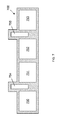
- FIG. 5 is a top view that illustrates the sheet metal cover of FIG. 2 and the gasket of FIG. 3 attached to the printed circuit board module of FIG. 1 and an underlying tray in accordance with one embodiment of the present invention.
- FIG. 6 is a cross-sectional view taken along section line A-A of FIG. 5 .
- FIG. 7 is a top view of an electrically conductive EMI gasket, which can be used to replace the gasket of FIG. 3 in accordance with an alternate embodiment of the present invention.
- FIG. 8 is a top view that illustrates sheet metal cover of FIG. 2 and the gasket of FIG. 7 attached to the printed circuit board module of FIG. 1 and an underlying tray in accordance with one embodiment of the present invention.
- Electronic devices such as ASICs, FPGAs and discrete electronic circuit elements, are mounted on the top and bottom surfaces of PCB 101 in a manner well known to those of ordinary skill.
- Electronic devices mounted on the top surface of PCB 101 are generally illustrated as squares having solid lines in FIG. 1A
- electronic devices mounted on the bottom surface of PCB 101 are illustrated as squares having dashed lines.
- FIG. 1 Although there are many electronic devices mounted on the top and bottom surfaces of PCB 101 , only top-surface mounted electronic devices 121 - 129 and bottom-surface mounted electronic devices 131 - 133 are labeled in FIG. 1 .
- heat sinks 150 - 155 are mounted on top of heat generating electronic devices (not shown in FIG. 1A ), which are mounted on the top surface of PCB 101 .
- Inductors 161 - 163 which generate significant amounts of heat during the normal operation of PCB module 100 , are also mounted on the top surface of PCB 101 .
- Printed circuit board 101 includes internal ground planes 140 , which stabilize a ground supply voltage reference to the various electronic devices mounted on PCB 101 in a manner known to those of ordinary skill in the art.
- Internal ground plane 140 is located between the upper and lower surfaces of PCB 101 (i.e., is not exposed at the upper/lower surfaces of PCB 101 ).
- Mounting hole structures 141 - 149 provide electrical connections to internal ground plane 140 in a manner described in more detail below.
- FIG. 1B is a cross sectional view of mounting hole structure 141 in accordance with one embodiment of the present invention. It is understood that mounting hole structures 142 - 149 are substantially identical to mounting hole structure 141 .
- Mounting hole structure 141 includes a mounting hole 141 A that extends through PCB 101 , electrically conductive pads 141 B that surround the mounting hole 141 A on the upper surface of PCB 101 , and electrically conductive traces 141 C that extend through PCB 101 to connect pads 141 B to internal ground plane 140 .
- mounting hole structures in addition to mounting hole structures 141 - 149 are included on PCB 101 , but are not labeled with reference numbers for reasons of clarity. In accordance with one embodiment, these additional mounting hole structures also provide electrical connections to internal ground plane 140 .
- FIG. 2 is a top view of a sheet metal cover 200 in accordance with one embodiment of the present invention.
- Sheet metal cover 200 includes a substantially planar elevated section 201 and legs 211 - 219 .
- Mounting holes 241 - 249 are formed at the bottoms of legs 211 - 229 , respectively. Openings 250 - 251 and 261 - 263 are formed through elevated section 201 as illustrated.
- mounting holes 241 - 249 are aligned with mounting hole structures 141 - 149 , respectively, and connector elements (e.g., screws/bolts) are inserted to connect sheet metal cover 200 to PCB module 100 .
- connector elements e.g., screws/bolts
- heat sinks 150 - 152 and electronic module 126 are exposed through opening 250 , and heat sinks 153 - 155 are exposed through opening 251 .
- heat sinks 150 - 155 extend through openings 250 - 251 without contacting sheet metal cover 200 .
- inductors 161 - 163 are exposed through openings 261 - 263 , respectively.
- Electronic device 127 is also exposed through opening 252 .
- FIG. 3 is a top view of an EMI gasket 300 in accordance with one embodiment of the present invention.
- Gasket 300 is constructed of a material that is electrically conductive.
- gasket 300 is constructed of conventional fabric-over-foam EMI gasketing material (e.g., rip-stop nylon fabric with conductive nickel plated strands within the weave).
- Gasket 300 may alternately be constructed of other electrically conductive material such as beryllium copper (BeCu), sheet metal, copper tape or Mylar® coated/plated with an electrically conductive material. It is understood that other electrically conductive materials can be used to implement gasket 300 in other embodiments.
- Gasket 300 is dimensioned to fit under the elevated section 201 of sheet metal cover 200 .
- Gasket 300 includes openings 328 , 350 - 352 and 361 - 363 .
- gasket 300 is attached to the underside of the elevated section 201 of sheet metal cover 200 by an electrically conductive adhesive (e.g., epoxy), such that openings 350 - 352 of gasket 300 are aligned with openings 250 - 252 of sheet metal cover 200 , respectively.
- Openings 361 - 363 of gasket 300 are also aligned with openings 261 - 263 , respectively, of sheet metal cover 200 .
- the opening 328 of gasket 300 is aligned with electronic device 128 on PCB 101 when sheet metal cover 200 is mounted on PCB 101 .
- FIG. 4 is a top view that shows gasket 300 mounted underneath the elevated section 201 of sheet metal cover 200 , in accordance with one embodiment of the present invention.
- gasket 300 is dimensioned such that portions of gasket 300 extend partially into openings 250 - 251 and 261 - 263 , as illustrated. That is, the openings 350 - 351 and 361 - 363 in gasket 300 are slightly smaller than the corresponding openings 250 - 251 and 262 - 263 in sheet metal cover 200 .
- FIG. 5 is a top view that illustrates sheet metal cover 200 and gasket 300 attached to PCB module 100 and an underlying tray 500 in accordance with one embodiment of the present invention.
- FIG. 6 is a cross-sectional view taken along section line A-A of FIG. 5 . Note that FIG. 6 illustrates the electronic device 129 upon which heat sink 154 is mounted.
- Screws 541 - 549 are inserted through the mounting holes 241 - 249 , respectively, in sheet metal cover 200 and through the mounting hole structures 141 - 149 , respectively, of PCB 101 . Screws 541 - 549 engage with corresponding posts in the underlying tray 500 . For example, as illustrated by FIG. 6 , screws 543 - 545 engage with posts 503 - 505 , respectively, of tray 500 . As a result, PCB module 100 is suspended over (and attached to) tray 500 . Screws 541 - 549 force sheet metal cover 200 into electrical contact with the electrically conductive pads of the mounting hole structures 141 - 149 of PCB 100 (e.g., pads 141 B of FIG.
- tray 500 and the associated posts are electrically conductive (e.g., metal), and are also grounded.
- screws 541 - 549 are also electrically conductive. Grounding sheet metal cover 200 in this manner advantageously reduces the radiated emissions exiting the smaller grounded cavities that are formed by the resulting assembly.
- heat sinks 150 - 152 and electronic device 126 are exposed through opening 250 of sheet metal cover 200 and opening 350 of gasket 300
- heat sinks 153 - 155 are exposed through opening 251 of sheet metal cover 200 and opening 351 of gasket 300 .
- the edges of gasket 300 that define openings 350 and 351 are placed in physical and electrical contact with associated heat sinks.
- edges of gasket 300 are placed into contact with heat sinks 150 - 154 .
- An electrically conductive adhesive can be used to attach the edges of gasket 300 to the heat sinks 150 - 154 .
- the electrically conductive gasket 300 further reduces the transmission of electromagnetic energy through the cover.
- FIG. 7 is a top view of an electrically conductive gasket 700 , which can be used to replace gasket 300 in accordance with an alternate embodiment of the present invention.
- Gasket 700 includes openings 750 - 755 , which are dimensioned and positioned to engage with each of the edges of heat sinks 150 - 155 , respectively.
- Gasket 700 is attached to the underside of sheet metal cover 200 in the manner described above, such that openings 750 - 752 are exposed through opening 250 in sheet metal cover 200 , and openings 753 - 755 are exposed through opening 251 of sheet metal cover 200 .
- FIG. 8 is a top view that illustrates sheet metal cover 200 and gasket 700 attached to PCB module 100 and underlying tray 500 in accordance with the present embodiment.
- Electrically conductive gasket 700 laterally surrounds and electrically contacts each of the edges of heat sinks 150 - 155 , thereby further reducing the transmission of electromagnetic energy through the cover structure.
- an electrically conductive adhesive can be used to connect gasket 700 to heat sinks 150 - 155 .
- gasket material is only present at locations near where the gasket 700 is placed into electrical contact with the heat sinks 150 - 155 .
- the coverage provided by gasket 700 can be extended.
- the gasket 300 of FIG. 3 can be modified by replacing the openings 350 - 351 with openings similar to the openings 750 - 755 of gasket 700 .
- inductors 161 - 163 are exposed through openings 261 - 263 , respectively, of sheet metal cover 200 and through openings 361 - 363 , respectively, of gasket 300 .
- Electronic device 127 is exposed through opening 252 of sheet metal cover 200 and opening 352 of gasket 300 .
- Electronic device 128 is exposed through opening 328 of the electrically conductive EMI gasket 300 .
- Exposing heat sinks 150 - 155 , inductors 161 - 163 and electronic devices 126 - 128 in the above-described manner advantageously facilitates the transfer of heat away from these elements. That is, airflow introduced across the resulting structure will advantageously provide direct cooling of heat sinks 150 - 155 , inductors 161 - 163 and electronic devices 126 - 128 .
- Sheet metal cover 200 and gasket 300 physically cover selected electronic devices (e.g., electronic devices 122 - 125 ) on the upper surface of PCB module 100 , thereby preventing probing/viewing of these electronic devices.
- electronic devices e.g., electronic devices 122 - 125
- sensitive signals e.g., heat sinks and inductors
- Sheet metal cover 200 is inexpensive to fabricate, using conventional sheet metal processing techniques (e.g., stamping and pressing).
- grounded sheet metal cover 200 advantageously limits electromagnetic radiation from PCB module 100 .
- the electronic devices 131 - 133 mounted on the lower surface of PCB 101 tend to emit electromagnetic signals, from the radiating component(s) on the surface of PCB 101 during normal operation of PCB module 100 .
- Grounded sheet metal cover 200 and gasket 300 significantly reduce the propagation of these electromagnetic signals, thereby reducing electromagnetic interference (EMI) with nearby devices/modules.
- EMI electromagnetic interference
Landscapes
- Engineering & Computer Science (AREA)
- Microelectronics & Electronic Packaging (AREA)
- Physics & Mathematics (AREA)
- Thermal Sciences (AREA)
- Shielding Devices Or Components To Electric Or Magnetic Fields (AREA)
Abstract
Description
Claims (12)
Priority Applications (1)
| Application Number | Priority Date | Filing Date | Title |
|---|---|---|---|
| US13/558,321 US9516795B2 (en) | 2012-01-10 | 2012-07-25 | Printed circuit board cover |
Applications Claiming Priority (2)
| Application Number | Priority Date | Filing Date | Title |
|---|---|---|---|
| US201261585210P | 2012-01-10 | 2012-01-10 | |
| US13/558,321 US9516795B2 (en) | 2012-01-10 | 2012-07-25 | Printed circuit board cover |
Publications (2)
| Publication Number | Publication Date |
|---|---|
| US20130176684A1 US20130176684A1 (en) | 2013-07-11 |
| US9516795B2 true US9516795B2 (en) | 2016-12-06 |
Family
ID=48743778
Family Applications (1)
| Application Number | Title | Priority Date | Filing Date |
|---|---|---|---|
| US13/558,321 Expired - Fee Related US9516795B2 (en) | 2012-01-10 | 2012-07-25 | Printed circuit board cover |
Country Status (1)
| Country | Link |
|---|---|
| US (1) | US9516795B2 (en) |
Cited By (2)
| Publication number | Priority date | Publication date | Assignee | Title |
|---|---|---|---|---|
| US10108234B1 (en) * | 2017-06-09 | 2018-10-23 | Nzxt Inc. | Shielded motherboard |
| US20210120666A1 (en) * | 2019-04-12 | 2021-04-22 | Skyworks Solutions, Inc. | Method for shielding a printed circuit board from electromagnetic interference and noise during testing |
Families Citing this family (7)
| Publication number | Priority date | Publication date | Assignee | Title |
|---|---|---|---|---|
| JP2017123395A (en) * | 2016-01-07 | 2017-07-13 | アルプス電気株式会社 | Electronic circuit module |
| US11029985B2 (en) | 2018-01-19 | 2021-06-08 | Ge Aviation Systems Llc | Processor virtualization in unmanned vehicles |
| US11032919B2 (en) * | 2018-01-19 | 2021-06-08 | Ge Aviation Systems Llc | Control boxes and system-on-module circuit boards for unmanned vehicles |
| US10827629B2 (en) * | 2018-01-19 | 2020-11-03 | Ge Aviation Systems Llc | Control boxes and system-on-module circuit boards for unmanned vehicles |
| US10942509B2 (en) | 2018-01-19 | 2021-03-09 | Ge Aviation Systems Llc | Heterogeneous processing in unmanned vehicles |
| CN109089376A (en) * | 2018-07-25 | 2018-12-25 | 上海斐讯数据通信技术有限公司 | Connection structure between a kind of pcb board |
| CN111182714B (en) * | 2020-01-17 | 2021-02-12 | 西安联飞智能装备研究院有限责任公司 | UAV circuit layout structure |
Citations (22)
| Publication number | Priority date | Publication date | Assignee | Title |
|---|---|---|---|---|
| US5508889A (en) * | 1994-06-29 | 1996-04-16 | Molex Incorporated | Shield cover and shielding method using the same |
| US6185099B1 (en) * | 1998-04-02 | 2001-02-06 | Steve Igenierie | Cooling device for an electronic power system |
| US6239359B1 (en) * | 1999-05-11 | 2001-05-29 | Lucent Technologies, Inc. | Circuit board RF shielding |
| US20010053070A1 (en) * | 2000-06-19 | 2001-12-20 | Keihin Corporation | Electronic unit equipped with electromagnetic shielding plate |
| US20020075664A1 (en) * | 2000-12-19 | 2002-06-20 | Perkins Russell Wayne | Method and apparatus for providing electromagnetic shielding |
| US6462436B1 (en) * | 1999-08-13 | 2002-10-08 | Avaya Technology Corp. | Economical packaging for EMI shields on PCB |
| US6501018B2 (en) * | 2001-01-31 | 2002-12-31 | Hewlett-Packard Company | EMI gasket having enhanced z-axis compliance |
| US20030107881A1 (en) * | 2001-12-11 | 2003-06-12 | Ngk Insulators, Ltd. | Setting construction of shield case or planar antenna on circuit board |
| US20030136812A1 (en) * | 2002-01-24 | 2003-07-24 | Nas Interplex, Inc. | Solder-bearing electromagnetic shield |
| US20030169583A1 (en) * | 2002-03-06 | 2003-09-11 | Alps Electric Co., Ltd. | Shielding structure suitable for use with transmitter-receivers |
| US20030193794A1 (en) * | 2002-04-10 | 2003-10-16 | Bradley Reis | Board-level EMI shield with enhanced thermal dissipation |
| US20030223213A1 (en) * | 2002-05-30 | 2003-12-04 | Daoud Bassel H. | Electromagnetic interference shield |
| US20070071886A1 (en) * | 2001-03-19 | 2007-03-29 | Babb Samuel M | Board-level EMI shield that adheres to and conforms with printed circuit board component and board surfaces |
| US20070103882A1 (en) * | 2005-11-04 | 2007-05-10 | Hon Hai Precision Industry Co., Ltd. | Electronic device with shield |
| US7262369B1 (en) * | 2006-03-09 | 2007-08-28 | Laird Technologies, Inc. | Combined board level EMI shielding and thermal management |
| US7351107B1 (en) * | 2007-01-03 | 2008-04-01 | Delphi Technologies, Inc. | One-piece electromagnetic shield having mechanical attachment features |
| US7355857B2 (en) * | 2006-02-07 | 2008-04-08 | Methode Electronics, Inc. | Heat sink gasket |
| US20080192446A1 (en) * | 2007-02-09 | 2008-08-14 | Johannes Hankofer | Protection For Circuit Boards |
| US20090184405A1 (en) * | 2008-01-23 | 2009-07-23 | Advanced Semiconductor Engineering, Inc. | Package structure |
| US7625223B1 (en) * | 2008-10-01 | 2009-12-01 | Tyco Electronics Corporation | Connector system with floating heat sink |
| US20100097771A1 (en) * | 2008-10-21 | 2010-04-22 | Chi Mei Communication Systems, Inc. | Circuit board assembly |
| US20100246143A1 (en) * | 2009-03-26 | 2010-09-30 | Richard Hung Minh Dinh | Electromagnetic Interference Shielding for Compact Electronic Devices |
-
2012
- 2012-07-25 US US13/558,321 patent/US9516795B2/en not_active Expired - Fee Related
Patent Citations (22)
| Publication number | Priority date | Publication date | Assignee | Title |
|---|---|---|---|---|
| US5508889A (en) * | 1994-06-29 | 1996-04-16 | Molex Incorporated | Shield cover and shielding method using the same |
| US6185099B1 (en) * | 1998-04-02 | 2001-02-06 | Steve Igenierie | Cooling device for an electronic power system |
| US6239359B1 (en) * | 1999-05-11 | 2001-05-29 | Lucent Technologies, Inc. | Circuit board RF shielding |
| US6462436B1 (en) * | 1999-08-13 | 2002-10-08 | Avaya Technology Corp. | Economical packaging for EMI shields on PCB |
| US20010053070A1 (en) * | 2000-06-19 | 2001-12-20 | Keihin Corporation | Electronic unit equipped with electromagnetic shielding plate |
| US20020075664A1 (en) * | 2000-12-19 | 2002-06-20 | Perkins Russell Wayne | Method and apparatus for providing electromagnetic shielding |
| US6501018B2 (en) * | 2001-01-31 | 2002-12-31 | Hewlett-Packard Company | EMI gasket having enhanced z-axis compliance |
| US20070071886A1 (en) * | 2001-03-19 | 2007-03-29 | Babb Samuel M | Board-level EMI shield that adheres to and conforms with printed circuit board component and board surfaces |
| US20030107881A1 (en) * | 2001-12-11 | 2003-06-12 | Ngk Insulators, Ltd. | Setting construction of shield case or planar antenna on circuit board |
| US20030136812A1 (en) * | 2002-01-24 | 2003-07-24 | Nas Interplex, Inc. | Solder-bearing electromagnetic shield |
| US20030169583A1 (en) * | 2002-03-06 | 2003-09-11 | Alps Electric Co., Ltd. | Shielding structure suitable for use with transmitter-receivers |
| US20030193794A1 (en) * | 2002-04-10 | 2003-10-16 | Bradley Reis | Board-level EMI shield with enhanced thermal dissipation |
| US20030223213A1 (en) * | 2002-05-30 | 2003-12-04 | Daoud Bassel H. | Electromagnetic interference shield |
| US20070103882A1 (en) * | 2005-11-04 | 2007-05-10 | Hon Hai Precision Industry Co., Ltd. | Electronic device with shield |
| US7355857B2 (en) * | 2006-02-07 | 2008-04-08 | Methode Electronics, Inc. | Heat sink gasket |
| US7262369B1 (en) * | 2006-03-09 | 2007-08-28 | Laird Technologies, Inc. | Combined board level EMI shielding and thermal management |
| US7351107B1 (en) * | 2007-01-03 | 2008-04-01 | Delphi Technologies, Inc. | One-piece electromagnetic shield having mechanical attachment features |
| US20080192446A1 (en) * | 2007-02-09 | 2008-08-14 | Johannes Hankofer | Protection For Circuit Boards |
| US20090184405A1 (en) * | 2008-01-23 | 2009-07-23 | Advanced Semiconductor Engineering, Inc. | Package structure |
| US7625223B1 (en) * | 2008-10-01 | 2009-12-01 | Tyco Electronics Corporation | Connector system with floating heat sink |
| US20100097771A1 (en) * | 2008-10-21 | 2010-04-22 | Chi Mei Communication Systems, Inc. | Circuit board assembly |
| US20100246143A1 (en) * | 2009-03-26 | 2010-09-30 | Richard Hung Minh Dinh | Electromagnetic Interference Shielding for Compact Electronic Devices |
Cited By (4)
| Publication number | Priority date | Publication date | Assignee | Title |
|---|---|---|---|---|
| US10108234B1 (en) * | 2017-06-09 | 2018-10-23 | Nzxt Inc. | Shielded motherboard |
| US20210120666A1 (en) * | 2019-04-12 | 2021-04-22 | Skyworks Solutions, Inc. | Method for shielding a printed circuit board from electromagnetic interference and noise during testing |
| US11729899B2 (en) * | 2019-04-12 | 2023-08-15 | Skyworks Solutions, Inc. | Method for shielding a printed circuit board from electromagnetic interference and noise during testing |
| US12289822B2 (en) | 2019-04-12 | 2025-04-29 | Skyworks Solutions, Inc. | Method for shielding a printed circuit board from electromagnetic interference and noise during testing |
Also Published As
| Publication number | Publication date |
|---|---|
| US20130176684A1 (en) | 2013-07-11 |
Similar Documents
| Publication | Publication Date | Title |
|---|---|---|
| US9516795B2 (en) | Printed circuit board cover | |
| EP1895826B1 (en) | Electronic Appliance with a metallic heat dissipating member | |
| US11032953B2 (en) | Mutually shielded printed circuit board assembly | |
| US6744640B2 (en) | Board-level EMI shield with enhanced thermal dissipation | |
| US9048124B2 (en) | Heat sinking and electromagnetic shielding structures | |
| US6777620B1 (en) | Circuit board | |
| US20110235278A1 (en) | Circuit module | |
| CA2394064A1 (en) | Integrated convection and conduction heat sink for multiple mounting positions | |
| US6944025B2 (en) | EMI shielding apparatus | |
| US6956285B2 (en) | EMI grounding pins for CPU/ASIC chips | |
| WO2017105616A1 (en) | Sliding thermal shield | |
| US6943436B2 (en) | EMI heatspreader/lid for integrated circuit packages | |
| US20050276027A1 (en) | Electronic device for shielding EMI | |
| US20040012939A1 (en) | EMI shielding apparatus | |
| CN107396621B (en) | Electromagnetic shield for electronic device | |
| US7145774B2 (en) | Backside cooling apparatus for modular platforms | |
| US20100309632A1 (en) | Motherboard with mounting holes | |
| KR101392668B1 (en) | Sheet-metal structure and electronic device | |
| US6707675B1 (en) | EMI containment device and method | |
| CN215991337U (en) | Circuit board heat dissipation shielding structure and electronic device | |
| JP5320801B2 (en) | Electronic device and noise shielding method thereof | |
| US6262363B1 (en) | Electromagnetic shielding method and apparatus | |
| EP4687378A1 (en) | Electronic device | |
| JP2022133484A (en) | electronic circuit module | |
| JP2003243549A (en) | Electronic equipment |
Legal Events
| Date | Code | Title | Description |
|---|---|---|---|
| AS | Assignment |
Owner name: BROCADE COMMUNICATIONS SYSTEMS, INC., CALIFORNIA Free format text: ASSIGNMENT OF ASSIGNORS INTEREST;ASSIGNORS:MOORE, ALSTON C., JR.;SIECHEN, MARK G.;REEL/FRAME:028639/0992 Effective date: 20120724 |
|
| STCF | Information on status: patent grant |
Free format text: PATENTED CASE |
|
| AS | Assignment |
Owner name: BROCADE COMMUNICATIONS SYSTEMS LLC, CALIFORNIA Free format text: CHANGE OF NAME;ASSIGNOR:BROCADE COMMUNICATIONS SYSTEMS, INC.;REEL/FRAME:044891/0536 Effective date: 20171128 |
|
| AS | Assignment |
Owner name: AVAGO TECHNOLOGIES INTERNATIONAL SALES PTE. LIMITED, SINGAPORE Free format text: ASSIGNMENT OF ASSIGNORS INTEREST;ASSIGNOR:BROCADE COMMUNICATIONS SYSTEMS LLC;REEL/FRAME:047270/0247 Effective date: 20180905 Owner name: AVAGO TECHNOLOGIES INTERNATIONAL SALES PTE. LIMITE Free format text: ASSIGNMENT OF ASSIGNORS INTEREST;ASSIGNOR:BROCADE COMMUNICATIONS SYSTEMS LLC;REEL/FRAME:047270/0247 Effective date: 20180905 |
|
| FEPP | Fee payment procedure |
Free format text: MAINTENANCE FEE REMINDER MAILED (ORIGINAL EVENT CODE: REM.); ENTITY STATUS OF PATENT OWNER: LARGE ENTITY |
|
| LAPS | Lapse for failure to pay maintenance fees |
Free format text: PATENT EXPIRED FOR FAILURE TO PAY MAINTENANCE FEES (ORIGINAL EVENT CODE: EXP.); ENTITY STATUS OF PATENT OWNER: LARGE ENTITY |
|
| STCH | Information on status: patent discontinuation |
Free format text: PATENT EXPIRED DUE TO NONPAYMENT OF MAINTENANCE FEES UNDER 37 CFR 1.362 |
|
| FP | Lapsed due to failure to pay maintenance fee |
Effective date: 20201206 |