US9514683B2 - Gate driving circuit, gate driving method, gate on array (GOA) circuit and display device - Google Patents

Gate driving circuit, gate driving method, gate on array (GOA) circuit and display device Download PDF

Info

Publication number
US9514683B2
US9514683B2 US14/415,082 US201414415082A US9514683B2 US 9514683 B2 US9514683 B2 US 9514683B2 US 201414415082 A US201414415082 A US 201414415082A US 9514683 B2 US9514683 B2 US 9514683B2
Authority
US
United States
Prior art keywords
pulling
electrode
node
potential
level
Prior art date
Legal status (The legal status is an assumption and is not a legal conclusion. Google has not performed a legal analysis and makes no representation as to the accuracy of the status listed.)
Active, expires
Application number
US14/415,082
Other versions
US20160019840A1 (en
Inventor
Kun CAO
Zhongyuan Wu
Liye DUAN
Current Assignee (The listed assignees may be inaccurate. Google has not performed a legal analysis and makes no representation or warranty as to the accuracy of the list.)
BOE Technology Group Co Ltd
Original Assignee
BOE Technology Group Co Ltd
Priority date (The priority date is an assumption and is not a legal conclusion. Google has not performed a legal analysis and makes no representation as to the accuracy of the date listed.)
Filing date
Publication date
Application filed by BOE Technology Group Co Ltd filed Critical BOE Technology Group Co Ltd
Assigned to BOE TECHNOLOGY GROUP CO., LTD. reassignment BOE TECHNOLOGY GROUP CO., LTD. ASSIGNMENT OF ASSIGNORS INTEREST (SEE DOCUMENT FOR DETAILS). Assignors: CAO, Kun, DUAN, LIYE, WU, ZHONGYUAN
Publication of US20160019840A1 publication Critical patent/US20160019840A1/en
Application granted granted Critical
Publication of US9514683B2 publication Critical patent/US9514683B2/en
Active legal-status Critical Current
Adjusted expiration legal-status Critical

Links

Images

Classifications

    • GPHYSICS
    • G09EDUCATION; CRYPTOGRAPHY; DISPLAY; ADVERTISING; SEALS
    • G09GARRANGEMENTS OR CIRCUITS FOR CONTROL OF INDICATING DEVICES USING STATIC MEANS TO PRESENT VARIABLE INFORMATION
    • G09G3/00Control arrangements or circuits, of interest only in connection with visual indicators other than cathode-ray tubes
    • G09G3/20Control arrangements or circuits, of interest only in connection with visual indicators other than cathode-ray tubes for presentation of an assembly of a number of characters, e.g. a page, by composing the assembly by combination of individual elements arranged in a matrix no fixed position being assigned to or needed to be assigned to the individual characters or partial characters
    • G09G3/22Control arrangements or circuits, of interest only in connection with visual indicators other than cathode-ray tubes for presentation of an assembly of a number of characters, e.g. a page, by composing the assembly by combination of individual elements arranged in a matrix no fixed position being assigned to or needed to be assigned to the individual characters or partial characters using controlled light sources
    • G09G3/30Control arrangements or circuits, of interest only in connection with visual indicators other than cathode-ray tubes for presentation of an assembly of a number of characters, e.g. a page, by composing the assembly by combination of individual elements arranged in a matrix no fixed position being assigned to or needed to be assigned to the individual characters or partial characters using controlled light sources using electroluminescent panels
    • G09G3/32Control arrangements or circuits, of interest only in connection with visual indicators other than cathode-ray tubes for presentation of an assembly of a number of characters, e.g. a page, by composing the assembly by combination of individual elements arranged in a matrix no fixed position being assigned to or needed to be assigned to the individual characters or partial characters using controlled light sources using electroluminescent panels semiconductive, e.g. using light-emitting diodes [LED]
    • G09G3/3208Control arrangements or circuits, of interest only in connection with visual indicators other than cathode-ray tubes for presentation of an assembly of a number of characters, e.g. a page, by composing the assembly by combination of individual elements arranged in a matrix no fixed position being assigned to or needed to be assigned to the individual characters or partial characters using controlled light sources using electroluminescent panels semiconductive, e.g. using light-emitting diodes [LED] organic, e.g. using organic light-emitting diodes [OLED]
    • G09G3/3266Details of drivers for scan electrodes
    • GPHYSICS
    • G09EDUCATION; CRYPTOGRAPHY; DISPLAY; ADVERTISING; SEALS
    • G09GARRANGEMENTS OR CIRCUITS FOR CONTROL OF INDICATING DEVICES USING STATIC MEANS TO PRESENT VARIABLE INFORMATION
    • G09G3/00Control arrangements or circuits, of interest only in connection with visual indicators other than cathode-ray tubes
    • G09G3/20Control arrangements or circuits, of interest only in connection with visual indicators other than cathode-ray tubes for presentation of an assembly of a number of characters, e.g. a page, by composing the assembly by combination of individual elements arranged in a matrix no fixed position being assigned to or needed to be assigned to the individual characters or partial characters
    • G09G3/22Control arrangements or circuits, of interest only in connection with visual indicators other than cathode-ray tubes for presentation of an assembly of a number of characters, e.g. a page, by composing the assembly by combination of individual elements arranged in a matrix no fixed position being assigned to or needed to be assigned to the individual characters or partial characters using controlled light sources
    • G09G3/30Control arrangements or circuits, of interest only in connection with visual indicators other than cathode-ray tubes for presentation of an assembly of a number of characters, e.g. a page, by composing the assembly by combination of individual elements arranged in a matrix no fixed position being assigned to or needed to be assigned to the individual characters or partial characters using controlled light sources using electroluminescent panels
    • G09G3/32Control arrangements or circuits, of interest only in connection with visual indicators other than cathode-ray tubes for presentation of an assembly of a number of characters, e.g. a page, by composing the assembly by combination of individual elements arranged in a matrix no fixed position being assigned to or needed to be assigned to the individual characters or partial characters using controlled light sources using electroluminescent panels semiconductive, e.g. using light-emitting diodes [LED]
    • G09G3/3208Control arrangements or circuits, of interest only in connection with visual indicators other than cathode-ray tubes for presentation of an assembly of a number of characters, e.g. a page, by composing the assembly by combination of individual elements arranged in a matrix no fixed position being assigned to or needed to be assigned to the individual characters or partial characters using controlled light sources using electroluminescent panels semiconductive, e.g. using light-emitting diodes [LED] organic, e.g. using organic light-emitting diodes [OLED]
    • G09G3/3225Control arrangements or circuits, of interest only in connection with visual indicators other than cathode-ray tubes for presentation of an assembly of a number of characters, e.g. a page, by composing the assembly by combination of individual elements arranged in a matrix no fixed position being assigned to or needed to be assigned to the individual characters or partial characters using controlled light sources using electroluminescent panels semiconductive, e.g. using light-emitting diodes [LED] organic, e.g. using organic light-emitting diodes [OLED] using an active matrix
    • G09G3/3233Control arrangements or circuits, of interest only in connection with visual indicators other than cathode-ray tubes for presentation of an assembly of a number of characters, e.g. a page, by composing the assembly by combination of individual elements arranged in a matrix no fixed position being assigned to or needed to be assigned to the individual characters or partial characters using controlled light sources using electroluminescent panels semiconductive, e.g. using light-emitting diodes [LED] organic, e.g. using organic light-emitting diodes [OLED] using an active matrix with pixel circuitry controlling the current through the light-emitting element
    • GPHYSICS
    • G09EDUCATION; CRYPTOGRAPHY; DISPLAY; ADVERTISING; SEALS
    • G09GARRANGEMENTS OR CIRCUITS FOR CONTROL OF INDICATING DEVICES USING STATIC MEANS TO PRESENT VARIABLE INFORMATION
    • G09G2300/00Aspects of the constitution of display devices
    • G09G2300/04Structural and physical details of display devices
    • G09G2300/0404Matrix technologies
    • G09G2300/0408Integration of the drivers onto the display substrate
    • GPHYSICS
    • G09EDUCATION; CRYPTOGRAPHY; DISPLAY; ADVERTISING; SEALS
    • G09GARRANGEMENTS OR CIRCUITS FOR CONTROL OF INDICATING DEVICES USING STATIC MEANS TO PRESENT VARIABLE INFORMATION
    • G09G2300/00Aspects of the constitution of display devices
    • G09G2300/08Active matrix structure, i.e. with use of active elements, inclusive of non-linear two terminal elements, in the pixels together with light emitting or modulating elements
    • G09G2300/0809Several active elements per pixel in active matrix panels
    • G09G2300/0819Several active elements per pixel in active matrix panels used for counteracting undesired variations, e.g. feedback or autozeroing
    • GPHYSICS
    • G09EDUCATION; CRYPTOGRAPHY; DISPLAY; ADVERTISING; SEALS
    • G09GARRANGEMENTS OR CIRCUITS FOR CONTROL OF INDICATING DEVICES USING STATIC MEANS TO PRESENT VARIABLE INFORMATION
    • G09G2300/00Aspects of the constitution of display devices
    • G09G2300/08Active matrix structure, i.e. with use of active elements, inclusive of non-linear two terminal elements, in the pixels together with light emitting or modulating elements
    • G09G2300/0809Several active elements per pixel in active matrix panels
    • G09G2300/0842Several active elements per pixel in active matrix panels forming a memory circuit, e.g. a dynamic memory with one capacitor
    • G09G2300/0861Several active elements per pixel in active matrix panels forming a memory circuit, e.g. a dynamic memory with one capacitor with additional control of the display period without amending the charge stored in a pixel memory, e.g. by means of additional select electrodes
    • G09G2300/0866Several active elements per pixel in active matrix panels forming a memory circuit, e.g. a dynamic memory with one capacitor with additional control of the display period without amending the charge stored in a pixel memory, e.g. by means of additional select electrodes by means of changes in the pixel supply voltage
    • GPHYSICS
    • G09EDUCATION; CRYPTOGRAPHY; DISPLAY; ADVERTISING; SEALS
    • G09GARRANGEMENTS OR CIRCUITS FOR CONTROL OF INDICATING DEVICES USING STATIC MEANS TO PRESENT VARIABLE INFORMATION
    • G09G2300/00Aspects of the constitution of display devices
    • G09G2300/08Active matrix structure, i.e. with use of active elements, inclusive of non-linear two terminal elements, in the pixels together with light emitting or modulating elements
    • G09G2300/0809Several active elements per pixel in active matrix panels
    • G09G2300/0871Several active elements per pixel in active matrix panels with level shifting
    • GPHYSICS
    • G09EDUCATION; CRYPTOGRAPHY; DISPLAY; ADVERTISING; SEALS
    • G09GARRANGEMENTS OR CIRCUITS FOR CONTROL OF INDICATING DEVICES USING STATIC MEANS TO PRESENT VARIABLE INFORMATION
    • G09G2310/00Command of the display device
    • G09G2310/02Addressing, scanning or driving the display screen or processing steps related thereto
    • G09G2310/0264Details of driving circuits
    • G09G2310/0286Details of a shift registers arranged for use in a driving circuit
    • GPHYSICS
    • G09EDUCATION; CRYPTOGRAPHY; DISPLAY; ADVERTISING; SEALS
    • G09GARRANGEMENTS OR CIRCUITS FOR CONTROL OF INDICATING DEVICES USING STATIC MEANS TO PRESENT VARIABLE INFORMATION
    • G09G2320/00Control of display operating conditions
    • G09G2320/02Improving the quality of display appearance
    • G09G2320/0233Improving the luminance or brightness uniformity across the screen
    • GPHYSICS
    • G09EDUCATION; CRYPTOGRAPHY; DISPLAY; ADVERTISING; SEALS
    • G09GARRANGEMENTS OR CIRCUITS FOR CONTROL OF INDICATING DEVICES USING STATIC MEANS TO PRESENT VARIABLE INFORMATION
    • G09G2320/00Control of display operating conditions
    • G09G2320/04Maintaining the quality of display appearance
    • G09G2320/043Preventing or counteracting the effects of ageing
    • G09G2320/045Compensation of drifts in the characteristics of light emitting or modulating elements

Definitions

  • the present disclosure relates to the field of display technology, in particular to a gate driving circuit, a gate driving method, a gate on array (GOA) circuit and a display device.
  • a gate driving circuit a gate driving method, a gate on array (GOA) circuit and a display device.
  • GOA gate on array
  • gate on may wherein gate driving circuits are directly formed on an array substrate
  • Vth threshold voltage
  • OLED organic light-emitting electrode
  • Vth non-uniformity inside an entire OLED display panel and a Vth shift generated after a long-term operation will decrease display uniformity of the OLED display panel.
  • using an integrated gate driving technology is a development trend of the future.
  • a Vth compensation pixel design of an OLED needs peripheral driving circuits to cooperate with it, therefore higher requirements are needed for the GOA.
  • An object of the present disclosure is to provide a gate driving circuit, a gate driving method, a GOA circuit and a display device, to compensate for pixel threshold voltages and drive pixels simultaneously, thereby improving the degree of integration.
  • the present disclosure provides a gate driving circuit, connected to a row pixel unit which includes a row pixel driving module and a light emitting element connected to each other, the row pixel driving module including a driving transistor, a driving module and a compensation module, the compensation module being connected with a gate scanning signal and the driving module being connected with a driving level;
  • the gate driving circuit includes a row pixel control unit, which is configured to provide the gate scanning signal to the compensation module and provide the driving level to the driving module, so as to control the compensation module to compensate for a threshold voltage of the driving transistor and control the driving module to drive the light emitting element.
  • the row pixel control unit may include a start signal input end, a first control clock input end, a second control clock input end, a reset signal input end, an input clock end, a carry signal output end, a cutting-off control signal output end, an output level end, an output level pulling-down control end and a gate scanning signal output end;
  • the row pixel control unit may further include:
  • a pulling-up node potential pulling-up module configured to pull a potential of a pulling-up node up to a high level, when a first control clock signal and a start signal are of a high level;
  • a pulling-up node potential pulling-down module configured to pull the potential of the pulling-up node down to a first low level, when a potential of a first pulling-down node or a potential of a second pulling-down node is of a high level;
  • a first control clock switch configured to set up a connection between the first control clock input end and the first pulling-down node when the first control clock signal is of a high level
  • a second control clock switch configured to set up a connection between the second control clock input end and the second pulling-down node when a second control clock signal is of a high level
  • a first pulling-down node potential pulling-down module configured to pull the potential of the first pulling-down node down to the first low level, when the potential of the pulling-up node or the potential of the second pulling-down node is of a high level;
  • a second pulling-down node potential pulling-down module connected to the reset signal input end, configured to pull the potential of the second pulling-down node down to the first low level, when the potential of the pulling-up node or the potential of the first pulling-down node is of a high level;
  • a carry control module configured to set up a connection between the carry signal output end and the second control clock input end, when the potential of the pulling-up node is of a high level
  • a carry signal pulling-down module configured to pull a potential of the carry signal down to the first low level, when the potential of the first pulling-down node or the potential of the second pulling-down node is of a high level
  • a cutting-off control module configured to set up a connection between the second control clock input end and the cutting-off control signal output end when the potential of the pulling-up node is of a high level; and set up a connection between the cutting-off control signal output end and the second low level output end when the potential of the first pulling-down node or the potential of the second pulling-down node is of a high level;
  • a feedback module configured to transmit a cutting-off control signal to the pulling-up node potential pulling-up module and the pulling-up node potential pulling-down module, when the carry signal is of a high level
  • a gate scanning signal control module configured to set up a connection between the second control clock input end and the gate scanning signal output end, when the potential of the pulling-up node is of a high level
  • an input clock switch configured to set up a connection between the input clock end and the output level pulling-down control end, when the potential of the pulling-up node is of a high level
  • a gate scanning signal pulling-down module configured to pull a potential of the gate scanning signal down to a second low level, when the potential of the first pulling-down node or the potential of the second pulling-down node is of a high level
  • an output level pulling-down control module configured to pull a potential of the output level pulling-down control end down to the second low level, when the potential of the first pulling-down node or the potential of the second pulling-down node is of a high level
  • an output level pulling-up module configured to pull the output level up to a high level, when an output level pulling-down control end outputs the second low level
  • an output level pulling-down module configured to pull the output level down to the second low level, when the output level pulling-down control end outputs a high level.
  • the pulling-up node potential pulling-up module may include:
  • a first pulling-up node potential pulling-up transistor a gate electrode and a first electrode of which are connected to the start signal input end, and a second electrode of which is connected to the feedback module;
  • a second pulling-up node potential pulling-up transistor a gate electrode of which is connected to the first control clock input end, a first electrode of which is connected to the second electrode of the first puffing-up node potential pulling-up transistor, and a second electrode of which is connected to the pulling-up node;
  • the pulling-up node potential pulling-down module may include:
  • a first pulling-up node potential pulling-down transistor a gate electrode of which is connected to the first pulling-down node, a first electrode of which is connected to the pulling-up node, and a second electrode of which is connected to the feedback module;
  • a second pulling-up node potential pulling-down transistor a gate electrode of which is connected to the first pulling-down node, a first electrode of which is connected to the second electrode of the first pulling-up node potential pulling-down transistor, and a second electrode of which is connected with the first low level;
  • a third pulling-up node potential pulling-down transistor a gate electrode of which is connected to the second pulling-down node, a first electrode of which is connected to the pulling-up node, and a second electrode of which is connected to the feedback module;
  • a fourth pulling-up node potential pulling-down transistor a gate electrode of which is connected to the second pulling-down node, a first electrode of which is connected to the second electrode of the third pulling-up node potential pulling-down transistor, and a second electrode of which is connected with the first low level;
  • the first pulling-down node potential pulling-down module may include:
  • a first pulling-down transistor a gate electrode of which is connected to the pulling-up node, a first electrode of which is connected to the first pulling-down node, and a second electrode of which is connected to the reset signal input end;
  • a second pulling-down transistor a gate electrode of which is connected to the pulling-up node, a first electrode of which is connected to the second electrode of the first pulling-down transistor, and a second electrode of which is being connected with the first low level;
  • a third pulling-down transistor a gate electrode of which is connected to the second pulling-down node, a first electrode of which is connected to the first pulling-down node, and a second electrode of which is connected with the first low level;
  • the second pulling-down node potential pulling-down module may include:
  • a fourth pulling-down transistor a gate electrode of which is connected to the pulling-up node, a first electrode of which is connected to the second pulling-down node, and a second electrode of which is connected to the reset signal input end;
  • a fifth pulling-down transistor a gate electrode of which is connected to the pulling-up node, a first electrode of which is connected to the second electrode of the fourth pulling-down transistor, and a second electrode of which is connected with the first low level;
  • a sixth pulling-down transistor a gate electrode of which is connected to the first pulling-down node, a first electrode of which is connected to the second pulling-down node, and a second electrode of which is connected with the first low level.
  • the carry control module may include:
  • a carry control transistor a gate electrode of which is connected to the pulling-up node, a first electrode of which is connected to the second control clock input end, and a second end of which is connected to the carry signal output end;
  • the carry signal pulling-down module may include:
  • a first carry signal pulling-down transistor a gate electrode of which is connected to the first pulling-down node, a first electrode of which is connected to the carry signal output end, and a second electrode of which is connected with the first low level
  • a second carry signal pulling-down transistor a gate electrode of which is connected to the second pulling-down node, a first electrode of which is connected to the carry signal output end, and a second electrode of which is connected with the first low level
  • the cutting-off control module may include:
  • a second cutting-off control transistor a gate electrode of which is connected to the first pulling-down node, a first electrode of which is connected to the cutting-off control signal output end, and a second electrode of which is connected with the second low level
  • a third cutting-off control transistor a gate electrode of which is connected to the second pulling-down node, a first electrode of which is connected to the cutting-off control signal output end, and a second electrode of which is connected with the second low level
  • the feedback module may include:
  • a feedback transistor a gate electrode of which is connected to the carry signal output end, a first electrode of which is connected to the second electrode of the first pulling-up node potential pulling-up transistor, and a second electrode of which is connected to the cutting-off control signal output end.
  • the gate scanning signal control module may include:
  • a gate scanning control transistor a gate electrode of which is connected to the pulling-up node, a first electrode of which is connected with the second control clock signal, and a second electrode of which is connected to the gate scanning signal output end;
  • the gate scanning signal pulling-down module may include:
  • a first output pulling-down transistor a gate electrode of which is connected to the first pulling-down node, a first electrode of which is connected to the gate scanning signal output end, and a second electrode of which is connected with the second low level;
  • a second output pulling-down transistor a gate electrode of which is connected to the second pulling-down node, a first electrode of which is connected to the gate scanning signal output end, and a second electrode of which is connected with the second low level;
  • the output level pulling-up module may include:
  • an output level pulling-up transistor a gate electrode and first electrode of which are connected with a high level, and a second electrode of which is connected to the output level end;
  • the output level pulling-down control module may include:
  • a first pulling-down control transistor a gate electrode of which is connected to the first pulling-down node, a first electrode of which is connected to the output level pulling-down control end, and a second electrode of which is connected with the second low level;
  • a second pulling-down control transistor a gate electrode of which is connected to the second pulling-down node, a first electrode of which is connected to the output level pulling-down control end, and a second electrode of which is connected with the second low level;
  • the output level pulling-down module may include:
  • an output level pulling-down transistor a gate electrode of which is connected to the output level pulling-down control end, a first electrode of which is connected to the output level end, and a second electrode of which is connected with the second low level.
  • the input clock switch may include an input transistor, a gate electrode of which is connected to the pulling-up node, a first electrode of which is connected to the input clock end, and a second electrode of which is connected to output level pulling-down control end.
  • the first control clock signal and the second control clock signal may be inverted.
  • the present disclosure further provides a gate driving method, applied in the above gate driving circuit, the method including:
  • the present disclosure further provides a Gate on array (GOA) circuit, including the above multi-level gate driving circuits;
  • GAA Gate on array
  • each level gate driving circuit further includes a driving control signal output end
  • start signal input end of a first level gate driving circuit and the start signal input end of a second level gate driving circuit are inputted with the start signal;
  • N-th level gate driving circuit is connected to the carry signal output end of an (N ⁇ 2)-th level gate driving circuit, where N is an integer greater than or equal to 3 and less than or equal to M, and M is a number of levels of the gate driving circuits included in the GOA circuit;
  • each level gate driving circuit is connected to the output level end of a next level gate driving circuit;
  • the reset signal input end of a K-th level gate driving circuit is connected to the cutting-off control signal output end of a (K+2)-th level gate driving circuit, where K is an integer greater than or equal to 1 and less than M ⁇ 1;
  • the first control signal input ends of odd-number-level gate driving circuits are connected with a first external control signal
  • the second control signal input ends of the odd-number-level gate driving circuits are connected with a second external control signal
  • the first control signal input ends of even-number-level gate driving circuits are connected with a third external control signal
  • the second control signal input ends of odd-number-level gate driving circuits are connected with a fourth external control signal.
  • first control signal and the second control signal may be inverted
  • the third control signal and the fourth control signal may be inverted.
  • the third external control signal may be of one clock cycle later than the first external control signal
  • the fourth external control signal may be of one clock cycle later than the second external control signal.
  • the input clock signal inputted to a 2n-th level gate driving circuit and the input clock signal inputted to a (2n+2)-th level gate driving circuit may be inverted;
  • the input clock signal inputted to a (2n ⁇ 1)-th level gate driving circuit and the input clock signal inputted to a (2n+1)-th level gate driving circuit may be inverted;
  • the input clock signal inputted to the 2n-th level gate driving circuit may be of one clock cycle later than the input clock signal inputted to the (2n ⁇ 1)-th level gate driving circuit;
  • the input clock signal inputted to the (2n+2)-th level gate driving circuit may be of one clock cycle later than the input clock signal inputted to the (2n+1)-th level gate driving circuit;
  • n is an integer greater than or equal to 1, and 2n+2 is less than or equal to M.
  • the present disclosure further provides a display device, including the above gate driving circuit.
  • the display device may be an organic light-emitting diode (OLED) display device or a low-temperature polysilicon (LTPS) display device.
  • OLED organic light-emitting diode
  • LTPS low-temperature polysilicon
  • the gate driving circuit, the gate driving method, the GOA circuit and the display device are configured to control the compensation module to compensate for a threshold voltage of the driving transistor and control the driving module to drive the row pixel control unit of the light emitting element, which can compensate for pixel threshold voltages and drive pixels simultaneously.
  • Applying the gate driving circuit and the GOA circuit according to the present disclosure in the OLED display panel can improve the process integration of the OLED display panel and reduce costs.
  • the output level of a next level gate driving circuit and the switch signal of an immediately previous level gate driving circuit use a same signal, which can simplify the circuit.
  • FIG. 1A is a circuit diagram showing a example of a row pixel driving module included in a row pixel unit connected to a gate driving circuit according to the present disclosure
  • FIG. 1B is a diagram showing timing sequences of the row pixel driving module shown in FIG. 1A ;
  • FIG. 1C is a block diagram showing a structure of the gate driving circuit according to an embodiment of the present disclosure
  • FIG. 2 is a circuit diagram showing a gate driving circuit according to an embodiment of the present disclosure
  • FIG. 3 is a diagram showing a structure of a GOA circuit according to an embodiment of the present disclosure
  • FIG. 4A is a diagram showing timing sequences of GO_ELVDD (n), GO_S 1 (n) and GO_S 2 (n) outputted by an N-th row pixel driving module and DATA inputted to the N-th row pixel driving module;
  • FIG. 4B is a diagram showing timing sequences of GO_ELVDD (n+1), GO_S 1 (n+1) and GO_S 2 (n+1) outputted by an (N+1)-th row pixel driving module and DATA inputted to the (N+1)-th row pixel driving module;
  • FIG. 5A is a diagram showing waveforms of STV 1 , STV 2 , CLK 1 , CLK 2 , CLK 3 , CLK 4 , CLKIN 1 , CLKIN 2 , CLKIN 3 and CLKIN 4 when GOA circuit is working according to an embodiment of the present disclosure;
  • FIG. 5B is a diagram showing waveforms of GO_S 1 (n), GO_S 1 (n+1), GO_S 1 (n+2), GO_S 1 (n+3), GO_ELVDD (n), GO — ELVDD (n+1), GO — ELVDD (n+2) and GO — ELVDD (n+3) outputted by a GOA circuit according to an embodiment of the present disclosure.
  • the present disclosure provides a gate driving circuit, connected to a row pixel unit which includes a row pixel driving module and a light emitting element connected to each other, the row pixel driving module including a driving transistor, a driving module and a compensation module, the compensation module being connected with a gate scanning signal and the driving module being connected with a driving level;
  • the gate driving circuit includes a row pixel control unit, which is configured to provide the gate scanning signal to the compensation module and provide the driving level to the driving module, so as to control the compensation module to compensate for a threshold voltage of the driving transistor and control the driving module to drive the light emitting element.
  • the gate driving circuit is configured to control the compensation module to compensate for a threshold voltage of the driving transistor and control the driving module to drive the row pixel control unit of the light emitting element, which can compensate for pixel threshold voltages.
  • Applying the gate driving circuit according to the present disclosure in the OLED display panel can improve the process integration of the OLED display panel and reduce costs.
  • the row pixel driving module includes a driving transistor T 1 , a compensation transistor T 2 , a driving control transistor T 3 , a first capacitor C 1 and a second capacitor C 2 ;
  • the compensation transistor T 2 includes a compensation module
  • the driving control transistor T 3 includes a driving control module
  • a gate electrode of the compensation transistor T 2 is connected with a gate scanning signal S 1 , a second electrode of the compensation transistor T 2 is connected with a data signal DATA; a gate electrode of the driving control transistor T 3 is connected with a driving control signal S 2 , a first electrode of the driving control transistor T 3 is connected with an output level ELVDD;
  • a cathode of the OLED is connected with a voltage level ELVSS.
  • FIG. 1B is a diagram showing timing sequences of the row pixel driving module shown in FIG. 1A .
  • the present disclosure provides a GOA unit which can cooperate with the Vth compensation pixel design.
  • the GOA unit can output two signals, one output signal is a high level signal of a pulse which can be a gate scanning signal (S 1 as shown in FIG. 1A ), the other output signal is a low level signal of the pulse which can be an ELVDD (as shown in FIG. 1A ).
  • a gate scanning signal S 1 as shown in FIG. 1A
  • ELVDD as shown in FIG. 1A
  • a low level pulse signal S 2 which functions as a switch of ELVDD signal to drive the pixel.
  • the low level pulse signal S 2 can be used as the driving control signal.
  • the low level pulse signal S 2 of an N-th row and the ELVDD signal of an (N+1)-th row can use a same signal, which can simplify the circuit.
  • the pixel threshold compensation and the pixel driving can be achieved by adjusting the timing sequences of a start signal and a clock signal.
  • the row pixel control unit includes a start signal input end STV, a first control clock input end CLKA, a second control clock input end CLKB, a reset signal input end RESET, an input clock end CLKIN (n), a carry signal output end COUT (n), a cutting-off control signal output end IOFF (n), an output level end GO_ELVDD (n), an output level pulling-down control end G_VDD and a gate scanning signal output end GO_S 1 (n);
  • the row pixel control unit further includes:
  • a pulling-up node potential pulling-up module 101 configured to pull a potential of a pulling-up node up to a high level, when a first control clock signal and a start signal are of a high level;
  • a pulling-up node potential pulling-down module 102 configured to pull the potential of the pulling-up node Q down to a first low level VGL 1 , when a potential of a first pulling-down node QB 1 or a potential of a second pulling-down node QB 2 is of a high level;
  • a first control clock switch 141 configured to set up a connection between the first control clock input end CLKA and the first pulling-down node QB 1 , when the first control clock signal is of a high level;
  • a second control clock switch 142 configured to set up a connection between the second control clock input end CLKB and the second pulling-down node QB 2 , when a second control clock signal is of a high level;
  • a first pulling-down node potential pulling-down module 12 configured to pull the potential of the first pulling-down node QB 1 down to the first low level VGL 1 , when the potential of the pulling-up node Q or the potential of the second pulling-down node QB 2 is of a high level;
  • a second pulling-down node potential pulling-down module 13 connected to the reset signal input end RESET, configured to pull the potential of the second pulling-down node QB 2 down to the first low level VGL 1 , when the potential of the pulling-up node Q or the potential of the first pulling-down node QB 1 is of a high level;
  • a carry control module 151 configured to set up a connection between the carry signal output end COUT (n) and the second control clock input end CLKB, when the potential of the pulling-up node Q is of a high level;
  • a carry signal pulling-down module 152 configured to pull a potential of the carry signal down to the first low level VGL 1 , when the potential of the first pulling-down node QB 1 or the potential of the second pulling-down node QB 2 is of a high level;
  • a cutting-off control module 161 configured to set up a connection between the second control clock input end CLKB and the cutting-off control signal output end IOFF (n), when the potential of the pulling-up node Q is of a high level; and set up a connection between the cutting-off control signal output end IOFF (n) and the second low level output end VGL 2 , when the potential of the first pulling-down node QB 1 or the potential of the second pulling-down node QB 2 is of a high level;
  • a feedback module 162 configured to transmit a cutting-off control signal to the pulling-up node potential pulling-up module 101 and the pulling-up node potential pulling-down module 102 , when the carry signal is of a high level;
  • a gate scanning signal control module 171 configured to set up a connection between the second control clock input end CLKB and the gate scanning signal output end GO_S 1 (n), when the potential of the pulling-up node Q is of a high level;
  • an input clock switch 181 configured to set up a connection between the input clock end CLKIN (n) and the output level pulling-down control end G_VDD, when the potential of the pulling-up node Q is of a high level;
  • a gate scanning signal pulling-down module 172 configured to pull a potential of the gate scanning signal down to a second low level VGL 2 , when the potential of the first pulling-down node QB 1 or the potential of the second pulling-down node QB 2 is of a high level;
  • an output level pulling-up module 182 configured to pull the output level up to a high level, when an output level pulling-down control end G_VDD outputs the second low level VGL 2 ;
  • an output level pulling-down control module 183 configured to pull a potential of the output level pulling-down control end G_VDD down to the second low level VGL 2 , when the potential of the first pulling-down node QB 1 or the potential of the second pulling-down node QB 2 is of a high level;
  • an output level pulling-down module 184 configured to pull the output level down to the second low level VGL 2 , when the output level pulling-down control end G_VDD outputs a high level.
  • the gate driving circuit uses two pulling-down nodes, i.e., the first pulling-down node QB 1 and the second pulling-down node QB 2 , to pull down the output level.
  • the first pulling-down node QB 1 and the second pulling-down node QB 2 are both alternating currents (AC) in the condition of not outputting and are inverted. Therefore, the threshold shift can be reduced, and there is no gap in the pulling-down of outputs, which can improve stability and reliability.
  • the pixel threshold compensation and the pixel driving can be achieved by adjusting the start signal, the first control clock signal, the second control clock signal and the input clock signal.
  • All the transistors employed in the present disclosure can be thin film transistors (TFTs) or field effect transistors (FETs) or other devices with same characteristics.
  • TFTs thin film transistors
  • FETs field effect transistors
  • transistors in order to distinguish two electrodes other than a gate electrode of a transistor, one is called as a source electrode, and the other is called as a drain electrode.
  • transistors can be divided into N-type transistors or P-type transistors.
  • the specific use of N-type transistors or P-type transistors can be made by a person skilled in the art without creative work, which therefore will fall within the scope of the present disclosure.
  • a first electrode of a N-type transistor may be a source electrode, and a second electrode of the N-type transistor may be a drain electrode; a first electrode of a P-type transistor may be a drain electrode, and a second electrode of the P-type transistor may be a source electrode.
  • the pulling-up node potential pulling-up module 101 includes:
  • a first pulling-up node potential pulling-up transistor T 101 a gate electrode and a first electrode of which are connected to the start signal input end STV, and a second electrode of which is connected to the feedback module 162 ;
  • a second pulling-up node potential pulling-up transistor T 102 a gate electrode of which is connected to the first control clock input end CLKA, a first electrode of which is connected to the second electrode of the first pulling-up node potential pulling-up transistor T 101 , and a second electrode of which is connected to the pulling-up node Q;
  • the pulling-up node potential pulling-down module 102 includes:
  • a first pulling-up node potential pulling-down transistor T 201 a gate electrode of which is connected to the first pulling-down node QB 1 , a first electrode of which is connected to the pulling-up node Q, and a second electrode of which is connected to the feedback module 162 ;
  • a second pulling-up node potential pulling-down transistor T 202 a gate electrode of which is connected to the first pulling-down node QB 1 , a first electrode of which is connected to the second electrode of the first pulling-up node potential pulling-down transistor T 201 , and a second electrode of which is connected with the first low level VGL 1 ;
  • a third pulling-up node potential pulling-down transistor T 203 a gate electrode of which is connected to the second pulling-down node QB 2 , a first electrode of which is connected to the pulling-up node Q, and a second electrode of which is connected to the feedback module 162 ;
  • a fourth pulling-up node potential pulling-down transistor T 204 a gate electrode of which is connected to the second pulling-down node QB 2 , a first electrode of which is connected to the second electrode of the third pulling-up node potential pulling-down transistor T 203 , and a second electrode of which is connected with the first low level VGL 1 ;
  • the first pulling-down node potential pulling-down module 12 includes:
  • a first pulling-down transistor T 21 a gate electrode of which is connected to the pulling-up node Q, a first electrode of which is connected to the first pulling-down node QB 1 , and a second electrode of which is connected to the reset signal input end RESET;
  • a second pulling-down transistor T 22 a gate electrode of which is connected to the pulling-up node Q, a first electrode of which is connected to the second electrode of the first pulling-down transistor T 21 , and a second electrode of which is being connected with the first low level VGL 1 ;
  • a third pulling-down transistor T 23 a gate electrode of which is connected to the second pulling-down node QB 2 , a first electrode of which is connected to the first pulling-down node QB 1 , and a second electrode of which is connected with the first low level VGL 1 ;
  • the second pulling-down node potential pulling-down module 13 includes:
  • a fourth pulling-down transistor T 31 a gate electrode of which is connected to the pulling-up node Q, a first electrode of which is connected to the second pulling-down node QB 2 , and a second electrode of which is connected to the reset signal input end RESET;
  • a fifth pulling-down transistor T 32 a gate electrode of which is connected to the pulling-up node Q, a first electrode of which is connected to the second electrode of the third pulling-down transistor T 31 , and a second electrode of which is connected with the first low level VGL 1 ;
  • a sixth pulling-down transistor T 33 a gate electrode of which is connected to the first pulling-down node QB 1 , a first electrode of which is connected to the second pulling-down node QB 2 , and a second electrode of which is connected with the first low level VGL 1 .
  • the carry control module 151 includes:
  • a carry control transistor T 51 a gate electrode of which is connected to the pulling-up node Q, a first electrode of which is connected to the second control clock input end CLKB, and a second end of which is connected to the carry signal output end COUT (n);
  • the carry signal pulling-down module 152 includes:
  • a first carry signal pulling-down transistor T 521 a gate electrode of which is connected to the first pulling-down node QB 1 , a first electrode of which is connected to the carry signal output end COUT (n), and a second electrode of which is connected with the first low level VGL 1 ;
  • a second carry signal pulling-down transistor T 522 a gate electrode of which is connected to the second pulling-down node QB 2 , a first electrode of which is connected to the carry signal output end COUT (n), and a second electrode of which is connected with the first low level VGL 1 ;
  • the cutting-off control module 161 includes:
  • a first cutting-off control transistor T 611 a gate electrode of which is connected to the pulling-up node Q, a first electrode of which is connected to the second control clock input end CLKB, and a second electrode of which is connected to the cutting-off control signal output end IOFF (n);
  • a second cutting-off control transistor T 612 a gate electrode of which is connected to the first pulling-down node QB 1 , a first electrode of which is connected to the cutting-off control signal output end IOFF (n), and a second electrode of which is connected with the second low level VGL 2 ;
  • a third cutting-off control transistor T 613 a gate electrode of which is connected to the second pulling-down node QB 2 , a first electrode of which is connected to the cutting-off control signal output end IOFF (n), and a second electrode of which is connected with the second low level VGL 2 ;
  • the feedback module 162 includes:
  • a feedback transistor T 62 a gate electrode of which is connected to the carry signal output end COUT (n), a first electrode of which is connected to the second electrode of the first pulling-up node potential pulling-up transistor T 101 , and a second electrode of which is connected to the cutting-off control signal output end IOFF (n).
  • the gate scanning signal control module 171 includes:
  • a gate scanning control transistor T 71 a gate electrode of which is connected to the pulling-up node Q, a first electrode of which is connected with the second control clock signal CLKB, and a second electrode of which is connected to the gate scanning signal output end GO_S 1 (n);
  • the gate scanning signal pulling-down module 172 includes:
  • a first output pulling-down transistor T 721 a gate electrode of which is connected to the first pulling-down node QB 1 , a first electrode of which is connected to the gate scanning signal output end GO_S 1 (n), and a second electrode of which is connected with the second low level VGL 2 ;
  • a second output pulling-down transistor T 722 a gate electrode of which is connected to the second pulling-down node QB 2 , a first electrode of which is connected to the gate scanning signal output end GO_S 1 (n), and a second electrode of which is connected with the second low level VGL 2 ;
  • the input clock switch 181 includes:
  • an input transistor T 81 a gate electrode of which is connected to the pulling-up node Q, a first electrode of which is connected to an input clock end CLKIN, a second electrode of which is connected to the output level pulling-down control end G_VDD;
  • the output level pulling-up module 182 includes:
  • an output level pulling-up transistor T 82 a gate electrode and first electrode of which are connected with a high level VDD, and a second electrode of which is connected to the output level end GO_ELVDD (n);
  • the output level pulling-down control module 183 includes:
  • a first pulling-down control transistor T 831 a gate electrode of which is connected to the first pulling-down node QB 1 , a first electrode of which is connected to the output level pulling-down control end G_VDD, and a second electrode of which is connected with the second low level VGL 2 ;
  • a second pulling-down control transistor T 832 a gate electrode of which is connected to the second pulling-down node QB 2 , a first electrode of which is connected to the output level pulling-down control end G_VDD, and a second electrode of which is connected with the second low level VGL 2 ;
  • the output level pulling-down module 184 includes:
  • an output level pulling-down transistor T 84 a gate electrode of which is connected to the output level pulling-down control end G_VDD, a first electrode of which is connected to the output level end GO_ELVDD (n), and a second electrode of which is connected with the second low level VGL 2 .
  • the first control clock signal and second control clock signal may be inverted.
  • the first control clock switch 141 includes:
  • a first control transistor T 41 a gate electrode and a first electrode of which are connected to the first control clock input end CLKA, and a second electrode of which is connected to the first pulling-down node QB 1 .
  • the second control clock switch 142 includes:
  • a second control transistor T 42 a gate electrode and a first electrode of which are connected to the second control clock input end CLKB, and a second electrode of which is connected to the second pulling-down node QB 2 .
  • the storage capacitor C is connected between the pulling-up node Q and the carry signal output end COUT (n).
  • T 101 , T 102 , T 42 , T 201 , T 202 , T 203 and T 204 are P-type transistors
  • T 21 , T 22 , T 31 , T 32 , T 41 , T 51 , T 521 , T 522 , T 611 , T 612 , T 613 , T 62 , T 71 , T 721 , T 722 , T 81 , T 82 , T 831 , T 832 and T 84 are N-type transistors.
  • the type of the transistors can be changed as long as they can achieve the same effect of controlling the connection and disconnection.
  • An embodiment of the present disclosure further provides a gate driving method, applied in the above gate driving circuits, including:
  • An embodiment of the present disclosure further provides a GOA circuit, including multi-level gate driving circuits described above;
  • each level gate driving circuit further includes a driving control signal output end
  • start signal input end of a first level gate driving circuit and the start signal input end of a second level gate driving circuit are inputted with the start signal;
  • N-th level gate driving circuit is connected to the carry signal output end of an (N ⁇ 2)-th level gate driving circuit, where N is an integer greater than or equal to 3 and less than or equal to M, and M is a number of levels of the gate driving circuits included in the GOA circuit;
  • each level gate driving circuit is connected to the output level end of a next level gate driving circuit;
  • the reset signal input end of a K-th level gate driving circuit is connected to the cutting-off control signal output end of a (K+2)-th level gate driving circuit, where K is an integer greater than or equal to 1 and less than M ⁇ 1;
  • the first control signal input ends of odd-number-level gate driving circuits are connected with a first external control signal
  • the second control signal input ends of the odd-number-level gate driving circuits are connected with a second external control signal
  • the first control signal input ends of even-number-level gate driving circuits are connected with a third external control signal
  • the second control signal input ends of odd-number-level gate driving circuits are connected with a fourth external control signal.
  • the third external control signal is of one clock cycle later than the first external control signal
  • the fourth external control signal is of one clock cycle later than the second external control signal.
  • the input clock signal inputted to a 2n-th level gate driving circuit and the input clock signal inputted to a (2n+2)-th level gate driving circuit are inverted;
  • the input clock signal inputted to the 2n-th level gate driving circuit is of one clock cycle later than the input clock signal inputted to the (2n ⁇ 1)-th level gate driving circuit; where n is an integer greater than or equal to 1, and 2n+2 is less than or equal to M.
  • the driving control signal of each level gate driving circuit and the output level of next gate driving circuit use a same signal, which can simplify the circuit.
  • the GOA circuit includes (N+1) level gate driving circuit, where N is an integer greater than or equal to 7;
  • a start signal input end STV of a first level gate driving circuit is inputted with the first start signal STV 1 ;
  • a start signal input end STV of a second level gate driving circuit is inputted with the second start signal STV 2 ;
  • a start signal input end STV of an M-th level gate driving circuit is connected to a carry signal output end COUT (M ⁇ 1) of an (M ⁇ 1)-th level gate driving circuit, where M is greater than 2 and less than (N+1);
  • a reset signal input end RESET (K) of a K-th level gate driving circuit is connected to a cutting-off control signal output end IOFF (K+2) of a (K+2)-th level gate driving circuit, where K is an integer greater than or equal to 1 and less than N;
  • first control clock input ends CLKA of odd-number-level gate driving circuits are connected with a first control clock signal CLK 1
  • second control clock input ends CLKB of odd-number-level gate driving circuits are connected with a second control clock signal CLK 2
  • CLK 1 and CLK 2 are inverted
  • first control clock input ends CLKA of even-number-level gate driving circuits are connected with a third control clock signal CLK 3
  • second control clock input ends CLKB of even-number-level gate driving circuits are connected with a fourth control clock signal CLK 4 ;
  • CLK 3 and CLK 4 are inverted;
  • the third external control signal CLK 3 is of one clock cycle later than the first external control signal CLK 1 ;
  • the fourth external control signal CLK 4 is of one clock cycle later than the second external control signal CLK 2 ;
  • an input clock end CLKIN of a (2n ⁇ 1)-th level gate driving circuit is inputted with a first input clock signal CLKIN 1 ;
  • an input clock signal end CLKIN of (2n+1)-th level gate driving circuit is inputted with a second input clock signal CLKIN 2 ;
  • an input clock end CLKIN of a (2n)-th level gate driving circuit is inputted with a third input clock signal CLKIN 3 ;
  • an input clock end CLKIN of a (2n+2)-th level gate driving circuit is inputted with a fourth input clock signal CLKIN 4 ;
  • CLKIN 3 is of one clock cycle later than CLKIN 1 ;
  • CLKIN 4 is of one clock cycle later than CLKIN 2 ;
  • n is an integer greater than or equal to 1, and 2n+2 is less than or equal to N+1.
  • FIG. 4A is a diagram showing timing sequences of GO_ELVDD (n), GO_S 1 (n) and GO_S 2 (n) outputted by an N-th row pixel driving module and DATA inputted to the N-th row pixel driving module;
  • FIG. 4B is a diagram showing timing sequences of GO_ELVDD (n+1), GO_S 1 (n+1) and GO_S 2 (n+1) outputted by an (N+1)-th row pixel driving module and DATA inputted to the (N+1)-th row pixel driving module.
  • CLKIN 3 is of one clock cycle later than CLKIN 1
  • CLKIN 4 is of one clock cycle later than CLKIN 2
  • an object of which is to make a waveform of GO_ELVDD (n+1) and a waveform of GO_S 2 (n) be the same (as shown in FIG. 4A and FIG. 4B ); therefore, GC_ELVDD (n+1) of the (N+1)-th row pixel driving module and GO_S 2 (n) of the N-th row pixel driving module can use a same signal, wherein n+1 is less than or equal to a level number of gate driving circuits included in the GOA circuit.
  • FIG. 5A is a diagram showing waveforms of STV 1 , STV 2 , CLK 1 , CLK 2 , CLK 3 , CLK 4 , CLKIN 1 , CLKIN 2 , CLKIN 3 and CLKIN 4 when a GOA circuit is working according to an embodiment of the present disclosure.
  • FIG. 5B is a diagram showing waveforms of GO_S 1 (n), GO_S 1 (n+1), GO_S 1 (n+2), GO_S 1 (n+3), GO_ELVDD (n), GO — ELVDD (n+1), GO — ELVDD (n+2) and GO — ELVDD (n+3) outputted by a GOA circuit according to an embodiment of the present disclosure, where n+3 is less than or equal to the level number of gate driving circuits included in the GOA circuit.
  • the timing sequences of a fifth stage P 5 , a sixth stage Pb, a seventh stage P 7 , and an eighth stage P 8 are as same as the first stage P 1 , the second stage P 2 , the third stage P 3 , and the fourth stage P 4 .
  • the above gate driving circuit may be applied in OLED display devices and low-temperature polysilicon (LTPS) display devices.
  • LTPS low-temperature polysilicon
  • the present disclosure further provides a display device, including the above gate driving circuit.
  • the display device may be an OLED display device or an LTPS display device.

Landscapes

  • Engineering & Computer Science (AREA)
  • Physics & Mathematics (AREA)
  • Computer Hardware Design (AREA)
  • General Physics & Mathematics (AREA)
  • Theoretical Computer Science (AREA)
  • Control Of Indicators Other Than Cathode Ray Tubes (AREA)

Abstract

The gate driving circuit according to the present disclosure may be connected to a row pixel unit which includes a row pixel driving module and a light emitting element connected to each other, the row pixel driving module including a driving transistor, a driving module and a compensation module, the compensation module being connected with a gate scanning signal and the driving module being connected with a driving level. The gate driving circuit may further include a row pixel control unit, which is configured to provide the gate scanning signal to the compensation module and provide the driving level to the driving module, so as to control the compensation module to compensate for a threshold voltage of the driving transistor and control the driving module to drive the light emitting element.

Description

CROSS-REFERENCE TO RELATED APPLICATION
This application is the U.S. national phase of PCT Application No. PCT/CN2014/078725 filed on May 29, 2014, which claims priority to Chinese Patent Application No. 201310738811.7 filed on Dec. 26, 2013, the disclosures of which are incorporated in their entirety by reference herein.
TECHNICAL FIELD
The present disclosure relates to the field of display technology, in particular to a gate driving circuit, a gate driving method, a gate on array (GOA) circuit and a display device.
BACKGROUND
There is no gate on may (GOA, wherein gate driving circuits are directly formed on an array substrate) circuit provided in the related art which can provide a threshold voltage (Vth) compensation for pixels of an organic light-emitting electrode (OLED) display panel, but there only provides a GOA circuit which simply has a Vth compensation function designed for pixels or a GOA circuit having a single pulse.
Since most of OLED pixel designs are of a current control type, Vth non-uniformity inside an entire OLED display panel and a Vth shift generated after a long-term operation will decrease display uniformity of the OLED display panel. In order to improve a process integration of the OLED display panel and reduce costs at the same time, using an integrated gate driving technology is a development trend of the future. However, a Vth compensation pixel design of an OLED needs peripheral driving circuits to cooperate with it, therefore higher requirements are needed for the GOA.
SUMMARY
An object of the present disclosure is to provide a gate driving circuit, a gate driving method, a GOA circuit and a display device, to compensate for pixel threshold voltages and drive pixels simultaneously, thereby improving the degree of integration.
In order to achieve the above object, the present disclosure provides a gate driving circuit, connected to a row pixel unit which includes a row pixel driving module and a light emitting element connected to each other, the row pixel driving module including a driving transistor, a driving module and a compensation module, the compensation module being connected with a gate scanning signal and the driving module being connected with a driving level; wherein
the gate driving circuit includes a row pixel control unit, which is configured to provide the gate scanning signal to the compensation module and provide the driving level to the driving module, so as to control the compensation module to compensate for a threshold voltage of the driving transistor and control the driving module to drive the light emitting element.
Alternatively, the row pixel control unit may include a start signal input end, a first control clock input end, a second control clock input end, a reset signal input end, an input clock end, a carry signal output end, a cutting-off control signal output end, an output level end, an output level pulling-down control end and a gate scanning signal output end;
the row pixel control unit may further include:
a pulling-up node potential pulling-up module, configured to pull a potential of a pulling-up node up to a high level, when a first control clock signal and a start signal are of a high level;
a storage capacitor, connected between the pulling-up node and the carry signal output end;
a pulling-up node potential pulling-down module, configured to pull the potential of the pulling-up node down to a first low level, when a potential of a first pulling-down node or a potential of a second pulling-down node is of a high level;
a first control clock switch, configured to set up a connection between the first control clock input end and the first pulling-down node when the first control clock signal is of a high level;
a second control clock switch, configured to set up a connection between the second control clock input end and the second pulling-down node when a second control clock signal is of a high level;
a first pulling-down node potential pulling-down module, configured to pull the potential of the first pulling-down node down to the first low level, when the potential of the pulling-up node or the potential of the second pulling-down node is of a high level;
a second pulling-down node potential pulling-down module, connected to the reset signal input end, configured to pull the potential of the second pulling-down node down to the first low level, when the potential of the pulling-up node or the potential of the first pulling-down node is of a high level;
a carry control module, configured to set up a connection between the carry signal output end and the second control clock input end, when the potential of the pulling-up node is of a high level;
a carry signal pulling-down module, configured to pull a potential of the carry signal down to the first low level, when the potential of the first pulling-down node or the potential of the second pulling-down node is of a high level;
a cutting-off control module, configured to set up a connection between the second control clock input end and the cutting-off control signal output end when the potential of the pulling-up node is of a high level; and set up a connection between the cutting-off control signal output end and the second low level output end when the potential of the first pulling-down node or the potential of the second pulling-down node is of a high level;
a feedback module, configured to transmit a cutting-off control signal to the pulling-up node potential pulling-up module and the pulling-up node potential pulling-down module, when the carry signal is of a high level;
a gate scanning signal control module, configured to set up a connection between the second control clock input end and the gate scanning signal output end, when the potential of the pulling-up node is of a high level;
an input clock switch, configured to set up a connection between the input clock end and the output level pulling-down control end, when the potential of the pulling-up node is of a high level;
a gate scanning signal pulling-down module, configured to pull a potential of the gate scanning signal down to a second low level, when the potential of the first pulling-down node or the potential of the second pulling-down node is of a high level;
an output level pulling-down control module, configured to pull a potential of the output level pulling-down control end down to the second low level, when the potential of the first pulling-down node or the potential of the second pulling-down node is of a high level;
an output level pulling-up module, configured to pull the output level up to a high level, when an output level pulling-down control end outputs the second low level;
an output level pulling-down module, configured to pull the output level down to the second low level, when the output level pulling-down control end outputs a high level.
Alternatively, the pulling-up node potential pulling-up module may include:
a first pulling-up node potential pulling-up transistor, a gate electrode and a first electrode of which are connected to the start signal input end, and a second electrode of which is connected to the feedback module; and
a second pulling-up node potential pulling-up transistor, a gate electrode of which is connected to the first control clock input end, a first electrode of which is connected to the second electrode of the first puffing-up node potential pulling-up transistor, and a second electrode of which is connected to the pulling-up node;
the pulling-up node potential pulling-down module may include:
a first pulling-up node potential pulling-down transistor, a gate electrode of which is connected to the first pulling-down node, a first electrode of which is connected to the pulling-up node, and a second electrode of which is connected to the feedback module;
a second pulling-up node potential pulling-down transistor, a gate electrode of which is connected to the first pulling-down node, a first electrode of which is connected to the second electrode of the first pulling-up node potential pulling-down transistor, and a second electrode of which is connected with the first low level;
a third pulling-up node potential pulling-down transistor, a gate electrode of which is connected to the second pulling-down node, a first electrode of which is connected to the pulling-up node, and a second electrode of which is connected to the feedback module; and
a fourth pulling-up node potential pulling-down transistor, a gate electrode of which is connected to the second pulling-down node, a first electrode of which is connected to the second electrode of the third pulling-up node potential pulling-down transistor, and a second electrode of which is connected with the first low level;
the first pulling-down node potential pulling-down module may include:
a first pulling-down transistor, a gate electrode of which is connected to the pulling-up node, a first electrode of which is connected to the first pulling-down node, and a second electrode of which is connected to the reset signal input end;
a second pulling-down transistor, a gate electrode of which is connected to the pulling-up node, a first electrode of which is connected to the second electrode of the first pulling-down transistor, and a second electrode of which is being connected with the first low level; and
a third pulling-down transistor, a gate electrode of which is connected to the second pulling-down node, a first electrode of which is connected to the first pulling-down node, and a second electrode of which is connected with the first low level;
the second pulling-down node potential pulling-down module may include:
a fourth pulling-down transistor, a gate electrode of which is connected to the pulling-up node, a first electrode of which is connected to the second pulling-down node, and a second electrode of which is connected to the reset signal input end;
a fifth pulling-down transistor, a gate electrode of which is connected to the pulling-up node, a first electrode of which is connected to the second electrode of the fourth pulling-down transistor, and a second electrode of which is connected with the first low level; and
a sixth pulling-down transistor, a gate electrode of which is connected to the first pulling-down node, a first electrode of which is connected to the second pulling-down node, and a second electrode of which is connected with the first low level.
Alternatively, the carry control module may include:
a carry control transistor, a gate electrode of which is connected to the pulling-up node, a first electrode of which is connected to the second control clock input end, and a second end of which is connected to the carry signal output end;
the carry signal pulling-down module may include:
a first carry signal pulling-down transistor, a gate electrode of which is connected to the first pulling-down node, a first electrode of which is connected to the carry signal output end, and a second electrode of which is connected with the first low level; and a second carry signal pulling-down transistor, a gate electrode of which is connected to the second pulling-down node, a first electrode of which is connected to the carry signal output end, and a second electrode of which is connected with the first low level;
the cutting-off control module may include:
    • a first cutting-off control transistor, a gate electrode of which is connected to the pulling-up node, a first electrode of which is connected to the second control clock input end, and a second electrode of which is connected to the cutting-off control signal output end;
a second cutting-off control transistor, a gate electrode of which is connected to the first pulling-down node, a first electrode of which is connected to the cutting-off control signal output end, and a second electrode of which is connected with the second low level; and a third cutting-off control transistor, a gate electrode of which is connected to the second pulling-down node, a first electrode of which is connected to the cutting-off control signal output end, and a second electrode of which is connected with the second low level;
the feedback module may include:
a feedback transistor, a gate electrode of which is connected to the carry signal output end, a first electrode of which is connected to the second electrode of the first pulling-up node potential pulling-up transistor, and a second electrode of which is connected to the cutting-off control signal output end.
Alternatively, the gate scanning signal control module may include:
a gate scanning control transistor, a gate electrode of which is connected to the pulling-up node, a first electrode of which is connected with the second control clock signal, and a second electrode of which is connected to the gate scanning signal output end;
the gate scanning signal pulling-down module may include:
a first output pulling-down transistor, a gate electrode of which is connected to the first pulling-down node, a first electrode of which is connected to the gate scanning signal output end, and a second electrode of which is connected with the second low level; and
a second output pulling-down transistor, a gate electrode of which is connected to the second pulling-down node, a first electrode of which is connected to the gate scanning signal output end, and a second electrode of which is connected with the second low level;
the output level pulling-up module may include:
an output level pulling-up transistor, a gate electrode and first electrode of which are connected with a high level, and a second electrode of which is connected to the output level end;
the output level pulling-down control module may include:
a first pulling-down control transistor, a gate electrode of which is connected to the first pulling-down node, a first electrode of which is connected to the output level pulling-down control end, and a second electrode of which is connected with the second low level; and
a second pulling-down control transistor, a gate electrode of which is connected to the second pulling-down node, a first electrode of which is connected to the output level pulling-down control end, and a second electrode of which is connected with the second low level;
the output level pulling-down module may include:
an output level pulling-down transistor, a gate electrode of which is connected to the output level pulling-down control end, a first electrode of which is connected to the output level end, and a second electrode of which is connected with the second low level.
Alternatively, the input clock switch may include an input transistor, a gate electrode of which is connected to the pulling-up node, a first electrode of which is connected to the input clock end, and a second electrode of which is connected to output level pulling-down control end.
Alternatively, the first control clock signal and the second control clock signal may be inverted.
The present disclosure further provides a gate driving method, applied in the above gate driving circuit, the method including:
pulling, by the second control clock switch, the potential of the second pulling-down node up to a high level; pulling, by the pulling-up node potential pulling-down module, the potential of the pulling-up node down to the first low level; pulling, by the first pulling-down node potential pulling-down module, the potential of the first pulling-down node down to the first low level; controlling, by output level pulling-up module, the output level end to output a high level; and controlling, by the gate scanning signal pulling-down module, the gate scanning signal output end to output the second low level, in a first stage, during which the start signal is of a low level, the first control clock signal is of a low level, the second control clock signal is of a high level;
pulling, by the pulling-up node potential pulling-up module, the potential of the pulling-up node up to a high level; pulling, by the first pulling-down node potential pulling-down module, the potential of the first pulling-down node down to the first low level; pulling, by the second pulling-down node potential pulling-down module, the potential of the second pulling-down node down to the first low level; and turning on the input clock switch, in a second stage, during which the start signal is of a high level, the first control clock signal is of a high level, the second control clock signal is of a low level, the input clock signal is of a low level, and the signals outputted by the output level end and gate scanning signal output end remain the same;
maintaining the potential of the pulling-up node at a high level; puffing, by the first pulling-down node potential pulling-down module, the potential of the first pulling-down node down to the first low level; pulling, by the second pulling-down node potential pulling-down module, the potential of the second pulling-down node down to the first low level; turning on the input clock switch; outputting, by the gate scanning signal output end, a high level; outputting, by the output level pulling-down control end, a high level; and controlling, by the output level pulling-down module, the output level end to output the second low level, in a third stage, during which the start signal is of a low level, the first control clock signal is of a low level, the input clock signal is of a high level, and the second control clock signal is of a high level;
pulling, by the pulling-up node potential pulling-down module, the potential of the pulling-up node down to the first low level; turning on the second control clock switch, thereby pulling the potential of the second pulling-down node up to a high level; pulling, by the first pulling-down node potential pulling-down module, the potential of the first pulling-down node down to the first low level; turning off the input clock switch; pulling, by the gate scanning signal pulling-down module, the potential of the gate scanning signal down to the second low level; controlling, by the output level pulling-down control module, the output level pulling-down control end to output the second low level; and controlling, by the output level pulling-up module, the output level end to output a high level, in a fourth stage, during which the start signal is of a low level, the first control clock signal is of a high level, the second control clock signal is of a low level.
The present disclosure further provides a Gate on array (GOA) circuit, including the above multi-level gate driving circuits;
each level gate driving circuit further includes a driving control signal output end;
the start signal input end of a first level gate driving circuit and the start signal input end of a second level gate driving circuit are inputted with the start signal;
the start signal input end of an N-th level gate driving circuit is connected to the carry signal output end of an (N−2)-th level gate driving circuit, where N is an integer greater than or equal to 3 and less than or equal to M, and M is a number of levels of the gate driving circuits included in the GOA circuit;
except for the last level gate driving circuit, the driving control signal output end of each level gate driving circuit is connected to the output level end of a next level gate driving circuit;
the reset signal input end of a K-th level gate driving circuit is connected to the cutting-off control signal output end of a (K+2)-th level gate driving circuit, where K is an integer greater than or equal to 1 and less than M−1;
the first control signal input ends of odd-number-level gate driving circuits are connected with a first external control signal, and the second control signal input ends of the odd-number-level gate driving circuits are connected with a second external control signal;
the first control signal input ends of even-number-level gate driving circuits are connected with a third external control signal, and the second control signal input ends of odd-number-level gate driving circuits are connected with a fourth external control signal.
Alternatively, the first control signal and the second control signal may be inverted;
the third control signal and the fourth control signal may be inverted.
Alternatively, the third external control signal may be of one clock cycle later than the first external control signal;
the fourth external control signal may be of one clock cycle later than the second external control signal.
Alternatively, the input clock signal inputted to a 2n-th level gate driving circuit and the input clock signal inputted to a (2n+2)-th level gate driving circuit may be inverted;
the input clock signal inputted to a (2n−1)-th level gate driving circuit and the input clock signal inputted to a (2n+1)-th level gate driving circuit may be inverted;
the input clock signal inputted to the 2n-th level gate driving circuit may be of one clock cycle later than the input clock signal inputted to the (2n−1)-th level gate driving circuit;
the input clock signal inputted to the (2n+2)-th level gate driving circuit may be of one clock cycle later than the input clock signal inputted to the (2n+1)-th level gate driving circuit;
where n is an integer greater than or equal to 1, and 2n+2 is less than or equal to M.
The present disclosure further provides a display device, including the above gate driving circuit.
Alternatively, the display device may be an organic light-emitting diode (OLED) display device or a low-temperature polysilicon (LTPS) display device.
Compared with the related art, in the gate driving circuit, the gate driving method, the GOA circuit and the display device according to the present disclosure, they are configured to control the compensation module to compensate for a threshold voltage of the driving transistor and control the driving module to drive the row pixel control unit of the light emitting element, which can compensate for pixel threshold voltages and drive pixels simultaneously. Applying the gate driving circuit and the GOA circuit according to the present disclosure in the OLED display panel can improve the process integration of the OLED display panel and reduce costs. Moreover, in the GOA circuit according to the present disclosure, the output level of a next level gate driving circuit and the switch signal of an immediately previous level gate driving circuit use a same signal, which can simplify the circuit.
BRIEF DESCRIPTION OF THE DRAWINGS
FIG. 1A is a circuit diagram showing a example of a row pixel driving module included in a row pixel unit connected to a gate driving circuit according to the present disclosure;
FIG. 1B is a diagram showing timing sequences of the row pixel driving module shown in FIG. 1A;
FIG. 1C is a block diagram showing a structure of the gate driving circuit according to an embodiment of the present disclosure;
FIG. 2 is a circuit diagram showing a gate driving circuit according to an embodiment of the present disclosure;
FIG. 3 is a diagram showing a structure of a GOA circuit according to an embodiment of the present disclosure;
FIG. 4A is a diagram showing timing sequences of GO_ELVDD (n), GO_S1 (n) and GO_S2 (n) outputted by an N-th row pixel driving module and DATA inputted to the N-th row pixel driving module;
FIG. 4B is a diagram showing timing sequences of GO_ELVDD (n+1), GO_S1 (n+1) and GO_S2 (n+1) outputted by an (N+1)-th row pixel driving module and DATA inputted to the (N+1)-th row pixel driving module;
FIG. 5A is a diagram showing waveforms of STV1, STV2, CLK1, CLK2, CLK3, CLK4, CLKIN1, CLKIN2, CLKIN3 and CLKIN4 when GOA circuit is working according to an embodiment of the present disclosure;
FIG. 5B is a diagram showing waveforms of GO_S1 (n), GO_S1 (n+1), GO_S1 (n+2), GO_S1 (n+3), GO_ELVDD (n), GOELVDD (n+1), GOELVDD (n+2) and GOELVDD (n+3) outputted by a GOA circuit according to an embodiment of the present disclosure.
DETAILED DESCRIPTION
In order to achieve the above object, the present disclosure provides a gate driving circuit, connected to a row pixel unit which includes a row pixel driving module and a light emitting element connected to each other, the row pixel driving module including a driving transistor, a driving module and a compensation module, the compensation module being connected with a gate scanning signal and the driving module being connected with a driving level; wherein
the gate driving circuit includes a row pixel control unit, which is configured to provide the gate scanning signal to the compensation module and provide the driving level to the driving module, so as to control the compensation module to compensate for a threshold voltage of the driving transistor and control the driving module to drive the light emitting element.
In the gate driving circuit according to the present disclosure, it is configured to control the compensation module to compensate for a threshold voltage of the driving transistor and control the driving module to drive the row pixel control unit of the light emitting element, which can compensate for pixel threshold voltages.
Applying the gate driving circuit according to the present disclosure in the OLED display panel can improve the process integration of the OLED display panel and reduce costs.
As shown in FIG. 1A, the row pixel driving module according to an embodiment of the present disclosure includes a driving transistor T1, a compensation transistor T2, a driving control transistor T3, a first capacitor C1 and a second capacitor C2;
the compensation transistor T2 includes a compensation module; the driving control transistor T3 includes a driving control module;
a gate electrode of the compensation transistor T2 is connected with a gate scanning signal S1, a second electrode of the compensation transistor T2 is connected with a data signal DATA; a gate electrode of the driving control transistor T3 is connected with a driving control signal S2, a first electrode of the driving control transistor T3 is connected with an output level ELVDD;
a cathode of the OLED is connected with a voltage level ELVSS.
FIG. 1B is a diagram showing timing sequences of the row pixel driving module shown in FIG. 1A.
The present disclosure provides a GOA unit which can cooperate with the Vth compensation pixel design. The GOA unit can output two signals, one output signal is a high level signal of a pulse which can be a gate scanning signal (S1 as shown in FIG. 1A), the other output signal is a low level signal of the pulse which can be an ELVDD (as shown in FIG. 1A). Taking a currently used 3T2C threshold compensation OLED pixel as an example, there still needs a low level pulse signal S2 which functions as a switch of ELVDD signal to drive the pixel. The low level pulse signal S2 can be used as the driving control signal. In a GOA circuit, the low level pulse signal S2 of an N-th row and the ELVDD signal of an (N+1)-th row can use a same signal, which can simplify the circuit. And the pixel threshold compensation and the pixel driving can be achieved by adjusting the timing sequences of a start signal and a clock signal.
As shown in FIG. 1C, in the gate driving circuit according to an embodiment of the present disclosure:
the row pixel control unit includes a start signal input end STV, a first control clock input end CLKA, a second control clock input end CLKB, a reset signal input end RESET, an input clock end CLKIN (n), a carry signal output end COUT (n), a cutting-off control signal output end IOFF (n), an output level end GO_ELVDD (n), an output level pulling-down control end G_VDD and a gate scanning signal output end GO_S1 (n);
the row pixel control unit further includes:
a pulling-up node potential pulling-up module 101, configured to pull a potential of a pulling-up node up to a high level, when a first control clock signal and a start signal are of a high level;
a storage capacitor C, connected between the pulling-up node Q and the carry signal output end COUT (n);
a pulling-up node potential pulling-down module 102, configured to pull the potential of the pulling-up node Q down to a first low level VGL1, when a potential of a first pulling-down node QB1 or a potential of a second pulling-down node QB2 is of a high level;
a first control clock switch 141, configured to set up a connection between the first control clock input end CLKA and the first pulling-down node QB1, when the first control clock signal is of a high level;
a second control clock switch 142, configured to set up a connection between the second control clock input end CLKB and the second pulling-down node QB2, when a second control clock signal is of a high level;
a first pulling-down node potential pulling-down module 12, configured to pull the potential of the first pulling-down node QB1 down to the first low level VGL1, when the potential of the pulling-up node Q or the potential of the second pulling-down node QB2 is of a high level;
a second pulling-down node potential pulling-down module 13, connected to the reset signal input end RESET, configured to pull the potential of the second pulling-down node QB2 down to the first low level VGL1, when the potential of the pulling-up node Q or the potential of the first pulling-down node QB1 is of a high level;
a carry control module 151, configured to set up a connection between the carry signal output end COUT (n) and the second control clock input end CLKB, when the potential of the pulling-up node Q is of a high level;
a carry signal pulling-down module 152, configured to pull a potential of the carry signal down to the first low level VGL1, when the potential of the first pulling-down node QB1 or the potential of the second pulling-down node QB2 is of a high level;
a cutting-off control module 161, configured to set up a connection between the second control clock input end CLKB and the cutting-off control signal output end IOFF (n), when the potential of the pulling-up node Q is of a high level; and set up a connection between the cutting-off control signal output end IOFF (n) and the second low level output end VGL2, when the potential of the first pulling-down node QB1 or the potential of the second pulling-down node QB2 is of a high level;
a feedback module 162, configured to transmit a cutting-off control signal to the pulling-up node potential pulling-up module 101 and the pulling-up node potential pulling-down module 102, when the carry signal is of a high level;
a gate scanning signal control module 171, configured to set up a connection between the second control clock input end CLKB and the gate scanning signal output end GO_S1 (n), when the potential of the pulling-up node Q is of a high level;
an input clock switch 181, configured to set up a connection between the input clock end CLKIN (n) and the output level pulling-down control end G_VDD, when the potential of the pulling-up node Q is of a high level;
a gate scanning signal pulling-down module 172, configured to pull a potential of the gate scanning signal down to a second low level VGL2, when the potential of the first pulling-down node QB1 or the potential of the second pulling-down node QB2 is of a high level;
an output level pulling-up module 182, configured to pull the output level up to a high level, when an output level pulling-down control end G_VDD outputs the second low level VGL2;
an output level pulling-down control module 183, configured to pull a potential of the output level pulling-down control end G_VDD down to the second low level VGL2, when the potential of the first pulling-down node QB1 or the potential of the second pulling-down node QB2 is of a high level;
an output level pulling-down module 184, configured to pull the output level down to the second low level VGL2, when the output level pulling-down control end G_VDD outputs a high level.
The gate driving circuit according to the embodiment uses two pulling-down nodes, i.e., the first pulling-down node QB1 and the second pulling-down node QB2, to pull down the output level. The first pulling-down node QB1 and the second pulling-down node QB2 are both alternating currents (AC) in the condition of not outputting and are inverted. Therefore, the threshold shift can be reduced, and there is no gap in the pulling-down of outputs, which can improve stability and reliability.
When the gate driving circuit according to the embodiment is working, the pixel threshold compensation and the pixel driving can be achieved by adjusting the start signal, the first control clock signal, the second control clock signal and the input clock signal.
All the transistors employed in the present disclosure can be thin film transistors (TFTs) or field effect transistors (FETs) or other devices with same characteristics. In embodiments of the present disclosure, in order to distinguish two electrodes other than a gate electrode of a transistor, one is called as a source electrode, and the other is called as a drain electrode. In addition, according to the characteristics, transistors can be divided into N-type transistors or P-type transistors. In the driving circuit provided by embodiments of the present disclosure, the specific use of N-type transistors or P-type transistors can be made by a person skilled in the art without creative work, which therefore will fall within the scope of the present disclosure.
In the driving circuit provided by embodiments of the present disclosure, a first electrode of a N-type transistor may be a source electrode, and a second electrode of the N-type transistor may be a drain electrode; a first electrode of a P-type transistor may be a drain electrode, and a second electrode of the P-type transistor may be a source electrode.
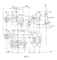
Specifically, as shown in FIG. 2, in the gate driving circuit according to embodiments of the present disclosure,
the pulling-up node potential pulling-up module 101 includes:
a first pulling-up node potential pulling-up transistor T101, a gate electrode and a first electrode of which are connected to the start signal input end STV, and a second electrode of which is connected to the feedback module 162; and
a second pulling-up node potential pulling-up transistor T102, a gate electrode of which is connected to the first control clock input end CLKA, a first electrode of which is connected to the second electrode of the first pulling-up node potential pulling-up transistor T101, and a second electrode of which is connected to the pulling-up node Q;
the pulling-up node potential pulling-down module 102 includes:
a first pulling-up node potential pulling-down transistor T201, a gate electrode of which is connected to the first pulling-down node QB1, a first electrode of which is connected to the pulling-up node Q, and a second electrode of which is connected to the feedback module 162;
a second pulling-up node potential pulling-down transistor T202, a gate electrode of which is connected to the first pulling-down node QB1, a first electrode of which is connected to the second electrode of the first pulling-up node potential pulling-down transistor T201, and a second electrode of which is connected with the first low level VGL1;
a third pulling-up node potential pulling-down transistor T203, a gate electrode of which is connected to the second pulling-down node QB2, a first electrode of which is connected to the pulling-up node Q, and a second electrode of which is connected to the feedback module 162; and
a fourth pulling-up node potential pulling-down transistor T204, a gate electrode of which is connected to the second pulling-down node QB2, a first electrode of which is connected to the second electrode of the third pulling-up node potential pulling-down transistor T203, and a second electrode of which is connected with the first low level VGL1;
the first pulling-down node potential pulling-down module 12 includes:
a first pulling-down transistor T21, a gate electrode of which is connected to the pulling-up node Q, a first electrode of which is connected to the first pulling-down node QB1, and a second electrode of which is connected to the reset signal input end RESET;
a second pulling-down transistor T22, a gate electrode of which is connected to the pulling-up node Q, a first electrode of which is connected to the second electrode of the first pulling-down transistor T21, and a second electrode of which is being connected with the first low level VGL1; and
a third pulling-down transistor T23, a gate electrode of which is connected to the second pulling-down node QB2, a first electrode of which is connected to the first pulling-down node QB1, and a second electrode of which is connected with the first low level VGL1;
the second pulling-down node potential pulling-down module 13 includes:
a fourth pulling-down transistor T31, a gate electrode of which is connected to the pulling-up node Q, a first electrode of which is connected to the second pulling-down node QB2, and a second electrode of which is connected to the reset signal input end RESET;
a fifth pulling-down transistor T32, a gate electrode of which is connected to the pulling-up node Q, a first electrode of which is connected to the second electrode of the third pulling-down transistor T31, and a second electrode of which is connected with the first low level VGL1; and
a sixth pulling-down transistor T33, a gate electrode of which is connected to the first pulling-down node QB1, a first electrode of which is connected to the second pulling-down node QB2, and a second electrode of which is connected with the first low level VGL1.
As shown in FIG. 2, the carry control module 151 includes:
a carry control transistor T51, a gate electrode of which is connected to the pulling-up node Q, a first electrode of which is connected to the second control clock input end CLKB, and a second end of which is connected to the carry signal output end COUT (n);
the carry signal pulling-down module 152 includes:
a first carry signal pulling-down transistor T521, a gate electrode of which is connected to the first pulling-down node QB1, a first electrode of which is connected to the carry signal output end COUT (n), and a second electrode of which is connected with the first low level VGL1; and
a second carry signal pulling-down transistor T522, a gate electrode of which is connected to the second pulling-down node QB2, a first electrode of which is connected to the carry signal output end COUT (n), and a second electrode of which is connected with the first low level VGL1;
the cutting-off control module 161 includes:
a first cutting-off control transistor T611, a gate electrode of which is connected to the pulling-up node Q, a first electrode of which is connected to the second control clock input end CLKB, and a second electrode of which is connected to the cutting-off control signal output end IOFF (n);
a second cutting-off control transistor T612, a gate electrode of which is connected to the first pulling-down node QB1, a first electrode of which is connected to the cutting-off control signal output end IOFF (n), and a second electrode of which is connected with the second low level VGL2; and
a third cutting-off control transistor T613, a gate electrode of which is connected to the second pulling-down node QB2, a first electrode of which is connected to the cutting-off control signal output end IOFF (n), and a second electrode of which is connected with the second low level VGL2;
the feedback module 162 includes:
a feedback transistor T62, a gate electrode of which is connected to the carry signal output end COUT (n), a first electrode of which is connected to the second electrode of the first pulling-up node potential pulling-up transistor T101, and a second electrode of which is connected to the cutting-off control signal output end IOFF (n).
As shown in FIG. 2, the gate scanning signal control module 171 includes:
a gate scanning control transistor T71, a gate electrode of which is connected to the pulling-up node Q, a first electrode of which is connected with the second control clock signal CLKB, and a second electrode of which is connected to the gate scanning signal output end GO_S1 (n);
the gate scanning signal pulling-down module 172 includes:
a first output pulling-down transistor T721, a gate electrode of which is connected to the first pulling-down node QB1, a first electrode of which is connected to the gate scanning signal output end GO_S1 (n), and a second electrode of which is connected with the second low level VGL2; and
a second output pulling-down transistor T722, a gate electrode of which is connected to the second pulling-down node QB2, a first electrode of which is connected to the gate scanning signal output end GO_S1 (n), and a second electrode of which is connected with the second low level VGL2;
the input clock switch 181 includes:
an input transistor T81, a gate electrode of which is connected to the pulling-up node Q, a first electrode of which is connected to an input clock end CLKIN, a second electrode of which is connected to the output level pulling-down control end G_VDD;
the output level pulling-up module 182 includes:
an output level pulling-up transistor T82, a gate electrode and first electrode of which are connected with a high level VDD, and a second electrode of which is connected to the output level end GO_ELVDD (n);
the output level pulling-down control module 183 includes:
a first pulling-down control transistor T831, a gate electrode of which is connected to the first pulling-down node QB1, a first electrode of which is connected to the output level pulling-down control end G_VDD, and a second electrode of which is connected with the second low level VGL2; and
a second pulling-down control transistor T832, a gate electrode of which is connected to the second pulling-down node QB2, a first electrode of which is connected to the output level pulling-down control end G_VDD, and a second electrode of which is connected with the second low level VGL2;
the output level pulling-down module 184 includes:
an output level pulling-down transistor T84, a gate electrode of which is connected to the output level pulling-down control end G_VDD, a first electrode of which is connected to the output level end GO_ELVDD (n), and a second electrode of which is connected with the second low level VGL2.
When implemented, the first control clock signal and second control clock signal may be inverted.
As shown in FIG. 2, the first control clock switch 141 includes:
a first control transistor T41, a gate electrode and a first electrode of which are connected to the first control clock input end CLKA, and a second electrode of which is connected to the first pulling-down node QB1.
The second control clock switch 142 includes:
a second control transistor T42, a gate electrode and a first electrode of which are connected to the second control clock input end CLKB, and a second electrode of which is connected to the second pulling-down node QB2.
The storage capacitor C is connected between the pulling-up node Q and the carry signal output end COUT (n).
In the embodiment as shown in FIG. 2, T101, T102, T42, T201, T202, T203 and T204 are P-type transistors, T21, T22, T31, T32, T41, T51, T521, T522, T611, T612, T613, T62, T71, T721, T722, T81, T82, T831, T832 and T84 are N-type transistors. In other embodiments, the type of the transistors can be changed as long as they can achieve the same effect of controlling the connection and disconnection.
An embodiment of the present disclosure further provides a gate driving method, applied in the above gate driving circuits, including:
pulling, by the second control clock switch, the potential of the second pulling-down node up to a high level; pulling, by the pulling-up node potential pulling-down module, the potential of the pulling-up node down to the first low level; pulling, by the first pulling-down node potential pulling-down module, the potential of the first pulling-down node down to the first low level; controlling, by output level pulling-up module, the output level end to output a high level; and controlling, by the gate scanning signal pulling-down module, the gate scanning signal output end to output the second low level, in a first stage, during which the start signal is of a low level, the first control clock signal is of a low level, the second control clock signal is of a high level;
pulling, by the pulling-up node potential pulling-up module, the potential of the pulling-up node up to a high level; pulling, by the first pulling-down node potential pulling-down module, the potential of the first pulling-down node down to the first low level; pulling, by the second pulling-down node potential pulling-down module, the potential of the second pulling-down node down to the first low level; and turning on the input clock switch, in a second stage, during which the start signal is of a high level, the first control clock signal is of a high level, the second control clock signal is of a low level, the input clock signal is of a low level, and the signals outputted by the output level end and gate scanning signal output end remain the same;
maintaining the potential of the pulling-up node at a high level; pulling, by the first pulling-down node potential pulling-down module, the potential of the first pulling-down node down to the first low level; pulling, by the second pulling-down node potential pulling-down module, the potential of the second pulling-down node down to the first low level; turning on the input clock switch; outputting, by the gate scanning signal output end, a high level; outputting, by the output level pulling-down control end, a high level; and controlling, by the output level pulling-down module, the output level end to output the second low level, in a third stage, during which the start signal is of a low level, the first control clock signal is of a low level, the second control clock signal is of a high level, and the input clock signal is of a high level;
pulling, by the pulling-up node potential pulling-down module, the potential of the pulling-up node down to the first low level; turning on the second control clock switch, thereby pulling the potential of the second pulling-down node up to a high level; pulling, by the first pulling-down node potential pulling-down module, the potential of the first pulling-down node down to the first low level; turning off the input clock switch; pulling, by the gate scanning signal pulling-down module, the potential of the gate scanning signal down to the second low level; controlling, by the output level pulling-down control module, the output level pulling-down control end to output the second low level; and controlling, by the output level pulling-up module, the output level end to output a high level, in a fourth stage, during which the start signal is of a low level, the first control clock signal is of a high level, the second control clock signal is of a low level.
An embodiment of the present disclosure further provides a GOA circuit, including multi-level gate driving circuits described above;
each level gate driving circuit further includes a driving control signal output end;
the start signal input end of a first level gate driving circuit and the start signal input end of a second level gate driving circuit are inputted with the start signal;
the start signal input end of an N-th level gate driving circuit is connected to the carry signal output end of an (N−2)-th level gate driving circuit, where N is an integer greater than or equal to 3 and less than or equal to M, and M is a number of levels of the gate driving circuits included in the GOA circuit;
except for the last level gate driving circuit, the driving control signal output end of each level gate driving circuit is connected to the output level end of a next level gate driving circuit;
the reset signal input end of a K-th level gate driving circuit is connected to the cutting-off control signal output end of a (K+2)-th level gate driving circuit, where K is an integer greater than or equal to 1 and less than M−1;
the first control signal input ends of odd-number-level gate driving circuits are connected with a first external control signal, and the second control signal input ends of the odd-number-level gate driving circuits are connected with a second external control signal;
the first control signal input ends of even-number-level gate driving circuits are connected with a third external control signal, and the second control signal input ends of odd-number-level gate driving circuits are connected with a fourth external control signal.
Moreover, the third external control signal is of one clock cycle later than the first external control signal;
the fourth external control signal is of one clock cycle later than the second external control signal.
The input clock signal inputted to a 2n-th level gate driving circuit and the input clock signal inputted to a (2n+2)-th level gate driving circuit are inverted;
the input clock signal inputted to a (2n−1)-th level gate driving circuit and the input clock signal inputted to a (2n+1)-th level gate driving circuit are inverted;
the input clock signal inputted to the 2n-th level gate driving circuit is of one clock cycle later than the input clock signal inputted to the (2n−1)-th level gate driving circuit; where n is an integer greater than or equal to 1, and 2n+2 is less than or equal to M.
In the GOA circuit according to the present disclosure, the driving control signal of each level gate driving circuit and the output level of next gate driving circuit use a same signal, which can simplify the circuit.
As shown in FIG. 3, according to a specific embodiment, the GOA circuit includes (N+1) level gate driving circuit, where N is an integer greater than or equal to 7;
a start signal input end STV of a first level gate driving circuit is inputted with the first start signal STV1;
a start signal input end STV of a second level gate driving circuit is inputted with the second start signal STV2;
a start signal input end STV of an M-th level gate driving circuit is connected to a carry signal output end COUT (M−1) of an (M−1)-th level gate driving circuit, where M is greater than 2 and less than (N+1);
    • except for a (N+1)th level gate driving circuit, a driving control signal output end IOFF (J) of a J-th level gate driving circuit is connected to an output level end GO_ELVDD (J+1) of a (J+1) level gate driving circuit, where J is a positive integer less than (N+1);
a reset signal input end RESET (K) of a K-th level gate driving circuit is connected to a cutting-off control signal output end IOFF (K+2) of a (K+2)-th level gate driving circuit, where K is an integer greater than or equal to 1 and less than N;
first control clock input ends CLKA of odd-number-level gate driving circuits are connected with a first control clock signal CLK1, and second control clock input ends CLKB of odd-number-level gate driving circuits are connected with a second control clock signal CLK2; CLK1 and CLK2 are inverted;
first control clock input ends CLKA of even-number-level gate driving circuits are connected with a third control clock signal CLK3, and second control clock input ends CLKB of even-number-level gate driving circuits are connected with a fourth control clock signal CLK4; CLK3 and CLK4 are inverted;
the third external control signal CLK3 is of one clock cycle later than the first external control signal CLK1;
the fourth external control signal CLK4 is of one clock cycle later than the second external control signal CLK2;
an input clock end CLKIN of a (2n−1)-th level gate driving circuit is inputted with a first input clock signal CLKIN1;
an input clock signal end CLKIN of (2n+1)-th level gate driving circuit is inputted with a second input clock signal CLKIN2;
an input clock end CLKIN of a (2n)-th level gate driving circuit is inputted with a third input clock signal CLKIN3;
an input clock end CLKIN of a (2n+2)-th level gate driving circuit is inputted with a fourth input clock signal CLKIN4;
CLKIN1 and CLKIN2 are inverted;
CLKIN3 and CLKIN4 are inverted;
CLKIN3 is of one clock cycle later than CLKIN1;
CLKIN4 is of one clock cycle later than CLKIN2;
where n is an integer greater than or equal to 1, and 2n+2 is less than or equal to N+1.
FIG. 4A is a diagram showing timing sequences of GO_ELVDD (n), GO_S1 (n) and GO_S2 (n) outputted by an N-th row pixel driving module and DATA inputted to the N-th row pixel driving module; FIG. 4B is a diagram showing timing sequences of GO_ELVDD (n+1), GO_S1 (n+1) and GO_S2 (n+1) outputted by an (N+1)-th row pixel driving module and DATA inputted to the (N+1)-th row pixel driving module.
In the above embodiment, it is designed that CLKIN3 is of one clock cycle later than CLKIN1, and CLKIN4 is of one clock cycle later than CLKIN2, an object of which is to make a waveform of GO_ELVDD (n+1) and a waveform of GO_S2 (n) be the same (as shown in FIG. 4A and FIG. 4B); therefore, GC_ELVDD (n+1) of the (N+1)-th row pixel driving module and GO_S2 (n) of the N-th row pixel driving module can use a same signal, wherein n+1 is less than or equal to a level number of gate driving circuits included in the GOA circuit.
FIG. 5A is a diagram showing waveforms of STV1, STV2, CLK1, CLK2, CLK3, CLK4, CLKIN1, CLKIN2, CLKIN3 and CLKIN4 when a GOA circuit is working according to an embodiment of the present disclosure.
FIG. 5B is a diagram showing waveforms of GO_S1 (n), GO_S1 (n+1), GO_S1 (n+2), GO_S1 (n+3), GO_ELVDD (n), GOELVDD (n+1), GOELVDD (n+2) and GOELVDD (n+3) outputted by a GOA circuit according to an embodiment of the present disclosure, where n+3 is less than or equal to the level number of gate driving circuits included in the GOA circuit.
As shown in FIGS. 5A and 5B, when the gate driving circuit as shown in FIG. 2 is working,
pulling, by the second control clock switch 142, the potential of the second pulling-down node QB2 up to a high level; pulling, by the pulling-up node potential pulling-down module 102, the potential of the pulling-up node Q down to the first low level VGL1; pulling, by the first pulling-down node potential pulling-down module 12, the potential of the first pulling-down node QB1 down to the first low level VGL1; controlling, by output level pulling-up module 182, the output level end GO_ELVDD (n) to output a high level; and controlling, by the gate scanning signal pulling-down module 172, the gate scanning signal output end GO_S1 (n) to output the second low level VGL2, in a first stage P1, during which the start signal is of a low level, the first control clock signal is of a low level, the second control clock signal is of a high level;
pulling, by the pulling-up node potential pulling-up module 101, the potential of the pulling-up node Q up to a high level; pulling, by the first pulling-down node potential pulling-down module 12, the potential of the first pulling-down node QB1 down to the first low level VGL1; pulling, by the second pulling-down node potential pulling-down module 13, the potential of the second pulling-down node QB2 down to the first low level VGL1; and turning on the input clock switch 181, in a second stage P2, during which the start signal is of a high level, the first control clock signal is of a high level, the second control clock signal is of a low level, the input clock signal is of a low level, and the signals outputted by the output level end GO_ELVDD (n) and gate scanning signal output end GO_S1 (n) remain the same;
maintaining the potential of the pulling-up node at a high level; pulling, by the first pulling-down node potential pulling-down module 12, the potential of the first pulling-down node QB1 down to the first low level VGL1; pulling, by the second pulling-down node potential pulling-down module 13, the potential of the second pulling-down node QB2 down to the first low level VGL1; turning on the input clock switch 181; outputting, by the gate scanning signal output end GO_S1 (n), a high level; outputting, by the output level pulling-down control end G_VDD, a high level; and controlling, by the output level pulling-down module 184, the output level end GO_ELVDD (n) to output the second low level VGL2, in a third stage, during which the start signal is of a low level, the first control clock signal is of a low level, the second control clock signal is of a high level, and the input clock signal is of a high level;
pulling, by the pulling-up node potential pulling-down module 102, the potential of the pulling-up node Q down to the first low level VGL1; turning on the second control clock switch 142, thereby pulling the potential of the second pulling-down node QB2 up to a high level; pulling, by the first pulling-down node potential pulling-down module 12, the potential of the first pulling-down node QB1 down to the first low level VGL1; turning off the input clock switch 181; pulling, by the gate scanning signal pulling-down module 172, the potential of the gate scanning signal down to the second low level VGL2; controlling, by the output level pulling-down control module 183, the output level pulling-down control end G_VDD to output the second low level VGL2; and controlling, by the output level pulling-up module 182, the output level end GO_ELVDD (n) to output a high level, in a fourth stage, during which the start signal is of a low level, the first control clock signal is of a high level, the second control clock signal is of a low level.
As shown in FIGS. 5A and 5B, the timing sequences of a fifth stage P5, a sixth stage Pb, a seventh stage P7, and an eighth stage P8 are as same as the first stage P1, the second stage P2, the third stage P3, and the fourth stage P4.
The above gate driving circuit may be applied in OLED display devices and low-temperature polysilicon (LTPS) display devices.
The present disclosure further provides a display device, including the above gate driving circuit. The display device may be an OLED display device or an LTPS display device.
The above is only preferred embodiments of the present disclosure, it should be noted that several improvements and modifications may be made for those of ordinary skill in the art without departing from the principle of the present disclosure, and also should be considered to fall within the protection scope of the present disclosure.

Claims (18)

What is claimed is:
1. A gate driving circuit, connected to a row pixel circuit which comprises a row pixel driving circuit and a light emitting element connected to each other, the row pixel driving circuit comprising a driving transistor, a driving circuit and a compensation circuit, the compensation circuit being connected with a gate scanning signal, and the driving circuit being connected with a driving level; wherein
the gate driving circuit comprises a row pixel control circuit, which is configured to provide the gate scanning signal to the compensation circuit and provide the driving level to the driving circuit, so as to control the compensation circuit to compensate for a threshold voltage of the driving transistor and control the driving circuit to drive the light emitting element,
wherein the row pixel control circuit comprises a first control clock input end, a second control clock input end, a first control clock switch, and a second control clock switch;
wherein the first control clock switch is configured to set up a connection between the first control clock input end and a first pulling-down node, in response to the first control clock signal being of a high level;
wherein the second control clock switch is configured to set up a connection between the second control clock input end and a second pulling-down node, in response to a second control clock signal being of a high level; and
wherein the first control clock signal and the second control clock signal are inverted, while an output level at the first pulling-down node and an output level at the second pulling-down node are inverted.
2. The gate driving circuit according to claim 1, wherein the row pixel control circuit further comprises:
a start signal input end;
a reset signal input end;
an input clock end;
a carry signal output end;
a cutting-off control signal output end,
an output level end;
an output level pulling-down control end;
a gate scanning signal output end;
a pulling-up node potential pulling-up circuit, configured to pull a potential of a pulling-up node up to a high level, when a first control clock signal and a start signal are of a high level;
a storage capacitor, connected between the pulling-up node and the carry signal output end;
a pulling-up node potential pulling-down circuit, configured to pull the potential of the pulling-up node down to a first low level, when a potential of a first pulling-down node or a potential of a second pulling-down node is of a high level;
a first pulling-down node potential pulling-down circuit, configured to pull the potential of the first pulling-down node down to the first low level, when the potential of the pulling-up node or the potential of the second pulling-down node is of a high level;
a second pulling-down node potential pulling-down circuit, connected to the reset signal input end, configured to pull the potential of the second pulling-down node down to the first low level, when the potential of the pulling-up node or the potential of the first pulling-down node is of a high level;
a carry control circuit, configured to set up a connection between the carry signal output end and the second control clock input end, when the potential of the pulling-up node is of a high level;
a carry signal pulling-down circuit, configured to pull a potential of the carry signal down to the first low level, when the potential of the first pulling-down node or the potential of the second pulling-down node is of a high level;
a cutting-off control circuit, configured to set up a connection between the second control clock input end and the cutting-off control signal output end, when the potential of the pulling-up node is of a high level; and set up a connection between the cutting-off control signal output end and a second low Level output end, when the potential of the first pulling-down node or the potential of the second pulling-down node is of a high level;
a feedback circuit, configured to transmit a cutting-off control signal to the pulling-up node potential pulling-up circuit and the pulling-up node potential pulling-down circuit, when the carry signal is of a high level;
a gate scanning signal control circuit, configured to set up a connection between the second control clock input end and the gate scanning signal output end, when the potential of the pulling-up node is of a high level;
an input clock switch, configured to set up a connection between the input clock end and the output level pulling-down control end, when the potential of the pulling-up node is of a high level;
a gate scanning signal pulling-down circuit, configured to pull a potential of the gate scanning signal down to a second low level, when the potential of the first pulling-down node or the potential of the second pulling-down node is of a high level;
an output level pulling-down control circuit, configured to pull a potential of the output level pulling-down control end down to the second low level, when the potential of the first pulling-down node or the potential of the second pulling-down node is of a high level;
an output level pulling-up circuit, configured to pull the output level up to a high level, when an output level pulling-down control end outputs the second low level; and
an output level pulling-down circuit, configured to pull the output level down to the second low level, when the output level pulling-down control end outputs a high level.
3. The gate driving circuit according to claim 2, wherein
the pulling-up node potential pulling-up circuit comprises:
a first pulling-up node potential pulling-up transistor, a gate electrode and a first electrode of which are connected to the start signal input end, and a second electrode of which is connected to the feedback circuit; and
a second pulling-up node potential pulling-up transistor, a gate electrode of which is connected to the first control clock input end, a first electrode of which is connected to the second electrode of the first pulling-up node potential pulling-up transistor, and a second electrode of which is connected to the pulling-up node,
the pulling-up node potential pulling-down circuit comprises:
a first pulling-up node potential pulling-down transistor, a gate electrode of which is connected to the first pulling-down node, a first electrode of which is connected to the pulling-up node, and a second electrode of which is connected to the feedback circuit;
a second pulling-up node potential pulling-down transistor, a gate electrode of which is connected to the first pulling-down node, a first electrode of which is connected to the second electrode of the first pulling-up node potential pulling-down transistor, and a second electrode of which is connected with the first low level;
a third pulling-up node potential pulling-down transistor, a gate electrode of which is connected to the second pulling-down node, a first electrode of which is connected to the pulling-up node, and a second electrode of which is connected to the feedback circuit; and
a fourth pulling-up node potential pulling-down transistor, a gate electrode of which is connected to the second pulling-down node, a first electrode of which is connected to the second electrode of the third pulling-up node potential pulling-down transistor, and a second electrode of which is connected with the first low level,
the first pulling-down node potential pulling-down circuit comprises:
a first pulling-down transistor, a gate electrode of which is connected to the pulling-up node, a first electrode of which is connected to the first pulling-down node, and a second electrode of which is connected to the reset signal input end;
a second pulling-down transistor, a gate electrode of which is connected to the pulling-up node, a first electrode of which is connected to the second electrode of the first pulling-down transistor, and a second electrode of which is being connected with the first low level; and
a third pulling-down transistor, a gate electrode of which is connected to the second pulling-down node, a first electrode of which is connected to the first pulling-down node, and a second electrode of which is connected with the first low level;
the second pulling-down node potential pulling-down circuit comprises:
a fourth pulling-down transistor, a gate electrode of which is connected to the pulling-up node, a first electrode of which is connected to the second pulling-down node, and a second electrode of which is connected to the reset signal input end;
a fifth pulling-down transistor, a gate electrode of which is connected to the pulling-up node, a first electrode of which is connected to the second electrode of the fourth pulling-down transistor, and a second electrode of which is connected with the first low level; and
a sixth pulling-down transistor, a gate electrode of which is connected to the first pulling-down node, a first electrode of which is connected to the second pulling-down node, and a second electrode of which is connected with the first low level.
4. The gate driving circuit according to claim 3, wherein the carry control circuit comprises:
a carry control transistor, a gate electrode of which is connected to the pulling-up node, a first electrode of which is connected to the second control clock input end, and a second end of which is connected to the carry signal output end,
the carry signal pulling-down circuit comprises:
a first carry signal pulling-down transistor, a gate electrode of which is connected to the first pulling-down node, a first electrode of which is connected to the carry signal output end, and a second electrode of which is connected with the first low level; and
a second carry signal pulling-down transistor, a gate electrode of which is connected to the second pulling-down node, a first electrode of which is connected to the carry signal output end, and a second electrode of which is connected with the first low level,
the cutting-off control circuit comprises:
a first cutting-off control transistor, a gate electrode of which is connected to the pulling-up node, a first electrode of which is connected to the second control clock input end, and a second electrode of which is connected to the cutting-off control signal output end;
a second cutting-off control transistor, a gate electrode of which is connected to the first pulling-down node, a first electrode of which is connected to the cutting-off control signal output end, and a second electrode of which is connected with the second low level; and
a third cutting-off control transistor, a gate electrode of which is connected to the second pulling-down node, a first electrode of which is connected to the cutting-off control signal output end, and a second electrode of which is connected with the second low level,
the feedback circuit comprises:
a feedback transistor, a gate electrode of which is connected to the carry signal output end, a first electrode of which is connected to the second electrode of the first pulling-up node potential pulling-up transistor, and a second electrode of which is connected to the cutting-off control signal output end.
5. The gate driving circuit according to claim 4, wherein
the gate scanning signal control circuit comprises:
a gate scanning control transistor, a gate electrode of which is connected to the pulling-up node, a first electrode of which is connected with the second control clock signal, and a second electrode of which is connected to the gate scanning signal output end,
the gate scanning signal pulling-down circuit comprises:
a first output pulling-down transistor, a gate electrode of which is connected to the first pulling-down node, a first electrode of which is connected to the gate scanning signal output end, and a second electrode of which is connected with the second low level; and
a second output pulling-down transistor, a gate electrode of which is connected to the second pulling-down node, a first electrode of which is connected to the gate scanning signal output end, and a second electrode of which is connected with the second low level;
the output level pulling-up circuit comprises:
an output level pulling-up transistor, a gate electrode and first electrode of which are connected with a high level, and a second electrode of which is connected to the output level end,
the output level pulling-down control circuit comprises:
a first pulling-down control transistor, a gate electrode of which is connected to the first pulling-down node, a first electrode of which is connected to the output level pulling-down control end, and a second electrode of which is connected with the second low level; and
a second pulling-down control transistor, a gate electrode of which is connected to the second pulling-down node, a first electrode of which is connected to the output level pulling-down control end, and a second electrode of which is connected with the second low level,
the output level pulling-down circuit comprises:
an output level pulling-down transistor, a gate electrode of which is connected to the output level pulling-down control end, a first electrode of which is connected to the output level end, and a second electrode of which is connected with the second low level.
6. The gate driving circuit according to claim 4, wherein
the input clock switch comprises an input transistor, a gate electrode of which is connected to the pulling-up node, a first electrode of which is connected to the input clock end, and a second electrode of which is connected to output level pulling-down control end.
7. A gate driving method, applied in the gate driving circuit according to claim 2, the method comprising:
pulling, by the second control clock switch, the potential of the second pulling-down node up to a high level; pulling, by the pulling-up node potential pulling-down circuit, the potential of the pulling-up node down to the first low level; pulling, by the first pulling-down node potential pulling-down circuit, the potential of the first pulling-down node down to the first low level; controlling, by output level pulling-up circuit, the output level end to output a high level; and controlling, by the gate scanning signal pulling-down circuit, the gate scanning signal output end to output the second low level, in a first stage, during which the start signal is of a low level, the first control clock signal is of a low level, the second control clock signal is of a high level;
pulling, by the pulling-up node potential pulling-up circuit, the potential of the pulling-up node up to a high level; pulling, by the first pulling-down node potential pulling-down circuit, the potential of the first pulling-down node down to the first low level; pulling, by the second pulling-down node potential pulling-down circuit, the potential of the second pulling-down node down to the first low level; and turning on the input clock switch, in a second stage, during which the start signal is of a high level, the first control clock signal is of a high level, the second control clock signal is of a low level, an input clock signal is of a low level, and the signals outputted by the output level end and gate scanning signal output end remain the same;
maintaining the potential of the pulling-up node at a high level; pulling, by the first pulling-down node potential pulling-down circuit, the potential of the first pulling-down node down to the first low level; pulling, by the second pulling-down node potential pulling-down circuit, the potential of the second pulling-down node down to the first low level; turning on the input clock switch; outputting, by the gate scanning signal output end, a high level; outputting, by the output level pulling-down control end, a high level; and controlling, by the output level pulling-down circuit, the output level end to output the second low level, in a third stage, during which the start signal is of a low level, the first control clock signal is of a low level, the second control clock signal is of a high level, and the input clock signal is of a high level; and
pulling, by the pulling-up node potential pulling-down circuit, the potential of the pulling-up node down to the first low level; turning on the second control clock switch, thereby pulling the potential of the second pulling-down node up to a high level; pulling, by the first pulling-down node potential pulling-down circuit, the potential of the first pulling-down node down to the first low level; turning off the input clock switch; pulling, by the gate scanning signal pulling-down circuit, the potential of the gate scanning signal down to the second low level; controlling, by the output level pulling-down control circuit, the output level pulling-down control end to output the second low level; and controlling, by the output level pulling-up circuit, the output level end to output a high level, in a fourth stage, during which the start signal is of a low level, the first control clock signal is of a high level, the second control clock signal is of a low level.
8. A Gate on array (GOA) circuit, comprising multi-level gate driving circuits according to claim 1; wherein
each level gate driving circuit further comprises a driving control signal output end;
a start signal input end of a first level gate driving circuit and a start signal input end of a second level gate driving circuit are inputted with a start signal;
a start signal input end of an N-th level gate driving circuit is connected to a carry signal output end of an (N−2)-th level gate driving circuit, where N is an integer greater than or equal to 3 and less than or equal to M, and M is a number of levels of the gate driving circuits included in the GOA circuit;
except for a last level gate driving circuit, the driving control signal output end of each level gate driving circuit is connected to the output level end of a next level gate driving circuit;
a reset signal input end of a K-th level gate driving circuit is connected to a cutting-off control signal output end of a (K+2)-th level gate driving circuit, where K is an integer greater than or equal to 1 and less than M−1;
a first control signal input ends of odd-number-level gate driving circuits are connected with a first external control signal, and a second control signal input ends of the odd-number-level gate driving circuits are connected with a second external control signal; and
a first control signal input ends of even-number-level gate driving circuits are connected with a third external control signal, and a second control signal input ends of odd-number-level gate driving circuits are connected with a fourth external control signal.
9. The GOA circuit according to claim 8, wherein
the first external control signal and the second external control signal are inverted;
the third external control signal and the fourth external control signal are inverted.
10. The GOA circuit according to claim 8, wherein
the third external control signal is of one clock cycle later than the first external control signal;
the fourth external control signal is of one clock cycle later than the second external control signal.
11. The GOA circuit according to claim 8, wherein
an input clock signal inputted to a 2n-th level gate driving circuit and an input clock signal inputted to a (2n+2)-th level gate driving circuit are inverted;
an input clock signal inputted to a (2n−1)-th level gate driving circuit and an input clock signal inputted to a (2n+1)-th level gate driving circuit are inverted;
the input clock signal inputted to the 2n-th level gate driving circuit is of one clock cycle later than the input clock signal inputted to the (2n−1)-th level gate driving circuit;
the input clock signal inputted to the (2n+2)-th level gate driving circuit is of one clock cycle later than the input clock signal inputted to the (2n+1)-th level gate driving circuit;
where n is an integer greater than or equal to 1, and 2n+2 is less than or equal to M.
12. A display device, comprising a gate driving circuit, wherein the gate driving circuit is connected to a row pixel circuit, which comprises a row pixel driving circuit and a light emitting element connected to each other, the row pixel driving circuit comprising a driving transistor, a driving circuit and a compensation circuit, the compensation circuit being connected with a gate scanning signal and the driving circuit being connected with a driving level; wherein
the gate driving circuit comprises a row pixel control circuit, which is configured to provide the gate scanning signal to the compensation circuit and provide the driving level to the driving circuit, so as to control the compensation circuit to compensate for a threshold voltage of the driving transistor and control the driving circuit to drive the light emitting element,
wherein the row pixel control circuit comprises a first control clock input end, a second control clock input end, a first control clock switch, and a second control clock switch;
wherein the first control clock switch is configured to set up a connection between the first control clock input end and the first pulling-down node, in response to the first control clock signal being of a high level;
wherein the second control clock switch is configured to set up a connection between the second control clock input end and the second pulling-down node, in response to a second control clock signal being of a high level; and
wherein the first control clock signal and the second control clock signal are inverted, while an output level at the first pulling-down node and an output level at the second pulling-down node are inverted.
13. The display device according to claim 12, wherein the row pixel control circuit further comprises:
a start signal input end;
a reset signal input end;
an input clock end;
a carry signal output end;
a cutting-off control signal output end;
an output level end;
an output level pulling-down control end;
a gate scanning signal output end;
a pulling-up node potential pulling-up circuit, configured to pull a potential of a pulling-up node up to a high level, when a first control clock signal and a start signal are of a high level;
a storage capacitor, connected between the pulling-up node and the carry signal output end;
a pulling-up node potential pulling-down circuit, configured to pull the potential of the pulling-up node down to a first low level, when a potential of a first pulling-down node or a potential of a second pulling-down node is of a high level;
a first pulling-down node potential pulling-down circuit, configured to pull the potential of the first pulling-down node down to the first low level, when the potential of the pulling-up node or the potential of the second pulling-down node is of a high level;
a second pulling-down node potential pulling-down circuit, connected to the reset signal input end, configured to pull the potential of the second pulling-down node down to the first low level, when the potential of the pulling-up node or the potential of the first pulling-down node is of a high level;
a carry control circuit, configured to set up a connection between the carry signal output end and the second control clock input end, when the potential of the pulling-up node is of a high level;
a carry signal pulling-down circuit, configured to pull a potential of the carry signal down to the first low level, when the potential of the first pulling-down node or the potential of the second pulling-down node is of a high level;
a cutting-off control circuit, configured to set up a connection between the second control clock input end and the cutting-off control signal output end, when the potential of the pulling-up node is of a high level; and set up a connection between the cutting-off control signal output end and a second low level output end, when the potential of the first pulling-down node or the potential of the second pulling-down node is of a high level;
a feedback circuit, configured to transmit a cutting-off control signal to the pulling-up node potential pulling-up circuit and the pulling-up node potential pulling-down circuit, when the carry signal is of a high level;
a gate scanning signal control circuit, configured to set up a connection between the second control clock input end and the gate scanning signal output end, when the potential of the pulling-up node is of a high level;
an input clock switch, configured to set up a connection between the input clock end and the output level pulling-down control end, when the potential of the pulling-up node is of a high level;
a gate scanning signal pulling-down circuit, configured to pull a potential of the gate scanning signal down to a second low level, when the potential of the first pulling-down node or the potential of the second pulling-down node is of a high level;
an output level pulling-down circuit, configured to pull a potential of the output level pulling-down control end down to the second low level, when the potential of the first pulling-down node or the potential of the second pulling-down node is of a high level;
an output level pulling-up circuit, configured to pull the output level up to a high level, when an output level pulling-down control end outputs the second low level; and
an output level pulling-down circuit, configured to pull the output level down to the second low level, when the output level pulling-down control end outputs a high level.
14. The display device according to claim 13, wherein
the pulling-up node potential pulling-up circuit comprises:
a first pulling-up node potential pulling-up transistor, a gate electrode and a first electrode of which are connected to the start signal input end, and a second electrode of which is connected to the feedback circuit; and
a second pulling-up node potential pulling-up transistor, a gate electrode of which is connected to the first control clock input end, a first electrode of which is connected to the second electrode of the first pulling-up node potential pulling-up transistor, and a second electrode of which is connected to the pulling-up node,
the pulling-up node potential pulling-down circuit comprises:
a first pulling-up node potential pulling-down transistor, a gate electrode of which is connected to the first pulling-down node, a first electrode of which is connected to the pulling-up node, and a second electrode of which is connected to the feedback circuit;
a second pulling-up node potential pulling-down transistor, a gate electrode of which is connected to the first pulling-down node, a first electrode of which is connected to the second electrode of the first pulling-up node potential pulling-down transistor, and a second electrode of which is connected with the first low level;
a third pulling-up node potential pulling-down transistor, a gate electrode of which is connected to the second pulling-down node, a first electrode of which is connected to the pulling-up node, and a second electrode of which is connected to the feedback circuit; and
a fourth pulling-up node potential pulling-down transistor, a gate electrode of which is connected to the second pulling-down node, a first electrode of which is connected to the second electrode of the third pulling-up node potential pulling-down transistor, and a second electrode of which is connected with the first low level,
the first pulling-down node potential pulling-down circuit comprises:
a first pulling-down transistor, a gate electrode of which is connected to the pulling-up node, a first electrode of which is connected to the first pulling-down node, and a second electrode of which is connected to the reset signal input end;
a second pulling-down transistor, a gate electrode of which is connected to the pulling-up node, a first electrode of which is connected to the second electrode of the first pulling-down transistor, and a second electrode of which is being connected with the first low level; and
a third pulling-down transistor, a gate electrode of which is connected to the second pulling-down node, a first electrode of which is connected to the first pulling-down node, and a second electrode of which is connected with the first low level,
the second pulling-down node potential pulling-down circuit comprises:
a fourth pulling-down transistor, a gate electrode of which is connected to the pulling-up node, a first electrode of which is connected to the second pulling-down node, and a second electrode of which is connected to the reset signal input end;
a fifth pulling-down transistor, a gate electrode of which is connected to the pulling-up node, a first electrode of which is connected to the second electrode of the fourth pulling-down transistor, and a second electrode of which is connected with the first low level; and
a sixth pulling-down transistor, a gate electrode of which is connected to the first pulling-down node, a first electrode of which is connected to the second pulling-down node, and a second electrode of which is connected with the first low level.
15. The display device according to claim 14, wherein
the carry control circuit comprises:
a carry control transistor, a gate electrode of which is connected to the pulling-up node, a first electrode of which is connected to the second control clock input end, and a second end of which is connected to the carry signal output end,
the carry signal pulling-down circuit comprises:
a first carry signal pulling-down transistor, a gate electrode of which is connected to the first pulling-down node, a first electrode of which is connected to the carry signal output end, and a second electrode of which is connected with the first low level; and
a second carry signal pulling-down transistor, a gate electrode of which is connected to the second pulling-down node, a first electrode of which is connected to the carry signal output end, and a second electrode of which is connected with the first low level,
the cutting-off control circuit comprises:
a first cutting-off control transistor, a gate electrode of which is connected to the pulling-up node, a first electrode of which is connected to the second control clock input end, and a second electrode of which is connected to the cutting-off control signal output end;
a second cutting-off control transistor, a gate electrode of which is connected to the first pulling-down node, a first electrode of which is connected to the cutting-off control signal output end, and a second electrode of which is connected with the second low level; and
a third cutting-off control transistor, a gate electrode of which is connected to the second pulling-down node, a first electrode of which is connected to the cutting-off control signal output end, and a second electrode of which is connected with the second low level,
the feedback circuit comprises:
a feedback transistor, a gate electrode of which is connected to the carry signal output end, a first electrode of which is connected to the second electrode of the first pulling-up node potential pulling-up transistor, and a second electrode of which is connected to the cutting-off control signal output end.
16. The display device according to claim 15, wherein
the gate scanning signal control circuit comprises:
a gate scanning control transistor, a gate electrode of which is connected to the pulling-up node, a first electrode of which is connected with the second control clock signal, and a second electrode of which is connected to the gate scanning signal output end,
the gate scanning signal pulling-down circuit comprises:
a first output pulling-down transistor, a gate electrode of which is connected to the first pulling-down node, a first electrode of which is connected to the gate scanning signal output end, and a second electrode of which is connected with the second low level; and
a second output pulling-down transistor, a gate electrode of which is connected to the second pulling-down node, a first electrode of which is connected to the gate scanning signal output end, and a second electrode of which is connected with the second low level,
the output level pulling-up circuit comprises:
an output level pulling-up transistor, a gate electrode and first electrode of which are connected with a high level, and a second electrode of which is connected to the output level end,
the output level pulling-down control circuit comprises:
a first pulling-down control transistor, a gate electrode of which is connected to the first pulling-down node, a first electrode of which is connected to the output level pulling-down control end, and a second electrode of which is connected with the second low level; and
a second pulling-down control transistor, a gate electrode of which is connected to the second pulling-down node, a first electrode of which is connected to the output level pulling-down control end, and a second electrode of which is connected with the second low level,
the output level pulling-down circuit comprises:
an output level pulling-down transistor, a gate electrode of which is connected to the output level pulling-down control end, a first electrode of which is connected to the output level end, and a second electrode of which is connected with the second low level.
17. The display device according to claim 15, wherein
the input clock switch comprises an input transistor, a gate electrode of which is connected to the pulling-up node, a first electrode of which is connected to the input clock end, and a second electrode of which is connected to output level pulling-down control end.
18. The display device according to claim 12, wherein the display device is an organic light-emitting diode (OLED) display device or a low-temperature polysilicon (LTPS) display device.
US14/415,082 2013-12-26 2014-05-29 Gate driving circuit, gate driving method, gate on array (GOA) circuit and display device Active 2034-06-11 US9514683B2 (en)

Applications Claiming Priority (4)

Application Number Priority Date Filing Date Title
CN201310738811 2013-12-26
CN201310738811.7A CN103730089B (en) 2013-12-26 2013-12-26 Gate driver circuit, method, array base palte horizontal drive circuit and display device
CN201310738811.7 2013-12-26
PCT/CN2014/078725 WO2015096387A1 (en) 2013-12-26 2014-05-29 Gate drive circuit, method, gate on array circuit and display apparatus

Publications (2)

Publication Number Publication Date
US20160019840A1 US20160019840A1 (en) 2016-01-21
US9514683B2 true US9514683B2 (en) 2016-12-06

Family

ID=50454139

Family Applications (1)

Application Number Title Priority Date Filing Date
US14/415,082 Active 2034-06-11 US9514683B2 (en) 2013-12-26 2014-05-29 Gate driving circuit, gate driving method, gate on array (GOA) circuit and display device

Country Status (3)

Country Link
US (1) US9514683B2 (en)
CN (1) CN103730089B (en)
WO (1) WO2015096387A1 (en)

Cited By (1)

* Cited by examiner, † Cited by third party
Publication number Priority date Publication date Assignee Title
US10566071B2 (en) * 2017-09-30 2020-02-18 Boe Technology Group Co., Ltd. Shift register unit, method for driving shift register unit, gate driving circuit and display device

Families Citing this family (24)

* Cited by examiner, † Cited by third party
Publication number Priority date Publication date Assignee Title
CN103714780B (en) 2013-12-24 2015-07-15 京东方科技集团股份有限公司 Grid driving circuit, grid driving method, array substrate row driving circuit and display device
CN103730089B (en) * 2013-12-26 2015-11-25 京东方科技集团股份有限公司 Gate driver circuit, method, array base palte horizontal drive circuit and display device
CN103714781B (en) * 2013-12-30 2016-03-30 京东方科技集团股份有限公司 Gate driver circuit, method, array base palte horizontal drive circuit and display device
CN104157236B (en) * 2014-07-16 2016-05-11 京东方科技集团股份有限公司 A kind of shift register and gate driver circuit
CN104409038B (en) * 2014-11-25 2017-05-24 北京大学深圳研究生院 Gate drive circuit, unit thereof and AMOLED display
CN104616616B (en) * 2015-02-12 2017-12-15 京东方科技集团股份有限公司 Gate driving circuit and its driving method, array base palte, display device
CN105139825B (en) * 2015-10-20 2017-08-25 京东方科技集团股份有限公司 Shift register cell, gate drive apparatus, display device, control method
KR102555084B1 (en) * 2015-12-30 2023-07-13 엘지디스플레이 주식회사 Module for driving gate and gate in panel
CN105609135B (en) * 2015-12-31 2019-06-11 京东方科技集团股份有限公司 Shift register unit and driving method thereof, gate driving circuit and display device
CN106205461B (en) * 2016-09-30 2019-04-02 京东方科技集团股份有限公司 Shift register unit, driving method, gate driving circuit and display device
CN106448595B (en) * 2016-10-24 2018-11-09 南京华东电子信息科技股份有限公司 A kind of gate driving circuit of high reliability
CN106710550B (en) * 2016-12-30 2019-03-19 深圳市华星光电技术有限公司 A kind of GOA cascade circuit for large size panel
KR102445577B1 (en) * 2017-10-27 2022-09-20 엘지디스플레이 주식회사 Gate driver and display device including same
CN108877713B (en) * 2018-07-17 2020-06-12 惠科股份有限公司 Display device and shift register circuit
CN109712581B (en) * 2019-01-02 2021-01-29 京东方科技集团股份有限公司 Common voltage compensation circuit, display driver and display device
CN109817153B (en) * 2019-04-15 2022-04-29 合肥鑫晟光电科技有限公司 Gate driving unit, gate driving method, gate driving circuit and display device
CN110675828A (en) * 2019-09-10 2020-01-10 深圳市华星光电半导体显示技术有限公司 GOA circuit
CN111210759B (en) * 2020-02-28 2023-06-20 京东方科技集团股份有限公司 Shift register unit, gate driving circuit and display device
CN111223452B (en) 2020-03-18 2021-07-23 深圳市华星光电半导体显示技术有限公司 GOA circuit
CN112365851A (en) * 2020-11-13 2021-02-12 深圳市华星光电半导体显示技术有限公司 GOA circuit and display panel
CN113689824B (en) * 2021-09-06 2022-12-23 深圳市华星光电半导体显示技术有限公司 Emission control driver and display device
CN115966169B (en) * 2021-10-08 2024-07-26 乐金显示有限公司 Gate driver and display device including the same
CN115171610B (en) * 2022-07-28 2023-05-26 惠科股份有限公司 Driving circuit and display panel
CN116543691B (en) * 2023-05-19 2024-04-02 华南理工大学 Gate driving circuit, active electroluminescent display and driving method

Citations (52)

* Cited by examiner, † Cited by third party
Publication number Priority date Publication date Assignee Title
CN1684558A (en) 2004-04-12 2005-10-19 三洋电机株式会社 Organic EL pixel circuit
US20060038500A1 (en) 2004-08-19 2006-02-23 Lee Jong-Hwan Driving circuit for display device
KR20060091465A (en) 2005-02-15 2006-08-21 삼성전자주식회사 Gate driving circuit and display device having same
US20060202977A1 (en) 2005-03-14 2006-09-14 Lg Philips Lcd Co., Ltd. Organic electroluminescent display device and driving method thereof
US20060291610A1 (en) 2005-06-28 2006-12-28 Wintek Corporation High-stability shift circuit using amorphous silicon thin film transistors
US20070091029A1 (en) * 2003-12-02 2007-04-26 Sony Corporation Transistor circuit, pixel circuit, display device, and driving method therefor
JP2007140318A (en) 2005-11-22 2007-06-07 Sony Corp Pixel circuit
US20070296662A1 (en) 2006-06-21 2007-12-27 Lee Min-Cheol Gate driving circuit and display apparatus having the same
CN101097677A (en) 2006-06-30 2008-01-02 索尼株式会社 Display device and driving method thereof
CN101122720A (en) 2006-08-08 2008-02-13 三星电子株式会社 Gate driver and display device having same
CN101183508A (en) 2006-11-13 2008-05-21 索尼株式会社 Display device, method for driving same, and electronic device
US7382347B2 (en) 2001-04-13 2008-06-03 Kabushiki Kaisha Toshiba Shift register for pulse-cut clock signal
CN101271667A (en) 2007-03-22 2008-09-24 索尼株式会社 Display device, driving method thereof, and electronic device
CN101276547A (en) 2007-03-26 2008-10-01 索尼株式会社 Display device, method for driving display device, and electronic device
CN101339737A (en) 2008-08-11 2009-01-07 上海广电光电子有限公司 Pixel circuit of active organic light-emitting device
CN101364392A (en) 2007-08-06 2009-02-11 三星电子株式会社 Gate driving circuit and display device having the gate driving circuit
US20090135166A1 (en) 2007-11-28 2009-05-28 Sony Corporation Display apparatus and fabrication method and fabrication apparatus for the same
CN101556762A (en) 2008-04-09 2009-10-14 索尼株式会社 Image display device and driving method of image display device
CN101556763A (en) 2008-04-09 2009-10-14 索尼株式会社 Image display device and driving method of image display device
US20100134469A1 (en) * 2008-11-28 2010-06-03 Casio Computer Co., Ltd. Light emitting device and a drive control method for driving a light emitting device
CN101770745A (en) 2008-12-17 2010-07-07 索尼株式会社 Display device, display device drive method, and electronic apparatus
US20100182227A1 (en) 2009-01-16 2010-07-22 Yuan-Hsin Tsou Gate driving circuit capable of suppressing threshold voltage drift
US20100188385A1 (en) * 2007-07-24 2010-07-29 Koninklijke Philips Electronics N.V. Shift register circuit having threshold voltage compensation
US20100201659A1 (en) 2009-02-12 2010-08-12 Semiconductor Energy Laboratory Co., Ltd. Pulse output circuit, display device, and electronic device
US20100207667A1 (en) 2009-02-17 2010-08-19 Kwon Yeong-Keun Method of driving gate lines, gate line drive circuit for performing the method and display device having the gate line drive circuit
EP2237253A1 (en) 2009-04-01 2010-10-06 ARISTOTLE UNIVERSITY OF THESSALONIKI- Research Committee Pixel circuit, display using the same and driving method for the same
US20110157112A1 (en) 2009-12-25 2011-06-30 Hitachi Displays, Ltd. Gate signal line driving circuit and display device
US20110164071A1 (en) 2010-01-04 2011-07-07 Bo-Yong Chung Pixel circuit, organic electro-luminescent display apparatus, and method of driving the same
US20110279429A1 (en) 2010-05-12 2011-11-17 Kwi Hyun Kim Display device
CN102298900A (en) 2010-06-28 2011-12-28 三星移动显示器株式会社 Organic light emitting display and driving method thereof
CN102592561A (en) 2011-12-29 2012-07-18 友达光电股份有限公司 Gate drive circuit
CN102654972A (en) 2011-06-21 2012-09-05 京东方科技集团股份有限公司 Active matrix organic light emitting diode (AMOLED) and drive circuit and method of AMOLED
CN102708824A (en) 2012-05-31 2012-10-03 京东方科技集团股份有限公司 Threshold voltage offset compensation circuit for thin film transistor, gate on array (GOA) circuit and display
US8289261B2 (en) 2008-08-14 2012-10-16 Samsung Display Co., Ltd. Gate driving circuit and display device having the same
US20120287103A1 (en) * 2011-05-13 2012-11-15 Boe Technology Group Co., Ltd. Pixel unit circuit, pixel array, display panel and display panel driving method
CN102930822A (en) 2012-11-12 2013-02-13 京东方科技集团股份有限公司 Pixel circuit and display device and driving method of pixel circuit
CN102956269A (en) 2012-07-05 2013-03-06 友达光电股份有限公司 Shift register
CN103218970A (en) 2013-03-25 2013-07-24 京东方科技集团股份有限公司 Active matrix organic light emitting diode (AMOLED) pixel unit, driving method and display device
CN103236236A (en) 2013-04-24 2013-08-07 京东方科技集团股份有限公司 Pixel driving circuit, array substrate and display device
US20130307840A1 (en) * 2008-12-05 2013-11-21 Samsung Display Co., Ltd. Display device and method of driving the same
CN103440840A (en) 2013-07-15 2013-12-11 北京大学深圳研究生院 Display device and pixel circuit thereof
US20140085285A1 (en) * 2012-09-27 2014-03-27 Lg Display Co., Ltd. Gate shift register and display device comprising the same
CN103714781A (en) 2013-12-30 2014-04-09 京东方科技集团股份有限公司 Grid driving circuit and method, array substrate row driving circuit and display device
CN103714780A (en) 2013-12-24 2014-04-09 京东方科技集团股份有限公司 Grid driving circuit, grid driving method, array substrate row driving circuit and display device
CN103730089A (en) 2013-12-26 2014-04-16 京东方科技集团股份有限公司 Grid driving circuit and method, array substrate line driving circuit and display device
US20140169518A1 (en) 2012-12-13 2014-06-19 Hefei Boe Optoelectronics Technology Co., Ltd. Shift rgister unit, gate driver, and display device
US20140176410A1 (en) 2012-12-26 2014-06-26 Hefei Boe Optoelectronics Technology Co., Ltd. Gate driving circuit, display module and display device
US20140240209A1 (en) 2012-03-05 2014-08-28 Boe Technology Group Co., Ltd. Shift register, gate driver, and display apparatus
US20150062137A1 (en) * 2013-08-30 2015-03-05 Lg Display Co., Ltd. Image quality compensation device and method for organic light emitting display
US20150077319A1 (en) 2013-07-03 2015-03-19 Boe Technology Group Co., Ltd. Shift register unit and driving method, shift register circuit and display apparatus
US20160064098A1 (en) 2013-07-27 2016-03-03 Boe Technology Group Co., Ltd. Shift register unit, method for driving the same, shift register and display device
US20160111065A1 (en) 2014-10-21 2016-04-21 Boe Technology Group Co., Ltd. Shift Register Unit, Gate Driving Circuit and Display Device

Family Cites Families (3)

* Cited by examiner, † Cited by third party
Publication number Priority date Publication date Assignee Title
CN202917146U (en) * 2012-11-12 2013-05-01 京东方科技集团股份有限公司 Pixel circuit and display apparatus
CN203179475U (en) * 2013-03-25 2013-09-04 京东方科技集团股份有限公司 Amoled pixel unit and display device
CN203179476U (en) * 2013-04-24 2013-09-04 京东方科技集团股份有限公司 Pixel drive circuit, array substrate and display device

Patent Citations (53)

* Cited by examiner, † Cited by third party
Publication number Priority date Publication date Assignee Title
US7382347B2 (en) 2001-04-13 2008-06-03 Kabushiki Kaisha Toshiba Shift register for pulse-cut clock signal
US20070091029A1 (en) * 2003-12-02 2007-04-26 Sony Corporation Transistor circuit, pixel circuit, display device, and driving method therefor
US7605789B2 (en) * 2003-12-02 2009-10-20 Sony Corporation Transistor circuit, pixel circuit, display device, and driving method therefor
CN1684558A (en) 2004-04-12 2005-10-19 三洋电机株式会社 Organic EL pixel circuit
US20060038500A1 (en) 2004-08-19 2006-02-23 Lee Jong-Hwan Driving circuit for display device
KR20060091465A (en) 2005-02-15 2006-08-21 삼성전자주식회사 Gate driving circuit and display device having same
US20060202977A1 (en) 2005-03-14 2006-09-14 Lg Philips Lcd Co., Ltd. Organic electroluminescent display device and driving method thereof
US20060291610A1 (en) 2005-06-28 2006-12-28 Wintek Corporation High-stability shift circuit using amorphous silicon thin film transistors
JP2007140318A (en) 2005-11-22 2007-06-07 Sony Corp Pixel circuit
US20070296662A1 (en) 2006-06-21 2007-12-27 Lee Min-Cheol Gate driving circuit and display apparatus having the same
CN101097677A (en) 2006-06-30 2008-01-02 索尼株式会社 Display device and driving method thereof
CN101122720A (en) 2006-08-08 2008-02-13 三星电子株式会社 Gate driver and display device having same
CN101183508A (en) 2006-11-13 2008-05-21 索尼株式会社 Display device, method for driving same, and electronic device
CN101271667A (en) 2007-03-22 2008-09-24 索尼株式会社 Display device, driving method thereof, and electronic device
CN101276547A (en) 2007-03-26 2008-10-01 索尼株式会社 Display device, method for driving display device, and electronic device
US20100188385A1 (en) * 2007-07-24 2010-07-29 Koninklijke Philips Electronics N.V. Shift register circuit having threshold voltage compensation
CN101364392A (en) 2007-08-06 2009-02-11 三星电子株式会社 Gate driving circuit and display device having the gate driving circuit
US20090135166A1 (en) 2007-11-28 2009-05-28 Sony Corporation Display apparatus and fabrication method and fabrication apparatus for the same
CN101556762A (en) 2008-04-09 2009-10-14 索尼株式会社 Image display device and driving method of image display device
CN101556763A (en) 2008-04-09 2009-10-14 索尼株式会社 Image display device and driving method of image display device
CN101339737A (en) 2008-08-11 2009-01-07 上海广电光电子有限公司 Pixel circuit of active organic light-emitting device
US8289261B2 (en) 2008-08-14 2012-10-16 Samsung Display Co., Ltd. Gate driving circuit and display device having the same
US20100134469A1 (en) * 2008-11-28 2010-06-03 Casio Computer Co., Ltd. Light emitting device and a drive control method for driving a light emitting device
US20130307840A1 (en) * 2008-12-05 2013-11-21 Samsung Display Co., Ltd. Display device and method of driving the same
CN101770745A (en) 2008-12-17 2010-07-07 索尼株式会社 Display device, display device drive method, and electronic apparatus
US20100182227A1 (en) 2009-01-16 2010-07-22 Yuan-Hsin Tsou Gate driving circuit capable of suppressing threshold voltage drift
US20100201659A1 (en) 2009-02-12 2010-08-12 Semiconductor Energy Laboratory Co., Ltd. Pulse output circuit, display device, and electronic device
US20100207667A1 (en) 2009-02-17 2010-08-19 Kwon Yeong-Keun Method of driving gate lines, gate line drive circuit for performing the method and display device having the gate line drive circuit
EP2237253A1 (en) 2009-04-01 2010-10-06 ARISTOTLE UNIVERSITY OF THESSALONIKI- Research Committee Pixel circuit, display using the same and driving method for the same
US20110157112A1 (en) 2009-12-25 2011-06-30 Hitachi Displays, Ltd. Gate signal line driving circuit and display device
US20110164071A1 (en) 2010-01-04 2011-07-07 Bo-Yong Chung Pixel circuit, organic electro-luminescent display apparatus, and method of driving the same
US20110279429A1 (en) 2010-05-12 2011-11-17 Kwi Hyun Kim Display device
CN102298900A (en) 2010-06-28 2011-12-28 三星移动显示器株式会社 Organic light emitting display and driving method thereof
US20120287103A1 (en) * 2011-05-13 2012-11-15 Boe Technology Group Co., Ltd. Pixel unit circuit, pixel array, display panel and display panel driving method
CN102654972A (en) 2011-06-21 2012-09-05 京东方科技集团股份有限公司 Active matrix organic light emitting diode (AMOLED) and drive circuit and method of AMOLED
CN102592561A (en) 2011-12-29 2012-07-18 友达光电股份有限公司 Gate drive circuit
US20140240209A1 (en) 2012-03-05 2014-08-28 Boe Technology Group Co., Ltd. Shift register, gate driver, and display apparatus
CN102708824A (en) 2012-05-31 2012-10-03 京东方科技集团股份有限公司 Threshold voltage offset compensation circuit for thin film transistor, gate on array (GOA) circuit and display
CN102956269A (en) 2012-07-05 2013-03-06 友达光电股份有限公司 Shift register
US20140085285A1 (en) * 2012-09-27 2014-03-27 Lg Display Co., Ltd. Gate shift register and display device comprising the same
CN102930822A (en) 2012-11-12 2013-02-13 京东方科技集团股份有限公司 Pixel circuit and display device and driving method of pixel circuit
US20140169518A1 (en) 2012-12-13 2014-06-19 Hefei Boe Optoelectronics Technology Co., Ltd. Shift rgister unit, gate driver, and display device
US20140176410A1 (en) 2012-12-26 2014-06-26 Hefei Boe Optoelectronics Technology Co., Ltd. Gate driving circuit, display module and display device
CN103218970A (en) 2013-03-25 2013-07-24 京东方科技集团股份有限公司 Active matrix organic light emitting diode (AMOLED) pixel unit, driving method and display device
CN103236236A (en) 2013-04-24 2013-08-07 京东方科技集团股份有限公司 Pixel driving circuit, array substrate and display device
US20150077319A1 (en) 2013-07-03 2015-03-19 Boe Technology Group Co., Ltd. Shift register unit and driving method, shift register circuit and display apparatus
CN103440840A (en) 2013-07-15 2013-12-11 北京大学深圳研究生院 Display device and pixel circuit thereof
US20160064098A1 (en) 2013-07-27 2016-03-03 Boe Technology Group Co., Ltd. Shift register unit, method for driving the same, shift register and display device
US20150062137A1 (en) * 2013-08-30 2015-03-05 Lg Display Co., Ltd. Image quality compensation device and method for organic light emitting display
CN103714780A (en) 2013-12-24 2014-04-09 京东方科技集团股份有限公司 Grid driving circuit, grid driving method, array substrate row driving circuit and display device
CN103730089A (en) 2013-12-26 2014-04-16 京东方科技集团股份有限公司 Grid driving circuit and method, array substrate line driving circuit and display device
CN103714781A (en) 2013-12-30 2014-04-09 京东方科技集团股份有限公司 Grid driving circuit and method, array substrate row driving circuit and display device
US20160111065A1 (en) 2014-10-21 2016-04-21 Boe Technology Group Co., Ltd. Shift Register Unit, Gate Driving Circuit and Display Device

Non-Patent Citations (9)

* Cited by examiner, † Cited by third party
Title
First Office Action issued in corresponding Chinese Application No. 2013107388117 dated May 6, 2015.
International Search Report and Written Opinion in PCT International Application No. PCT/CN2014/076258, dated Oct. 10, 2014.
International Search Report and Written Opinion in PCT International Application No. PCT/CN2014/076261, dated Sep. 29, 2014.
International Search Report and Written Opinion issued in corresponding International Application No. PCT/CN2014/078725 dated Sep. 26, 2014.
Office Action in Chinese Patent Application No. 201310722407.0, dated Feb. 13, 2015.
Office Action in Chinese Patent Application No. 201310722407.0, dated Sep. 11, 2014.
Office Action in Chinese Patent Application No. 201310745360.X, dated Jul. 30, 2015.
Office Action in Chinese Patent Application No. 201310745360.X, dated Mar. 30, 2015.
Office Action in Chinese Patent Application No. 201310745360.X, dated Sep. 12, 2014.

Cited By (1)

* Cited by examiner, † Cited by third party
Publication number Priority date Publication date Assignee Title
US10566071B2 (en) * 2017-09-30 2020-02-18 Boe Technology Group Co., Ltd. Shift register unit, method for driving shift register unit, gate driving circuit and display device

Also Published As

Publication number Publication date
CN103730089B (en) 2015-11-25
US20160019840A1 (en) 2016-01-21
CN103730089A (en) 2014-04-16
WO2015096387A1 (en) 2015-07-02

Similar Documents

Publication Publication Date Title
US9514683B2 (en) Gate driving circuit, gate driving method, gate on array (GOA) circuit and display device
KR102741144B1 (en) Organic light emitting display device and driving method of the same
US9620061B2 (en) Gate driver circuit, gate driving method, gate-on-array circuit, display device, and electronic product
US9536476B2 (en) Gate driver circuit, gate driving method, gate-on-array circuit, display device, and electronic product
US11355070B2 (en) Shift register unit, gate driving circuit and control method thereof and display apparatus
US9620241B2 (en) Shift register unit, method for driving the same, shift register and display device
US11238796B2 (en) Pixel circuit and control method therefor, display substrate and display device
US10242625B2 (en) Pixel driving circuit, pixel driving method and display apparatus
KR102348667B1 (en) Shift register and display apparatus comprising the same
US9847062B2 (en) Scan driver and organic light-emitting display using same
US20180286313A1 (en) Pixel circuit, driving method thereof, array substrate, display device
EP2750123A1 (en) Pixel circuit for organic light emitting display and driving method thereof, organic light emitting display
KR20130040475A (en) Light emitting display device
CN105575327B (en) A kind of image element circuit, its driving method and organic EL display panel
WO2016173124A1 (en) Pixel circuit, driving method and related device thereof
WO2016058352A1 (en) Gate driving circuit, display circuit, driving method and display device
CN106104664A (en) Display device and driving method thereof
WO2019015267A1 (en) Shift register unit and driving method therefor, gate drive circuit
KR102818264B1 (en) Gate driver and display device including the gate driver
WO2019157842A1 (en) Shift register unit, gate driving circuit, display device, and driving method
KR102771472B1 (en) Display Device having Gate Drivier
KR102508806B1 (en) Organic Light Emitting Display
CN102930821A (en) Pixel circuit and driving method thereof and display device thereof
US20190096334A1 (en) Oled pixel driving circuit and oled display device
KR20190032959A (en) Shift Resiter and Organic Light Emitting Display having the Same

Legal Events

Date Code Title Description
AS Assignment

Owner name: BOE TECHNOLOGY GROUP CO., LTD., CHINA

Free format text: ASSIGNMENT OF ASSIGNORS INTEREST;ASSIGNORS:CAO, KUN;WU, ZHONGYUAN;DUAN, LIYE;REEL/FRAME:034751/0564

Effective date: 20150109

STCF Information on status: patent grant

Free format text: PATENTED CASE

MAFP Maintenance fee payment

Free format text: PAYMENT OF MAINTENANCE FEE, 4TH YEAR, LARGE ENTITY (ORIGINAL EVENT CODE: M1551); ENTITY STATUS OF PATENT OWNER: LARGE ENTITY

Year of fee payment: 4

MAFP Maintenance fee payment

Free format text: PAYMENT OF MAINTENANCE FEE, 8TH YEAR, LARGE ENTITY (ORIGINAL EVENT CODE: M1552); ENTITY STATUS OF PATENT OWNER: LARGE ENTITY

Year of fee payment: 8