US9514042B2 - Method for managing memory apparatus to perform writing control according to monitored data amount of received data, associated memory apparatus thereof and associated controller thereof - Google Patents
Method for managing memory apparatus to perform writing control according to monitored data amount of received data, associated memory apparatus thereof and associated controller thereof Download PDFInfo
- Publication number
- US9514042B2 US9514042B2 US14/334,684 US201414334684A US9514042B2 US 9514042 B2 US9514042 B2 US 9514042B2 US 201414334684 A US201414334684 A US 201414334684A US 9514042 B2 US9514042 B2 US 9514042B2
- Authority
- US
- United States
- Prior art keywords
- data
- memory
- specific
- received
- received data
- Prior art date
- Legal status (The legal status is an assumption and is not a legal conclusion. Google has not performed a legal analysis and makes no representation as to the accuracy of the status listed.)
- Active, expires
Links
Images


Classifications
-
- G—PHYSICS
- G06—COMPUTING; CALCULATING OR COUNTING
- G06F—ELECTRIC DIGITAL DATA PROCESSING
- G06F3/00—Input arrangements for transferring data to be processed into a form capable of being handled by the computer; Output arrangements for transferring data from processing unit to output unit, e.g. interface arrangements
-
- G—PHYSICS
- G06—COMPUTING; CALCULATING OR COUNTING
- G06F—ELECTRIC DIGITAL DATA PROCESSING
- G06F12/00—Accessing, addressing or allocating within memory systems or architectures
- G06F12/02—Addressing or allocation; Relocation
- G06F12/0207—Addressing or allocation; Relocation with multidimensional access, e.g. row/column, matrix
-
- G—PHYSICS
- G06—COMPUTING; CALCULATING OR COUNTING
- G06F—ELECTRIC DIGITAL DATA PROCESSING
- G06F12/00—Accessing, addressing or allocating within memory systems or architectures
- G06F12/02—Addressing or allocation; Relocation
- G06F12/0223—User address space allocation, e.g. contiguous or non contiguous base addressing
- G06F12/023—Free address space management
- G06F12/0238—Memory management in non-volatile memory, e.g. resistive RAM or ferroelectric memory
- G06F12/0246—Memory management in non-volatile memory, e.g. resistive RAM or ferroelectric memory in block erasable memory, e.g. flash memory
-
- G—PHYSICS
- G06—COMPUTING; CALCULATING OR COUNTING
- G06F—ELECTRIC DIGITAL DATA PROCESSING
- G06F12/00—Accessing, addressing or allocating within memory systems or architectures
- G06F12/02—Addressing or allocation; Relocation
- G06F12/08—Addressing or allocation; Relocation in hierarchically structured memory systems, e.g. virtual memory systems
- G06F12/0802—Addressing of a memory level in which the access to the desired data or data block requires associative addressing means, e.g. caches
- G06F12/0866—Addressing of a memory level in which the access to the desired data or data block requires associative addressing means, e.g. caches for peripheral storage systems, e.g. disk cache
- G06F12/0868—Data transfer between cache memory and other subsystems, e.g. storage devices or host systems
-
- G—PHYSICS
- G06—COMPUTING; CALCULATING OR COUNTING
- G06F—ELECTRIC DIGITAL DATA PROCESSING
- G06F13/00—Interconnection of, or transfer of information or other signals between, memories, input/output devices or central processing units
- G06F13/14—Handling requests for interconnection or transfer
- G06F13/20—Handling requests for interconnection or transfer for access to input/output bus
- G06F13/28—Handling requests for interconnection or transfer for access to input/output bus using burst mode transfer, e.g. direct memory access DMA, cycle steal
-
- G—PHYSICS
- G06—COMPUTING; CALCULATING OR COUNTING
- G06F—ELECTRIC DIGITAL DATA PROCESSING
- G06F2212/00—Indexing scheme relating to accessing, addressing or allocation within memory systems or architectures
- G06F2212/72—Details relating to flash memory management
- G06F2212/7201—Logical to physical mapping or translation of blocks or pages
-
- G—PHYSICS
- G06—COMPUTING; CALCULATING OR COUNTING
- G06F—ELECTRIC DIGITAL DATA PROCESSING
- G06F2212/00—Indexing scheme relating to accessing, addressing or allocation within memory systems or architectures
- G06F2212/72—Details relating to flash memory management
- G06F2212/7202—Allocation control and policies
-
- G—PHYSICS
- G11—INFORMATION STORAGE
- G11C—STATIC STORES
- G11C2211/00—Indexing scheme relating to digital stores characterized by the use of particular electric or magnetic storage elements; Storage elements therefor
- G11C2211/56—Indexing scheme relating to G11C11/56 and sub-groups for features not covered by these groups
- G11C2211/564—Miscellaneous aspects
- G11C2211/5641—Multilevel memory having cells with different number of storage levels
-
- G—PHYSICS
- G11—INFORMATION STORAGE
- G11C—STATIC STORES
- G11C7/00—Arrangements for writing information into, or reading information out from, a digital store
- G11C7/10—Input/output [I/O] data interface arrangements, e.g. I/O data control circuits, I/O data buffers
Abstract
A method for managing a memory apparatus and the associated memory apparatus thereof and the associated controller thereof are provided, where the method includes: temporarily storing data received from a host device into a volatile memory in the controller and utilizing the data in the volatile memory as received data, and dynamically monitoring the data amount of the received data to determine whether to immediately write the received data into at least one non-volatile memory element; and when determining to immediately write the received data into the at least one non-volatile memory element, directly writing the received data into a specific block configured to be a Multiple Level Cell memory block within a specific non-volatile memory element, rather than indirectly writing the received data into the specific block by first temporarily writing the received data into any other block configured to be Single Level Cell memory block.
Description
This application claims the benefit of U.S. provisional application No. 61/862,094 filed on Aug. 5, 2013 and incorporated herein by reference.
1. Field of the Invention
The present invention relates to the control of the flash memory, and more particularly, to a method for managing a memory apparatus, and the associated memory apparatus and controller thereof.
2. Description of the Prior Art
Due to the development of the flash memory techniques, various portable memory apparatuses (e.g., memory cards which meet the SD/MMC, CF, MS and XD specifications) are widely implemented for various applications. Hence, the access control of the flash memories in these portable memory apparatuses has become an important issue.
For example, commonly used NAND flash memories can be categorized into two types, the single level cell (SLC) flash memories and the multiple level cell (MLC) flash memories. Each transistor used as a memory cell in the SLC flash memory has only two charge values which are represented in logic values 0 and 1. Further, the storage capacity of each transistor used as a memory cell in the MLC flash memory is fully utilized, and the transistor of the MLC flash memory is driven by a higher voltage, to record multiple bits information (e.g., 00, 01, 11 and 10) in one transistor through various levels of voltages. Theoretically, the recording density of the MLC flash memory may exceed two times the recording density of the SLC flash memory. This is good news to related industries having difficulties in developing NAND flash memories.
Compared with the SLC flash memory, the cost of manufacturing the MLC flash memory is cheaper, and the MLC flash memory is capable of providing a larger capacity in a limited space. Hence, the MLC flash memory is widely applied to various portable memory apparatuses in the market. According to a related art technique, since the operations of some types of MLC flash memories are complicated, a traditional memory controller configures a portion of physical blocks in an MLC flash memory to serve as SLC memory blocks, for receiving the write data from a host device. However, some problems are thereby generated. For example, since a portion of physical blocks in the MLC flash memory is configured as SLC memory blocks, the amount of physical blocks of the MLC flash memory which can be used as MLC memory blocks are fewer. For another example, the traditional memory controller temporarily writes the received data into SLC memory blocks first, and then collects data to the MLC memory blocks from the SLC memory blocks, wherein the storage space of these SLC memory blocks may easily run out. Hence, the work load of the memory controller is greatly increased. Therefore, there is a need for a novel method for enhancing the control of the data access of the flash memory, to raise the overall performance without introducing side effects (e.g., errors of stored data).
Hence, an objective of the present invention is to provide a method for managing a memory apparatus and the associated memory apparatus and controller, to solve aforementioned problems.
Another object of the present invention is to provide a method for managing a memory apparatus and the associated memory apparatus and controller, to raise the operation performance of the memory apparatus.
According to at least one preferred embodiment of the present invention, a method for managing a memory apparatus is provided. The memory apparatus includes at least one non-volatile (NV) memory element, and each nonvolatile memory element includes a plurality of blocks. The method is applied to a controller of the memory apparatus, and the controller is used to control the at least one NV element. The method includes the following steps: temporarily storing data received from a host device into a volatile memory in the controller and utilizing the data in the volatile memory as received data, and dynamically monitoring the data amount of the received data to determine whether to immediately write the received data into the at least one NV memory element, wherein at least one write command received from the host device indicates that the host device requests to write the data; and when determining to immediately write the received data into the at least one NV memory element, directly writing the received data into a specific block configured to be a Multiple Level Cell (MLC) memory block within a specific NV memory element of the at least one NV memory element, rather than indirectly writing the received data into the specific block by first temporarily writing the received data into any other block configured to be Single Level Cell (SLC) memory block.
Besides providing the above method, the present invention also provides a memory apparatus including at least one non-volatile (NV) memory element and a controller. Each of the at least one NV memory element includes a plurality of blocks. The controller is used for controlling the at least one NV element. The controller includes a processing unit, arranged for managing the memory apparatus according to a program code embedded in the processing unit or received from outside of the processing unit. The controller temporarily stores data received from a host device into a volatile memory in the controller and utilizing the data in the volatile memory as received data, and dynamically monitors the data amount of the received data to determine whether to immediately write the received data into the at least one NV memory element, wherein at least one write command received from the host device indicates that the host device requests to write the data. When determining to immediately write the received data into the at least one NV memory element, the controller directly writes the received data into a specific block configured to be a Multiple Level Cell (MLC) memory block within a specific NV memory element of the at least one NV memory element, rather than indirectly writes the received data into the specific block by first temporarily writing the received data into any other block configured to be Single Level Cell (SLC) memory block.
Besides providing the above method and memory apparatus, the present invention also provides a controller of a memory apparatus. The memory apparatus includes at least one non-volatile (NV) memory element, each of the at least one NV memory element includes a plurality of blocks. The controller includes a processing unit, arranged for managing the memory apparatus according to a program code embedded in the processing unit or received from outside of the processing unit, wherein the controller temporarily stores data received from a host device into a volatile memory in the controller and utilizing the data in the volatile memory as received data, and dynamically monitors the data amount of the received data to determine whether to immediately write the received data into the at least one NV memory element, wherein at least one write command received from the host device indicates that the host device requests to write the data. When determining to immediately write the received data into the at least one NV memory element, the controller directly writes the received data into a specific block configured to be a Multiple Level Cell (MLC) memory block within a specific NV memory element of the at least one NV memory element, rather than indirectly writes the received data into the specific block by first temporarily writing the received data into any other block configured to be Single Level Cell (SLC) memory block.
An advantage provided by the present invention is that, compared with related arts, the methods, memory apparatuses and controllers of the present invention may save the storage space occupied by the SLC memory block, so as to provide more MLC memory blocks.
Another advantage provided by the present invention is that, compared with related arts, the methods, memory apparatuses and controllers of the present invention may save the time of temporarily writing the received data into the SLC memory block and then collecting the data from the SLC memory block to the MLC memory blocks, and may save the time of frequently erasing the SLC memory blocks. Hence, compared with related arts, the present invention provides better performance.
These and other objectives of the present invention will no doubt become obvious to those of ordinary skill in the art after reading the following detailed description of the preferred embodiment that is illustrated in the various figures and drawings.
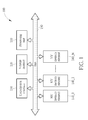
Please refer to FIG. 1 , which is a diagram illustrating a memory apparatus 100 according to a first embodiment of the present invention. The memory apparatus 100 includes a processing unit 110, a volatile memory 120, a transmission interface 130, a plurality of non-volatile (NV) memory elements 140_1, 140_2, . . . , 140_N (the symbol N represents a positive integer), and a bus 150. In typical conditions, after the transmission interface 130 is coupled to a host device (not shown in FIG. 1 ), the host device can access the memory apparatus 100 through the transmission interface 130. For example, the host device may be a personal computer such as a laptop computer or a desktop computer.
The processing unit 110 may manage the memory apparatus 100 according to program codes embedded therein or received from outside of the processing unit 110. For example, the program code may be a hardware code embedded in the processing unit 110, and more particularly, a read-only memory code (ROM code). For another example, the program code may be a firmware code received from outside of the processing unit 110. Specifically, the processing unit 110 is used to control the volatile memory 120, the transmission interface 130, the NV memory element 140_1, 140_2, . . . , 140_N and the bus 150. The processing unit 110 in this embodiment may be an advanced reduced instruction set computer machine (Advanced RISC Machine, ARM) processor or an Argonaut RISC Core (ARC) processor. However, this is merely for illustrative purpose, not a limitation to the present invention. According to a modification of this embodiment, the processing unit 110 may be other type of processor.
Further, the volatile memory 120 can be used to store a global page address linking table, the data accessed by the host device, and other information required for accessing the memory apparatus 100. In this embodiment, the volatile memory 120 may be a dynamic random access memory (DRAM). However, this is merely for illustrative purpose, not a limitation to the present invention. According to a modification of this embodiment, the volatile memory 120 may be other type of volatile memory. For example, the volatile memory 120 may include a static random access memory (SRAM).
According to this embodiment, the transmission interface 130 shown in FIG. 1 is used to transmit commands between the host device and the memory apparatus 100, wherein the transmission interface 130 meets a specific communication specification such as the serial advanced technology attachment (SATA) specification, the parallel advanced technology attachment (PATA) specification or the universal serial bus (USB) specification. For example, the memory apparatus 100 is an SSD arranged in the host device, and the specific communication specification can be one of typical communication specifications for implementing inner communications in the host device, such as the SATA and PATA specifications. For another example, the memory apparatus 100 is an SSD arranged outside of the host device, and the specific communication specification can be used to implement some typical communication specifications performed outside of the host device, such as the USB specification. However, this is merely for illustrative purpose, not a limitation to the present invention. According to a modification of this embodiment, the memory apparatus 100 can be a portable memory apparatus such as a memory card, and the specific communication can be used to implement some typical communications of the input/output (I/O) interface of a memory card, such as the secure digital (SD) specification or the compact flash (CF) specification.
Moreover, the NV memory elements 140_1, 140_2, . . . , 140_N can be used to store data, wherein the NV memory elements 140_1, 140_2, . . . , 140 N can be (but are not limited to) NAND flash chips. The bus 150 is used to couple the processing unit 110, the volatile memory 120, the transmission interface 130, and the NV memory elements 140_1, 140_2, . . . , 140_N, and used for implementing communications between these elements. In this embodiment, all elements in the structure of FIG. 1 , except the NV memory elements 140_1, 140_2, . . . , 140_N, can be integrated as a controller, especially an integrated circuit (IC) such as a controller chip. The controller is used to control at least one NV memory element in the memory apparatus 100, such as the NV memory elements 140_1, 140_2, . . . , 140_N, and can be viewed as the controller of the memory apparatus 100.
Please refer to FIG. 2 , which depicts a content arrangement of an NV memory element 140_n of the NV memory elements 140_1, 140_2, . . . , 140_N, wherein the NV memory element 140_n can be a flash chip CHP (n) in this embodiment, and the index n can represent any integer within the range [0, N]. As shown in FIG, 2, each NV memory element of the NV memory elements 140_1, 140_2, . . . , 140_N, such as the flash chip DNP(n), may include a plurality of blocks such as the blocks BLK(0), BLK (1), BLK (2), . . . , BLK (M) (the symbol M represents a positive integer), wherein each block includes a plurality of pages each including a plurality of sectors. In this embodiment, one sector can be a smallest read unit. In other words, during one read operation, the processing unit 110 may read a sector or a plurality of sectors. However, this is merely for illustrative purpose, not a limitation to the present invention.
As shown in FIG. 2 , a block (e.g. the block BLK (0)) in the NV memory element 140_n such as the flash chip CHP(n) is configured as a single level cell (SLC) memory block, and the block such as the block BLK(0) may include a predetermined number of pages, such as the pages Page (0), Page (1), Page (2), . . . , Page (63) respectively corresponding to the word-lines WL0, WL1, WL2, . . . , WL63, wherein each page such as Page (0) may include a plurality of sectors SEC (0), SEC (1), SEC (2), . . . , SEC (3). However, this is merely for illustrative purpose, not a limitation to the present invention. According to a modification of this embodiment such as the embodiment shown in FIG. 3 , under the situation that a block (e.g. the block BLK (0)) in the NV memory element 140_n (e.g. the flash chip CHP(n)) is configured as a multiple level cell (MLC) memory block (e.g. a triple level cell (TLC) memory block), the block (e.g. the block BLK(0)) may include a predetermined number of pages, such as the sets of pages {Page (0), Page (1), Page (2)}, {Page (3), Page (4), Page (5)}, {Page (6), Page (7), Page (8)}, . . . , {Page (189), Page (190), Page (191)}, wherein each page such as the page Page (0) may include sectors SEC (0), SEC (1), SEC (2) and SEC (3).
Please refer to FIG. 4 , which is a flowchart illustrating a method 200 for managing a memory apparatus according to an embodiment of the present invention. The method 200 can be applied to the memory apparatus 100 shown in FIG. 1 , especially the aforementioned controller (e.g. the memory controller that executes the aforementioned program codes through the processing unit 110), wherein the controller that executes the aforementioned program codes is used to control the aforementioned at least one NV memory element such as the NV memory elements 140_1, 140_2, . . . , 140_N shown in FIG. 1 . The method is described as follows.
In step 210, the controller temporarily stores data received from a host device into a volatile memory 120 in the controller to utilize the data in the volatile memory 120 as received data, and dynamically monitors the data amount of the received data to determine whether to immediately write the received data into the at least one NV memory element, wherein at least one write command received from the host device indicates that the host device requests to write the data. Specifically, when the amount of the received data reaches a predetermined data amount threshold PDDR_TH, the controller determines to immediately write the received data into the at least one NV memory element.
In step 220, when determining to immediately write the received data into the at least one NV memory element, the controller directly writes the received data into a specific block within a specific NV memory element of the at least one NV memory element that is configured to be an MLC memory block (e.g. the block having 192 pages Page (0), Page (1), . . . , Page (191), as shown in FIG. 3 ), rather than indirectly writes the received data into the specific block by first temporarily writing the received data into any other block configured to be an SLC memory block (e.g. the block having 64 pages Page (0), Page (1), . . . , Page (63), as shown in FIG. 2 ). For example, the NV memory element can be the flash chip CHP (n) shown in FIG. 3 , wherein the specific block can be a block of the blocks {BLK (0), BLK (1), BLK (2), . . . , BLK (M)} such as the block BLK(m), and the index m can represent any integer in the range [0, M].
According to this embodiment, under the situation that a memory cell in the specific block is used to store a plurality of bits, the plurality of bits are required to be repeatedly written into the memory cell for a predetermined number of times PDNT_WR, so as to make the memory cell in the specific NV memory element programmed correctly. In this way, each bit of the plurality of bits is correctly stored in the memory cell for further reading, wherein the predetermined number of times PDNT_WR is larger than 1. In practice, the storage capacity of the volatile memory 120 is larger than or equal to the product of the predetermined data amount threshold PDDA_TH and the predetermined number of times PDNT_WR (i.e., PDDA_TH*PDNT_WR), to allow at least a portion of the received data to be used in a repeated write operation of the memory cell. For example, regarding some types of MLC flash memories, the specific block is configured as a TLC memory block, the predetermined number of times PDNT_WR can be equal to 3, and the predetermined data amount threshold PDDA_TH can be equal to the storage capacity of a set of memory cells belonging to a word-line in the specific NV memory element. However, this is merely for illustrative purpose, not a limitation to the present invention.
Please note that, in this embodiment, the controller can directly write the received data into the specific block several times, to ensure that the user data is error-free. Specifically, under the control of the controller, the number of times the received data is written into the specific block would reach the predetermined number of times PDNT_WR, so that a specific set of memory cells belonging to a specific word-line in the specific block is correctly programmed in the NV memory element. In this way, each bit in the received data is correctly stored into the specific set of memory cells for further reading.
Further, under the situation that the host device wants to read the data from the aforementioned at least one NV memory element, the data is not yet written into any NV memory element in step 210. Hence, before determining to immediately write the received data into the aforementioned at least one NV memory element, when at least one read command received from the host device indicates that the host device requests to read at least a portion of the data, the controller can read at least the portion of the data from the volatile memory 120 to respond to the host device, instead of reading at least the portion of the data from the specific NV memory element.
According to a modification of this embodiment, the controller receives multiple sets of data {Data (0), Data (1), Data (2)}, { Data (3), Data (4), Data (5)}, {Data (6), Data (7), Data (8)}, . . . respectively, and temporally stores the sets of data {Data (0), Data (1), Data (2)}, {Data (3), Data (4), Data (5)}, {Data (6), Data (7), Data (8)}, . . . into the volatile memory 120, wherein each of the sets of data includes a plurality of pages, and the data amount of each of the sets of data is equal to the predetermined data amount threshold PDDA_TH. Specifically, the controller reads the sets of data {Data (0), Data (1), Data (2)}, {Data (3), Data (4), Data (5)}, {Data (6), Data (7), Data (8)} from the volatile memory 120, respectively, for directly writing the sets of data {Data (0), Data (1), Data (2)}, {Data (3), Data (4), Data (5)}, {Data (6), Data (7), Data (8)} into the specific block, respectively, and directly writes the first set of data {Data (0), Data (1), Data (2)} among the sets of data {Data (0), Data (1), Data (2)}, {Data (3), Data (4), Data (5)}, {Data (6), Data (7), Data (8)} into the specific block several times, wherein the number of times the first set of data {Data (0), Data (1), Data (2)} is written into the specific block would reach the predetermined number of times PDNT_WR, so that a specific set of memory cells belonging to a specific word-line in the specific block is correctly programmed in the specific NV memory element, thus making each bit of the first set of data {Data (0), Data (1), Data (2)} be correctly stored in the specific set of memory cells for further reading.
Please refer to FIGS. 5 and 6 . FIG. 5 depicts a control scheme involved by the method 200 shown in FIG. 4 in an embodiment. FIG. 6 is a flowchart illustrating the procedure 300 of the control scheme shown in FIG. 5 . In FIG. 5 , each of the sets of data Data (0), Data (1), Data (2), Data (3), Data (4), Data (5), Data (6), Data (7), Data (8), . . . can be page data. For example, the size of page data can be 16 kilobytes (KB). However, this is merely for illustrative purpose, not a limitation to the present invention.
In step 310, the controller employs a page-by-page manner to receive the first set of data {Data (0), Data (1), Data (2)} until the total data amount of the first set of data {Data (0), Data (1), Data (2)} reaches the predetermined data amount threshold PDDA_TH, and temporally stores the first set of data {Data (0), Data (1), Data (2)} in the volatile memory 120, wherein before the total data amount of the first set of data {Data (0), Data (1), Data (2)} reaches the predetermined data amount threshold PDDA_TH, the first set of data {Data (0), Data (1), Data (2)} is not written into the specific block.
In step 312, when the total data amount of the first set of data {Data (0), Data (1), Data (2)} reaches the predetermined data amount threshold PDDR_TH, the controller reads at least a portion of the first set of data {Data (0), Data (1), Data (2)} from the volatile memory 120 to directly write the first set of data {Data (0), Data (1), Data (2)} into the specific block.
In step 320, the controller employs a page-by-page manner to receive the second set of data {Data (3), Data (4), Data (5)} until the total data amount of the second set of data {Data (3), Data (4), Data (5)} reaches the predetermined data amount threshold PDDA_TH, and temporally stores the second set of data {Data (3), Data (4), Data (5)} in the volatile memory 120, wherein before the total data amount of the second set of data {Data (3), Data (4), Data (5)} reaches the predetermined data amount threshold PDDR_TH, the second set of data {Data (3), Data (4), Data (5)} is not written into the specific block.
In step 322, when the total data amount of the second set of data {Data (3), Data (4), Data (5)} reaches the predetermined data amount threshold PDDR_TH, the controller reads at least a portion of the second set of data {Data (3), Data (4), Data (5)} from the volatile memory 120 to directly write the second set of data {Data (3), Data (4), Data (5)} into the specific block, and directly writes the first set of data {Data (0), Data (1), Data (2)} into the specific block for the second time.
In step 330, the controller employs a page-by-page manner to receive the third set of data {Data (6), Data (7), Data (8)} until the total data amount of the third set of data {Data (6), Data (7), Data (8)} reaches the predetermined data amount threshold PDDA_TH, and temporally stores the third set of data {Data (6), Data (7), Data (8)} in the volatile memory 120, wherein before the total data amount of the third set of data {Data (6), Data (7), Data (8)} reaches the predetermined data amount threshold PDDA_TH, the third set of data {Data (6), Data (7), Data (8)} is not written into the specific block.
In step 332, when the total data amount of the third set of data {Data (6), Data (7), Data (8)} reaches the predetermined data amount threshold PDDR_TH, the controller reads at least a portion of the third set of data {Data (6), Data (7), Data (8)} from the volatile memory 120 to directly write the third set of data {Data (6), Data (7), Data (8)} into the specific block, directly writes the second set of data {Data (3), Data (4), Data (5)} into the specific block for the second time, and directly writes the first set of data {Data (0), Data (1), Data (2)} into the specific block for the third time, so that each bit of data of any page of the first set of data {Data (0), Data (1), Data (2)} is correctly stored into the specific block for further reading. For example, if the predetermined number of times PDNT_WR is equal to 3, the write operation of the first set of data {Data (0), Data (1), Data (2)} is completed.
Similarly, regarding the sets of data following the sets of data Data (0), Data (1), Data (2), Data (3), Data (4), Data (5), Data (6), Data (7), and Data (8), the controller can process them according to the procedure 300 shown in FIG. 6 , especially steps 330 and 332. For example, when the total data amount of a fourth set of data {Data (9), Data (10), Data (11)} in the sets of data Data (0), Data (1), Data (2), Data (3), Data (4), Data (5), Data (6), Data (7), Data (8), . . . reaches the predetermined data amount threshold PDDRC_TH, the controller reads at least a portion of the fourth set of data {Data (9), Data (10), Data (11)} from the volatile memory 120 to directly write the fourth set of data {Data (9), Data (10), Data (11)} into the specific block, directly writes the third set of data{Data (6), Data (7), Data (8)} into the specific block for the second time, and directly writes the second set of data {Data (3), Data (4), Data (5)} into the specific block for the third time, so that each bit of data of any page of the second set of data {Data (3), Data (4), Data (5)} is correctly stored into the specific block for further reading. For example, if the predetermined number of times PDNT_WR is equal to 3, the write operation of the second set of data {Data (3), Data (4), Data (5)} is completed. Therefore, by utilizing the procedure 300 shown in FIG. 6 , all data in the sets of data Data (0), Data (1), Data (2), Data (3), Data (4), Data (5), Data (6), Data (7), Data (8), . . . can be correctly stored into the specific block for further reading. The similar parts between the present and previous embodiments/modifications are omitted here for brevity.
Please refer to FIG. 7 , which depicts another control scheme involved by the method 200 shown in FIG. 4 in an embodiment, wherein each data of the sets of data Data (0), Data (1), Data (2), Data (3), Data (4), Data (5), Data (6), Data (7), Data (8), . . . can be 16 KB data, and can be divided into four 4 KB sub-data (in FIG. 7 , “4K” denotes the size of 4 KB). This embodiment can be applied to the write operation of data at random logical addresses. However, this is merely for illustrative purpose, not a limitation to the present invention.
According to this embodiment, the controller can utilize the volatile memory 120 to collect data at random logical addresses, wherein the size of one data for performing the random write operation can be 4 KB. When the size of the collected data reaches 16 KB, the controller treats the collected 16 KB data as one page data in the embodiment of FIG. 5 (e.g. data Data (0) or any of data Data (1), Data (2), Data (3), Data (4), Data (5), Data (6), Data (7), Data (8), . . .), and processes the collected 16 KB data in the same way mentioned above. The similar parts between the present and previous embodiments/modifications are omitted here for brevity.
Those skilled in the art will readily observe that numerous modifications and alterations of the device and method may be made while retaining the teachings of the invention. Accordingly, the above disclosure should be construed as limited only by the metes and bounds of the appended claims.
Claims (20)
1. A method for managing a memory apparatus, the memory apparatus comprising at least one non-volatile (NV) memory element, each of the at least one NV memory element comprising a plurality of blocks, the method applied to a controller of the memory apparatus, the controller being used to control the at least one NV element, the method comprising following steps:
temporarily storing data received from a host device into a volatile memory in the controller and utilizing the data in the volatile memory as received data, and dynamically monitoring a data amount of the received data to determine whether to immediately write the received data into the at least one NV memory element, wherein at least one write command received from the host device indicates that the host device requests to write the data; and
when determining to immediately write the received data into the at least one NV memory element, directly writing the received data into a specific block configured to be a Multiple Level Cell (MLC) memory block within a specific NV memory element of the at least one NV memory element, rather than indirectly writing the received data into the specific block by first temporarily writing the received data into any other block configured to be a Single Level Cell (SLC) memory block.
2. The method of claim 1 , wherein under a situation that a memory cell in the specific block is used to store a plurality of bits, the plurality of bits need to be repeatedly written into the memory cell for a predetermined number of times, so that the memory cell is correctly programmed in the specific NV memory element, thus making each of the plurality of bits correctly stored into the memory cell for further reading; and the predetermined number of times is larger than 1.
3. The method of claim 2 , wherein the step of dynamically monitoring the data amount of the received data comprises:
when the data amount of the received data reaches a predetermined data amount threshold, determining to immediately write the received data into the at least one NV memory element;
wherein a storage capacity of the volatile memory is larger than or equal to a product of the predetermined data amount threshold and the predetermined number of times, to allow at least a portion of the received data to be used in a repeated write operation of the memory cell.
4. The method of claim 3 , wherein the predetermined data amount threshold is equal to a storage capacity of a set of memory cells belonging to a word-line in the specific NV memory element.
5. The method of claim 4 , wherein any of the plurality of blocks comprises a predetermined number of pages; and the method further comprises:
receiving a plurality of sets of data from the host device, respectively, and temporarily storing the plurality of sets of data into the volatile memory, wherein each of the plurality of sets of data comprises a plurality of pages, and a data amount of each of the plurality of sets of data is equal to the predetermined data amount threshold; and
reading the plurality of sets of data from the volatile memory, to directly write the plurality of sets of data into the specific block, respectively, and directly writing a first set of data of the plurality of sets of data into the specific block several times, wherein a number of times the first set of data is written into the specific block reaches the predetermined number of times, so that a specific set of memory cells belonging to a specific word-line in the specific block is correctly programmed in the specific NV memory element, thus making each bit of the first set of data correctly stored in the specific set of memory cells for further reading.
6. The method of claim 2 , wherein any of the plurality of blocks comprises a predetermined number of pages; and the method further comprises:
respectively receiving a first set of data comprising a plurality of pages from the host device in a page-by-page manner until a total received data amount of the first set of data reaches a predetermined data amount threshold, and temporally storing the first set of data into the volatile memory, wherein before the total received data amount of the first set of data reaches the predetermined data amount threshold, the first set of data is not written into the specific block; and
when the total received data amount of the first set of data reaches the predetermined data amount threshold, reading at least a portion of the first set of data from the volatile memory to directly write the first set of data into the specific block.
7. The method of claim 6 , further comprising:
respectively receiving a second set of data comprising a plurality of pages from the host device in a page-by-page manner until a total received data amount of the second set of data reaches the predetermined data amount threshold, and temporally storing the second set of data into the volatile memory, wherein before the total received data amount of the second set of data reaches the predetermined data amount threshold, the second set of data is not written into the specific block; and
when the total received data amount of the second set of data reaches the predetermined data amount threshold, reading at least a portion of the second set of data from the volatile memory to directly write the second set of data into the specific block, and directly writing the first set of data into the specific block for a second time.
8. The method of claim 7 , further comprising:
respectively receiving a third set of data comprising a plurality of pages from the host device in a page-by-page manner until a total received data amount of the third set of data reaches the predetermined data amount threshold, and temporally storing the third set of data into the volatile memory, wherein before the total received data amount of the third set of data reaches the predetermined data amount threshold, the third set of data is not written into the specific block; and
when the total received data amount of the third set of data reaches the predetermined data amount threshold, reading at least a portion of the third set of data from the volatile memory to directly write the third set of data into the specific block, directly writing the second set of data into the specific block for a second time, and directly writing the first set of data into the specific block for a third time, so that each bit of data of any page of the first set of data is correctly stored into the specific block for further reading.
9. The method of claim 1 , further comprising:
before determining to immediately write the received data into the at least one NV memory element:
when at least one read command received from the host device indicates that the host device requests to read at least a portion of the data, reading at least the portion of the data from the volatile memory to respond to the host device, instead of reading at least the portion of the data from the specific NV memory element.
10. The method of claim 1 , further comprising:
directly writing the received data into the specific block several times, wherein under control of the controller, a number of times the received data is written into the specific block reaches a predetermined number of times, so that a specific set of memory cells belonging to a specific word-line in the specific block is correctly programmed in the NV memory element, thus making each bit in the received data correctly stored into the specific set of memory cells for further reading.
11. A memory apparatus, comprising:
at least one non-volatile (NV) memory element, each comprising
a plurality of blocks; and
a controller, arranged to control the at least one NV element, the controller comprising a processing unit arranged to manage the memory apparatus according to a program code embedded in the processing unit or received from outside of the processing unit, wherein the controller temporarily stores data received from a host device into a volatile memory in the controller and utilizes the data in the volatile memory as received data, and dynamically monitors a data amount of the received data to determine whether to immediately write the received data into the at least one NV memory element, wherein at least one write command received from the host device indicates that the host device requests to write the data;
wherein when determining to immediately write the received data into the at least one NV memory element, the controller directly writes the received data into a specific block configured to be a Multiple Level Cell (MLC) memory block within a specific NV memory element of the at least one NV memory element, rather than indirectly writes the received data into the specific block by first temporarily writing the received data into any other block configured to be a Single Level Cell (SLC) memory block.
12. The memory apparatus of claim 11 , wherein under a situation that a memory cell in the specific block is used to store a plurality of bits, the plurality of bits need to be repeatedly written into the memory cell for a predetermined number of times, so that the memory cell is correctly programmed in the specific NV memory element, thus making each of the plurality of bits correctly stored into the memory cell for further reading; and the predetermined number of times is larger than 1.
13. The memory apparatus of claim 12 , wherein when the data amount of the received data reaches a predetermined data amount threshold, the controller determines to immediately write the received data into the at least one NV memory element; and a storage capacity of the volatile memory is not less than a product of the predetermined data amount threshold and the predetermined number of times to allow at least a portion of the received data to be used in a repeated write operation of the memory cell.
14. The memory apparatus of claim 13 , wherein the predetermined data amount threshold is equal to a storage capacity of a set of memory cells belonging to a word-line in the specific NV memory element.
15. The memory apparatus of claim 14 , wherein any of the plurality of blocks comprises a predetermined number of pages; the controller receives a plurality of sets of data from the host device, respectively, and temporarily stores the plurality of sets of data into the volatile memory, wherein each of the plurality of sets of data comprises a plurality of pages, and a data amount of each of the plurality of sets of data is equal to the predetermined data amount threshold; and the controller reads the plurality of sets of data from the volatile memory to directly write the plurality of sets of data into the specific block, respectively, and directly writes a first set of data of the plurality of sets of data into the specific block several times, wherein a number of times the first set of data is written into the specific block reaches the predetermined number of times, so that a specific set of memory cells belonging to a specific word-line in the specific block is correctly programmed in the specific NV memory element, thus making each bit of the first set of data correctly stored in the specific set of memory cells for further reading.
16. A controller of a memory apparatus, the memory apparatus comprising at least one non-volatile (NV) memory element each comprising a plurality of blocks, the controller comprising:
a processing unit, arranged to manage the memory apparatus according to a program code embedded in the processing unit or received from outside of the processing unit, wherein the controller temporarily stores data received from a host device into a volatile memory in the controller and utilizes the data in the volatile memory as received data, and dynamically monitors a data amount of the received data to determine whether to immediately write the received data into the at least one NV memory element, wherein at least one write command received from the host device indicates that the host device requests to write the data; and
wherein when determining to immediately write the received data into the at least one NV memory element, the controller directly writes the received data into a specific block configured to be a Multiple Level Cell (MLC) memory block within a specific NV memory element of the at least one NV memory element, rather than indirectly writes the received data into the specific block by first temporarily writing the received data into any other block configured to be a Single Level Cell (SLC) memory block.
17. The controller of claim 16 , wherein under a situation that a memory cell in the specific block is used to store a plurality of bits, the plurality of bits need to be repeatedly written into the memory cell for a predetermined number of times, so that the memory cell is correctly programmed in the specific NV memory element, thus making each of the plurality of bits correctly stored into the memory cell for further reading; and the predetermined number of times is larger than 1.
18. The controller of claim 17 , wherein when the data amount of the received data reaches a predetermined data amount threshold, the controller determines to immediately write the received data into the at least one NV memory element; and a storage capacity of the volatile memory is larger than or equal to a product of the predetermined data amount threshold and the predetermined number of times to allow at least a portion of the received data to be used in a repeated write operation of the memory cell.
19. The controller of claim 18 , wherein the predetermined data amount threshold is equal to a capacity of a set of memory cells belonging to a word-line in the specific NV memory element.
20. The controller of claim 19 , wherein any of the plurality of blocks comprises a predetermined number of pages; the controller receives a plurality of sets of data from the host device, respectively, and temporarily stores the plurality of sets of data into the volatile memory, wherein each of the plurality of sets of data comprises a plurality of pages, and a data amount of each of the plurality of sets of data is equal to the predetermined data amount threshold; and the controller reads the plurality of sets of data from the volatile memory to directly write the plurality of sets of data into the specific block, respectively, and directly writes a first set of data of the plurality of sets of data into the specific block several times, wherein a number of times the first set of data is written into the specific block reaches the predetermined number of times, so that a specific set of memory cells belonging to a specific word-line in the specific block is correctly programmed in the specific NV memory element, thus making each bit of the first set of data correctly stored in the specific set of memory cell for further reading.
Priority Applications (1)
| Application Number | Priority Date | Filing Date | Title |
|---|---|---|---|
| US14/334,684 US9514042B2 (en) | 2013-08-05 | 2014-07-18 | Method for managing memory apparatus to perform writing control according to monitored data amount of received data, associated memory apparatus thereof and associated controller thereof |
Applications Claiming Priority (5)
| Application Number | Priority Date | Filing Date | Title |
|---|---|---|---|
| US201361862094P | 2013-08-05 | 2013-08-05 | |
| TW102144913A TWI523016B (en) | 2013-08-05 | 2013-12-06 | Method for managing a memory apparatus, and associated memory apparatus thereof and associated controller thereof |
| TW102144913A | 2013-12-06 | ||
| TW102144913 | 2013-12-06 | ||
| US14/334,684 US9514042B2 (en) | 2013-08-05 | 2014-07-18 | Method for managing memory apparatus to perform writing control according to monitored data amount of received data, associated memory apparatus thereof and associated controller thereof |
Publications (2)
| Publication Number | Publication Date |
|---|---|
| US20150039810A1 US20150039810A1 (en) | 2015-02-05 |
| US9514042B2 true US9514042B2 (en) | 2016-12-06 |
Family
ID=52428745
Family Applications (1)
| Application Number | Title | Priority Date | Filing Date |
|---|---|---|---|
| US14/334,684 Active 2035-01-05 US9514042B2 (en) | 2013-08-05 | 2014-07-18 | Method for managing memory apparatus to perform writing control according to monitored data amount of received data, associated memory apparatus thereof and associated controller thereof |
Country Status (3)
| Country | Link |
|---|---|
| US (1) | US9514042B2 (en) |
| KR (1) | KR101561546B1 (en) |
| CN (3) | CN107423231B (en) |
Cited By (2)
| Publication number | Priority date | Publication date | Assignee | Title |
|---|---|---|---|---|
| US10152252B2 (en) | 2016-04-27 | 2018-12-11 | SK Hynic Inc. | Memory system and operating method thereof |
| TWI739440B (en) * | 2020-02-19 | 2021-09-11 | 慧榮科技股份有限公司 | Method for performing data storage management to enhance data reliability, associated memory device and controller thereof, and associated electronic device |
Families Citing this family (7)
| Publication number | Priority date | Publication date | Assignee | Title |
|---|---|---|---|---|
| CN107423231B (en) * | 2013-08-05 | 2020-11-20 | 慧荣科技股份有限公司 | Method for managing a memory device, memory device and controller |
| US9928169B2 (en) * | 2014-05-07 | 2018-03-27 | Sandisk Technologies Llc | Method and system for improving swap performance |
| CN107544922B (en) * | 2016-06-24 | 2020-01-21 | 群联电子股份有限公司 | Data writing method, memory control circuit unit and memory storage device |
| TWI640867B (en) * | 2017-05-02 | 2018-11-11 | 慧榮科技股份有限公司 | Data storage device and operating method therefor |
| KR20190074677A (en) | 2017-12-20 | 2019-06-28 | 에스케이하이닉스 주식회사 | Memory system and operating method of memory system |
| KR20200015247A (en) | 2018-08-03 | 2020-02-12 | 에스케이하이닉스 주식회사 | Memory system and operating method thereof |
| US11526619B2 (en) * | 2019-06-28 | 2022-12-13 | Bank Of America Corporation | System for securing and allowing access to electronic data in a data storage container |
Citations (15)
| Publication number | Priority date | Publication date | Assignee | Title |
|---|---|---|---|---|
| KR20080091203A (en) | 2006-01-18 | 2008-10-09 | 트렉 2000 인터네셔널 엘티디. | Portable data storage device incorporating multiple flash memory units |
| US20090300269A1 (en) * | 2008-05-28 | 2009-12-03 | Radke William H | Hybrid memory management |
| US20100023682A1 (en) | 2007-10-11 | 2010-01-28 | Super Talent Electronics Inc. | Flash-Memory System with Enhanced Smart-Storage Switch and Packed Meta-Data Cache for Mitigating Write Amplification by Delaying and Merging Writes until a Host Read |
| US20100042773A1 (en) | 2008-08-12 | 2010-02-18 | Phison Electronics Corp. | Flash memory storage system and data writing method thereof |
| US20100115192A1 (en) | 2008-11-05 | 2010-05-06 | Samsung Electronics Co., Ltd. | Wear leveling method for non-volatile memory device having single and multi level memory cell blocks |
| US20100174847A1 (en) | 2009-01-05 | 2010-07-08 | Alexander Paley | Non-Volatile Memory and Method With Write Cache Partition Management Methods |
| TW201030521A (en) | 2009-02-10 | 2010-08-16 | Phison Electronics Corp | Multi level cell NAND flash memory storage system, and controller and accessing method thereof |
| TW201035757A (en) | 2009-03-20 | 2010-10-01 | Phison Electronics Corp | Data storing method for a flash memory and storage system |
| JP2010250846A (en) | 2007-12-28 | 2010-11-04 | Toshiba Corp | Semiconductor storage device |
| US20110041005A1 (en) | 2009-08-11 | 2011-02-17 | Selinger Robert D | Controller and Method for Providing Read Status and Spare Block Management Information in a Flash Memory System |
| US8040744B2 (en) | 2009-01-05 | 2011-10-18 | Sandisk Technologies Inc. | Spare block management of non-volatile memories |
| US20120246391A1 (en) | 2011-01-27 | 2012-09-27 | Anobit Technologies | Block management schemes in hybrid slc/mlc memory |
| US20120254574A1 (en) | 2011-03-31 | 2012-10-04 | Alan Welsh Sinclair | Multi-layer memory system |
| KR20130010447A (en) | 2011-07-18 | 2013-01-28 | 애플 인크. | Non-volatile temporary data handling |
| US20130173844A1 (en) | 2011-12-29 | 2013-07-04 | Jian Chen | SLC-MLC Wear Balancing |
Family Cites Families (4)
| Publication number | Priority date | Publication date | Assignee | Title |
|---|---|---|---|---|
| CN101526883B (en) * | 2008-03-03 | 2011-10-19 | 群联电子股份有限公司 | Data stream transmission and dispatch method, system for executing same and controller of the system |
| CN101576853B (en) * | 2008-05-06 | 2011-12-21 | 群联电子股份有限公司 | Data access method and controller and memory system using same |
| CN102541675B (en) * | 2010-12-23 | 2015-03-11 | 慧荣科技股份有限公司 | Method for improving error correction capacity, memorization device and controller for memorization device |
| CN107423231B (en) * | 2013-08-05 | 2020-11-20 | 慧荣科技股份有限公司 | Method for managing a memory device, memory device and controller |
-
2014
- 2014-06-18 CN CN201710518261.6A patent/CN107423231B/en active Active
- 2014-06-18 CN CN201710380118.5A patent/CN107391389B/en active Active
- 2014-06-18 CN CN201410272738.3A patent/CN104346288B/en active Active
- 2014-07-18 US US14/334,684 patent/US9514042B2/en active Active
- 2014-08-05 KR KR1020140100426A patent/KR101561546B1/en active IP Right Grant
Patent Citations (18)
| Publication number | Priority date | Publication date | Assignee | Title |
|---|---|---|---|---|
| KR20080091203A (en) | 2006-01-18 | 2008-10-09 | 트렉 2000 인터네셔널 엘티디. | Portable data storage device incorporating multiple flash memory units |
| US7962685B2 (en) | 2006-01-18 | 2011-06-14 | Trek 2000 International Ltd. | Portable data storage device incorporating multiple flash memory units |
| US20100023682A1 (en) | 2007-10-11 | 2010-01-28 | Super Talent Electronics Inc. | Flash-Memory System with Enhanced Smart-Storage Switch and Packed Meta-Data Cache for Mitigating Write Amplification by Delaying and Merging Writes until a Host Read |
| JP2010250846A (en) | 2007-12-28 | 2010-11-04 | Toshiba Corp | Semiconductor storage device |
| US9134924B2 (en) | 2007-12-28 | 2015-09-15 | Kabushiki Kaisha Toshiba | Semiconductor storage device with volatile and nonvolatile memories to allocate blocks to a memory and release allocated blocks |
| US20120311245A1 (en) | 2007-12-28 | 2012-12-06 | Hirokuni Yano | Semiconductor storage device with volatile and nonvolatile memories |
| US20090300269A1 (en) * | 2008-05-28 | 2009-12-03 | Radke William H | Hybrid memory management |
| US20100042773A1 (en) | 2008-08-12 | 2010-02-18 | Phison Electronics Corp. | Flash memory storage system and data writing method thereof |
| US20100115192A1 (en) | 2008-11-05 | 2010-05-06 | Samsung Electronics Co., Ltd. | Wear leveling method for non-volatile memory device having single and multi level memory cell blocks |
| US8040744B2 (en) | 2009-01-05 | 2011-10-18 | Sandisk Technologies Inc. | Spare block management of non-volatile memories |
| US20100174847A1 (en) | 2009-01-05 | 2010-07-08 | Alexander Paley | Non-Volatile Memory and Method With Write Cache Partition Management Methods |
| TW201030521A (en) | 2009-02-10 | 2010-08-16 | Phison Electronics Corp | Multi level cell NAND flash memory storage system, and controller and accessing method thereof |
| TW201035757A (en) | 2009-03-20 | 2010-10-01 | Phison Electronics Corp | Data storing method for a flash memory and storage system |
| US20110041005A1 (en) | 2009-08-11 | 2011-02-17 | Selinger Robert D | Controller and Method for Providing Read Status and Spare Block Management Information in a Flash Memory System |
| US20120246391A1 (en) | 2011-01-27 | 2012-09-27 | Anobit Technologies | Block management schemes in hybrid slc/mlc memory |
| US20120254574A1 (en) | 2011-03-31 | 2012-10-04 | Alan Welsh Sinclair | Multi-layer memory system |
| KR20130010447A (en) | 2011-07-18 | 2013-01-28 | 애플 인크. | Non-volatile temporary data handling |
| US20130173844A1 (en) | 2011-12-29 | 2013-07-04 | Jian Chen | SLC-MLC Wear Balancing |
Cited By (3)
| Publication number | Priority date | Publication date | Assignee | Title |
|---|---|---|---|---|
| US10152252B2 (en) | 2016-04-27 | 2018-12-11 | SK Hynic Inc. | Memory system and operating method thereof |
| TWI739440B (en) * | 2020-02-19 | 2021-09-11 | 慧榮科技股份有限公司 | Method for performing data storage management to enhance data reliability, associated memory device and controller thereof, and associated electronic device |
| TWI782644B (en) * | 2020-02-19 | 2022-11-01 | 慧榮科技股份有限公司 | Method for performing data storage management to enhance data reliability, associated memory device and controller thereof, and associated electronic device |
Also Published As
| Publication number | Publication date |
|---|---|
| CN107391389B (en) | 2020-11-24 |
| US20150039810A1 (en) | 2015-02-05 |
| CN104346288A (en) | 2015-02-11 |
| CN107423231B (en) | 2020-11-20 |
| KR20150016914A (en) | 2015-02-13 |
| CN107423231A (en) | 2017-12-01 |
| CN107391389A (en) | 2017-11-24 |
| KR101561546B1 (en) | 2015-10-19 |
| CN104346288B (en) | 2017-07-28 |
Similar Documents
| Publication | Publication Date | Title |
|---|---|---|
| US9514042B2 (en) | Method for managing memory apparatus to perform writing control according to monitored data amount of received data, associated memory apparatus thereof and associated controller thereof | |
| US9570183B1 (en) | Method and controller for managing memory device | |
| US9507708B2 (en) | Method for managing memory apparatus, associated memory apparatus thereof and associated controller thereof | |
| US10102059B2 (en) | Data storage device capable of preventing a data retention fail of a nonvolatile memory device and operating method thereof | |
| US11630768B2 (en) | Method for managing flash memory module and associated flash memory controller and electronic device | |
| US11282564B1 (en) | Selective wordline scans based on a data state metric | |
| US9141530B2 (en) | Data writing method, memory controller and memory storage device | |
| US9524791B1 (en) | Data storage device and operating method thereof | |
| KR20170026831A (en) | Nonvolatile memory device, data storage device including thereof and operating method for data storage device | |
| US20140013030A1 (en) | Memory storage device, memory controller thereof, and method for writing data thereof | |
| US9123443B2 (en) | Memory device, memory management device, and memory management method | |
| CN111158579A (en) | Solid state disk and data access method thereof | |
| CN115240745A (en) | Storing high read data at low impact read disturb pages of a memory device | |
| KR20130087936A (en) | Memory device, memory system and program method of the same | |
| US9728264B2 (en) | Nonvolatile memory device, operating method thereof, and data storage device including the same | |
| CN114968079A (en) | Electronic system including memory system and host | |
| US8713242B2 (en) | Control method and allocation structure for flash memory device | |
| TWI523016B (en) | Method for managing a memory apparatus, and associated memory apparatus thereof and associated controller thereof | |
| US20230031193A1 (en) | Memory system and operating method thereof | |
| CN110322913B (en) | Memory management method and memory controller | |
| US10726938B2 (en) | Data storage device and operating method thereof |
Legal Events
| Date | Code | Title | Description |
|---|---|---|---|
| AS | Assignment |
Owner name: SILICON MOTION INC., TAIWAN Free format text: ASSIGNMENT OF ASSIGNORS INTEREST;ASSIGNORS:CHOU, PO-SHENG;FAN, YU-WEI;CHAN, CHUNG-YUAN;REEL/FRAME:033339/0011 Effective date: 20140716 |
|
| STCF | Information on status: patent grant |
Free format text: PATENTED CASE |
|
| MAFP | Maintenance fee payment |
Free format text: PAYMENT OF MAINTENANCE FEE, 4TH YEAR, LARGE ENTITY (ORIGINAL EVENT CODE: M1551); ENTITY STATUS OF PATENT OWNER: LARGE ENTITY Year of fee payment: 4 |