US9509305B2 - Power gating techniques with smooth transition - Google Patents
Power gating techniques with smooth transition Download PDFInfo
- Publication number
- US9509305B2 US9509305B2 US14/151,337 US201414151337A US9509305B2 US 9509305 B2 US9509305 B2 US 9509305B2 US 201414151337 A US201414151337 A US 201414151337A US 9509305 B2 US9509305 B2 US 9509305B2
- Authority
- US
- United States
- Prior art keywords
- current
- transistor
- amount
- voltage regulator
- regulator
- Prior art date
- Legal status (The legal status is an assumption and is not a legal conclusion. Google has not performed a legal analysis and makes no representation as to the accuracy of the status listed.)
- Active, expires
Links
- 230000007704 transition Effects 0.000 title claims abstract description 47
- 238000000034 method Methods 0.000 title claims abstract description 32
- 230000008859 change Effects 0.000 claims abstract description 9
- 230000007423 decrease Effects 0.000 claims description 10
- 230000003247 decreasing effect Effects 0.000 claims description 6
- 230000004044 response Effects 0.000 claims description 5
- 239000008186 active pharmaceutical agent Substances 0.000 description 15
- 238000010586 diagram Methods 0.000 description 8
- 230000015654 memory Effects 0.000 description 4
- 238000013459 approach Methods 0.000 description 2
- 230000008901 benefit Effects 0.000 description 2
- 239000003990 capacitor Substances 0.000 description 2
- 230000000694 effects Effects 0.000 description 2
- 238000005516 engineering process Methods 0.000 description 2
- 230000006870 function Effects 0.000 description 2
- 238000004377 microelectronic Methods 0.000 description 2
- 238000012986 modification Methods 0.000 description 2
- 230000004048 modification Effects 0.000 description 2
- 230000003068 static effect Effects 0.000 description 2
- AAHNBILIYONQLX-UHFFFAOYSA-N 6-fluoro-3-[4-[3-methoxy-4-(4-methylimidazol-1-yl)phenyl]triazol-1-yl]-1-(2,2,2-trifluoroethyl)-4,5-dihydro-3h-1-benzazepin-2-one Chemical compound COC1=CC(C=2N=NN(C=2)C2C(N(CC(F)(F)F)C3=CC=CC(F)=C3CC2)=O)=CC=C1N1C=NC(C)=C1 AAHNBILIYONQLX-UHFFFAOYSA-N 0.000 description 1
- 101100449736 Candida albicans (strain SC5314 / ATCC MYA-2876) ZCF23 gene Proteins 0.000 description 1
- 101150016162 GSM1 gene Proteins 0.000 description 1
- 230000033228 biological regulation Effects 0.000 description 1
- 238000013461 design Methods 0.000 description 1
- 229920005994 diacetyl cellulose Polymers 0.000 description 1
- 238000003384 imaging method Methods 0.000 description 1
- 238000007689 inspection Methods 0.000 description 1
- 238000004806 packaging method and process Methods 0.000 description 1
- 238000012536 packaging technology Methods 0.000 description 1
- 229920000729 poly(L-lysine) polymer Polymers 0.000 description 1
- 238000012913 prioritisation Methods 0.000 description 1
- 230000008569 process Effects 0.000 description 1
- 238000012545 processing Methods 0.000 description 1
- 239000004065 semiconductor Substances 0.000 description 1
- 230000001360 synchronised effect Effects 0.000 description 1
- 230000002123 temporal effect Effects 0.000 description 1
- 230000001225 therapeutic effect Effects 0.000 description 1
Images


Classifications
-
- H—ELECTRICITY
- H03—ELECTRONIC CIRCUITRY
- H03K—PULSE TECHNIQUE
- H03K19/00—Logic circuits, i.e. having at least two inputs acting on one output; Inverting circuits
- H03K19/0008—Arrangements for reducing power consumption
- H03K19/0013—Arrangements for reducing power consumption in field effect transistor circuits
Definitions
- This disclosure relates generally to electronic circuits and devices, and more specifically, to systems and methods for enabling power gating techniques with smooth transition.
- Techniques for managing the power consumption of electronic devices may include the use of Integrated Circuits (ICs) having multiple power domains.
- ICs Integrated Circuits
- each power domain may allow a circuit block within the IC to use a different amount of power than other circuit blocks.
- the use of power domains may enable one or more circuit blocks to receive different amounts of power depending upon the device's mode of operation, which can change over time.
- different power domains may be separated by one or more power switches or the like. For example, when a circuit block within a given power domain is turned on, a corresponding switch may allow that circuit to draw electrical current from a power source. These techniques are often referred to as “power gating.”
- FIG. 1 is a block diagram of an example of an electronic device according to some embodiments.
- FIG. 2 is a circuit diagram of an example of a power switch with current limitation according to some embodiments.
- FIG. 3 shows graphs illustrating aspects of the operation of a power switch with current limitation according to some embodiments.
- FIG. 4 is a circuit diagram of an example of a power switch with current limitation and zero Direct Current (DC) power consumption according to some embodiments.
- FIG. 5 is a flowchart of a method for enabling power gating techniques with smooth transition according to some embodiments.
- FIG. 6 shows graphs illustrating methods for enabling power gating techniques with smooth transition according to some embodiments.
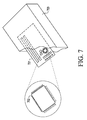
- FIG. 7 is a diagram of an example of an electronic system having one or more electronic microelectronic device packages, according to some embodiments.
- first regulator 101 and second regulator 102 are coupled to integrated circuit 104 having two or more power domains (PDs) 111 and 112 , respectively.
- First regulator 101 and second regulator 102 are also coupled to switching circuit 103 .
- second regulator 102 , switching circuit 103 , and integrated circuit 104 may all be within the same electronic package, and first voltage regulator 101 may be external to that electronic package.
- first regulator 101 may be a high power voltage regulator and second regulator 102 may be a low power (or ultra-low power) voltage regulator.
- first regulator 101 is shown as receiving V SUPPLY at transistor 105 and outputting V DD at an output node between transistor 105 and capacitor 106 , which in turn is coupled to a reference node (GND).
- second regulator 102 receives V SUPPLY at transistor 107 and outputs V DDO at an output node between transistor 107 and capacitor 108 , which in turn is coupled to GND.
- each of regulators 101 and 102 may include a number of other internal electronic components in addition to and/or as an alternative to those shown herein.
- each of regulators 101 and 102 may be a different type of voltage regulator including, but not limited to, linear regulators, switching regulators, etc.
- switching circuit 103 operates to separate the various power domains 111 and 112 . Even when power domains 111 and 112 are configured to operate based on the same supply voltage, they may each be configured to draw up to a maximum amount of current from regulators 101 and/or 102 . For example, power domain 111 may be configured to use up to 500 mA and power domain 112 may be configured to use up to 50 mA.
- switching circuit 103 may be configured to limit an amount of current drawn by a given one of power domains 111 and 112 from regulators 101 and/or 102 during a transition period—e.g., during a switching between (i) a high power mode where V DD is provided by first regulator 101 and second regulator 102 is turned off, and (ii) a low power mode where V DDO is provided by second regulator 102 and first regulator 101 is turned off.
- both the first and second regulators 101 and 102 may be turned on.
- switching circuit 103 may be configured to consume zero Direct Current (DC) power, also known as static power, be it closed or open (excluding consumption due to leakage effects or the like).
- DC Direct Current
- first regulator 101 may output a voltage V DD slightly higher than voltage V DDO that would otherwise be output by second regulator 102 , and therefore second regulator 102 may be turned off.
- first and second regulators 101 and 102 have the same nominal output voltage (e.g., 1.2 V)
- certain variations may still cause them to output slightly different voltages (e.g., 1.21 and 1.18 V).
- a determination may be made that device 100 begin operating in a low power mode.
- switch 109 within switching circuit 103 may be in a closed state—i.e., fully conductive—and, at the end of the transition period, switch 109 may be in an open state—i.e., fully non-conductive.
- current limitation element 110 of switching circuit 103 may operate to control an amount of current that is allowed to flow from first regulator 101 to second regulator 102 , and therefore it may also control an amount of current that can be drawn by a given one of power domains 111 and/or 112 from the first and/or second regulators 101 and 102 .
- the current limitation provided by switching circuit 103 may impose gradually increasing limits upon that amount of current, which then promotes a smooth transition between the two operating modes (e.g., from a high power mode to a low power mode), as described in more detail below.
- power domains 111 and 112 may represent different areas of integrated circuit 104 responsible for performing different operations.
- each of power domains 111 and 112 may include analog circuits, digital memories, processors, etc.
- device 100 is shown for sake of illustration only. In various embodiments, any number of power supplies, switches, and/or power domains may be used, and these elements may be coupled to one another in any suitable manner.
- FIG. 2 is a circuit diagram of an example of switching circuit 103 with current limitation according to some embodiments.
- switching circuit 103 is shown coupled between first regulator 101 and second regulator 102 , as originally discussed in FIG. 1 . It will be understood, however, that switching circuit 103 may be used in other contexts as well.
- switching circuit 103 includes first P-type Metal-Oxide-Semiconductor (PMOS) transistor M 1 having its source terminal (more generally referred to as a first current terminal or electrode) coupled to first regulator 101 , thus receiving supply voltage V DD , and its drain terminal (more generally referred to as a second current terminal or electrode) coupled to power domain 105 B, thus providing V DDO (where V DDO is equal to V DD minus the voltage drop across M 1 ).
- Second PMOS transistor M 2 has its source terminal coupled to first regulator 101 , thus also receiving supply voltage V DD , and its gate (more generally referred to as a control terminal or electrode) coupled to the gate of first PMOS transistor M 1 .
- transistors M 1 and M 2 form first current mirror 201 .
- M 1 operates as a current limitation transistor
- M 2 operates as a main switching transistor.
- Switch 103 also includes third PMOS transistor M 3 having its source terminal coupled to the drain terminal of second PMOS transistor M 2 , and its drain terminal coupled to node n 1 and to the gates of the first and second PMOS transistors M 1 and M 2 , respectively.
- Fourth PMOS transistor M 4 has its source terminal coupled to the drain terminal of first PMOS transistor M 1 , its drain terminal coupled to node n 0 , and its gate terminal coupled to the gate terminal of third PMOS transistor M 3 and to node n 0 .
- transistors M 3 and M 4 form second current mirror 202 .
- Current source I 10 is coupled between node n 1 and a reference node (GND) 106
- current source I 11 is coupled between node n 0 and the reference node 106 .
- Current sources I 10 and I 11 may be implemented using well-known components.
- Nodes n 0 , n 1 , and n 3 are shown such that node n 1 is the node between the gate terminals of transistors M 1 and M 2 , the drain terminal of transistor M 3 , and current source I 10 .
- Node n 0 is the node between the gate terminals of transistors M 3 and M 4 , the drain terminal of transistor M 4 , and current source I 11 .
- Node n 3 is the node between the drain of transistor M 2 and the source of transistor M 3 .
- switching circuit 103 allows only a limited amount of electrical current I LIM to flow through it.
- I LIM is a function of the current at the drain terminals of transistors M 3 and M 4 , designated as I 1 , as well as of the aspect ratios of transistors M 1 and M 2 .
- transistors M 3 and M 4 let us define:
- K 34 W 3 / L 3 W 4 / L 4
- W n is the width and L n is the length of the channel formed in transistor M n such that W 3 /L 3 is the aspect ratio of transistor M 3 and W 4 /L 4 is the aspect ratio of transistor M 4 .
- transistors M 3 and M 4 may be unbalanced such that W 4 /L 4 is greater than W 3 /L 3 .
- the gate-to-source voltage of transistor M 3 (V GS3 ) is greater than the gate-to-source voltage of transistor M 4 (V GS4 ), such that K 34 ⁇ 1.
- the current equations for transistors M 3 and M 4 in saturation are:
- I Dn is the drain current of transistor M n . If we use V T as the threshold voltage and K p as the transconductance parameter for transistor M 3 , then:
- V GS ⁇ ⁇ 4 V T + I 1 K P 2 ⁇ W 4 L 4
- V GS drop voltages in saturation region, considering the same I 1 current pass by M 3 and M 4 is calculated.
- ⁇ V GS34 is then calculated as:
- V GS3 ⁇ V GS4 transistor M 3 allows I 1 current to pass, and, therefore, V DSM3 will be low (whether transistor M 3 is in saturation, triode or linear regions). Conversely, if V GS3 is not higher than V GS4 by at least ⁇ V GS34 , then transistor M 3 just allow a current lower than I 1 to pass, and V DS3 increases.
- V DD ⁇ V DDO >V DD ⁇ V ( n 1) ⁇ V T and V DD ⁇ V ( n 3)> V DD ⁇ V ( n 1) ⁇ V T
- I L ⁇ ⁇ IM I 1 ⁇ W 1 / L 1 W 2 / L 2 Eq . ⁇ 1
- V GS ⁇ ⁇ 2 - V T 1 V DS ⁇ ⁇ 2 ⁇ ⁇ I 1 K P ⁇ W 2 / L 2 + V DS ⁇ ⁇ 2 2 2 ⁇
- V DS2 has the ⁇ V GS34 term when compared to V DS1 . This way V DS2 will decrease more than V DS1 .
- V GS2 is inversely proportional to V DS2 , the net effect is that while V DDO approaches to V DD value, V DS1 decreases, V DS2 decreases more and V GS2 increases making I LIM also increase.
- V DDO approaches V DD
- V DS1 V DD ⁇ V DDO
- I LIM decreases.
- transistors M 1 and M 2 act as a current mirror.
- the value of V DD is close to V DDO and M 2 is in triode, the value of the current limitation provided by transistor M 1 rises because (W 4 /L 4 )>(W 3 /L 3 ).
- V DD has approximately the same value as V DDO and M 2 is in its linear region, M 3 has less current capability than M 4 , and node n 1 is pulled down to reference node 106 , and therefore transistor M 1 , in this state, provides no current limitation.
- graph 301 shows the values of V DD and V DDO change during a transition (e.g., power-up) period.
- V DD voltage is constant (1.2 V)
- V DDO approximately 20 ⁇ s to reach the same value as V DD .
- the transition period may last 30 ⁇ s or less.
- Graph 302 shows the various node voltages of n 0 , n 1 , and n 2 as V DDO changes over the course of the transition period, as well as the V GS voltages for transistors M 3 and M 2 .
- graph 303 shows the variations of current I LIM during the transition. It may be noted that, while transistor M 2 is in saturation (between approximately 10 ⁇ s and 22 ⁇ s) and in triode (between approximately 22 ⁇ s and 29 ⁇ s) modes, the value of I LIM stays constant. When transistor M 2 switches from triode to linear modes (at approximately 29 ⁇ s when V DDO voltage is very close to V DD ), the voltage at node n 1 is pulled to reference node 106 and the value of I LIM increases before dropping to zero.
- FIG. 4 is a circuit diagram of an example of switching circuit 103 with current limitation and zero Direct Current (DC) consumption.
- this embodiment adds PMOS transistors M 46 , M 47 , M 48 , and M 49 , as well as inverter 401 and logic block 402 .
- Transistor M 48 has its source coupled to the source of transistor M 1 and its drain coupled to the gate of transistor M 46 .
- Transistor M 46 has its source coupled to the drain of transistor M 1 and its drain coupled to node n 2 and to current source I 12 .
- Transistor M 47 has its source coupled to the source of transistor M 3 and its drain coupled to node n 1 , to drain of M 3 and to source current I 10 .
- transistor M 46 is configured to operate as an end-of-transition sensor.
- transistor M 46 detects whether the difference between V DDO and V DD is below a threshold level (this means V DDO is very close to V DD ), and provides a signal indicative of whether the transition period has ended to inverter 401 .
- Inverter 401 is in turn coupled to logic circuitry 402 , and is configured to receive that indication and to turn off current sources I 10 , I 11 , and I 12 , and make transistor M 49 conductive in response to the transition period having ended.
- logic circuitry 403 upon receiving the same “on-off” signal as transistor M 48 , logic circuitry 403 is able to null current consumption if switch 103 is stable, whether M 1 is conductive (that is, switch 103 is “on”) or non-conductive (that is, switch 103 is “off”).
- transistor M 1 is fully conductive and does not provide current limitation.
- the current limitation feature may be retriggered by making transistor M 47 conductive and by turning on current sources I 10 , I 11 , and I 12 , while making transistor M 49 non-conductive. In this configuration, transistors M 1 and M 2 are forced to a current mirror configuration and the current limitation feature is active.
- each of the various transistors discussed above may itself represent a plurality of transistors in suitable configurations (e.g., in parallel with each other).
- suitable configurations e.g., in parallel with each other.
- similar principles may be applied to design a power switch with current limitation and zero DC consumption using NMOS technologies.
- FIG. 5 is a flowchart of method 500 for enabling power gating techniques with smooth transition.
- method 500 may be performed, at least in part, by switching circuit 103 shown in FIGS. 1, 2, and 4 .
- method 500 includes setting switching circuit 103 to provide a current limitation with a maximum value of switch passing current, for example, by setting the I FORCE signal shown in FIG. 4 to a low state and setting the I 1 current(s) to a maximum value (which increases the resistance of switch 103 such that the amount of switch voltage drop is slightly increased.
- Block 502 includes turning on second regulator 102 , at least in part, due to the reduced current flowing through switching circuit 103 .
- pull down circuit within second regulator 102 may be enabled so that, even when there is no load condition, there is a finite voltage drop across switching circuit 103 , causing second regulator 102 to turn on.
- method 500 includes waiting a predetermined amount of time for the output of second regulator 102 to settle and/or detecting another change in the circuit.
- method 500 includes increasing the current limitation imposed by switching circuit 103 , for example, by decreasing the I 1 current(s) and/or decreasing the size ratio of transistors M 1 /M 2 (which increases the resistance of switch 103 ).
- Block 505 includes again waiting for the second regulator 102 's output to settle.
- Block 506 determines whether the maximum current limitation reached its minimum value (or maximum resistance short of being completely open) offered by switching circuit 103 . If so, the switching circuit 103 is opened at block 508 and block 509 turns off first regulator 101 . Otherwise, control returns to block 504 and the current limitation of switching circuit 103 is increased further.
- the output of the second regulator may be sensed and evaluated at block 507 , even when the maximum current limitation (or minimum current value allowed to pass by switch 103 ) offered by switching circuit 103 has not yet been reached. In those situations, method 500 may end sooner—that is, before the maximum current limitation has been reached—in response to the output of second regulator 102 having met a preset voltage and/or current value, in which case control passes to block 508 .
- FIG. 6 shows graphs illustrating methods for enabling power gating techniques with smooth transition according to some embodiments.
- curve 602 shows an amount of current limitation provided by switching circuit 103 over time
- curve 603 shows the current provided by second regulator 102 over time
- curve 605 shows the voltage applied to integrated circuit 104 (or portions thereof) during a transition period when first regulator 101 is turned off and second regulator 102 is turned on.
- point 606 is the instant when switching circuit 103 begins to limit the current flowing through it, and that limitation occurs in incremental steps up until point 608 , when switching circuit 103 provides a maximum amount of current limitation.
- first regulator 101 is turned off.
- Point 607 shows the instant when second regulator 102 begins to supply current.
- second regulator 102 was turned on, but because the value of V DDO was above the regulation point of second regulator 102 , no current passed it.
- curve 605 shows a well-behaved, smooth voltage variation during the transition period (between points 606 and 608 ).
- curve 103 would include an impulse response due to a sudden change in supply voltage (from approximately 1.35 V to approximately 1.28 V).
- table I shows an example of a range of 4-bit words that logic circuit 402 may use in order to control the current limitation and/or resistance presented by switching circuit 103 :
- an electronic device may include an integrated circuit including a plurality of power domains; a first voltage regulator coupled to a given one of the plurality of power domains; a second voltage regulator coupled to the given one of the plurality of power domains; and a switching circuit coupled between the first power regulator and the second power regulator, the switching circuit configured to control an amount of current drawn by the given one of the plurality of power domains from at least one of the first or second voltage regulators during a transition period.
- the transition period may include a turning off of the first voltage regulator and a turning on of the second voltage regulator.
- the first voltage regulator may be configured to enable operation of at least a portion of the integrated circuit in a first power mode
- the second voltage regulator may be configured to enable operation of the at least one portion of the integrated circuit in a second power mode
- the first power mode may provide more current than the second power mode.
- the integrated circuit, the second voltage regulator, and the switching circuit may be within a same electronic package, and the first voltage regulator may be external to the electronic package.
- the electronic device may further include a logic circuit coupled to the switching circuit, the logic circuit configured to gradually change the amount of current in discrete time intervals during the transition period.
- the logic circuit may be further configured to reduce the amount of current from a first value to a second value, wait until an output of the second voltage regulator has settled, and reduce the amount of current from the second value to a third value, where a difference between the first and second values is equal to a difference between the second and third values. Additionally or alternatively, the logic circuit may be further configured to decrease the amount of current until a minimum predetermined amount of current is reached. Additionally or alternatively, the logic circuit is further configured to decrease the amount of current until the second voltage regulator outputs a predetermined voltage level or a predetermined amount of current.
- the switching circuit may include a first current mirror including a first transistor and a second transistor, the first transistor including a first current terminal coupled to an output of the first voltage regulator, the first transistor including a second current terminal coupled to the second voltage regulator, the second transistor including a first current terminal coupled to the first current terminal of the first transistor, and the second transistor including a control terminal coupled to a control terminal of the first transistor.
- the switching circuit may also include a second current mirror including a third transistor and a fourth transistor, the third transistor including a first current terminal coupled to a second current terminal of the second transistor, the third transistor including a second current terminal coupled to a first current source and to the control terminals of the first and second transistors, the fourth transistor including a first current terminal coupled to the second current terminal of the first transistor, the fourth transistor including a second current terminal coupled to a second current source, and the fourth transistor including a control terminal coupled to a control terminal of the third transistor and to the second current terminal of the fourth transistor.
- the amount of current may be proportional to an aspect ratio of the first transistor divided by an aspect ratio of the second transistor. Also, an aspect ratio of the fourth transistor may be greater than an aspect ratio of the third transistor.
- a method may include controlling an impedance of a switching circuit to change an amount of current flowing through the switching circuit, wherein the switching circuit is coupled to a given one of a plurality of power domains of an integrated circuit, wherein the integrated circuit is configured to operate in a first mode followed by a second mode such that a transition period occurs between the first and second modes, wherein the switching circuit is coupled to a first regulator and to a second regulator, wherein the first regulator is configured to provide more power to the integrated circuit than the second regulator, and wherein the transition period includes a turning off of the first voltage regulator and a turning on of the second voltage regulator.
- the method may further include decoupling the switching circuit from a ground node in response to a determination that the transition period has ended.
- Controlling the amount of current may include decreasing the amount of current until a minimum predetermined amount of current is reached. Additionally or alternatively, controlling the amount of current may include decreasing the amount of current until the second voltage regulator outputs a predetermined voltage or a predetermined current.
- controlling the amount of current may include gradually changing a resistance presented by the switching circuit in discrete time intervals during the transition period.
- Gradually changing the resistance may include reducing the amount of current from a first value to a second value, waiting until an output of the second voltage regulator settles, and reducing the amount of current from the second value to a third value.
- an integrated circuit may include switching circuitry coupled between a first voltage regulator and a second voltage regulator, the first and second voltage regulators configured to provide power to an integrated circuit, and the switching circuitry configured to impose gradually increasing limits upon an amount of current drawn by the integrated circuit from the first voltage regulator during a transition period.
- the transition period may include a turning off of the first voltage regulator and a turning on of the second voltage regulator, and the switching circuitry may be further configured to consume zero Direct Current (DC) power outside of the transition period.
- DC Direct Current
- the systems and methods disclosed herein may be incorporated into a wide range of electronic devices including, for example, computer systems or Information Technology (IT) products such as servers, desktops, laptops, memories, switches, routers, etc.; telecommunications hardware; consumer devices or appliances such as mobile phones, tablets, television sets, cameras, sound systems, etc.; scientific instrumentation; industrial robotics; medical or laboratory electronics such as imaging, diagnostic, or therapeutic equipment, etc.; transportation vehicles such as automobiles, buses, trucks, trains, watercraft, aircraft, etc.; military equipment, etc. More generally, these systems and methods may be incorporated into any device or system having one or more electronic parts or components.
- IT Information Technology
- electronic system 700 may be include of the aforementioned electronic devices, or any other electronic device.
- electronic system 700 includes one or more Printed Circuit Boards (PCBs) 701 , and at least one of PCBs 701 includes one or more microelectronic device packages(s) 702 .
- device package(s) 702 may include one or more circuits for enabling power gating techniques with smooth transition as discussed above.
- Examples of device package(s) 702 may include, for instance, a System-On-Chip (SoC), an Application Specific Integrated Circuit (ASIC), a Digital Signal Processor (DSP), a Field-Programmable Gate Array (FPGA), a processor, a microprocessor, a controller, a microcontroller (MCU), a Graphics Processing Unit (GPU), or the like.
- SoC System-On-Chip
- ASIC Application Specific Integrated Circuit
- DSP Digital Signal Processor
- FPGA Field-Programmable Gate Array
- processor a microprocessor
- controller a microcontroller
- GPU Graphics Processing Unit
- device package(s) 502 may include a memory circuit or device such as, for example, a Random Access Memory (RAM), a Static RAM (SRAM), a Magnetoresistive RAM (MRAM), a Nonvolatile RAM (NVRAM, such as “FLASH” memory, etc.), and/or a Dynamic RAM (DRAM) such as Synchronous DRAM (SDRAM), a Double Data Rate RAM, an Erasable Programmable ROM (EPROM), an Electrically Erasable Programmable ROM (EEPROM), etc.
- RAM Random Access Memory
- SRAM Static RAM
- MRAM Magnetoresistive RAM
- NVRAM Nonvolatile RAM
- DRAM Dynamic RAM
- SDRAM Synchronous DRAM
- EPROM Erasable Programmable ROM
- EEPROM Electrically Erasable Programmable ROM
- device package(s) 702 may include one or more mixed-signal or analog circuits, such as, for example, Analog-to-Digital Converter (ADCs), Digital-to-Analog Converter (DACs), Phased Locked Loop (PLLs), oscillators, filters, amplifiers, etc. Additionally or alternatively, device package(s) 702 may include one or more Micro-ElectroMechanical Systems (MEMS), Nano-ElectroMechanical Systems (NEMS), or the like.
- ADCs Analog-to-Digital Converter
- DACs Digital-to-Analog Converter
- PLLs Phased Locked Loop
- MEMS Micro-ElectroMechanical Systems
- NEMS Nano-ElectroMechanical Systems
- device package(s) 702 may be configured to be mounted onto PCB 701 using any suitable packaging technology such as, for example, Ball Grid Array (BGA) packaging or the like.
- BGA Ball Grid Array
- PCB 701 may be mechanically mounted within or fastened onto electronic device 700 .
- PCB 701 may take a variety of forms and/or may include a plurality of other elements or components in addition to device package(s) 702 .
- PCB 701 may not be used and/or device package(s) 702 may assume any other suitable form(s).
Landscapes
- Engineering & Computer Science (AREA)
- Physics & Mathematics (AREA)
- Computer Hardware Design (AREA)
- Computing Systems (AREA)
- General Engineering & Computer Science (AREA)
- Mathematical Physics (AREA)
- Continuous-Control Power Sources That Use Transistors (AREA)
- Power Engineering (AREA)
Abstract
Description
V DS1 =V DD −V DDO and V DS2 =V DD −V(n3)
V DS _ SAT _ M2 =V GSM2 −V T =V DD −V(n1)−V T and V DS _ SAT _ M1 =V GSM1 −V T =V DD −V(n1)−V T
V DD −V DDO >V DD −V(n1)−V T and V DD −V(n3)>V DD −V(n1)−V T
V DD −V DDO <=V DD −V(n1)−V(n1)−V T and V DD −V(n3)<=V DD −V(n1)−V T
V DS2 +V GS3 =V DS1 +V GS4.
Because:
V DS1 =V DD −V DDO and V GS3 −V GS4 =ΔV GS34
it results that:
V DS2 =V DS1 −ΔV GS34 =V DD −V DDO −ΔV GS34
| TABLE I | ||||
| bit 3 | |
|
bit 0 | ILIM (mA) |
| 0 | 0 | 0 | 0 | 62.1 |
| 0 | 0 | 0 | 1 | 56.6 |
| 0 | 0 | 1 | 0 | 51.0 |
| 0 | 0 | 1 | 1 | 45.5 |
| 0 | 1 | 0 | 0 | 40.0 |
| 0 | 1 | 0 | 1 | 34.5 |
| 0 | 1 | 1 | 0 | 29.0 |
| 0 | 1 | 1 | 1 | 23.4 |
| 1 | 0 | 0 | 0 | 20.7 |
| 1 | 0 | 0 | 1 | 17.9 |
| 1 | 0 | 1 | 0 | 15.2 |
| 1 | 0 | 1 | 1 | 12.4 |
| 1 | 1 | 0 | 0 | 9.7 |
| 1 | 1 | 0 | 1 | 6.9 |
| 1 | 1 | 1 | 0 | 4.1 |
| 1 | 1 | 1 | 1 | 1.4 |
Claims (20)
Priority Applications (1)
| Application Number | Priority Date | Filing Date | Title |
|---|---|---|---|
| US14/151,337 US9509305B2 (en) | 2014-01-09 | 2014-01-09 | Power gating techniques with smooth transition |
Applications Claiming Priority (1)
| Application Number | Priority Date | Filing Date | Title |
|---|---|---|---|
| US14/151,337 US9509305B2 (en) | 2014-01-09 | 2014-01-09 | Power gating techniques with smooth transition |
Publications (2)
| Publication Number | Publication Date |
|---|---|
| US20150194887A1 US20150194887A1 (en) | 2015-07-09 |
| US9509305B2 true US9509305B2 (en) | 2016-11-29 |
Family
ID=53495946
Family Applications (1)
| Application Number | Title | Priority Date | Filing Date |
|---|---|---|---|
| US14/151,337 Active 2034-11-01 US9509305B2 (en) | 2014-01-09 | 2014-01-09 | Power gating techniques with smooth transition |
Country Status (1)
| Country | Link |
|---|---|
| US (1) | US9509305B2 (en) |
Cited By (1)
| Publication number | Priority date | Publication date | Assignee | Title |
|---|---|---|---|---|
| US10763846B1 (en) | 2019-08-23 | 2020-09-01 | Nxp Usa, Inc. | High voltage tolerant analog switch |
Families Citing this family (1)
| Publication number | Priority date | Publication date | Assignee | Title |
|---|---|---|---|---|
| US20230198394A1 (en) * | 2021-12-17 | 2023-06-22 | Qualcomm Incorporated | Nonlinear current mirror for fast transient and low power regulator |
Citations (7)
| Publication number | Priority date | Publication date | Assignee | Title |
|---|---|---|---|---|
| US6236194B1 (en) | 1999-08-06 | 2001-05-22 | Ricoh Company, Ltd. | Constant voltage power supply with normal and standby modes |
| US6407596B1 (en) * | 2001-04-03 | 2002-06-18 | National Semiconductor Corporation | Apparatus and method for a clock period subdivider |
| US7463013B2 (en) * | 2004-11-22 | 2008-12-09 | Ami Semiconductor Belgium Bvba | Regulated current mirror |
| US20100060078A1 (en) | 2008-09-08 | 2010-03-11 | Micrel, Incorporated | Dual Input LDO Regulator With Controlled Transition Between Power Supplies |
| US20130002213A1 (en) * | 2011-06-28 | 2013-01-03 | Stmicroelectronics Pvt. Ltd. | Voltage regulator structure |
| US20130147446A1 (en) | 2011-12-07 | 2013-06-13 | Microchip Technology Incorporated | Integrated circuit device with two voltage regulators |
| US9242109B2 (en) * | 2013-03-15 | 2016-01-26 | Medtronic, Inc. | Apparatus and methods facilitating power regulation for an implantable device |
-
2014
- 2014-01-09 US US14/151,337 patent/US9509305B2/en active Active
Patent Citations (7)
| Publication number | Priority date | Publication date | Assignee | Title |
|---|---|---|---|---|
| US6236194B1 (en) | 1999-08-06 | 2001-05-22 | Ricoh Company, Ltd. | Constant voltage power supply with normal and standby modes |
| US6407596B1 (en) * | 2001-04-03 | 2002-06-18 | National Semiconductor Corporation | Apparatus and method for a clock period subdivider |
| US7463013B2 (en) * | 2004-11-22 | 2008-12-09 | Ami Semiconductor Belgium Bvba | Regulated current mirror |
| US20100060078A1 (en) | 2008-09-08 | 2010-03-11 | Micrel, Incorporated | Dual Input LDO Regulator With Controlled Transition Between Power Supplies |
| US20130002213A1 (en) * | 2011-06-28 | 2013-01-03 | Stmicroelectronics Pvt. Ltd. | Voltage regulator structure |
| US20130147446A1 (en) | 2011-12-07 | 2013-06-13 | Microchip Technology Incorporated | Integrated circuit device with two voltage regulators |
| US9242109B2 (en) * | 2013-03-15 | 2016-01-26 | Medtronic, Inc. | Apparatus and methods facilitating power regulation for an implantable device |
Cited By (1)
| Publication number | Priority date | Publication date | Assignee | Title |
|---|---|---|---|---|
| US10763846B1 (en) | 2019-08-23 | 2020-09-01 | Nxp Usa, Inc. | High voltage tolerant analog switch |
Also Published As
| Publication number | Publication date |
|---|---|
| US20150194887A1 (en) | 2015-07-09 |
Similar Documents
| Publication | Publication Date | Title |
|---|---|---|
| US8368472B2 (en) | Oscillation circuit | |
| US7893671B2 (en) | Regulator with improved load regulation | |
| US9774258B2 (en) | Zero-current crossing detection circuits | |
| US8692584B2 (en) | Semiconductor integrated circuit device | |
| US10122270B2 (en) | Tunable voltage regulator circuit | |
| US9092043B2 (en) | Power switch with current limitation and zero direct current (DC) power consumption | |
| US20150042296A1 (en) | Voltage regulator soft start | |
| US9588531B2 (en) | Voltage regulator with extended minimum to maximum load current ratio | |
| US8736333B1 (en) | Schmitt trigger circuit with near rail-to-rail hysteresis | |
| US9141119B2 (en) | Reducing output voltage ripple of power supplies | |
| US9092045B2 (en) | Startup circuits with native transistors | |
| US8773195B2 (en) | Semiconductor device having a complementary field effect transistor | |
| US9509305B2 (en) | Power gating techniques with smooth transition | |
| US9467107B2 (en) | Rail-to-rail follower circuits | |
| US6972703B1 (en) | Voltage detection circuit | |
| US8729951B1 (en) | Voltage ramp-up protection | |
| CN108111150B (en) | Power-on reset circuit, integrated circuit and EEPROM system | |
| US9202584B1 (en) | Power supply slew rate detector | |
| US9110484B2 (en) | Temperature dependent biasing for leakage power reduction | |
| US9703307B2 (en) | Voltage dropping circuit and integrated circuit | |
| US8222952B2 (en) | Semiconductor device having a complementary field effect transistor | |
| US11184015B2 (en) | Reference signals generated using internal loads | |
| US20140111182A1 (en) | Reference voltage generation circuit | |
| US9194890B2 (en) | Metal-oxide-semiconductor (MOS) voltage divider with dynamic impedance control | |
| US20140240037A1 (en) | Buffer circuit |
Legal Events
| Date | Code | Title | Description |
|---|---|---|---|
| AS | Assignment |
Owner name: FREESCALE SEMICONDUCTOR, INC., TEXAS Free format text: ASSIGNMENT OF ASSIGNORS INTEREST;ASSIGNORS:ZANETTA, PEDRO BARBOSA;NASCIMENTO, IVAN CARLOS RIBEIRO;GUPTA, AKSHAT;AND OTHERS;SIGNING DATES FROM 20131219 TO 20140102;REEL/FRAME:031930/0859 |
|
| AS | Assignment |
Owner name: CITIBANK, N.A., AS NOTES COLLATERAL AGENT, NEW YORK Free format text: SUPPLEMENT TO SECURITY AGREEMENT;ASSIGNOR:FREESCALE SEMICONDUCTOR, INC.;REEL/FRAME:032845/0442 Effective date: 20140502 Owner name: CITIBANK, N.A., AS NOTES COLLATERAL AGENT, NEW YORK Free format text: SUPPLEMENT TO SECURITY AGREEMENT;ASSIGNOR:FREESCALE SEMICONDUCTOR, INC.;REEL/FRAME:032845/0522 Effective date: 20140502 Owner name: CITIBANK, N.A., AS COLLATERAL AGENT, NEW YORK Free format text: SUPPLEMENT TO SECURITY AGREEMENT;ASSIGNOR:FREESCALE SEMICONDUCTOR, INC.;REEL/FRAME:032845/0497 Effective date: 20140502 Owner name: CITIBANK, N.A., AS NOTES COLLATERAL AGENT, NEW YOR Free format text: SUPPLEMENT TO SECURITY AGREEMENT;ASSIGNOR:FREESCALE SEMICONDUCTOR, INC.;REEL/FRAME:032845/0522 Effective date: 20140502 Owner name: CITIBANK, N.A., AS NOTES COLLATERAL AGENT, NEW YOR Free format text: SUPPLEMENT TO SECURITY AGREEMENT;ASSIGNOR:FREESCALE SEMICONDUCTOR, INC.;REEL/FRAME:032845/0442 Effective date: 20140502 |
|
| AS | Assignment |
Owner name: FREESCALE SEMICONDUCTOR, INC., TEXAS Free format text: PATENT RELEASE;ASSIGNOR:CITIBANK, N.A., AS COLLATERAL AGENT;REEL/FRAME:037357/0763 Effective date: 20151207 |
|
| AS | Assignment |
Owner name: MORGAN STANLEY SENIOR FUNDING, INC., MARYLAND Free format text: ASSIGNMENT AND ASSUMPTION OF SECURITY INTEREST IN PATENTS;ASSIGNOR:CITIBANK, N.A.;REEL/FRAME:037458/0479 Effective date: 20151207 Owner name: MORGAN STANLEY SENIOR FUNDING, INC., MARYLAND Free format text: ASSIGNMENT AND ASSUMPTION OF SECURITY INTEREST IN PATENTS;ASSIGNOR:CITIBANK, N.A.;REEL/FRAME:037458/0438 Effective date: 20151207 |
|
| AS | Assignment |
Owner name: MORGAN STANLEY SENIOR FUNDING, INC., MARYLAND Free format text: SECURITY AGREEMENT SUPPLEMENT;ASSIGNOR:NXP B.V.;REEL/FRAME:038017/0058 Effective date: 20160218 |
|
| AS | Assignment |
Owner name: MORGAN STANLEY SENIOR FUNDING, INC., MARYLAND Free format text: CORRECTIVE ASSIGNMENT TO CORRECT THE INCORRECT APPLICATION NUMBERS 12222918, 14185362, 14147598, 14185868 & 14196276 PREVIOUSLY RECORDED AT REEL: 037458 FRAME: 0479. ASSIGNOR(S) HEREBY CONFIRMS THE ASSIGNMENT AND ASSUMPTION OF SECURITY INTEREST IN PATENTS;ASSIGNOR:CITIBANK, NA;REEL/FRAME:038665/0498 Effective date: 20151207 Owner name: MORGAN STANLEY SENIOR FUNDING, INC., MARYLAND Free format text: CORRECTIVE ASSIGNMENT TO CORRECT THE APPLICATION NUMBERS PREVIOUSLY RECORDED AT REEL: 037458 FRAME: 0438. ASSIGNOR(S) HEREBY CONFIRMS THE ASSIGNMENT AND ASSUMPTION OF SECURITY INTEREST IN PATENTS;ASSIGNOR:CITIBANK, NA;REEL/FRAME:038665/0136 Effective date: 20151207 |
|
| AS | Assignment |
Owner name: MORGAN STANLEY SENIOR FUNDING, INC., MARYLAND Free format text: SUPPLEMENT TO THE SECURITY AGREEMENT;ASSIGNOR:FREESCALE SEMICONDUCTOR, INC.;REEL/FRAME:039138/0001 Effective date: 20160525 |
|
| AS | Assignment |
Owner name: MORGAN STANLEY SENIOR FUNDING, INC., MARYLAND Free format text: CORRECTIVE ASSIGNMENT TO CORRECT THE REMOVE APPLICATION 12092129 PREVIOUSLY RECORDED ON REEL 038017 FRAME 0058. ASSIGNOR(S) HEREBY CONFIRMS THE SECURITY AGREEMENT SUPPLEMENT;ASSIGNOR:NXP B.V.;REEL/FRAME:039361/0212 Effective date: 20160218 |
|
| AS | Assignment |
Owner name: NXP, B.V., F/K/A FREESCALE SEMICONDUCTOR, INC., NETHERLANDS Free format text: RELEASE BY SECURED PARTY;ASSIGNOR:MORGAN STANLEY SENIOR FUNDING, INC.;REEL/FRAME:040925/0001 Effective date: 20160912 Owner name: NXP, B.V., F/K/A FREESCALE SEMICONDUCTOR, INC., NE Free format text: RELEASE BY SECURED PARTY;ASSIGNOR:MORGAN STANLEY SENIOR FUNDING, INC.;REEL/FRAME:040925/0001 Effective date: 20160912 |
|
| AS | Assignment |
Owner name: NXP B.V., NETHERLANDS Free format text: RELEASE BY SECURED PARTY;ASSIGNOR:MORGAN STANLEY SENIOR FUNDING, INC.;REEL/FRAME:040928/0001 Effective date: 20160622 |
|
| AS | Assignment |
Owner name: NXP USA, INC., TEXAS Free format text: CHANGE OF NAME;ASSIGNOR:FREESCALE SEMICONDUCTOR INC.;REEL/FRAME:040579/0827 Effective date: 20161107 |
|
| STCF | Information on status: patent grant |
Free format text: PATENTED CASE |
|
| AS | Assignment |
Owner name: NXP USA, INC., TEXAS Free format text: CHANGE OF NAME;ASSIGNOR:FREESCALE SEMICONDUCTOR INC.;REEL/FRAME:040626/0683 Effective date: 20161107 |
|
| AS | Assignment |
Owner name: NXP USA, INC., TEXAS Free format text: CORRECTIVE ASSIGNMENT TO CORRECT THE ASSIGNMENT DOCUMENTATION - INITIAL CONVENYANCE LISTED CHANGE OF NAME. PREVIOUSLY RECORDED ON REEL 040579 FRAME 0827. ASSIGNOR(S) HEREBY CONFIRMS THE UPDATE CONVEYANCE TO MERGER AND CHANGE OF NAME;ASSIGNOR:FREESCALE SEMICONDUCTOR INC.;REEL/FRAME:040945/0252 Effective date: 20161107 Owner name: NXP USA, INC., TEXAS Free format text: CORRECTIVE ASSIGNMENT TO CORRECT THE ASSIGNMENT DOCUMENTATION - INITIAL CONVENYANCE LISTED CHANGE OF NAME. PREVIOUSLY RECORDED ON REEL 040579 FRAME 0827. ASSIGNOR(S) HEREBY CONFIRMS THE UPDATE CONVEYANCE TO MERGER AND CHANGE OF NAME EFFECTIVE NOVEMBER 7, 2016;ASSIGNORS:NXP SEMICONDUCTORS USA, INC. (MERGED INTO);FREESCALE SEMICONDUCTOR, INC. (UNDER);REEL/FRAME:040945/0252 Effective date: 20161107 |
|
| AS | Assignment |
Owner name: NXP USA, INC., TEXAS Free format text: CORRECTIVE ASSIGNMENT TO CORRECT THE NATURE OF CONVEYANCE PREVIOUSLY RECORDED AT REEL: 040626 FRAME: 0683. ASSIGNOR(S) HEREBY CONFIRMS THE MERGER AND CHANGE OF NAME;ASSIGNOR:FREESCALE SEMICONDUCTOR INC.;REEL/FRAME:041414/0883 Effective date: 20161107 Owner name: NXP USA, INC., TEXAS Free format text: CORRECTIVE ASSIGNMENT TO CORRECT THE NATURE OF CONVEYANCE PREVIOUSLY RECORDED AT REEL: 040626 FRAME: 0683. ASSIGNOR(S) HEREBY CONFIRMS THE MERGER AND CHANGE OF NAME EFFECTIVE NOVEMBER 7, 2016;ASSIGNORS:NXP SEMICONDUCTORS USA, INC. (MERGED INTO);FREESCALE SEMICONDUCTOR, INC. (UNDER);SIGNING DATES FROM 20161104 TO 20161107;REEL/FRAME:041414/0883 |
|
| AS | Assignment |
Owner name: MORGAN STANLEY SENIOR FUNDING, INC., MARYLAND Free format text: CORRECTIVE ASSIGNMENT TO CORRECT THE REMOVE APPLICATION 12681366 PREVIOUSLY RECORDED ON REEL 039361 FRAME 0212. ASSIGNOR(S) HEREBY CONFIRMS THE SECURITY AGREEMENT SUPPLEMENT;ASSIGNOR:NXP B.V.;REEL/FRAME:042762/0145 Effective date: 20160218 Owner name: MORGAN STANLEY SENIOR FUNDING, INC., MARYLAND Free format text: CORRECTIVE ASSIGNMENT TO CORRECT THE REMOVE APPLICATION 12681366 PREVIOUSLY RECORDED ON REEL 038017 FRAME 0058. ASSIGNOR(S) HEREBY CONFIRMS THE SECURITY AGREEMENT SUPPLEMENT;ASSIGNOR:NXP B.V.;REEL/FRAME:042985/0001 Effective date: 20160218 |
|
| AS | Assignment |
Owner name: NXP B.V., NETHERLANDS Free format text: RELEASE BY SECURED PARTY;ASSIGNOR:MORGAN STANLEY SENIOR FUNDING, INC.;REEL/FRAME:050745/0001 Effective date: 20190903 Owner name: NXP B.V., NETHERLANDS Free format text: RELEASE BY SECURED PARTY;ASSIGNOR:MORGAN STANLEY SENIOR FUNDING, INC.;REEL/FRAME:050744/0097 Effective date: 20190903 |
|
| AS | Assignment |
Owner name: MORGAN STANLEY SENIOR FUNDING, INC., MARYLAND Free format text: CORRECTIVE ASSIGNMENT TO CORRECT THE REMOVE APPLICATION 12298143 PREVIOUSLY RECORDED ON REEL 042762 FRAME 0145. ASSIGNOR(S) HEREBY CONFIRMS THE SECURITY AGREEMENT SUPPLEMENT;ASSIGNOR:NXP B.V.;REEL/FRAME:051145/0184 Effective date: 20160218 Owner name: MORGAN STANLEY SENIOR FUNDING, INC., MARYLAND Free format text: CORRECTIVE ASSIGNMENT TO CORRECT THE REMOVE APPLICATION 12298143 PREVIOUSLY RECORDED ON REEL 039361 FRAME 0212. ASSIGNOR(S) HEREBY CONFIRMS THE SECURITY AGREEMENT SUPPLEMENT;ASSIGNOR:NXP B.V.;REEL/FRAME:051029/0387 Effective date: 20160218 Owner name: MORGAN STANLEY SENIOR FUNDING, INC., MARYLAND Free format text: CORRECTIVE ASSIGNMENT TO CORRECT THE REMOVE APPLICATION 12298143 PREVIOUSLY RECORDED ON REEL 042985 FRAME 0001. ASSIGNOR(S) HEREBY CONFIRMS THE SECURITY AGREEMENT SUPPLEMENT;ASSIGNOR:NXP B.V.;REEL/FRAME:051029/0001 Effective date: 20160218 Owner name: MORGAN STANLEY SENIOR FUNDING, INC., MARYLAND Free format text: CORRECTIVE ASSIGNMENT TO CORRECT THE REMOVE APPLICATION 12298143 PREVIOUSLY RECORDED ON REEL 038017 FRAME 0058. ASSIGNOR(S) HEREBY CONFIRMS THE SECURITY AGREEMENT SUPPLEMENT;ASSIGNOR:NXP B.V.;REEL/FRAME:051030/0001 Effective date: 20160218 Owner name: MORGAN STANLEY SENIOR FUNDING, INC., MARYLAND Free format text: CORRECTIVE ASSIGNMENT TO CORRECT THE REMOVE APPLICATION12298143 PREVIOUSLY RECORDED ON REEL 039361 FRAME 0212. ASSIGNOR(S) HEREBY CONFIRMS THE SECURITY AGREEMENT SUPPLEMENT;ASSIGNOR:NXP B.V.;REEL/FRAME:051029/0387 Effective date: 20160218 Owner name: MORGAN STANLEY SENIOR FUNDING, INC., MARYLAND Free format text: CORRECTIVE ASSIGNMENT TO CORRECT THE REMOVE APPLICATION12298143 PREVIOUSLY RECORDED ON REEL 042985 FRAME 0001. ASSIGNOR(S) HEREBY CONFIRMS THE SECURITY AGREEMENT SUPPLEMENT;ASSIGNOR:NXP B.V.;REEL/FRAME:051029/0001 Effective date: 20160218 Owner name: MORGAN STANLEY SENIOR FUNDING, INC., MARYLAND Free format text: CORRECTIVE ASSIGNMENT TO CORRECT THE REMOVE APPLICATION12298143 PREVIOUSLY RECORDED ON REEL 042762 FRAME 0145. ASSIGNOR(S) HEREBY CONFIRMS THE SECURITY AGREEMENT SUPPLEMENT;ASSIGNOR:NXP B.V.;REEL/FRAME:051145/0184 Effective date: 20160218 |
|
| AS | Assignment |
Owner name: NXP B.V., NETHERLANDS Free format text: CORRECTIVE ASSIGNMENT TO CORRECT THE REMOVEAPPLICATION 11759915 AND REPLACE IT WITH APPLICATION11759935 PREVIOUSLY RECORDED ON REEL 040928 FRAME 0001. ASSIGNOR(S) HEREBY CONFIRMS THE RELEASE OF SECURITYINTEREST;ASSIGNOR:MORGAN STANLEY SENIOR FUNDING, INC.;REEL/FRAME:052915/0001 Effective date: 20160622 |
|
| AS | Assignment |
Owner name: NXP, B.V. F/K/A FREESCALE SEMICONDUCTOR, INC., NETHERLANDS Free format text: CORRECTIVE ASSIGNMENT TO CORRECT THE REMOVEAPPLICATION 11759915 AND REPLACE IT WITH APPLICATION11759935 PREVIOUSLY RECORDED ON REEL 040925 FRAME 0001. ASSIGNOR(S) HEREBY CONFIRMS THE RELEASE OF SECURITYINTEREST;ASSIGNOR:MORGAN STANLEY SENIOR FUNDING, INC.;REEL/FRAME:052917/0001 Effective date: 20160912 |
|
| MAFP | Maintenance fee payment |
Free format text: PAYMENT OF MAINTENANCE FEE, 4TH YEAR, LARGE ENTITY (ORIGINAL EVENT CODE: M1551); ENTITY STATUS OF PATENT OWNER: LARGE ENTITY Year of fee payment: 4 |
|
| MAFP | Maintenance fee payment |
Free format text: PAYMENT OF MAINTENANCE FEE, 8TH YEAR, LARGE ENTITY (ORIGINAL EVENT CODE: M1552); ENTITY STATUS OF PATENT OWNER: LARGE ENTITY Year of fee payment: 8 |