US9508407B2 - Wiring configuration of a bus system and power wires in a memory chip - Google Patents
Wiring configuration of a bus system and power wires in a memory chip Download PDFInfo
- Publication number
- US9508407B2 US9508407B2 US14/274,307 US201414274307A US9508407B2 US 9508407 B2 US9508407 B2 US 9508407B2 US 201414274307 A US201414274307 A US 201414274307A US 9508407 B2 US9508407 B2 US 9508407B2
- Authority
- US
- United States
- Prior art keywords
- bus line
- wires
- configuration
- power source
- line
- Prior art date
- Legal status (The legal status is an assumption and is not a legal conclusion. Google has not performed a legal analysis and makes no representation as to the accuracy of the status listed.)
- Active, expires
Links
- 230000003071 parasitic effect Effects 0.000 abstract description 24
- 230000000694 effects Effects 0.000 abstract description 14
- 230000008878 coupling Effects 0.000 abstract description 13
- 238000010168 coupling process Methods 0.000 abstract description 13
- 238000005859 coupling reaction Methods 0.000 abstract description 13
- 239000010410 layer Substances 0.000 description 14
- 239000002184 metal Substances 0.000 description 14
- 230000006872 improvement Effects 0.000 description 13
- 230000003068 static effect Effects 0.000 description 7
- 230000007704 transition Effects 0.000 description 7
- 238000004519 manufacturing process Methods 0.000 description 6
- 230000004048 modification Effects 0.000 description 6
- 238000012986 modification Methods 0.000 description 6
- 239000003990 capacitor Substances 0.000 description 5
- 230000008859 change Effects 0.000 description 5
- 238000004804 winding Methods 0.000 description 5
- 238000000034 method Methods 0.000 description 4
- 230000001052 transient effect Effects 0.000 description 4
- 238000003491 array Methods 0.000 description 3
- 230000000630 rising effect Effects 0.000 description 3
- 238000012384 transportation and delivery Methods 0.000 description 3
- 230000002457 bidirectional effect Effects 0.000 description 2
- 230000005684 electric field Effects 0.000 description 2
- 230000009467 reduction Effects 0.000 description 2
- 230000008054 signal transmission Effects 0.000 description 2
- 230000002411 adverse Effects 0.000 description 1
- 230000001808 coupling effect Effects 0.000 description 1
- 230000001186 cumulative effect Effects 0.000 description 1
- 238000005516 engineering process Methods 0.000 description 1
- 238000007667 floating Methods 0.000 description 1
- 230000001939 inductive effect Effects 0.000 description 1
- 230000007246 mechanism Effects 0.000 description 1
- 239000002356 single layer Substances 0.000 description 1
- 239000000758 substrate Substances 0.000 description 1
Images


Classifications
-
- G—PHYSICS
- G11—INFORMATION STORAGE
- G11C—STATIC STORES
- G11C7/00—Arrangements for writing information into, or reading information out from, a digital store
- G11C7/20—Memory cell initialisation circuits, e.g. when powering up or down, memory clear, latent image memory
-
- G—PHYSICS
- G11—INFORMATION STORAGE
- G11C—STATIC STORES
- G11C5/00—Details of stores covered by group G11C11/00
- G11C5/02—Disposition of storage elements, e.g. in the form of a matrix array
- G11C5/025—Geometric lay-out considerations of storage- and peripheral-blocks in a semiconductor storage device
-
- G—PHYSICS
- G11—INFORMATION STORAGE
- G11C—STATIC STORES
- G11C5/00—Details of stores covered by group G11C11/00
- G11C5/02—Disposition of storage elements, e.g. in the form of a matrix array
- G11C5/04—Supports for storage elements, e.g. memory modules; Mounting or fixing of storage elements on such supports
-
- G—PHYSICS
- G11—INFORMATION STORAGE
- G11C—STATIC STORES
- G11C5/00—Details of stores covered by group G11C11/00
- G11C5/06—Arrangements for interconnecting storage elements electrically, e.g. by wiring
- G11C5/063—Voltage and signal distribution in integrated semi-conductor memory access lines, e.g. word-line, bit-line, cross-over resistance, propagation delay
-
- G—PHYSICS
- G11—INFORMATION STORAGE
- G11C—STATIC STORES
- G11C5/00—Details of stores covered by group G11C11/00
- G11C5/14—Power supply arrangements, e.g. power down, chip selection or deselection, layout of wirings or power grids, or multiple supply levels
- G11C5/148—Details of power up or power down circuits, standby circuits or recovery circuits
-
- G—PHYSICS
- G11—INFORMATION STORAGE
- G11C—STATIC STORES
- G11C7/00—Arrangements for writing information into, or reading information out from, a digital store
- G11C7/18—Bit line organisation; Bit line lay-out
-
- H—ELECTRICITY
- H03—ELECTRONIC CIRCUITRY
- H03K—PULSE TECHNIQUE
- H03K19/00—Logic circuits, i.e. having at least two inputs acting on one output; Inverting circuits
- H03K19/02—Logic circuits, i.e. having at least two inputs acting on one output; Inverting circuits using specified components
- H03K19/173—Logic circuits, i.e. having at least two inputs acting on one output; Inverting circuits using specified components using elementary logic circuits as components
- H03K19/177—Logic circuits, i.e. having at least two inputs acting on one output; Inverting circuits using specified components using elementary logic circuits as components arranged in matrix form
- H03K19/17748—Structural details of configuration resources
- H03K19/1776—Structural details of configuration resources for memories
-
- G—PHYSICS
- G11—INFORMATION STORAGE
- G11C—STATIC STORES
- G11C11/00—Digital stores characterised by the use of particular electric or magnetic storage elements; Storage elements therefor
- G11C11/21—Digital stores characterised by the use of particular electric or magnetic storage elements; Storage elements therefor using electric elements
- G11C11/34—Digital stores characterised by the use of particular electric or magnetic storage elements; Storage elements therefor using electric elements using semiconductor devices
- G11C11/40—Digital stores characterised by the use of particular electric or magnetic storage elements; Storage elements therefor using electric elements using semiconductor devices using transistors
- G11C11/401—Digital stores characterised by the use of particular electric or magnetic storage elements; Storage elements therefor using electric elements using semiconductor devices using transistors forming cells needing refreshing or charge regeneration, i.e. dynamic cells
- G11C11/4063—Auxiliary circuits, e.g. for addressing, decoding, driving, writing, sensing or timing
- G11C11/407—Auxiliary circuits, e.g. for addressing, decoding, driving, writing, sensing or timing for memory cells of the field-effect type
- G11C11/409—Read-write [R-W] circuits
- G11C11/4097—Bit-line organisation, e.g. bit-line layout, folded bit lines
Definitions
- the wiring configuration of a bus system and power supply wires in a memory chip is involved.
- FIG. 1 A typical wiring schematic of a memory chip, e.g., a DRAM chip, is shown in FIG. 1 .
- the interface logic and I/O (input/output) circuits are placed near the IC pad-row and, as a result, those circuits can have a good power connection.
- the array control logic circuits are placed somewhere between memory arrays and memory banks.
- FIG. 2 shows an example of a more detailed view of these array control logic circuits. Since these array logic circuits are placed in between the memory arrays, they require much longer wiring connections in order to establish connections to the corresponding IC pads.
- the array control logic block and interface logic block are connected via multi digit buses containing the high data-rate bidirectional data buses, which can transfer the read and write data.
- the array control logic block and interface logic block are also connected via what is so-called as ‘the configuration buses,’ which can carry the low data rate, or even static signals.
- These static signals can comprise test-mode signals, redundancy information, or some customer specific setting information for the memory arrays, which can be configured during the chip initialization period.
- the state-of-art technology for integrated circuits can impose a limit on the maximum number of metal layers which can be placed in a memory chip, e.g., a DRAM chip.
- the limit is often associated with the production cost and the chip area budget.
- placing any additional metal layers in a chip increases the production cost per chip, which is often undesirable in this current market for the integrated circuits. This is often undesirable in this current market for memory chips where the smaller-sized memory chips are preferred over the bigger-sized memory chips.
- FIG. 3 shows an example of a bus-system schematic where the data buses and power supply wires share the same metal layer/plane.
- the dashed arrows represent a return current, which will be explained in more detail later.
- FIG. 4 An exemplary schematic with an additional metal layer is shown in FIG. 4 .
- the dashed arrows represent a return current.
- the area of the current return loop becomes much larger than in the case where the data bus wires and power supply wires share the same metal plane/layer, as shown in FIG. 3 .
- the return current can interact with different signals and cause undesirable magnetic/electric couplings. In fact, all the return currents are summed in a relatively narrow supply wire, which may cause parasitic coupling.
- the chip schematic where the data bus wires and power supply wires share a common metal plane/layer, as shown in FIG. 3 is preferred over the chip schematic where the power supply wires are placed in an additional, separate metal plane/layer from the data bus wires, as shown in FIG. 4 .
- the chip schematic shown in FIG. 3 where the data buses and power supply wires share a common metal layer/plane may entail several problems—e.g., first is a problem of cross-talk between neighbouring data wires and mutual influence via shared power supply wires, and second is a problem of voltage drop/voltage glitch on power supply wires. Each of these problems is explained in more detail.
- FIG. 5 shows an example of an interface including one driver inverter, one receiving inverter, power supply wires VDD and VSS and data wires.
- the parasitic, capacitive couplings are represented by the wire-to-wire capacitors shown in FIG. 5 .
- the parasitic capacitance does not form only between the neighbouring wires.
- the parasitic capacitance can form between part-to input (gate-to-source and gate-to-bulk) of the transistors belonging to either the driver inverter or receiver inverter. All these parasitic capacitances that form between wire-to-wire electric fields, part-to-input (gate-to-source and gate-to-bulk) electric fields can add up to further exacerbate the voltage-drop problem in the power wires in a memory chip.
- these parasitic capacitances are not illustrated in FIG. 5 .
- the parasitic capacitors shown in FIG. 5 will be re-charged.
- every VSS to VDD or VDD to VSS transition on the data wire causes transient current flowing via data wire from transmitter to receiver, and then returning back through the supply wires.
- This current flowing through the parasitic capacitors causes the voltage drop in the supply wires. Since these parasitic virtual capacitors are created partly by the parasitic input capacitive couplings between the transistors of the receiving inverter and partly by the wire-to-wire and wire-to-substrate parasitic capacitive couplings, all of these capacitive couplings can exacerbate the voltage drop problem of the power supply wires.
- FIGS. 6 and 7 show exemplary voltage drop/voltage glitches on the power supply wires, as caused by the parasitic capacitors as explained above.
- FIG. 6 shows an example of the voltage drop/voltage glitch during a rising transition period of the input signal.
- Wires VDD and VSS represent power supply wires.
- Signal IN is input signal to driving inverter DI.
- Wire DW is data wire, and the voltage state of data wire DW is also illustrated.
- VDDout is the voltage output state of supply wire VDD
- VSSout is the voltage output state of supply wire VSS.
- DWout is the voltage output state of the data wire as outputted from receiving inverter RI.
- the transistors belonging to receiving inverter RI cause the parasitic virtual capacitors Cp to form, which results in a flow of current through those parasitic virtual capacitors, as represented by the dashed arrows in FIG. 6 .
- This current is return current CR and is the main cause of the voltage drop/voltage glitch on the power supply wires, as shown by the glitches on VDDout and VSSout.
- FIG. 7 shows an example of the voltage drop/voltage glitch problem during a falling transition period of the input signal.
- the reference numerals are the same as shown in FIG. 6 and thus not shown in FIG. 7 .
- the input signal to the driving inverter falls from a logical 1/high state to a logical 0/low state.
- the data wire placed in between driving inverter DI and receiving inverter RI changes the voltage state from a logical 0/low state to a logical 1/high state, as shown by the voltage state of data wire DW in FIG. 7 .
- parasitic virtual capacitors Cp are formed as explained above, which creates a flow of current through those parasitic virtual capacitors.
- This return current CR flowing through parasitic capacitors Cp are represented by the dashed line in FIG. 7 . Similar to the case shown in FIG. 6 , return current CR affect both power supply wires VDD and VSS, specifically causing the voltage drops/voltage glitches on power supply wires VDD and VSS, as represented by VDDout and VSSout in FIG. 7 . Normally not only receivers are located on the far-end of data wire. On a memory chip array control circuitry includes different kind of address decoders, sense-amplifiers and so on. Mentioned circuits in operation are having relatively big current consumption, and this current also creates a voltage drop on supply wires.
- the above-identified problems can be improved 1) if a wider spacing is allowed between the data buses and power supply wires, 2) if an additional shielding wire is placed in between the sensitive wires, or 3) if a wider/larger wire having a larger cross-section is used for the power supply wires.
- a wider spacing can reduce the risk of a cross-talk between neighbouring wires, while placing a shielding wire in between the sensitive wires can have the same effect.
- the parasitic capacitive couplings between the neighbouring, sensitive wires can be removed if the wires are placed far enough from each other on the conductive metal layer.
- using a wider/larger wire having a larger cross-section has a lower resistance and lower inductance than a narrower wire with a smaller cross-section.
- using a wider wire for the power supply wires can reduce the effective resistance and inductance for the power supply wires and thereby can improve the power integrity and signal to noise ratio.
- a device that can reduce the effective resistance for the power supply wires so as to improve the power efficiency of a memory chip.
- a device that can minimize the cross-talk effects and parasitic couplings between neighboring wires so as to improve the signal to nose ratio and as consequence the performance of a memory chip.
- the device may include a signal line extending from a first node to a second node to transfer a signal therethrough, a power line supplied with a power voltage, the power line extending along the signal line to have third and fourth nodes corresponding respectively to the first and second nodes of the signal line.
- the device may further include a control circuit configured to form a first electrical path between the first node of the signal line and the third node of the power line and a second electrical path between the second node of the signal line and the fourth node of the power line when the signal is free from being transferred through the signal line.
- the device may include a first signal line, a second signal line, and a control circuit configured to transfer a first data signal on the first signal line and short the second signal line with the power supply line during the first period when not permitting data to be transferred on the second signal line.
- the control circuit may be further configured to transfer a second data signal on the second signal line during a second period different from the first period.
- the device may include a first pad for a first power source, a second pad for a second power source, a first group of pads, a second group of pads, an interface logic connected to the first and second pads and to the first and second groups of pads, a memory array, an array control logic configured to communicate with the memory array, a first power source line provided between the interface logic and the array control logic to receive the first power source from the first pad, and a second power source line provided between the interface logic and the array control logic to receive the second power source from the second pad.
- the device may further include a plurality of data bus lines provided between the interface logic and the array control logic to transfer data between the first group of pads and the memory array, and a plurality of configuration bus lines provided between the interface logic and the array control logic to transfer configuration information from the second group of pads to the array control logic.
- the interface logic may control to transfer configuration information through the configuration bus lines in a first mode, and the interface logic may control to short a first one of the configuration bus lines with the second power line in a second mode.
- FIG. 1 illustrates an exemplary wiring schematic of a memory chip, e.g., a DRAM.
- FIG. 2 illustrates an exemplary wiring topology of a memory chip, e.g., a DRAM.
- FIG. 3 illustrates an exemplary bus system schematic of a memory chip, e.g., a DRAM, and return current via supply plane.
- a memory chip e.g., a DRAM
- FIG. 4 illustrates an exemplary bus system schematic of a memory chip, e.g., a DRAM, and return current via supply plane where the supply plane is a separate metal layer/plane from the plane for data bus wires.
- FIG. 5 illustrates an exemplary interface with one driver inverter, one receiving inverter, power wires and data wires.
- FIG. 6 illustrates an exemplary voltage-state change of the interface circuit shown in FIG. 5 during a rising transition of the input signal.
- FIG. 7 illustrates an exemplary voltage-state change of the interface circuit shown in FIG. 5 during a falling transition of the input signal.
- FIG. 8A illustrates an exemplary chip schematic utilizing a non-active signal wire as additional power supply wire.
- FIG. 8B illustrates an exemplary electrical connection of the circuit shown in FIG. 8A when the input signal is at a logical 0.
- FIG. 8C illustrates an exemplary electrical connection of the circuit shown in FIG. 8A when the input signal is at a logical 1.
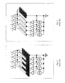
- FIG. 9 shows an example of the state-of-art wiring configuration of a bus system and power supply wires in a memory chip, e.g., a DRAM.
- FIG. 10 shows an example of a relatively simple embodiment where a latch-like structure, comprised of I 2 and I 3 , is added on the far-end side/receiving side of the bus system.
- FIG. 11 shows an example of a bus-wiring configuration which can lessen or remove the requirement that the near-end driver be stronger than the far-end latch-like structure.
- FIG. 12 shows an example of a bus-wiring configuration where the near-end and far-end of the bus line can be connected to a designated power supply wire when the bus line is not transferring data signal.
- FIG. 13 shows an example of a bus-wiring configuration where the near-end and far-end of the bus line can be connected to a designated power supply wire when the bus line is not transferring data signal.
- FIG. 14 shows an example of the state-of-art bus system circuit schematic for a memory chip.
- FIG. 15 shows an example of a bus system circuit schematic in a memory chip with the proposed modifications for power improvement.
- FIG. 16 illustrates an example of simple bus system architecture for a memory chip with the proposed improvements, when the bus system comprises of two buses.
- Various modifications and embodiments are possible as well, as described below and as would be readily apparent to one of ordinary skill in the art in view of the teachings of this application.
- the voltage drop/voltage glitch on power supply wires as well as the cross-talk effects between neighboring wires can be reduced by utilizing non-active signal wires.
- the non-active signal wires can be turned into power supply wires carrying a return current. That is, the extra wires carry the return current, and therefore improve the signal integrity (AC effect).
- the extra wires reduce the overall supply resistance to “far-located” circuits (DC effect). As shown in FIGS. 3 and 4 , the transient current/return current flows through the supply wires.
- non-active signal wires can act as additional supply power wires
- the transient current/return current that would have flowed through only the supply wires would also flow through not only the original supply wires but also the non-active wires.
- These non-active signal wires can be temporarily turned on during signal transmission period to temporarily act as virtual, additional power supply wires.
- these non-active signal wires can act as additional, virtual supply wires, the transient current/return current can have additional current paths that are connected in parallel. This can effectively reduce the total resistance and inductance, which the power supply wires will experience. If the effective, total resistance and inductance for the power supply wires can be reduced, the voltage drop/voltage glitch on the power supply wires can be reduced as well. Further, these non-active signal wires that can be temporarily turned on so as to act as additional power supply wires may be used with two-sided power connections in order to produce a shielding effect for the critical wires. This shielding effect can be further explained or defined by, for example, the following two effects:
- Electrostatic shielding effect Placing a 3rd wire (non-active signal wire) connected to one of supply potentials (VSS or VDD) between two wires (aggressor and victim) may reduce the effective capacitance from the aggressor-wire to the victim-wire. This method may work effectively if a shielding wire is low-resistance itself and has a low-resistive connection to GND or VDD.
- the shielding wire may bounce the following aggressor-wire, and a portion of those bounced can reach the victim-wire via an associated parasitic capacitance. Accordingly, connecting a 3rd wire to a shielding wire to supply a rail on both ends may reduce the effective shield resistance by half and therefore can improve the shielding effect.
- Electromagnetic shielding effect Two wires running in parallel over a long distance could be considered as one-turn windings of an air-core transformer.
- the direction of the magnetic field in the shielding loop would be opposite to that of the primary (aggressor) field, and in an ideal case, the two may compensate each other.
- Such transformer with one shorted winding can have close to zero efficiency—that is, there would exist very little coupling from aggressor to victim. Accordingly, this method can work effectively when the shielding trace/wire is connected on both ends. This means that the connections on those both ends would each provide a current loop.
- FIG. 8A An exemplary chip schematic implementing the above idea is shown in FIG. 8A .
- FIGS. 8B and 8C represent different connections that result in the circuit shown in FIG. 8A depending on whether the input signal to the circuit shown in FIG. 8A is at a logical 1/high state or a logical 0/low state.
- FIG. 8C shows an example of the electrical connection that would result when the input signal to the circuit shown in FIG. 8A is at a logical 1/high state.
- a signal of logic 1/high state is input to node IN.
- two transistors N-FETs N 1 and N 2 will be conducting, and resistance of signal wire R_signal will be connected in parallel to ground wiring resistance R_VSS.
- FIG. 8B shows an example of the electrical connection that would result when the input signal to the circuit shown in FIG. 8A is at a logical 0/low state.
- a signal of logic 0/low state is input to node IN.
- two transistors P-FETs P 1 and P 2 will be conducting, and thus resistance of signal wire R_signal will be connected in parallel with resistance of supply wire R_VDD through the two transistors, P-FETs P 1 and P 2 .
- the near-end inverter have a greater strength than the far-end latch circuit because if it is configured otherwise, the latch circuit on the far-end could keep the opposite logic states from the near-end inverter, which could result in a huge cross-current flow between the near-end inverter and the far-end latch circuit.
- FIG. 8A Although with one single circuit as shown in FIG. 8A may not be able to reduce the resistance and inductance of the power supply wires significant, the reduction may be substantial when a large number of wiring configurations employ the above circuit architecture, which is shown, for example, in FIG. 8A . In fact, many ICs nowadays have more than 50 wiring configurations, and in such environment, the cumulative effect of the above circuit architecture may be significant.
- a single memory array can receive around 50 unidirectional semi-static signals. If the trace width and the length for each signal are 0.25 um and 2000 um, respectively, the resistance of a single line/wiring is around 300 Ohm. If 50 ⁇ of these wirings are configured so as to be virtually connected in parallel, the resistance on these wirings can be reduced to be as small as 6 Ohm (300/50).
- FIG. 9 shows an example of the state-of-art wiring configuration of a bus system and power supply wires in a memory chip, e.g., a DRAM.
- the far-end signal is connected to gates of P-FET and N-FET of the inverter. No DC current is possible, and thus there can be no reduced resistance for the supply wires.
- a physical channel is provided to transfer from one circuit to another 100 signals therebetween, and the physical channel has a given length and is limited to 210 um-width. It is further assumed to deliver to remote circuit 30 mA of power supply current with allowed density of 1 mA per 1 um trace width.
- FIG. 10 shows an example of a relatively simple embodiment where a latch-like structure, comprised of I 2 and I 3 , is added on the far-end side/receiving side.
- the near-end driver is stronger than the far-end latch-like circuit, comprised of I 2 and I 3 , in order to guarantee proper switching of the signals. If the near-end driver is not stronger than the far-end latch inverter, there is a risk of the opposite logic states being stored and outputted due to the improper switching of the signals.
- the above problem can be lessened or completely removed. This can be achieved by reducing the risk of storing and outputting the erroneous, opposite logic states, which can occur due to improper signal switching when the near-end driver is not strong enough compared to the far-end latch-like circuit.
- FIG. 11 shows an example of a bus-wiring configuration which can lessen or remove the requirement that the near-end driver be stronger than the far-end latch-like structure.
- This can be achieved by adding an output enable signal, oe, to the output circuit so as to control the outputting of output signals config_out, as shown in FIG. 11 .
- This output enable signal oe is controlled by signal transf_en.
- Output enable signal oe is connected to the latch-like circuit, comprised of I 2 and I 3 , on the far-end side/receiving side. Then, output signal config_out can be outputted only when output enable signal oe is active. In other times, output signal config_out cannot be outputted.
- control signal transf_en corresponding to output enable signal oe, can be used to control the turn-on and turn-off states of the latch-like circuit on the far-end side, instead of just controlling the output signals.
- the near-end driver and the far-end latch-like circuit will not transfer signals when control signal transf_en is not active. Instead, when control signal transf_en is not active, the transferred signal values will have been stored in the latch-like structure on the far end, preventing storing erroneous signal values due to improper switching of the signals.
- control signal transf_en which corresponds to output enable signal oe, can be set at a logical 1/high state during bit update configurations so as to allow outputting of output signals config_out. At other times, control signal transf_en can be set at a logical 0/low state so as prevent the erroneous outputting of output signals config_out.
- the circuit can control the timing of storing and outputting the output signals so that such timing corresponds to the timings of signal transmission periods. Consequently, the risk of outputting the wrong signals, e.g., signals of opposite logic states that have been erroneously stored due to the improper switching of the signals when the near-end driver is not strong enough compared to the far-end latch, can be reduced.
- bus wirings can be configured so as to ensure a good connection to both supply wires VDD and VSS even when the all the bus wires carry a signal of logic 0 or a signal of logic 1. Exemplary implementations of such embodiments are shown in FIGS. 12 and 13 .
- bus wirings are configured so as to ensure a good connection to both supply wires VDD and VSS even when the all the bus wires carry a signal of logic 0 or a signal of logic 1, as shown, for example, in FIGS. 12 and 13 , the above problem can be mitigated or removed completely.
- connection of the wires can be configured such that the near-end and the far-end of a bus line is connected to a designated power supply wire when the bus line is not transferring data signal and supposed to be operating as an additional power supply wire.
- control signal transf_en when control signal transf_en is not active, the near-end and the far-end of a bus line is connected to supply wire via a pair of low resistive P-FETS P 1 and P 2 or via a pair of low resistive N-FETS N 1 and N 2 .
- control signal transf_en when control signal transf_en is not active, the near-end and the far-end of a bus line is connected to supply wire via a pair of low resistive P-FETS P 1 and P 2 or via a pair of low resistive N-FETS N 1 and N 2 .
- multiple non-active bus lines when multiple non-active bus lines are turned on to be used as additional power supply wires, they can each connect to their designated power supply wires, either VDD or VSS, so as to ensure that the power improvement is equally distributed between the two power supply wires, or in any other proportions as desired.
- the number of bus wires configured to connect to either supply wires via P-FETs or N-FETs can be set 50/50.
- the number of bus wires configured to connect to either supply wires via P-FETs or N-FETs can be set in accordance with the desired proportion.
- this embodiment can also reduce or remove the risk of storing and outputting the erroneous signals due to improper signal switching, which may occur when the near-end driver is not strong enough compared to the far-end latch, as the embodiment shown, for example, in FIG. 11 .
- the near-end driver when control signal transf_en is active, the near-end driver will be transferring signal values to the latch-like structure on the far end.
- control signal transf_en when control signal transf_en is not active, the transferred values will have been stored in the latch-like structure of I 3 and I 4 , and the further signal transferring becomes not possible because the bus wire associated with the non-active transf_en and oe will have been connected to one of the power supply wires via transistors. Therefore, the risk of storing and outputting the erroneous signals due to improper signal switching can be reduced or removed.
- FIG. 14 shows an example of the state-of-art bus system circuit schematic for a memory chip.
- Inverters I 1 , I 2 , I 5 and I 6 belong to high-data rate bus, which are represented as hf_signal ⁇ 0> and hf_signal ⁇ 1>.
- Inverters I 3 , I 4 , I 7 and I 8 belong to low data rate, which can be static, bus, which are represented as lf_signal ⁇ 0> and lf_signal ⁇ 1>. All the power supply is delivered through the path between VDD and GND, which is the same and only path for the return current as well.
- FIG. 15 shows an example of a bus system circuit schematic in a memory chip with the proposed modifications for power improvement.
- This configuration is similar to the embodiment shown in FIG. 11 in which output enable signal oe is connected to the latch-like structure so as to lessen or completely remove the requirement that the near-end driver be stronger than the far-end latch-like structure.
- the low data rate bus which can be static signals represented by lf_signal ⁇ 0> and lf_signal ⁇ 1>, are driven from the both sides, and these lines can provide additional connections to power supply wires. For example, lf_signal ⁇ 0> is connected in parallel to GND wire whereas lf_signal ⁇ 1> is connected in parallel to VDD wire.
- the placing of static signals in between the data transferring wires can also provide shielding effects for the neighboring data transferring wires, which can reduce the parasitic, magnetic and electrical coupling effects between the sensitive data transferring wires.
- FIG. 16 illustrates an example of simplified bus system architecture for a memory chip with the proposed improvements, when the bus system comprises of two buses.
- the proposed improvements can be achieved by utilizing the wires that belong to a non-active bus, a bus that is carrying low data rate or static signals, as extra power wires to reduce the effective resistance of the power wires, and also as extra shielding wires for shielding other wires that belong to another active bus, as well as extra current-path wires for providing current-paths for the return currents.
- the proposed improvements can also be realized by adding switches to power supplies in order to shorten the wires that belong to a non-active bus, or by changing the control of existing bidirectional bus drivers so that the non-active bus has both ends driven by the same signal at a logical 0 or 1.
- the proposed improvements can be implemented on the IC level or on the PCB level.
- the proposed improvements can be modified so as to displace all the power supply wires with the signal wires so that all the power deliveries are done via the signal wires.
Landscapes
- Engineering & Computer Science (AREA)
- Physics & Mathematics (AREA)
- Mathematical Physics (AREA)
- Computer Hardware Design (AREA)
- Computing Systems (AREA)
- General Engineering & Computer Science (AREA)
- Power Engineering (AREA)
- Microelectronics & Electronic Packaging (AREA)
- Semiconductor Integrated Circuits (AREA)
Abstract
Description
2) Electromagnetic shielding effect: Two wires running in parallel over a long distance could be considered as one-turn windings of an air-core transformer. If current is changed in a primary (aggressor) winding, there will be a corresponding current change in a secondary (victim) winding because of magnetic couplings between the two. For example, in case of a single-layer implementation, current return loop of an aggressor often has a big overlap with current return loop of a victim. Then, an inductive coupling between the two becomes strong enough to be visible. Meanwhile, adding a shielding wire, which is grounded on both ends, is equivalent to adding another of the above described air-core transformer—that is, one more single turn but shorted winding. In this case, any current change in the aggressor loop would create a (variable) magnetic field which would cause a current change in the shielding loop. The direction of the magnetic field in the shielding loop would be opposite to that of the primary (aggressor) field, and in an ideal case, the two may compensate each other. Such transformer with one shorted winding can have close to zero efficiency—that is, there would exist very little coupling from aggressor to victim. Accordingly, this method can work effectively when the shielding trace/wire is connected on both ends. This means that the connections on those both ends would each provide a current loop.
Claims (13)
Priority Applications (1)
| Application Number | Priority Date | Filing Date | Title |
|---|---|---|---|
| US14/274,307 US9508407B2 (en) | 2011-12-15 | 2014-05-09 | Wiring configuration of a bus system and power wires in a memory chip |
Applications Claiming Priority (2)
| Application Number | Priority Date | Filing Date | Title |
|---|---|---|---|
| US13/327,057 US8724360B2 (en) | 2011-12-15 | 2011-12-15 | Wiring configuration of a bus system and power wires in a memory chip |
| US14/274,307 US9508407B2 (en) | 2011-12-15 | 2014-05-09 | Wiring configuration of a bus system and power wires in a memory chip |
Related Parent Applications (1)
| Application Number | Title | Priority Date | Filing Date |
|---|---|---|---|
| US13/327,057 Continuation US8724360B2 (en) | 2011-12-15 | 2011-12-15 | Wiring configuration of a bus system and power wires in a memory chip |
Publications (2)
| Publication Number | Publication Date |
|---|---|
| US20140247681A1 US20140247681A1 (en) | 2014-09-04 |
| US9508407B2 true US9508407B2 (en) | 2016-11-29 |
Family
ID=48609972
Family Applications (2)
| Application Number | Title | Priority Date | Filing Date |
|---|---|---|---|
| US13/327,057 Active 2032-07-11 US8724360B2 (en) | 2011-12-15 | 2011-12-15 | Wiring configuration of a bus system and power wires in a memory chip |
| US14/274,307 Active 2031-12-24 US9508407B2 (en) | 2011-12-15 | 2014-05-09 | Wiring configuration of a bus system and power wires in a memory chip |
Family Applications Before (1)
| Application Number | Title | Priority Date | Filing Date |
|---|---|---|---|
| US13/327,057 Active 2032-07-11 US8724360B2 (en) | 2011-12-15 | 2011-12-15 | Wiring configuration of a bus system and power wires in a memory chip |
Country Status (1)
| Country | Link |
|---|---|
| US (2) | US8724360B2 (en) |
Cited By (1)
| Publication number | Priority date | Publication date | Assignee | Title |
|---|---|---|---|---|
| US10585817B2 (en) | 2018-05-29 | 2020-03-10 | Seagate Technology Llc | Method of signal integrity and power integrity analysis for address bus |
Families Citing this family (1)
| Publication number | Priority date | Publication date | Assignee | Title |
|---|---|---|---|---|
| US8724360B2 (en) * | 2011-12-15 | 2014-05-13 | Micron Technology, Inc. | Wiring configuration of a bus system and power wires in a memory chip |
Citations (10)
| Publication number | Priority date | Publication date | Assignee | Title |
|---|---|---|---|---|
| US5063304A (en) | 1990-04-27 | 1991-11-05 | Texas Instruments Incorporated | Integrated circuit with improved on-chip power supply control |
| US5500820A (en) * | 1992-09-30 | 1996-03-19 | Nec Corporation | Semiconductor memory device |
| US6724594B2 (en) | 2000-12-20 | 2004-04-20 | National Semiconductor Corporation | Over voltage protection test multiplexer and methods of operating the same |
| US6970369B2 (en) * | 2001-09-06 | 2005-11-29 | Elpida Memory, Inc. | Memory device |
| US7076757B2 (en) * | 2003-02-27 | 2006-07-11 | Nec Electronics Corporation | Semiconductor integrated device and apparatus for designing the same |
| US7102912B2 (en) | 2004-03-04 | 2006-09-05 | Infineon Technologies, Ag | Integrated semiconductor memory device and method for operating an integrated semiconductor memory device |
| US7315951B2 (en) * | 2003-10-27 | 2008-01-01 | Nortel Networks Corporation | High speed non-volatile electronic memory configuration |
| US7525856B2 (en) | 2007-04-04 | 2009-04-28 | Atmel Corporation | Apparatus and method to manage external voltage for semiconductor memory testing with serial interface |
| US7868656B2 (en) | 2005-09-26 | 2011-01-11 | Sgi International, Inc. | Hot plug control apparatus and method |
| US8724360B2 (en) * | 2011-12-15 | 2014-05-13 | Micron Technology, Inc. | Wiring configuration of a bus system and power wires in a memory chip |
-
2011
- 2011-12-15 US US13/327,057 patent/US8724360B2/en active Active
-
2014
- 2014-05-09 US US14/274,307 patent/US9508407B2/en active Active
Patent Citations (11)
| Publication number | Priority date | Publication date | Assignee | Title |
|---|---|---|---|---|
| US5063304A (en) | 1990-04-27 | 1991-11-05 | Texas Instruments Incorporated | Integrated circuit with improved on-chip power supply control |
| US5063304B1 (en) | 1990-04-27 | 1993-02-23 | Iyengar Narasimhan | |
| US5500820A (en) * | 1992-09-30 | 1996-03-19 | Nec Corporation | Semiconductor memory device |
| US6724594B2 (en) | 2000-12-20 | 2004-04-20 | National Semiconductor Corporation | Over voltage protection test multiplexer and methods of operating the same |
| US6970369B2 (en) * | 2001-09-06 | 2005-11-29 | Elpida Memory, Inc. | Memory device |
| US7076757B2 (en) * | 2003-02-27 | 2006-07-11 | Nec Electronics Corporation | Semiconductor integrated device and apparatus for designing the same |
| US7315951B2 (en) * | 2003-10-27 | 2008-01-01 | Nortel Networks Corporation | High speed non-volatile electronic memory configuration |
| US7102912B2 (en) | 2004-03-04 | 2006-09-05 | Infineon Technologies, Ag | Integrated semiconductor memory device and method for operating an integrated semiconductor memory device |
| US7868656B2 (en) | 2005-09-26 | 2011-01-11 | Sgi International, Inc. | Hot plug control apparatus and method |
| US7525856B2 (en) | 2007-04-04 | 2009-04-28 | Atmel Corporation | Apparatus and method to manage external voltage for semiconductor memory testing with serial interface |
| US8724360B2 (en) * | 2011-12-15 | 2014-05-13 | Micron Technology, Inc. | Wiring configuration of a bus system and power wires in a memory chip |
Non-Patent Citations (1)
| Title |
|---|
| Kuzmenka et al., U.S. Office Action mailed Sep. 12, 2013, directed to U.S. Appl. No. 13/327,057; 10 pages. |
Cited By (1)
| Publication number | Priority date | Publication date | Assignee | Title |
|---|---|---|---|---|
| US10585817B2 (en) | 2018-05-29 | 2020-03-10 | Seagate Technology Llc | Method of signal integrity and power integrity analysis for address bus |
Also Published As
| Publication number | Publication date |
|---|---|
| US8724360B2 (en) | 2014-05-13 |
| US20130155752A1 (en) | 2013-06-20 |
| US20140247681A1 (en) | 2014-09-04 |
Similar Documents
| Publication | Publication Date | Title |
|---|---|---|
| US6438014B2 (en) | High speed access compatible memory module | |
| US6411539B2 (en) | Memory system | |
| US6700823B1 (en) | Programmable common mode termination for input/output circuits | |
| US6674648B2 (en) | Termination cards and systems therefore | |
| JP2013534100A (en) | Balanced on-die termination | |
| US6771515B2 (en) | Systems having modules with on die terminations | |
| US20200321038A1 (en) | Driver circuit equipped with power gating circuit | |
| CN110970063A (en) | Apparatus and method for internal voltage generating circuit | |
| US9508407B2 (en) | Wiring configuration of a bus system and power wires in a memory chip | |
| CN101102641A (en) | Printed circuit board | |
| US10932358B2 (en) | Semiconductor devices and methods for enhancing signal integrity of an interface provided by a semiconductor device | |
| US6674649B2 (en) | Systems having modules sharing on module terminations | |
| US6724082B2 (en) | Systems having modules with selectable on die terminations | |
| US6711027B2 (en) | Modules having paths of different impedances | |
| US6208195B1 (en) | Fast transmission gate switch | |
| CN113380832A (en) | Output buffer circuit with metal option | |
| US6812869B1 (en) | Noise reduction techniques for programmable input/output circuits | |
| US6918078B2 (en) | Systems with modules sharing terminations | |
| US6717823B2 (en) | Systems having modules with buffer chips | |
| US10580499B2 (en) | Read only memory | |
| US5877930A (en) | Input and output noise reduction circuit | |
| US20040174807A1 (en) | Method for co-layout of different buses in an electric board | |
| US6631083B2 (en) | Systems with modules and clocking therefore | |
| US11783886B2 (en) | Semiconductor device capable of switching operation voltage | |
| US10637471B1 (en) | Termination circuit and semiconductor apparatus including the termination circuit |
Legal Events
| Date | Code | Title | Description |
|---|---|---|---|
| FEPP | Fee payment procedure |
Free format text: PAYOR NUMBER ASSIGNED (ORIGINAL EVENT CODE: ASPN); ENTITY STATUS OF PATENT OWNER: LARGE ENTITY |
|
| AS | Assignment |
Owner name: U.S. BANK NATIONAL ASSOCIATION, AS COLLATERAL AGENT, CALIFORNIA Free format text: SECURITY INTEREST;ASSIGNOR:MICRON TECHNOLOGY, INC.;REEL/FRAME:038669/0001 Effective date: 20160426 Owner name: U.S. BANK NATIONAL ASSOCIATION, AS COLLATERAL AGEN Free format text: SECURITY INTEREST;ASSIGNOR:MICRON TECHNOLOGY, INC.;REEL/FRAME:038669/0001 Effective date: 20160426 |
|
| AS | Assignment |
Owner name: MORGAN STANLEY SENIOR FUNDING, INC., AS COLLATERAL AGENT, MARYLAND Free format text: PATENT SECURITY AGREEMENT;ASSIGNOR:MICRON TECHNOLOGY, INC.;REEL/FRAME:038954/0001 Effective date: 20160426 Owner name: MORGAN STANLEY SENIOR FUNDING, INC., AS COLLATERAL Free format text: PATENT SECURITY AGREEMENT;ASSIGNOR:MICRON TECHNOLOGY, INC.;REEL/FRAME:038954/0001 Effective date: 20160426 |
|
| STCF | Information on status: patent grant |
Free format text: PATENTED CASE |
|
| AS | Assignment |
Owner name: U.S. BANK NATIONAL ASSOCIATION, AS COLLATERAL AGENT, CALIFORNIA Free format text: CORRECTIVE ASSIGNMENT TO CORRECT THE REPLACE ERRONEOUSLY FILED PATENT #7358718 WITH THE CORRECT PATENT #7358178 PREVIOUSLY RECORDED ON REEL 038669 FRAME 0001. ASSIGNOR(S) HEREBY CONFIRMS THE SECURITY INTEREST;ASSIGNOR:MICRON TECHNOLOGY, INC.;REEL/FRAME:043079/0001 Effective date: 20160426 Owner name: U.S. BANK NATIONAL ASSOCIATION, AS COLLATERAL AGEN Free format text: CORRECTIVE ASSIGNMENT TO CORRECT THE REPLACE ERRONEOUSLY FILED PATENT #7358718 WITH THE CORRECT PATENT #7358178 PREVIOUSLY RECORDED ON REEL 038669 FRAME 0001. ASSIGNOR(S) HEREBY CONFIRMS THE SECURITY INTEREST;ASSIGNOR:MICRON TECHNOLOGY, INC.;REEL/FRAME:043079/0001 Effective date: 20160426 |
|
| AS | Assignment |
Owner name: JPMORGAN CHASE BANK, N.A., AS COLLATERAL AGENT, ILLINOIS Free format text: SECURITY INTEREST;ASSIGNORS:MICRON TECHNOLOGY, INC.;MICRON SEMICONDUCTOR PRODUCTS, INC.;REEL/FRAME:047540/0001 Effective date: 20180703 Owner name: JPMORGAN CHASE BANK, N.A., AS COLLATERAL AGENT, IL Free format text: SECURITY INTEREST;ASSIGNORS:MICRON TECHNOLOGY, INC.;MICRON SEMICONDUCTOR PRODUCTS, INC.;REEL/FRAME:047540/0001 Effective date: 20180703 |
|
| AS | Assignment |
Owner name: MICRON TECHNOLOGY, INC., IDAHO Free format text: RELEASE BY SECURED PARTY;ASSIGNOR:U.S. BANK NATIONAL ASSOCIATION, AS COLLATERAL AGENT;REEL/FRAME:047243/0001 Effective date: 20180629 |
|
| AS | Assignment |
Owner name: MICRON TECHNOLOGY, INC., IDAHO Free format text: RELEASE BY SECURED PARTY;ASSIGNOR:MORGAN STANLEY SENIOR FUNDING, INC., AS COLLATERAL AGENT;REEL/FRAME:050937/0001 Effective date: 20190731 |
|
| AS | Assignment |
Owner name: MICRON SEMICONDUCTOR PRODUCTS, INC., IDAHO Free format text: RELEASE BY SECURED PARTY;ASSIGNOR:JPMORGAN CHASE BANK, N.A., AS COLLATERAL AGENT;REEL/FRAME:051028/0001 Effective date: 20190731 Owner name: MICRON TECHNOLOGY, INC., IDAHO Free format text: RELEASE BY SECURED PARTY;ASSIGNOR:JPMORGAN CHASE BANK, N.A., AS COLLATERAL AGENT;REEL/FRAME:051028/0001 Effective date: 20190731 |
|
| MAFP | Maintenance fee payment |
Free format text: PAYMENT OF MAINTENANCE FEE, 4TH YEAR, LARGE ENTITY (ORIGINAL EVENT CODE: M1551); ENTITY STATUS OF PATENT OWNER: LARGE ENTITY Year of fee payment: 4 |
|
| MAFP | Maintenance fee payment |
Free format text: PAYMENT OF MAINTENANCE FEE, 8TH YEAR, LARGE ENTITY (ORIGINAL EVENT CODE: M1552); ENTITY STATUS OF PATENT OWNER: LARGE ENTITY Year of fee payment: 8 |