US9507089B2 - Method of manufacturing a photonic integrated circuit optically coupled to a laser of III-V material - Google Patents
Method of manufacturing a photonic integrated circuit optically coupled to a laser of III-V material Download PDFInfo
- Publication number
- US9507089B2 US9507089B2 US14/804,629 US201514804629A US9507089B2 US 9507089 B2 US9507089 B2 US 9507089B2 US 201514804629 A US201514804629 A US 201514804629A US 9507089 B2 US9507089 B2 US 9507089B2
- Authority
- US
- United States
- Prior art keywords
- layer
- silicon
- iii
- trenches
- silicon layer
- Prior art date
- Legal status (The legal status is an assumption and is not a legal conclusion. Google has not performed a legal analysis and makes no representation as to the accuracy of the status listed.)
- Active
Links
Images


Classifications
-
- G—PHYSICS
- G02—OPTICS
- G02B—OPTICAL ELEMENTS, SYSTEMS OR APPARATUS
- G02B6/00—Light guides; Structural details of arrangements comprising light guides and other optical elements, e.g. couplings
- G02B6/10—Light guides; Structural details of arrangements comprising light guides and other optical elements, e.g. couplings of the optical waveguide type
- G02B6/12—Light guides; Structural details of arrangements comprising light guides and other optical elements, e.g. couplings of the optical waveguide type of the integrated circuit kind
- G02B6/13—Integrated optical circuits characterised by the manufacturing method
- G02B6/136—Integrated optical circuits characterised by the manufacturing method by etching
-
- G—PHYSICS
- G02—OPTICS
- G02B—OPTICAL ELEMENTS, SYSTEMS OR APPARATUS
- G02B6/00—Light guides; Structural details of arrangements comprising light guides and other optical elements, e.g. couplings
- G02B6/10—Light guides; Structural details of arrangements comprising light guides and other optical elements, e.g. couplings of the optical waveguide type
- G02B6/12—Light guides; Structural details of arrangements comprising light guides and other optical elements, e.g. couplings of the optical waveguide type of the integrated circuit kind
- G02B6/12004—Combinations of two or more optical elements
-
- G—PHYSICS
- G02—OPTICS
- G02B—OPTICAL ELEMENTS, SYSTEMS OR APPARATUS
- G02B6/00—Light guides; Structural details of arrangements comprising light guides and other optical elements, e.g. couplings
- G02B6/10—Light guides; Structural details of arrangements comprising light guides and other optical elements, e.g. couplings of the optical waveguide type
- G02B6/12—Light guides; Structural details of arrangements comprising light guides and other optical elements, e.g. couplings of the optical waveguide type of the integrated circuit kind
- G02B6/13—Integrated optical circuits characterised by the manufacturing method
- G02B6/132—Integrated optical circuits characterised by the manufacturing method by deposition of thin films
-
- G—PHYSICS
- G02—OPTICS
- G02B—OPTICAL ELEMENTS, SYSTEMS OR APPARATUS
- G02B6/00—Light guides; Structural details of arrangements comprising light guides and other optical elements, e.g. couplings
- G02B6/24—Coupling light guides
- G02B6/42—Coupling light guides with opto-electronic elements
- G02B6/4201—Packages, e.g. shape, construction, internal or external details
- G02B6/4256—Details of housings
- G02B6/4257—Details of housings having a supporting carrier or a mounting substrate or a mounting plate
-
- H—ELECTRICITY
- H01—ELECTRIC ELEMENTS
- H01S—DEVICES USING THE PROCESS OF LIGHT AMPLIFICATION BY STIMULATED EMISSION OF RADIATION [LASER] TO AMPLIFY OR GENERATE LIGHT; DEVICES USING STIMULATED EMISSION OF ELECTROMAGNETIC RADIATION IN WAVE RANGES OTHER THAN OPTICAL
- H01S5/00—Semiconductor lasers
- H01S5/02—Structural details or components not essential to laser action
- H01S5/0206—Substrates, e.g. growth, shape, material, removal or bonding
- H01S5/021—Silicon based substrates
-
- H—ELECTRICITY
- H01—ELECTRIC ELEMENTS
- H01S—DEVICES USING THE PROCESS OF LIGHT AMPLIFICATION BY STIMULATED EMISSION OF RADIATION [LASER] TO AMPLIFY OR GENERATE LIGHT; DEVICES USING STIMULATED EMISSION OF ELECTROMAGNETIC RADIATION IN WAVE RANGES OTHER THAN OPTICAL
- H01S5/00—Semiconductor lasers
- H01S5/02—Structural details or components not essential to laser action
- H01S5/022—Mountings; Housings
- H01S5/023—Mount members, e.g. sub-mount members
- H01S5/02325—Mechanically integrated components on mount members or optical micro-benches
-
- H—ELECTRICITY
- H01—ELECTRIC ELEMENTS
- H01S—DEVICES USING THE PROCESS OF LIGHT AMPLIFICATION BY STIMULATED EMISSION OF RADIATION [LASER] TO AMPLIFY OR GENERATE LIGHT; DEVICES USING STIMULATED EMISSION OF ELECTROMAGNETIC RADIATION IN WAVE RANGES OTHER THAN OPTICAL
- H01S5/00—Semiconductor lasers
- H01S5/02—Structural details or components not essential to laser action
- H01S5/026—Monolithically integrated components, e.g. waveguides, monitoring photo-detectors, drivers
-
- H—ELECTRICITY
- H01—ELECTRIC ELEMENTS
- H01S—DEVICES USING THE PROCESS OF LIGHT AMPLIFICATION BY STIMULATED EMISSION OF RADIATION [LASER] TO AMPLIFY OR GENERATE LIGHT; DEVICES USING STIMULATED EMISSION OF ELECTROMAGNETIC RADIATION IN WAVE RANGES OTHER THAN OPTICAL
- H01S5/00—Semiconductor lasers
- H01S5/30—Structure or shape of the active region; Materials used for the active region
- H01S5/34—Structure or shape of the active region; Materials used for the active region comprising quantum well or superlattice structures, e.g. single quantum well [SQW] lasers, multiple quantum well [MQW] lasers or graded index separate confinement heterostructure [GRINSCH] lasers
- H01S5/343—Structure or shape of the active region; Materials used for the active region comprising quantum well or superlattice structures, e.g. single quantum well [SQW] lasers, multiple quantum well [MQW] lasers or graded index separate confinement heterostructure [GRINSCH] lasers in AIIIBV compounds, e.g. AlGaAs-laser, InP-based laser
-
- G—PHYSICS
- G02—OPTICS
- G02B—OPTICAL ELEMENTS, SYSTEMS OR APPARATUS
- G02B6/00—Light guides; Structural details of arrangements comprising light guides and other optical elements, e.g. couplings
- G02B6/10—Light guides; Structural details of arrangements comprising light guides and other optical elements, e.g. couplings of the optical waveguide type
- G02B6/12—Light guides; Structural details of arrangements comprising light guides and other optical elements, e.g. couplings of the optical waveguide type of the integrated circuit kind
- G02B2006/12083—Constructional arrangements
- G02B2006/121—Channel; buried or the like
-
- G—PHYSICS
- G02—OPTICS
- G02B—OPTICAL ELEMENTS, SYSTEMS OR APPARATUS
- G02B6/00—Light guides; Structural details of arrangements comprising light guides and other optical elements, e.g. couplings
- G02B6/10—Light guides; Structural details of arrangements comprising light guides and other optical elements, e.g. couplings of the optical waveguide type
- G02B6/12—Light guides; Structural details of arrangements comprising light guides and other optical elements, e.g. couplings of the optical waveguide type of the integrated circuit kind
- G02B2006/12083—Constructional arrangements
- G02B2006/12121—Laser
-
- H—ELECTRICITY
- H01—ELECTRIC ELEMENTS
- H01S—DEVICES USING THE PROCESS OF LIGHT AMPLIFICATION BY STIMULATED EMISSION OF RADIATION [LASER] TO AMPLIFY OR GENERATE LIGHT; DEVICES USING STIMULATED EMISSION OF ELECTROMAGNETIC RADIATION IN WAVE RANGES OTHER THAN OPTICAL
- H01S5/00—Semiconductor lasers
- H01S5/005—Optical components external to the laser cavity, specially adapted therefor, e.g. for homogenisation or merging of the beams or for manipulating laser pulses, e.g. pulse shaping
- H01S5/0085—Optical components external to the laser cavity, specially adapted therefor, e.g. for homogenisation or merging of the beams or for manipulating laser pulses, e.g. pulse shaping for modulating the output, i.e. the laser beam is modulated outside the laser cavity
Definitions
- the present disclosure relates to a method of manufacturing an integrated circuit comprising photonic components on silicon and a laser made of III-V material, with one of the photonic components being a waveguide optically coupled to the laser.
- Passive or active photonic components such as waveguides, coupling structures, modulators, photodetectors, for example, may be formed in a semiconductor layer, such as silicon, and may be associated to form a photonic integrated circuit.
- a semiconductor layer such as silicon
- an interconnection structure encapsulated in an insulating region is arranged on a surface of the silicon layer.
- the interconnection structure comprises a plurality of metallization levels connected together and to the photonic components by electrically-conductive vias.
- a known advantageous photonic component is a laser comprising an amplifying medium made of a composite III-V semiconductor material optically coupled to a waveguide of a photonic integrated circuit.
- a wafer of III-V materials comprising the laser elements may be placed on the silicon layer having the photonic components formed therein.
- An interconnection structure is arranged on a front surface of a silicon layer, and a layer of III-V materials is arranged on a rear surface side of the silicon layer.
- a method of forming the above assembly and a photonic integrated circuit associated with a III-V laser is provided.
- an embodiment provides a method of manufacturing an integrated circuit comprising photonic components on the silicon layer and a laser made of a III-V group material.
- the method may comprise the successive steps of a) providing the silicon layer having a front surface and a rear surface, with the rear surface being laid on a first insulating layer that is laid on a support; b) etching from the front surface to form first trenches through the silicon layer, stopping on the first insulating layer, and covering the walls and the bottom of the first trenches with a silicon nitride layer; c) etching from the front surface to form second trenches through a portion of a thickness of the silicon layer, the second trenches being formed at a location of at least some of the photonic components; d) filling the first and second silicon oxide trenches and planarizing the same to the front surface; e) removing the support and the first insulating layer, stopping on the rear surface and on the nitride layer; and f) bonding, on the rear surface
- the method may comprise, between steps d) and e), the successive steps of g) covering the front surface with a second insulating layer; h) above a first trench, etching third trenches through the second insulating layer and the silicon oxide, stopping on the nitride layer, and filling the third trenches with a first metal to form first conductive vias; and i) forming, on the front surface, an interconnection structure comprising a metallization level in contact with the first conductive vias.
- the method may further comprise, after step f), the successive steps of j) covering the interconnection structure and the laser with an insulating region having a planar exposed surface; and k) etching, opposite the rear side of the first vias, fourth trenches through the insulating region, stopping on the nitride layer, etching exposed portions of the nitride layer, and filling the fourth trenches with a second metal to form second conductive vias.
- the method may comprise, at step h), a step of etching fifth trenches through the second insulating layer all the way to contacting regions of the photonic components of the integrated circuit, and a step of filling the fifth trenches with the first metal to form third conductive vias.
- the material of the first insulating layer may be silicon oxide.
- the method may further comprise, at step f), depositing a silicon oxide layer on the rear surface prior to the bonding of the III-V wafer.
- the III-V heterostructure may successively comprise, from the rear surface, a layer of doped III-V materials of a first conductivity type, a stack of III-V materials capable of forming quantum wells, and a layer of a doped III-V material of the second conductivity type.
- the III-V plate may be bonded by molecular bonding at step f).
- a thickness of the silicon nitride layer may be in the range from 10 to 100 nm.
- a photonic integrated circuit comprises an interconnection structure arranged on a front surface of a silicon layer, and a laser comprising III-V composite materials on a rear surface of the silicon layer.
- photonic components including at least one waveguide may be optically coupled with the laser.
- Each photonic component may be delimited by first trenches extending from the front surface all the way to the rear surface.
- Each first trench may be coated with a silicon nitride layer and may be filled with silicon oxide.
- At least some of the components comprising second trenches may be filled with silicon oxide extending from the front surface across a portion of a thickness of the silicon layer.
- the photonic integrated circuit may further comprise at least one first via extending from a metallization level of the interconnection structure to the bottom of the first trench.
- the circuit may further comprise at least one second via extending from the exposed surface of an insulating layer encapsulating the laser to at least one of the first vias.
- FIGS. 1 to 10 are simplified cross-sectional views illustrating successive steps of an embodiment of a method of manufacturing a photonic integrated circuit associated with a III-V laser.
- FIGS. 1 to 10 are simplified cross-sectional views illustrating successive steps of an embodiment of a method of manufacturing a photonic integrated circuit comprising photonic components formed in a semiconductor layer, such as silicon, and a III-V laser optically coupled to a waveguide in the photonic integrated circuit.
- deep trenches 1 have been etched in an SOI-type (Silicon On Insulator) silicon layer 3 having a rear surface F 1 on an insulating layer 5 .
- the insulating layer 5 may be, for example, a silicon oxide layer, designated by the acronym BOX (Buried OXide).
- BOX Buried OXide
- the front surface F 2 of the silicon layer 3 may be coated with one or more protection layers, such as a silicon oxide layer 9 , for example.
- the silicon oxide layer 9 may be coated with a silicon nitride layer 11 .
- the etching of trenches 1 is performed from the front surface F 2 of the silicon layer 3 all the way to the rear surface F 1 of the silicon layer 3 .
- a silicon nitride layer 13 is deposited on the exposed surface of the structure so that the walls and the bottom of the deep trenches 1 are coated. Deep trenches 1 delimit portions of the silicon layer 3 where integrated photonic components will be formed.
- trenches may be much wider than the others. Some of the wider trenches are intended, as will be discussed below, to receive interconnection vias.
- a single wider trench 1 ′ is shown in the figures.
- the support 7 is a silicon wafer.
- the thickness of the silicon layer 3 is, for example, in the range of 200 nm to 1 ⁇ m and may be equal to 300 nm.
- the thickness of the insulating layer 5 is, for example, in the range of 500 nm to 2.5 ⁇ m and may be equal to 700 nm.
- the thickness of the nitride layer 13 is, for example, in the range of 10 to 100 nm and may be equal to 30 nm.
- FIG. 2 shows the structure after etching partial trenches 15 in the silicon layer 3 .
- the partial trenches 15 are etched from the front surface F 2 of the silicon layer 3 across only a portion of a thickness of this layer.
- a depth of the the partial trenches 15 is typically approximately half the thickness of the silicon layer 3 .
- Forming of the partial trenches 15 is followed by the deposition and the planarizing of silicon oxide 17 so as to fill the trenches 1 , 1 ′ and 15 .
- the silicon oxide 17 is deposited by chemical vapor deposition, for example.
- Waveguides 19 and 21 , a coupler 23 , and a modulator 25 are separated by the deep trenches 1 have been shown as an example.
- Each of these photonic components is conventionally defined in the silicon layer by the shape, position, and dimensions of partial trenches 15 filled with silicon oxide 17 .
- FIG. 3 shows the structure after a planarization that stops on the front surface F 2 of the silicon layer 3 .
- This step may be carried out by chemical mechanical polishing, for example.
- Steps of implanting doping species may be carried out to form one or more of N- or P-type doped regions in the silicon layer 3 to form doped regions of the integrated photonic modulator 25 .
- Contacting regions 27 are then formed for contacting these doped regions.
- FIG. 4 shows the structure after deposition of an insulating layer 29 on the front surface F 2 , such as a silicon oxide layer, for example, followed by etching trenches 31 and 33 from the upper surface of the insulating layer 29 .
- the trenches 31 extend through the insulating layer 29 all the way to the contacting regions 27 .
- the trenches 33 formed adjacent or opposite the trench 1 ′, extend through the insulating layer 29 and through the silicon oxide 17 so as to fill the trench 1 ′ all the way to the nitride layer 13 while coating the bottom of the trench 1 ′.
- the insulating layer 5 i.e., BOX
- FIG. 5 shows the structure after filling the trenches 31 and 33 with a metal to form conductive vias which will also be designated with the same references 31 and 33 .
- the metal of the respective vias 31 and 33 may be tungsten.
- the interconnection structure comprises metallization levels 39 separated by insulating regions generally designated with reference numeral 35 , and associated by vias 41 .
- the front side of each of the vias 31 and 33 is in contact with portions of at least some of the metallization levels 39 so that some of the photonic components are connected via the interconnection structure.
- Metallization levels 39 and vias 41 may be made of copper.
- the insulating regions 35 may comprise stacks of silicon oxide and silicon nitride layers, for example. The thickness of the assembly of the insulating regions 35 is in the range of 2 ⁇ m to 5 ⁇ m and may be equal to approximately 3 ⁇ m, for example.
- a portion 43 of one of these levels may be formed opposite the coupler 23 .
- the metal layer portion 43 forms a mirror to reflect light originating from the coupler 23 .
- a handle 37 is then fastened by molecular bonding, for example, to the upper surface of the insulating regions 35 of the interconnection structure.
- the handle may be a silicon wafer, for example.
- FIG. 6 shows the structure of FIG. 5 after flipping and removal of the support 7 and the insulating layer 5 .
- the insulating layer 5 is removed from the rear surface F 1 of the silicon layer 3 and on the nitride layer 13 .
- the removal of the silicon oxide forming the insulating layer 5 may not be exactly stopped on the silicon oxide 17 filling the trenches 1 and 1 ′. If not exactly stopped, this would cause the structure to have a non-planar upper surface (i.e., on the rear surface F 1 of the silicon layer 3 in FIG. 6 ).
- the rear surface F 1 of the silicon layer 3 is then coated with a thin silicon oxide layer 45 having a thickness, for example, in the range of 10 to 300 nm and may be equal to 100 nm. Since the presence of the silicon nitride layer 13 results in the rear surface F 1 being planar, the upper surface of the thin silicon oxide layer is also planar.
- the thin silicon oxide layer 45 is coated with an amorphous silicon layer 47 which is also coated with a thin silicon oxide layer 49 having an upper surface that is also planar.
- the thickness of the amorphous silicon layer 47 is, for example, in the range from 200 nm to 300 nm and may be equal to approximately 200 nm.
- FIG. 7 shows the structure onto which, on the, side of the rear surface F 1 , a wafer or a chip comprising a heterostructure 51 of composite III-V semiconductor materials has been attached by molecular bonding.
- the heterostructure 51 comprises, from the side of the rear surface F 1 , a layer 53 comprising an N-type doped III-V group semiconductor material, a stack of layers 55 forming quantum wells, and a layer 57 of a P-type doped composite III-V group semiconductor material.
- the heterostructure is initially on a support such as an InP substrate separated from the layer 57 by an etch stop layer. The support and the etch stop layer may be removed by etching the molecular bonding of the wafer or the chip comprising the heterostructure 51 .
- the layer 53 may be a stack of InP and InGaAs layers.
- the thickness of the layer 53 may be approximately 200 nm, for example.
- the stack of layers 55 forming the quantum wells comprises InGaAsP layers.
- a thickness of the stack 55 may be on the order of 300 nm.
- the layer 57 is made of InP, for example.
- the thickness of the heterostructure 51 after removal of the support is, for example, in the range of 2 to 10 ⁇ m and may be equal to approximately 3 ⁇ m.
- the presence of the silicon nitride layer 13 allows for a structure having its upper surface coated with a thin silicon oxide having a planar upper surface to be obtained, as shown in FIG. 6 .
- the molecular bonding of the wafer 51 on this layer is particularly satisfactory.
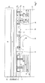
- FIG. 8 shows the structure after etching the wafer 51 and the layers 49 and 47 .
- a first etching is performed from the upper surface of the wafer 51 all the way to the thin layer 45 while leaving in place, preferably opposite the waveguide 19 , portions of the layers 47 and 49 .
- the layers 47 and 49 have a portion at least topped with portions of the layers 53 , 55 , and 57 of the wafer 51 .
- a second etching is performed to remove lateral portions of the remaining portions of the layers 55 and 57 .
- the remaining portions of the layers 53 , 55 , and 57 form the III-V amplifying medium 59 of a laser.
- the remaining portion of the layer 47 forms the coupler 61 , such as a waveguide, for example, that optically couples the amplifying medium 59 to the waveguide 19 formed in the silicon layer 3 .
- etch steps are followed by forming contacting regions 63 on the amplifying medium 59 . More particularly, the contacting regions 63 are formed at the level of the upper surfaces of the remaining portions of the layers 57 and 53 .
- An insulating region 65 is then deposited on the side of the rear surface F 1 over the entire structure.
- the insulating region 65 may extend from the thin silicon oxide layer 45 to a level higher than that of the upper surface of the amplifying medium 59 .
- the insulating region is, for example, a planarized silicon oxide layer.
- FIG. 9 shows the structure after etching of the trenches 67 and 69 .
- Each trench 67 extends from the upper surface of the insulating region 65 to a contacting region 63 .
- Each trench 69 is arranged opposite a via 33 and extends from the upper surface of the insulating region 65 to the silicon nitride layer 13 coating the bottom of the trench 1 ′.
- FIG. 10 shows the structure after etching the portion of the silicon nitride layer 13 arranged at the bottom of the trenches 69 to expose the metal of the vias 33 on the upper side thereof. This etch step is followed by the filling of the trenches 67 and 69 with a metal to form conductive vias which will also be designated with reference numerals 67 and 69 .
- the coupler 61 may be arranged on the side of the front surface F 2 of the silicon layer 3 .
- the deposition on the surface F 2 of a thin silicon oxide layer, of an amorphous silicon, and of another thin silicon oxide layer is then etched to form a coupler. It can thus be understood that the steps of the manufacturing method may be added or suppressed and that the order in which these steps are carried out may be modified.
- a resonant cavity optically coupled to the waveguide 19 and to amplifying medium 59 of the laser may be conventionally formed by those skilled in the art.
- the cavity may be farmed by etching Bragg networks at the level of the waveguide 19 or at the level of the coupler 61 .
- the insulating layer 5 (BOX) is made of a same material as that filling the deep trenches 1 and 1 ′ (e.g., silicon oxide), have been discussed. These advantages also remain when the materials of these regions are different and the removal of the material of the insulating layer 5 (BOX) is performed by etching, which is non-selective over the material filing the trenches 1 and 1 ′.
- the arrangement, the shape, and the number of vias 31 , 33 , 41 , 57 , and 69 , of metallization levels 39 , and of photonic components 19 , 21 , 23 , and 25 may be adapted by those skilled in the art.
- Other photonic components such as a photodetector may also be formed in the silicon layer 3 .
Landscapes
- Physics & Mathematics (AREA)
- General Physics & Mathematics (AREA)
- Optics & Photonics (AREA)
- Engineering & Computer Science (AREA)
- Microelectronics & Electronic Packaging (AREA)
- Condensed Matter Physics & Semiconductors (AREA)
- Electromagnetism (AREA)
- Semiconductor Lasers (AREA)
- Optical Integrated Circuits (AREA)
Abstract
Description
Claims (20)
Applications Claiming Priority (2)
| Application Number | Priority Date | Filing Date | Title |
|---|---|---|---|
| FR1457861 | 2014-08-18 | ||
| FR1457861A FR3024910A1 (en) | 2014-08-18 | 2014-08-18 | METHOD FOR MANUFACTURING A PHOTONIC INTEGRATED CIRCUIT OPTICALLY COUPLED TO A LASER IN A MATERIAN III-V |
Publications (2)
| Publication Number | Publication Date |
|---|---|
| US20160047986A1 US20160047986A1 (en) | 2016-02-18 |
| US9507089B2 true US9507089B2 (en) | 2016-11-29 |
Family
ID=52450258
Family Applications (1)
| Application Number | Title | Priority Date | Filing Date |
|---|---|---|---|
| US14/804,629 Active US9507089B2 (en) | 2014-08-18 | 2015-07-21 | Method of manufacturing a photonic integrated circuit optically coupled to a laser of III-V material |
Country Status (2)
| Country | Link |
|---|---|
| US (1) | US9507089B2 (en) |
| FR (1) | FR3024910A1 (en) |
Cited By (5)
| Publication number | Priority date | Publication date | Assignee | Title |
|---|---|---|---|---|
| US10340656B2 (en) | 2016-06-30 | 2019-07-02 | Commissariat A L'energie Atomique Et Aux Energies Alternatives | Semiconductor laser source |
| CN110574162A (en) * | 2019-08-02 | 2019-12-13 | 长江存储科技有限责任公司 | Three-dimensional memory device and method of making the same |
| US10877211B2 (en) * | 2013-06-24 | 2020-12-29 | Stmicroelectronics Sa | Methods of fabricating integrated circuit devices with components on both sides of a semiconductor layer |
| WO2025103077A1 (en) | 2023-11-16 | 2025-05-22 | 湖北九峰山实验室 | Integration method of modular silicon-based heterogeneous optoelectronic integration architecture |
| FR3158372A1 (en) | 2024-01-17 | 2025-07-18 | Scintil Photonics | Photonic device comprising a component layer arranged on a support substrate and method for preparing such a photonic device |
Families Citing this family (8)
| Publication number | Priority date | Publication date | Assignee | Title |
|---|---|---|---|---|
| FR3054926B1 (en) | 2016-08-08 | 2018-10-12 | Commissariat A L'energie Atomique Et Aux Energies Alternatives | METHOD FOR MANUFACTURING PROPAGATION LOSS MODULATOR AND PROPAGATION INDEX OF OPTICAL SIGNAL |
| FR3082354B1 (en) | 2018-06-08 | 2020-07-17 | Commissariat A L'energie Atomique Et Aux Energies Alternatives | PHOTONIC CHIP CROSSED BY A VIA |
| CN110692138B (en) * | 2019-08-02 | 2021-04-27 | 长江存储科技有限责任公司 | Three-dimensional memory device and method of making the same |
| CN112635489B (en) * | 2019-08-02 | 2024-09-06 | 长江存储科技有限责任公司 | Three-dimensional memory device and method for manufacturing the same |
| CN111180458B (en) * | 2020-01-02 | 2022-12-02 | 长江存储科技有限责任公司 | 3D memory device and method of manufacturing the same |
| CN111162046B (en) * | 2020-01-02 | 2023-01-13 | 长江存储科技有限责任公司 | Three-dimensional stacked structure and preparation method |
| US11487059B2 (en) * | 2021-02-19 | 2022-11-01 | Globalfoundries U.S. Inc. | Photonics integrated circuit with silicon nitride waveguide edge coupler |
| EP4664165A1 (en) * | 2024-06-11 | 2025-12-17 | Nokia Solutions and Networks Oy | Semiconductor device and semiconductor device fabrication method |
Citations (4)
| Publication number | Priority date | Publication date | Assignee | Title |
|---|---|---|---|---|
| US20030036123A1 (en) | 1997-09-18 | 2003-02-20 | Genentech, Inc. | Secreted and transmembrane polypeptides and nucleic acids encoding the same |
| US20100142580A1 (en) | 2006-12-05 | 2010-06-10 | Commissariat A L'energie Atomique | Laser device with coupled laser source and waveguide |
| US20130082294A1 (en) | 2011-09-30 | 2013-04-04 | Kabushiki Kaisha Toshiba | Semiconductor light-emitting device and manufacturing method of the same |
| US20140044391A1 (en) | 2012-08-09 | 2014-02-13 | Kabushiki Kaisha Toshiba | Optical interconnection device and method of manufacturing the same |
Family Cites Families (1)
| Publication number | Priority date | Publication date | Assignee | Title |
|---|---|---|---|---|
| US20030036213A1 (en) * | 2001-08-16 | 2003-02-20 | Motorola, Inc. | Optical switch with multiplexed data and control signals separated by group velocity dispersion |
-
2014
- 2014-08-18 FR FR1457861A patent/FR3024910A1/en not_active Withdrawn
-
2015
- 2015-07-21 US US14/804,629 patent/US9507089B2/en active Active
Patent Citations (4)
| Publication number | Priority date | Publication date | Assignee | Title |
|---|---|---|---|---|
| US20030036123A1 (en) | 1997-09-18 | 2003-02-20 | Genentech, Inc. | Secreted and transmembrane polypeptides and nucleic acids encoding the same |
| US20100142580A1 (en) | 2006-12-05 | 2010-06-10 | Commissariat A L'energie Atomique | Laser device with coupled laser source and waveguide |
| US20130082294A1 (en) | 2011-09-30 | 2013-04-04 | Kabushiki Kaisha Toshiba | Semiconductor light-emitting device and manufacturing method of the same |
| US20140044391A1 (en) | 2012-08-09 | 2014-02-13 | Kabushiki Kaisha Toshiba | Optical interconnection device and method of manufacturing the same |
Cited By (11)
| Publication number | Priority date | Publication date | Assignee | Title |
|---|---|---|---|---|
| US10877211B2 (en) * | 2013-06-24 | 2020-12-29 | Stmicroelectronics Sa | Methods of fabricating integrated circuit devices with components on both sides of a semiconductor layer |
| US10340656B2 (en) | 2016-06-30 | 2019-07-02 | Commissariat A L'energie Atomique Et Aux Energies Alternatives | Semiconductor laser source |
| CN110574162A (en) * | 2019-08-02 | 2019-12-13 | 长江存储科技有限责任公司 | Three-dimensional memory device and method of making the same |
| CN110574162B (en) * | 2019-08-02 | 2021-02-12 | 长江存储科技有限责任公司 | Three-dimensional memory device and method of manufacturing the same |
| US11094714B2 (en) | 2019-08-02 | 2021-08-17 | Yangtze Memory Technologies Co., Ltd. | Three-dimensional memory devices and fabricating methods thereof |
| TWI803732B (en) * | 2019-08-02 | 2023-06-01 | 大陸商長江存儲科技有限責任公司 | 3d memory device and method of fabricating the same |
| US12402309B2 (en) | 2019-08-02 | 2025-08-26 | Yangtze Memory Technologies Co., Ltd. | Three-dimensional memory devices and fabricating methods thereof |
| WO2025103077A1 (en) | 2023-11-16 | 2025-05-22 | 湖北九峰山实验室 | Integration method of modular silicon-based heterogeneous optoelectronic integration architecture |
| EP4645614A1 (en) | 2023-11-16 | 2025-11-05 | Hubei Jiufengshan Laboratory | Integration method of modular silicon-based heterogeneous optoelectronic integration architecture |
| FR3158372A1 (en) | 2024-01-17 | 2025-07-18 | Scintil Photonics | Photonic device comprising a component layer arranged on a support substrate and method for preparing such a photonic device |
| WO2025153192A1 (en) | 2024-01-17 | 2025-07-24 | Scintil Photonics | Photonic device comprising a layer of components arranged on a support substrate and method for preparing such a photonic device |
Also Published As
| Publication number | Publication date |
|---|---|
| US20160047986A1 (en) | 2016-02-18 |
| FR3024910A1 (en) | 2016-02-19 |
Similar Documents
| Publication | Publication Date | Title |
|---|---|---|
| US9507089B2 (en) | Method of manufacturing a photonic integrated circuit optically coupled to a laser of III-V material | |
| US10877211B2 (en) | Methods of fabricating integrated circuit devices with components on both sides of a semiconductor layer | |
| US9461441B2 (en) | Integrated hybrid laser source compatible with a silicon technology platform, and fabrication process | |
| US11784456B2 (en) | Method of manufacturing a III-V based optoelectronic device | |
| US11075498B2 (en) | Method of fabricating an optoelectronic component | |
| US20090294814A1 (en) | Three-Dimensional Integrated Circuits and Techniques for Fabrication Thereof | |
| JP2020519011A5 (en) | ||
| US20140264723A1 (en) | Devices including a diamond layer | |
| KR102007258B1 (en) | Method of fabricating optoelectronic substrate | |
| JP2019161229A (en) | Photonic device comprising laser optically connected to silicon waveguide and method for manufacturing such photonic device | |
| US10139563B2 (en) | Method for making photonic chip with multi-thickness electro-optic devices and related devices | |
| KR20160114516A (en) | Semiconductor device and manufacturing method thereof | |
| CN111373541B (en) | Methods for transferring light emitting structures | |
| US20210384700A1 (en) | Method for Processing a Laser Device | |
| WO2018065776A1 (en) | Frontend integration of electronics and photonics | |
| US20180026111A1 (en) | Low-resistive, cmos-compatible, au-free ohmic contact to n-inp | |
| CN112713214B (en) | Method for fabricating photonic chips by transferring wafers to receiving substrates | |
| US12360311B2 (en) | Process for fabricating a photonics-on-silicon optoelectronic system comprising an optical device coupled to an integrated photonic circuit | |
| JP6676795B2 (en) | Optoelectronic device and method | |
| CN117420635A (en) | Optical device and method of manufacturing the same | |
| JPWO2019026943A1 (en) | Optical semiconductor device manufacturing method and optical semiconductor device | |
| US12147105B2 (en) | Waveguide of an SOI structure | |
| US20250309609A1 (en) | Semiconductor optical device and method of manufacturing semiconductor optical device | |
| CN117995780A (en) | Semiconductor device and method for manufacturing the same |
Legal Events
| Date | Code | Title | Description |
|---|---|---|---|
| AS | Assignment |
Owner name: STMICROELECTRONICS (CROLLES 2) SAS, FRANCE Free format text: ASSIGNMENT OF ASSIGNORS INTEREST;ASSIGNOR:CREMER, SEBASTIEN;REEL/FRAME:036180/0694 Effective date: 20150407 Owner name: STMICROELECTRONICS SA, FRANCE Free format text: ASSIGNMENT OF ASSIGNORS INTEREST;ASSIGNOR:CHANTRE, ALAIN;REEL/FRAME:036180/0671 Effective date: 20150407 |
|
| STCF | Information on status: patent grant |
Free format text: PATENTED CASE |
|
| MAFP | Maintenance fee payment |
Free format text: PAYMENT OF MAINTENANCE FEE, 4TH YEAR, LARGE ENTITY (ORIGINAL EVENT CODE: M1551); ENTITY STATUS OF PATENT OWNER: LARGE ENTITY Year of fee payment: 4 |
|
| AS | Assignment |
Owner name: STMICROELECTRONICS INTERNATIONAL N.V., SWITZERLAND Free format text: ASSIGNMENT OF ASSIGNORS INTEREST;ASSIGNOR:STMICROELECTRONICS SA;REEL/FRAME:063277/0222 Effective date: 20230123 Owner name: STMICROELECTRONICS INTERNATIONAL N.V., SWITZERLAND Free format text: ASSIGNMENT OF ASSIGNORS INTEREST;ASSIGNOR:STMICROELECTRONICS (CROLLES 2) SAS;REEL/FRAME:063276/0569 Effective date: 20230119 |
|
| MAFP | Maintenance fee payment |
Free format text: PAYMENT OF MAINTENANCE FEE, 8TH YEAR, LARGE ENTITY (ORIGINAL EVENT CODE: M1552); ENTITY STATUS OF PATENT OWNER: LARGE ENTITY Year of fee payment: 8 |