US9507076B2 - Backlight unit and liquid crystal display device including the same - Google Patents
Backlight unit and liquid crystal display device including the same Download PDFInfo
- Publication number
- US9507076B2 US9507076B2 US13/461,435 US201213461435A US9507076B2 US 9507076 B2 US9507076 B2 US 9507076B2 US 201213461435 A US201213461435 A US 201213461435A US 9507076 B2 US9507076 B2 US 9507076B2
- Authority
- US
- United States
- Prior art keywords
- light sources
- blocks
- reflective
- guide plate
- reflective patterns
- Prior art date
- Legal status (The legal status is an assumption and is not a legal conclusion. Google has not performed a legal analysis and makes no representation as to the accuracy of the status listed.)
- Active, expires
Links
Images


Classifications
-
- G—PHYSICS
- G02—OPTICS
- G02F—OPTICAL DEVICES OR ARRANGEMENTS FOR THE CONTROL OF LIGHT BY MODIFICATION OF THE OPTICAL PROPERTIES OF THE MEDIA OF THE ELEMENTS INVOLVED THEREIN; NON-LINEAR OPTICS; FREQUENCY-CHANGING OF LIGHT; OPTICAL LOGIC ELEMENTS; OPTICAL ANALOGUE/DIGITAL CONVERTERS
- G02F1/00—Devices or arrangements for the control of the intensity, colour, phase, polarisation or direction of light arriving from an independent light source, e.g. switching, gating or modulating; Non-linear optics
- G02F1/01—Devices or arrangements for the control of the intensity, colour, phase, polarisation or direction of light arriving from an independent light source, e.g. switching, gating or modulating; Non-linear optics for the control of the intensity, phase, polarisation or colour
- G02F1/13—Devices or arrangements for the control of the intensity, colour, phase, polarisation or direction of light arriving from an independent light source, e.g. switching, gating or modulating; Non-linear optics for the control of the intensity, phase, polarisation or colour based on liquid crystals, e.g. single liquid crystal display cells
- G02F1/133—Constructional arrangements; Operation of liquid crystal cells; Circuit arrangements
- G02F1/1333—Constructional arrangements; Manufacturing methods
- G02F1/1335—Structural association of cells with optical devices, e.g. polarisers or reflectors
-
- G—PHYSICS
- G02—OPTICS
- G02B—OPTICAL ELEMENTS, SYSTEMS OR APPARATUS
- G02B6/00—Light guides; Structural details of arrangements comprising light guides and other optical elements, e.g. couplings
- G02B6/0001—Light guides; Structural details of arrangements comprising light guides and other optical elements, e.g. couplings specially adapted for lighting devices or systems
- G02B6/0011—Light guides; Structural details of arrangements comprising light guides and other optical elements, e.g. couplings specially adapted for lighting devices or systems the light guides being planar or of plate-like form
- G02B6/0033—Means for improving the coupling-out of light from the light guide
- G02B6/0058—Means for improving the coupling-out of light from the light guide varying in density, size, shape or depth along the light guide
-
- G—PHYSICS
- G02—OPTICS
- G02B—OPTICAL ELEMENTS, SYSTEMS OR APPARATUS
- G02B6/00—Light guides; Structural details of arrangements comprising light guides and other optical elements, e.g. couplings
- G02B6/0001—Light guides; Structural details of arrangements comprising light guides and other optical elements, e.g. couplings specially adapted for lighting devices or systems
- G02B6/0011—Light guides; Structural details of arrangements comprising light guides and other optical elements, e.g. couplings specially adapted for lighting devices or systems the light guides being planar or of plate-like form
- G02B6/0013—Means for improving the coupling-in of light from the light source into the light guide
- G02B6/0023—Means for improving the coupling-in of light from the light source into the light guide provided by one optical element, or plurality thereof, placed between the light guide and the light source, or around the light source
- G02B6/003—Lens or lenticular sheet or layer
-
- G—PHYSICS
- G02—OPTICS
- G02B—OPTICAL ELEMENTS, SYSTEMS OR APPARATUS
- G02B6/00—Light guides; Structural details of arrangements comprising light guides and other optical elements, e.g. couplings
- G02B6/0001—Light guides; Structural details of arrangements comprising light guides and other optical elements, e.g. couplings specially adapted for lighting devices or systems
- G02B6/0011—Light guides; Structural details of arrangements comprising light guides and other optical elements, e.g. couplings specially adapted for lighting devices or systems the light guides being planar or of plate-like form
- G02B6/0033—Means for improving the coupling-out of light from the light guide
- G02B6/0035—Means for improving the coupling-out of light from the light guide provided on the surface of the light guide or in the bulk of it
- G02B6/0036—2-D arrangement of prisms, protrusions, indentations or roughened surfaces
-
- G—PHYSICS
- G02—OPTICS
- G02B—OPTICAL ELEMENTS, SYSTEMS OR APPARATUS
- G02B6/00—Light guides; Structural details of arrangements comprising light guides and other optical elements, e.g. couplings
- G02B6/0001—Light guides; Structural details of arrangements comprising light guides and other optical elements, e.g. couplings specially adapted for lighting devices or systems
- G02B6/0011—Light guides; Structural details of arrangements comprising light guides and other optical elements, e.g. couplings specially adapted for lighting devices or systems the light guides being planar or of plate-like form
- G02B6/0033—Means for improving the coupling-out of light from the light guide
- G02B6/0035—Means for improving the coupling-out of light from the light guide provided on the surface of the light guide or in the bulk of it
- G02B6/004—Scattering dots or dot-like elements, e.g. microbeads, scattering particles, nanoparticles
- G02B6/0043—Scattering dots or dot-like elements, e.g. microbeads, scattering particles, nanoparticles provided on the surface of the light guide
-
- G—PHYSICS
- G02—OPTICS
- G02B—OPTICAL ELEMENTS, SYSTEMS OR APPARATUS
- G02B6/00—Light guides; Structural details of arrangements comprising light guides and other optical elements, e.g. couplings
- G02B6/0001—Light guides; Structural details of arrangements comprising light guides and other optical elements, e.g. couplings specially adapted for lighting devices or systems
- G02B6/0011—Light guides; Structural details of arrangements comprising light guides and other optical elements, e.g. couplings specially adapted for lighting devices or systems the light guides being planar or of plate-like form
- G02B6/0033—Means for improving the coupling-out of light from the light guide
- G02B6/005—Means for improving the coupling-out of light from the light guide provided by one optical element, or plurality thereof, placed on the light output side of the light guide
- G02B6/0055—Reflecting element, sheet or layer
-
- G—PHYSICS
- G02—OPTICS
- G02B—OPTICAL ELEMENTS, SYSTEMS OR APPARATUS
- G02B6/00—Light guides; Structural details of arrangements comprising light guides and other optical elements, e.g. couplings
- G02B6/0001—Light guides; Structural details of arrangements comprising light guides and other optical elements, e.g. couplings specially adapted for lighting devices or systems
- G02B6/0011—Light guides; Structural details of arrangements comprising light guides and other optical elements, e.g. couplings specially adapted for lighting devices or systems the light guides being planar or of plate-like form
- G02B6/0066—Light guides; Structural details of arrangements comprising light guides and other optical elements, e.g. couplings specially adapted for lighting devices or systems the light guides being planar or of plate-like form characterised by the light source being coupled to the light guide
- G02B6/0068—Arrangements of plural sources, e.g. multi-colour light sources
-
- G—PHYSICS
- G02—OPTICS
- G02B—OPTICAL ELEMENTS, SYSTEMS OR APPARATUS
- G02B6/00—Light guides; Structural details of arrangements comprising light guides and other optical elements, e.g. couplings
- G02B6/0001—Light guides; Structural details of arrangements comprising light guides and other optical elements, e.g. couplings specially adapted for lighting devices or systems
- G02B6/0011—Light guides; Structural details of arrangements comprising light guides and other optical elements, e.g. couplings specially adapted for lighting devices or systems the light guides being planar or of plate-like form
- G02B6/0075—Arrangements of multiple light guides
- G02B6/0078—Side-by-side arrangements, e.g. for large area displays
Definitions
- the present invention relates to a backlight unit and a liquid crystal display (LCD) device and more particularly to an edge type backlight unit being capable of performing a local dimming driving and scan driving and an LCD device including the same.
- LCD liquid crystal display
- LCD devices which are widely used for TV, monitors, TV, and so on because of their high contrast ratio and other characteristics that are suitable to display moving images, display images using an optical anisotropy and polarization properties of liquid crystal molecules.
- the LCD device includes a liquid crystal panel.
- the liquid crystal panel includes a first substrate where a gate line, a data line, a thin film transistor and a pixel electrode are formed, a second substrate where a color filter layer and a common electrode are formed, and a liquid crystal layer which includes the liquid crystal molecules interposed therebetween.
- the alignment direction of the liquid crystal molecules is changed by an electric field in the liquid crystal panel such that light transmissivity is also controlled.
- the liquid crystal panel does not include a light source therein, an additional light source is required.
- a backlight unit including a light source is disposed under the liquid crystal panel to provide light onto the liquid crystal panel.
- the LCD device can display images using the light from the backlight unit.
- a fluorescent lamp such as a cold cathode fluorescent lamp (CCFL) and an external electrode fluorescent lamp (EEFL) has been widely used as the light source of the backlight unit.
- CCFL cold cathode fluorescent lamp
- EEFL external electrode fluorescent lamp
- LED light emitting diode
- the backlight unit is classified into an edge light type and a direct type depending on a position of the light source.
- the direct type backlight unit the light source is positioned throughout directly under the liquid crystal panel such that the light from the light source is directly provided to the liquid crystal panel.
- a light guide plate is disposed under the liquid crystal panel, and the light source is positioned at a side of the light guide plate. The light from the light source in the edge type backlight unit is refracted by the light guide plate to proceed to the liquid crystal panel.
- the direct type backlight unit In the direct type backlight unit, a local dimming where different voltages can be applied to each LED such that each LED emits light having a difference in brightness, or a scan driving where different voltages can be applied to each LED string, can be performed. However, more LEDs are required and thus power consumption is increased for the direct type backlight unit than the edge type backlight unit.
- the edge type backlight unit has advantages in a production process, weight, a thin profile and power consumption.
- the edge type backlight unit has limitations in a scan driving and a local dimming driving in comparison with the direct type backlight unit.
- an LCD device having a backlight unit that can provide advantages in weight, a thin profile, power consumption, image quality, etc. is desired.
- the present invention is directed to a backlight unit and an LCD device including the backlight unit that substantially obviate one or more of the problems due to limitations and disadvantages of the related art.
- An object of the present invention is to provide an edge type backlight unit capable of performing local dimming driving and scan driving.
- Another object of the present invention is to provide an LCD device including the backlight unit and having advantages in weight, power consumption, image quality, and so on.
- a backlight unit includes a light guide plate including a body, a light path changing pattern having a lens shape on a top surface of the body and a plurality of reflective patterns on a bottom surface of the body; and a light source facing at least one side surface of the body, wherein a plurality of dot blocks are defined in columns and rows on the bottom surface of the body, and the reflective patterns are formed at a part of the plurality of dot blocks.
- a liquid crystal display device in another aspect, includes a liquid crystal panel; and a backlight unit providing a light to the liquid crystal panel, the backlight unit including: a light guide plate including a body, a light path changing pattern having a lens shape on a top surface of the body and a plurality of reflective patterns on a bottom surface of the body; and a light source facing at least one side surface of the body, wherein a plurality of dot blocks are defined in columns and rows on the bottom surface of the body, and the reflective patterns are formed a part of the plurality of dot blocks.
- the present invention provides a backlight unit for a display device, comprising: a light source configured to generate light; and a light guide plate configured to distribute the light received from the light source, the light guide plate including: at least one body, each of the at least one body divided into a plurality of blocks, and a plurality of reflective patterns formed on a bottom surface of the body, wherein the plurality of reflective patterns are selectively provided at some of the plurality of blocks.
- the present invention provides a liquid crystal display device, comprising: a liquid crystal panel; and a backlight unit configured to provide light to the liquid crystal panel, the backlight unit including a light source configured to generate the light and a light guide plate configured to distribute the light received from the light source, the light guide plate including: at least one body, each of the at least one body divided into a plurality of blocks, and a plurality of reflective patterns formed on a bottom surface of the body, wherein the plurality of reflective patterns are selectively provided at some of the plurality of blocks.
- FIG. 1 is a schematic block diagram of a liquid crystal display device according to an embodiment of the present invention.
- FIG. 2 is a schematic cross-sectional view of an LCD device according to an embodiment of the present invention.
- FIG. 3 is a schematic perspective view of an LED assembly and a light guide plate for a backlight unit according to according to an embodiment of the present invention
- FIG. 4 is a schematic plane view of a rear side of an LED assembly and a light guide plate for a backlight unit according to an embodiment of the present invention
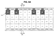
- FIGS. 5A and 5B are views illustrating an example of local dimming driving in a backlight unit according to an embodiment of the present invention
- FIGS. 6A and 6B are views illustrating an example of scan driving in a backlight unit according to an embodiment of the present invention.
- FIG. 7 is a schematic cross-sectional view of an LCD device according to an embodiment of the present invention.
- FIG. 8 is a schematic plane view of a rear side of an LED assembly and a light guide plate for a backlight unit according to an embodiment of the present invention.
- FIG. 1 is a schematic block diagram of a liquid crystal display device according to an embodiment of the present invention
- FIG. 2 is a schematic cross-sectional view of an LCD device according to an embodiment of the present invention.
- an LCD device 100 includes a liquid crystal panel 110 for displaying images, a backlight unit 120 for providing light to the liquid crystal panel 110 , a gate driver 164 for applying a gate signal to the gate lines 113 of the liquid crystal panel 110 , a data driver 166 for applying a data signal to the data lines 115 of the liquid crystal panel 110 , a timing controller 162 for receiving an image signal and a control signal from an outer circuit part and providing a gate control signal to the gate driver 164 and RGB data and a data control signal to the data driver 166 , and a backlight driver 168 for receiving a dimming signal or a scan signal from the timing controller 162 and controlling a power of the backlight unit 120 .
- the liquid crystal panel 110 is a main part for displaying images and includes a first substrate 112 , a second substrate 114 facing the first substrate 112 , and a liquid crystal layer provided between the first and second substrates 112 and 114 .
- the gate lines 113 and data lines 115 crossing each other are provided to define a plurality of pixel regions P, and a thin film transistor (TFT) Tr connected to the corresponding gate and data lines 113 and 115 is formed at each intersection of the gate line 113 and data line 115 .
- TFT thin film transistor
- a black matrix for shielding non-display elements such as the gate lines 113 , the data lines 115 and the TFTs Tr, and a color filter layer may be formed.
- the color filter layer can include red, green and blue color filter patterns and corresponds to the pixel regions P.
- the liquid crystal capacitor Clc includes a pixel electrode and a common electrode.
- the pixel electrode and the common electrode may be formed on the first substrate 112 such that a horizontal electric field is generated therebetween.
- the pixel electrode and the common electrode may be formed on the first and second substrates 112 and 114 , respectively, such that a vertical electric field is generated therebetween.
- first and second polarization plates 119 a and 119 b may be formed.
- the gate driver 164 and the data driver 166 respectively providing the gate signals and the data signals to the gate lines 113 and the data lines 115 are combined along at least one side of the liquid crystal panel 110 as a printed circuit board where a gate driving integrated circuit and a data driving circuit board can be installed.
- the timing controller 162 may be formed on the printed circuit board.
- various types of liquid display panels may be provided as the panel 110 .
- the timing controller 162 receives signals such as an image signal, a data enable (DE), a horizontal synchronization signal (HSY), a horizontal synchronization signal (VSY), a clock signal (CLK) and so on, and generates RGB data, the data control signal and the gate control signal.
- the timing controller 162 analyzes the data signal in each frame and generates a dimming signal for driving the LEDs in a dot block or a scan signal for driving the LEDs in a line block.
- the dimming signal or the scan signal is provided to the backlight driver 168 .
- the timing controller 162 analyzes the data signal and converts the data signal in the dot block or the line block to have a higher gray level and generates the dimming signal or the scan signal having a lower duty ratio.
- the backlight driver 168 receiving the dimming signal or the scan signal applies a current to the LEDs in the dot block or the line block such that the LEDs in the dot block or the line block provides light with a lower brightness to the liquid crystal panel 110 . Since the image in the dot block or the line block has the lower brightness, a contrast ratio can be improved.
- the brightness decrease in the dot block or the line block is performed by reducing the applied current, and the applied current decrease is performed by reducing the duty ratio.
- the duty ratio preferably means a ratio of a time of applying on-voltage to a time of applying off-voltage. As the duty ratio is reduced, the LCD device 100 can have a lower power consumption with a high contrast ratio.
- the timing controller 162 when the data signal having a high brightness is concentrated on the dot block or the line block, a contrast ratio can be improved by increasing a current applied to the LEDs. Namely, the timing controller 162 generates a dimming signal or a scan signal having a higher duty ratio and provides it to the backlight driver 168 . Although not shown, to generate the dimming signal or the scan signal, the timing controller 162 may further includes a histogram analyzer, a data converter and a duty ratio converter.
- the backlight unit 120 includes a light guide plate 123 under the liquid crystal panel 110 , a first LED assembly 128 as a first light source, a second LED assembly 129 as a second light source, a reflective sheet 125 under the light guide plate 123 , one or more diffusion sheets 124 between the light guide plate 123 and the liquid crystal panel 110 , and one or more optical sheets 121 between the diffusion sheet 124 and the liquid crystal panel 110 .
- the first LED assembly 128 includes first LEDs 128 a on a first printed circuit board (PCB) 128 b
- the second LED assembly 129 includes second LEDs 129 a on a second PCB 129 b.
- the first LED assembly 128 and the second LED assembly 129 are positioned at opposite sides of the light guide plate 123 .
- the first and second LED assemblies 128 and 129 are positioned horizontal sides of the light guide plate 123 .
- the first LEDs 128 a in the first LED assembly 128 are horizontally arranged
- the second LEDs 129 a in the first LED assembly 129 are horizontally arranged.
- the first and second LEDs 128 a and 129 a are arranged along a direction of the gate lines 113 . This may be called as a horizontal edge type backlight unit or a horizontal edge type LCD device.
- the light from the first and second LEDs 128 a and 129 a is refracted and reflected through the light guide plate 123 and provided onto the back of the liquid crystal panel 110 .
- Each of the first and second PCBs 128 b and 129 b may be a metal core PCB having a heat emitting property.
- a heat emitting plate may be formed such that heat from the LEDs 128 a and 129 a are emitted to the outer space.
- the reflective sheet 125 is disposed under the light guide plate 123 and reflects the light toward the liquid crystal panel 110 .
- the reflective sheet 125 extends to cover the entire bottom surface of the light guide plate 13 .
- the diffusion sheet 124 is disposed over the light guide plate 123 to improve brightness uniformity.
- the optical sheet 121 is disposed on the diffusion sheet 124 to diffuse or concentrate the light and provide it toward the liquid crystal panel 110 .
- the optical sheet 121 may include a diffusion sheet and at least one light concentration sheet.
- a gap having a predetermined size is provided between the top surface of the light guide plate 123 and a bottom surface of the diffusion sheet 124 . This gap is preferably an air gap.
- the liquid crystal panel 110 and the backlight unit 120 are combined using a main frame 130 , a top frame 140 and a bottom frame 150 .
- the main frame 130 surrounds edges of the liquid crystal panel 110 .
- the top frame 140 cover edges of the liquid crystal panel 110 and sides of the main frame 130 , so the top frame 140 can support and protect of the edges of the liquid crystal panel 110 and sides of the main frame 130 .
- the top frame 140 has an opening to expose a center area of the liquid crystal panel 110 .
- the bottom frame 50 includes a bottom surface covering a rear side of the backlight unit 120 and four side surfaces perpendicularly extending from the bottom surface.
- the first and second LED assemblies 128 and 129 are arranged at two opposite side surfaces of the bottom frame 150 .
- the main frame 130 is combined with the top frame 140 and the bottom frame 150 for modulation.
- the top frame 140 may be called as a top case, a top cover or a case top, and the main frame 130 may be called as a guide panel, a main support or a mold frame.
- the bottom frame 150 may be called as a bottom cover or a lower cover.
- the first and second LEDs 128 a and 129 a emit the light toward the light guide plate 123 , and the light is provided onto the liquid crystal panel 110 through the light guide plate 123 , the reflective sheet 125 , the diffusion sheet 124 and the optical sheet 121 .
- FIG. 3 is a schematic perspective view of an LED assembly and a light guide plate of a backlight unit of a display device according to according to an embodiment of the present invention
- FIG. 4 is a schematic plane view of a rear side of an LED assembly and a light guide plate of a backlight unit of a display device according to an embodiment of the present invention.
- the first and second LED assemblies 128 and 129 are arranged at opposite sides of the light guide plate 123 .
- the first and second LED assemblies 128 and 129 are arranged at two longer sides of the light guide plate 123 .
- this may be called as the horizontal edge type backlight unit.
- the first and second LED assemblies 128 and 129 are arranged at two horizontal sides. At each longer side of the light guide plate 123 , one or more LED assemblies may be disposed.
- the light path changing pattern 123 c is formed on a top surface of the body 123 a of the light guide plate 123 and entirely covers the top surface of the body 123 a .
- the light path changing pattern 123 c includes a plurality of lenses 123 c 1 protruding from the top surface of the body 123 a .
- the lenses 123 c 1 preferably have a semi-circle shape or a semi-ellipse shape and extend along the shorter side of the light guide plate 123 .
- the lenses 123 c 1 can be any element that has a lenticular shape on its top surface. In other words, the lenses 123 c 1 are arranged along the longer side of the light guide plate 123 where each lens extends along the shorter side of the light guide plate 12 .
- the lenses 123 c 1 have the semi-circle or semi-ellipse shape, the lenses 123 c 1 can be different shapes or configurations. That is, the light path changing pattern 123 c can in other pattern or shape.
- two lenses 123 c 1 correspond to one first LED 128 a .
- at least one LED 128 a corresponds to at least one lens 123 c 1 or each LED 128 a can correspond to multiple lenses 123 c 1 so that the light from one LED 128 can propagate through the multiple lenses 123 c 1 of the body 123 b .
- Other variations are possible.
- the light path changing pattern 123 c guides the light from the first and second LEDs 128 a and 129 a . Namely, a straight path of the light from the first and second LEDs 128 a and 129 a is secured due to the light path changing pattern 123 c . Accordingly, the light refracted and reflected in the light path changing pattern 123 c can travel through the light guide plate 123 in a helix shape.
- the reflective patterns 123 b are formed at the bottom surface of the body 123 a of the light guide plate 123 and partially or selectively cover the bottom surface of the body 123 a .
- the reflective patterns 123 b are alternately arranged in the columns and the rows as shown in FIG. 4 .
- the reflective patterns 123 b are formed at a part of the dot blocks A 1 - 1 to A 4 - 11 such that the bottom surface of the body 123 a with the reflective patterns 123 b has a check pattern shape.
- the reflective patterns 123 b are formed at the first, third, fifth . . . eleventh dot blocks A 1 - 1 , A 1 - 3 , A 1 - 5 and A 1 - 11 in the first row and at the second, fourth, sixth . . . tenth dot blocks A 2 - 2 , A 2 - 4 , A 2 - 6 . . . A 2 - 10 in the second row.
- the reflective patterns 123 b are formed at the first, third, fifth . . . eleventh dot blocks A 3 - 1 , A 3 - 3 , A 3 - 5 and A 3 - 11 in the third row and at the second, fourth, sixth . . . tenth dot blocks A 4 - 2 , A 4 - 4 , A 4 - 6 . . . A 4 - 10 in the fourth row.
- the reflective patterns 123 b are formed at odd-numbered dot blocks in odd-numbered rows and at even-numbered dot blocks in even-numbered rows.
- the reflective patterns 123 b may be formed at the even-numbered dot blocks in the odd-numbered rows and at the odd-numbered dot blocks in the even-numbered rows.
- the present invention is not limited thereto and can have a different number of dot blocks between two opposing LEDs of the backlight, where some of the dot blocks can selectively have the reflective patterns 123 b to provide an enhanced local dimming operation and an enhanced scanning operation.
- the dot blocks can selectively have the reflective patterns 123 b between two opposing LEDs of the backlight.
- the reflective patterns 123 b may be provided only in the first and fourth dot blocks.
- the second and fifth dot blocks may only have the reflective patterns 123 b .
- the third and sixth dot blocks may only have the reflective patterns.
- the set of such three columns of dot blocks is repeatedly and continuously provided between the sets of opposing LEDs 128 a and 129 a .
- all the reflective patterns 123 b of the light guide plate form multiple diagonal lines. This concept is equally applicable to other embodiments such as the embodiment of FIG. 7 .
- the reflective patterns 123 b 1 may be formed in the n/2 dot blocks while the other remaining dot blocks do not have the reflective patterns.
- the reflective patterns 123 b are formed in a checker pattern. Then, if the reflective pattern 123 b is disposed at one dot block, the reflective pattern 123 b is not disposed at adjacent four dot blocks with respect to that one dot block. Also, when the reflective pattern 123 b is not disposed at another one dot block, the reflective pattern 123 b is disposed at adjacent four dot blocks with respect to the another one dot block.
- one of the dot blocks A 1 - 1 to A 4 - 11 corresponds to one of the LEDs 128 a and 129 a .
- one of the dot blocks A 1 - 1 to A 4 - 11 may correspond to at least one of the LEDs 128 a and 129 a .
- Each reflective pattern 123 b has a smaller size than a corresponding one of the dot block A 1 - 1 to A 4 - 11 . Namely, a width M and a length L of the reflective pattern 123 b is smaller than those of each of the dot blocks A 1 - 1 to A 4 - 11 . Since the light is spread by the reflective patterns 123 b and the light path changing pattern 123 c , it is desirable for the reflective pattern 123 b to have a smaller size than each of the dot blocks A 1 - 1 to A 4 - 11 .
- FIG. 2 shows the reflective pattern 123 b concaving toward the body 123 a .
- the reflective pattern 123 b may be embossed or protruded from the body 123 b toward the reflective sheet 125 whereas
- FIG. 4 shows that each reflective pattern may be composed of a plurality of reflective dots 123 b 1 or dot like elements.
- Each reflective dot 123 b 1 in the reflective pattern 123 b may be a semi-circle shape, a semi-ellipse shape, a polygonal shape, a hologram pattern, or other shape.
- FIG. 4 shows that the reflective dots 123 b 1 are uniformly arranged.
- the reflective dots 123 b 1 having the same size may be more densely disposed as the reflective dots 123 b 1 are at a farther distance from the LEDs 128 a or 129 a .
- a density of the reflective dots 123 b 1 is proportional to its distance from the LEDs.
- the reflective dots 123 b 1 may be larger and have a smaller distance therebetween as the reflective dots 123 b 1 are at a farther distance from the LEDs 128 a or 129 a.
- the body 123 a of the light guide plate 123 may be formed of polymethylmethacrylate (PMMA) or polymethacrylstyrene as a mixture of PMMA and polystyrene.
- PMMA polymethylmethacrylate
- polymethacrylstyrene as a mixture of PMMA and polystyrene.
- the 1st to 11th dot blocks A 1 - 1 to A 1 - 11 in the first row are defined as a first line block B 1
- the 1st to 11th dot blocks A 2 - 1 to A 2 - 11 in the second row are defined as a second line block B 2
- the 1st to 11th dot blocks A 3 - 1 to A 3 - 11 in the third row are defined as a third line block B 3
- the 1st to 11th dot blocks A 4 - 1 to A 4 - 11 in the fourth row are defined as a fourth line block B 4 .
- the reflective patterns 123 b in the 2nd, 4th . . . 10th dot blocks A 2 - 2 , A 2 - 4 . . . A 2 - 10 respectively correspond to the 2nd, 4th . . .
- the reflective patterns 123 b in the 2nd, 4th . . . 10th dot blocks A 4 - 2 , A 4 - 4 . . . A 4 - 10 respectively correspond to the 2nd, 4th . . . 10th LEDs 129 a of the second LED assembly 129 .
- Brightness in the dot blocks A 1 - 1 to A 4 - 11 depends on the LEDs 128 a and 129 a and the reflective patterns 123 b .
- the light from the LEDs affect not only the dot blocks where the reflective patterns 123 b are formed, but also affect the dot blocks where the reflective patterns 123 b are not formed, in the same row and adjacent to the dot blocks.
- the light through not only the first and third dot blocks A 1 - 1 and A 1 - 3 but also through the second and fourth dot blocks A 1 - 2 and A 1 - 4 (which are adjacent to the first and third dot blocks A 1 - 1 and A 1 - 3 ) is provided as a strong plane light.
- the second dot blocks A 1 - 2 which is disposed between the first and third dot blocks A 1 - 1 and A 1 - 3 , is strongly affected by the first and third LEDs 1 and 3 and the reflective patterns 123 b in the first and third dot blocks A 1 - 1 and A 1 - 3 .
- a uniform light distribution through the light guide plate 123 can be provided.
- FIGS. 5A and 5B are views illustrating an example of local dimming driving in a backlight unit according to an embodiment of the present invention
- FIGS. 6A and 6B are views illustrating an example of scan driving in a backlight unit according to an embodiment of the present invention.
- the backlight unit driven in a local dimming or a scan driving is illustrated with references to FIGS. 5A, 5B, 6A and 6B with FIGS. 1-4 .
- FIGS. 5A and 5B An example of local dimming performed using the backlight unit of the present invention is explained with FIGS. 5A and 5B .
- the backlight driver 168 (of FIG. 1 ), which is controlled by the timing controller 162 of FIG. 1 applies a dimming signal having a first duty ratio to the 1st, 3rd, 7th and 9th LEDs 1 , 3 , 7 and 9 of the first LED assembly 128 , then the 1st, 3rd, 7th and 9th LEDs 1 , 3 , 7 and 9 of the first LED assembly 128 emit light toward the corresponding parts of the light guide plate 123 .
- the light is then refracted and reflected by the light path changing pattern 123 c and the reflective patterns 123 b such that the plane light is provided in the 1st, 3rd, 7th and 9th dot blocks A 1 - 1 , A 1 - 3 , A 1 - 7 and A 1 - 9 of the first row.
- the light in the 1st, 3rd, 7th and 9th dot blocks A 1 - 1 , A 1 - 3 , A 1 - 7 and A 1 - 9 of the first row has higher a brightness than other dot blocks. Accordingly, the contrast ratio is increased by using the local dimming method.
- the backlight driver 168 (of FIG. 1 ), which is controlled by the timing controller 162 of FIG. 1 applies a dimming signal having the first duty ratio to the 1st, 4th, 8th and 11th LEDs 1 , 4 , 8 and 11 of the first LED assembly 128
- the 1st, 4th, 8th and 11th LEDs 1 , 4 , 8 and 11 of the first LED assembly 128 emit the light toward the corresponding parts of the light guide plate 123 .
- the light in the 1st dot block A 1 - 1 and the 11th dot block A 1 - 11 of the first row and the 4th dot block A 2 - 4 and the 8th dot block A 2 - 8 of the second row has a higher brightness than other dot blocks. Accordingly, the contrast ratio is increased and the local dimming is performed by using the selectively positioned reflective patterns 123 b of the backlight unit of the present invention.
- FIGS. 6A and 6B An example of scan driving performed using the backlight unit of the present invention is explained with FIGS. 6A and 6B .
- the backlight driver 168 (of FIG. 1 ), which is controlled by the timing controller 162 of FIG. 1 applies a scan signal having a second duty ratio, which is larger than the first duty ratio, to the 1st, 3rd, 5th, 7th, 9th and 11th LEDs 1 , 3 , 5 , 7 , 9 and 11 of the first LED assembly 128 , then the 1st, 3rd, 5th, 7th, 9th and 11th LEDs 1 , 3 , 5 , 7 , 9 and 11 of the first LED assembly 128 emit light to the corresponding parts of the light guide plate 123 .
- the light is then refracted and reflected by the light path changing pattern 123 c and the reflective patterns 123 b such that the plane light is provided in the 1st, 3rd, 5th, 7th, 9th and 11th dot blocks A 1 - 1 , A 1 - 3 , A 1 - 5 , A 1 - 7 , A 1 - 9 and A 1 - 11 of the first row.
- the scan signal has the second duty ratio, which is larger than the first duty ratio applied to the LEDs in the local dimming
- the current applied to the 1st, 3rd, 5th, 7th, 9th and 11th LEDs 1 , 3 , 5 , 7 , 9 and 11 of the first LED assembly 128 is higher such that the light in the 1st, 3rd, 5th, 7th, 9th and 11th dot blocks A 1 - 1 , A 1 - 3 , A 1 - 5 , A 1 - 7 , A 1 - 9 and A 1 - 11 of the first row affects the 2nd, 4th, 6th, 8th and 10th dot blocks A 1 - 2 , A 1 - 4 , A 1 - 6 , A 1 - 8 and A- 10 in the first row.
- the plane light is provided through all dot blocks A 1 - 1 , A 1 - 2 . . . A 1 - 11 in the first line block B 1 .
- the gap between the light guide plate 123 and the diffusion sheet 124 as discussed above in connection with FIG. 2 , when the light is reflected off the reflective patterns provided in the 1st, 3rd, 5th, 7th, 9th and 11th dot blocks A 1 - 1 , A 1 - 3 , A 1 - 5 , A 1 - 7 , A 1 - 9 and A 1 - 11 , the same light is better distributed or better directed to the adjacent dot blocks without the reflective patterns.
- This provides an effect of illuminating the entire first line block B 1 by only illuminating the odd-numbered LEDs, whereby an enhanced scanning operation is provided.
- the contrast ratio is increased by using the scan driving method.
- the scan signal has the second duty ratio, which is larger than the first duty ratio applied to the LEDs in the local dimming
- the current applied to the 2nd, 4th, 6th, 8th and 10th LEDs 2 , 4 , 6 , 8 and 10 of the first LED assembly 128 is higher such that the light in the 2nd, 4th, 6th, 8th and 10th dot blocks A 2 - 2 , A 2 - 4 , A 2 - 6 , A 2 - 8 and A 2 - 10 of the second row affects to the 1st, 3rd, 5th, 7th, 9th and 11th dot blocks A 2 - 1 , A 2 - 3 , A 2 - 5 , A 2 - 7 , A 2 - 9 and A 2 - 11 of the second row.
- the plane light is provided through all dot blocks A 2 - 1 , A 2 - 2 . . . A 2 - 11 in the second line block B 2 . Since the light brightness in the second line block B 2 is higher than other line blocks B 1 , B 3 and B 4 , the contrast ratio is increased and the scan driving operation is performed by using the selectively positioned reflective patterns of the backlight unit of the present invention.
- FIG. 7 is a schematic cross-sectional view of an LCD device according to an embodiment of the present invention
- FIG. 8 is a schematic plane view of a rear side of an LED assembly and a light guide plate of a backlight unit according to an embodiment of the present invention.
- this embodiment there are differences in the light guide plate. Accordingly, the explanation is focused on the light guide plate.
- the LCD device 200 includes a liquid crystal panel 110 , a backlight unit 220 , a main frame 130 , a top frame 140 and a bottom frame 150 .
- the main frame 130 is combined with the top frame 140 and the bottom frame 150 for modulation of the liquid crystal panel 110 and the backlight unit 220 .
- the backlight unit 220 includes a light guide plate 260 disposed under the liquid crystal panel 110 , a first LED assembly 128 as a first light source, a second LED assembly 129 as a second light source, a reflective sheet 125 under the light guide plate 260 , at least one diffusion sheet 124 between the light guide plate 260 and the liquid crystal panel 110 , and at least one optical sheet 121 between the diffusion sheet 124 and the liquid crystal panel 110 .
- the first LED assembly 128 includes first LEDs 128 a on a first printed circuit board (PCB) 128 b
- the second LED assembly 129 includes second LEDs 129 a on a second PCB 129 b.
- the first LED assembly 128 and the second LED assembly 129 are positioned at opposite sides of the light guide plate 260 .
- the first and second LED assemblies 128 and 129 are positioned horizontal sides of the light guide plate 260 .
- the first LEDs 128 a in the first LED assembly 128 are horizontally arranged along one longer side of the liquid crystal panel 110
- the second LEDs 129 a in the first LED assembly 129 are horizontally arranged along the other longer side of the liquid crystal panel 110 .
- the LCD device 200 can have the same structure and operations as the LCD device 100 of FIG. 2 , except for the structure and operation of the light guide plate 260 (which replaces the light guide plate 123 ).
- the light guide plate 260 includes a first light guide plate pattern (first sub light guide plate) 262 and a second light guide plate pattern (second sub light guide plate) 264 .
- the first light guide plate pattern 262 includes a body 262 a , a reflective pattern 262 b on a bottom surface of the body 262 a , and a light path changing pattern 262 c on a top surface of the body 262 .
- the second light guide plate pattern 264 includes a body 264 a , a reflective pattern 264 b on a bottom surface of the body 264 a , and a light path changing pattern 264 c on a top surface of the body 264 a .
- Each of the first and second light guide plate patterns 262 and 264 can have the same outer configuration as the light guide plate 123 of FIG. 2 .
- One side of the first light guide plate pattern 262 faces the first LED assembly 128 , and the other side, which is opposite to the one side, of the first light guide plate pattern 262 faces the second light guide pattern 264 .
- one side of the second light guide plate pattern 264 faces the second LED assembly 129 , and the other side, which is opposite to the one side of the second light guide plate pattern 264 , of the second light guide plate pattern 264 faces the first light guide pattern 262 .
- At least one of the sides of the first and second light guide plate patterns 262 and 264 that directly face each other may be reflective to maximize light propagation and distribution and may be referred to herein as a reflective side.
- a reflective element such as a reflective tape may be attached to each of at least one reflective side of the first and second light guide plate patterns 262 and 264 .
- a reflective layer may be formed on each of at least one reflective side of the first and second light guide plate patterns 262 and 264 by coating a reflective ink.
- a reflective plate may be positioned between the sides of the first and second light guide plate patterns 262 and 264 that directly face each other.
- an absorption layer may be provided on the reflective side.
- an absorptive tape or plate for absorbing the light impinging thereon may be provided on the reflective side(s).
- the light guide plate 260 is divided into two parts of the first and second light guide plate patterns 262 and 264 , light interference between adjacent line blocks or dot blocks is prevented.
- the light from the first LED assembly 128 is provided to the dot blocks in the third and fourth line blocks B 3 and B 4 (of FIG. 3 ) and may be to the dot blocks in the first and second line blocks B 1 and B 2 (of FIG. 3 ) such that an increase of the contrast ratio due to the local dimming or the scan driving may be reduced.
- the dot blocks A 1 - 1 , A 1 - 2 . . . A 1 - 11 , A 2 - 1 , A 2 - 2 . . . A 2 - 11 in the first light guide plate pattern 262 and the dot blocks A 3 - 1 , A 3 - 2 . . . A 3 - 11 , A 4 - 1 , A 4 - 2 . . . A 4 - 11 in the second light guide plate pattern 264 are independently driven such that the contrast ratio is further improved.
- the light guide plate of the backlight unit for the LCD device includes the light path changing pattern preferably on the entire the top surface of the body of the light guide plate and the reflective pattern on parts of the bottom surface of the body of the light guide plate.
- the backlight unit is a horizontal edge type, there are advantages of a light weight, a thin profile, low power consumption, and so on.
Landscapes
- Physics & Mathematics (AREA)
- General Physics & Mathematics (AREA)
- Optics & Photonics (AREA)
- Nonlinear Science (AREA)
- Mathematical Physics (AREA)
- Chemical & Material Sciences (AREA)
- Crystallography & Structural Chemistry (AREA)
- Planar Illumination Modules (AREA)
- Liquid Crystal (AREA)
Abstract
Description
Claims (14)
Applications Claiming Priority (2)
| Application Number | Priority Date | Filing Date | Title |
|---|---|---|---|
| KR1020110140822A KR101948169B1 (en) | 2011-12-23 | 2011-12-23 | Backlight unit and liquid crystal display device using the same |
| KR10-2011-0140822 | 2011-12-23 |
Publications (2)
| Publication Number | Publication Date |
|---|---|
| US20130162932A1 US20130162932A1 (en) | 2013-06-27 |
| US9507076B2 true US9507076B2 (en) | 2016-11-29 |
Family
ID=48635079
Family Applications (1)
| Application Number | Title | Priority Date | Filing Date |
|---|---|---|---|
| US13/461,435 Active 2032-05-09 US9507076B2 (en) | 2011-12-23 | 2012-05-01 | Backlight unit and liquid crystal display device including the same |
Country Status (4)
| Country | Link |
|---|---|
| US (1) | US9507076B2 (en) |
| KR (1) | KR101948169B1 (en) |
| CN (1) | CN103175029B (en) |
| TW (1) | TWI487986B (en) |
Families Citing this family (6)
| Publication number | Priority date | Publication date | Assignee | Title |
|---|---|---|---|---|
| PL2817678T3 (en) * | 2013-03-06 | 2018-12-31 | Lightvert Ltd | Display system based on persistence of vision with a line screen |
| KR20160144730A (en) * | 2015-06-09 | 2016-12-19 | 삼성전자주식회사 | Display panel and display apparatus |
| JP6721453B2 (en) * | 2016-08-08 | 2020-07-15 | マクセル株式会社 | Head-up display device and its image display device |
| JP6939326B2 (en) * | 2017-09-25 | 2021-09-22 | オムロン株式会社 | Display device and liquid crystal display device |
| CN113508260B (en) | 2019-01-09 | 2023-11-10 | 亮锐控股有限公司 | Lighting equipment for backlighting of displays |
| CN113281939A (en) * | 2021-06-25 | 2021-08-20 | 北京京东方显示技术有限公司 | Light bar, backlight module and display device |
Citations (20)
| Publication number | Priority date | Publication date | Assignee | Title |
|---|---|---|---|---|
| US5438484A (en) * | 1991-12-06 | 1995-08-01 | Canon Kabushiki Kaisha | Surface lighting device and a display having such a lighting device |
| US20020181223A1 (en) * | 2001-03-30 | 2002-12-05 | Su-Sun Ryu | Light guide panel for backlight |
| JP2004286803A (en) | 2003-03-19 | 2004-10-14 | Hitachi Displays Ltd | Liquid crystal display |
| US7286193B2 (en) * | 2002-12-26 | 2007-10-23 | Lg.Philips Lcd Co., Ltd. | Liquid crystal display unit having a field sequential driven backlight unit |
| US20080165307A1 (en) | 2007-01-09 | 2008-07-10 | Masaya Adachi | Lighting Unit and Display Equipment Provided Therewith |
| US20090091948A1 (en) * | 2007-10-09 | 2009-04-09 | Foxsemicon Integrated Technology, Inc. | Light source module |
| WO2009057844A1 (en) | 2007-10-30 | 2009-05-07 | Cheil Industries Inc. | Light guide panel for lcd back light unit and lcd back light unit thereby |
| US20090268484A1 (en) * | 2008-04-24 | 2009-10-29 | Hyoung-Joo Kim | Backlight assembly and display device having the same |
| CN101583889A (en) | 2007-01-15 | 2009-11-18 | 第一毛织株式会社 | Light guide panel comprising wedge type rear prism for back light unit of TFT-LCD |
| US20100157197A1 (en) * | 2008-12-24 | 2010-06-24 | Lee Sang-Hyun | Backlight unit and liquid crystal display device including the same |
| US20100165241A1 (en) * | 2008-12-30 | 2010-07-01 | Sung-Hun Kim | Backlight unit and liquid crystal display module including the same |
| US20100288614A1 (en) * | 2007-09-06 | 2010-11-18 | Ender David A | Lightguides having light extraction structures providing regional control of light output |
| US20100309685A1 (en) * | 2003-06-23 | 2010-12-09 | Mccollum Timothy A | Light emitting panel assemblies |
| US20110109843A1 (en) * | 2009-11-06 | 2011-05-12 | Samsung Electronics Co., Ltd. | Light guide panel, backlight unit and display apparatus |
| US20110227895A1 (en) * | 2010-02-16 | 2011-09-22 | Kiyoshi Takahashi | Backlight unit, illumination device, and display device |
| US20110261290A1 (en) | 2010-04-21 | 2011-10-27 | Sangcheon Kim | Display apparatus |
| CN102313203A (en) | 2010-07-05 | 2012-01-11 | 三星电子株式会社 | Backlight unit of liquid crystal display |
| US20120140149A1 (en) * | 2010-12-03 | 2012-06-07 | Koichi Sakita | Liquid crystal display apparatus |
| US8529116B2 (en) * | 2010-04-06 | 2013-09-10 | Coretronic Corporation | Light guide plate and light source module |
| US8602630B2 (en) * | 2010-10-07 | 2013-12-10 | Sony Corporation | Light-emitting device and image display apparatus |
Family Cites Families (1)
| Publication number | Priority date | Publication date | Assignee | Title |
|---|---|---|---|---|
| TWI402544B (en) * | 2008-09-01 | 2013-07-21 | Coretronic Corp | Light guide unit and backlight module |
-
2011
- 2011-12-23 KR KR1020110140822A patent/KR101948169B1/en active Active
-
2012
- 2012-05-01 US US13/461,435 patent/US9507076B2/en active Active
- 2012-12-04 TW TW101145450A patent/TWI487986B/en not_active IP Right Cessation
- 2012-12-20 CN CN201210558914.0A patent/CN103175029B/en not_active Expired - Fee Related
Patent Citations (24)
| Publication number | Priority date | Publication date | Assignee | Title |
|---|---|---|---|---|
| US5438484A (en) * | 1991-12-06 | 1995-08-01 | Canon Kabushiki Kaisha | Surface lighting device and a display having such a lighting device |
| US20020181223A1 (en) * | 2001-03-30 | 2002-12-05 | Su-Sun Ryu | Light guide panel for backlight |
| US7286193B2 (en) * | 2002-12-26 | 2007-10-23 | Lg.Philips Lcd Co., Ltd. | Liquid crystal display unit having a field sequential driven backlight unit |
| JP2004286803A (en) | 2003-03-19 | 2004-10-14 | Hitachi Displays Ltd | Liquid crystal display |
| US20100309685A1 (en) * | 2003-06-23 | 2010-12-09 | Mccollum Timothy A | Light emitting panel assemblies |
| US20080165307A1 (en) | 2007-01-09 | 2008-07-10 | Masaya Adachi | Lighting Unit and Display Equipment Provided Therewith |
| CN101583889A (en) | 2007-01-15 | 2009-11-18 | 第一毛织株式会社 | Light guide panel comprising wedge type rear prism for back light unit of TFT-LCD |
| US20100014318A1 (en) | 2007-01-15 | 2010-01-21 | Chul Goo Chi | Light guide panel, display including the same, and associated methods |
| US20100288614A1 (en) * | 2007-09-06 | 2010-11-18 | Ender David A | Lightguides having light extraction structures providing regional control of light output |
| US20090091948A1 (en) * | 2007-10-09 | 2009-04-09 | Foxsemicon Integrated Technology, Inc. | Light source module |
| CN101842738A (en) | 2007-10-30 | 2010-09-22 | 第一毛织株式会社 | Light guide panel for LCD back light unit and LCD back light unit thereby |
| WO2009057844A1 (en) | 2007-10-30 | 2009-05-07 | Cheil Industries Inc. | Light guide panel for lcd back light unit and lcd back light unit thereby |
| US20090268484A1 (en) * | 2008-04-24 | 2009-10-29 | Hyoung-Joo Kim | Backlight assembly and display device having the same |
| US20100157197A1 (en) * | 2008-12-24 | 2010-06-24 | Lee Sang-Hyun | Backlight unit and liquid crystal display device including the same |
| US20100165241A1 (en) * | 2008-12-30 | 2010-07-01 | Sung-Hun Kim | Backlight unit and liquid crystal display module including the same |
| US20110109843A1 (en) * | 2009-11-06 | 2011-05-12 | Samsung Electronics Co., Ltd. | Light guide panel, backlight unit and display apparatus |
| US20110227895A1 (en) * | 2010-02-16 | 2011-09-22 | Kiyoshi Takahashi | Backlight unit, illumination device, and display device |
| US8529116B2 (en) * | 2010-04-06 | 2013-09-10 | Coretronic Corporation | Light guide plate and light source module |
| US20110261290A1 (en) | 2010-04-21 | 2011-10-27 | Sangcheon Kim | Display apparatus |
| CN102236206A (en) | 2010-04-21 | 2011-11-09 | Lg电子株式会社 | Display apparatus |
| CN102313203A (en) | 2010-07-05 | 2012-01-11 | 三星电子株式会社 | Backlight unit of liquid crystal display |
| US8240906B2 (en) * | 2010-07-05 | 2012-08-14 | Samsung Electronics Co., Ltd. | Backlight unit of liquid crystal display |
| US8602630B2 (en) * | 2010-10-07 | 2013-12-10 | Sony Corporation | Light-emitting device and image display apparatus |
| US20120140149A1 (en) * | 2010-12-03 | 2012-06-07 | Koichi Sakita | Liquid crystal display apparatus |
Also Published As
| Publication number | Publication date |
|---|---|
| US20130162932A1 (en) | 2013-06-27 |
| CN103175029B (en) | 2016-06-15 |
| TWI487986B (en) | 2015-06-11 |
| KR20130073130A (en) | 2013-07-03 |
| CN103175029A (en) | 2013-06-26 |
| TW201329581A (en) | 2013-07-16 |
| KR101948169B1 (en) | 2019-02-14 |
Similar Documents
| Publication | Publication Date | Title |
|---|---|---|
| US9207386B2 (en) | Backlight unit and liquid crystal display module including the same | |
| US8243231B2 (en) | Backlight unit and display apparatus including the same | |
| US8243011B2 (en) | Display device | |
| KR100964466B1 (en) | Display apparatus | |
| KR100964467B1 (en) | Display apparatus | |
| US8419257B2 (en) | Display apparatus and planar illumination apparatus | |
| US9322976B2 (en) | Lighting device, display device and television device | |
| US8556492B2 (en) | Backlight unit and display apparatus including the same | |
| US20190018183A1 (en) | Illumination device and display device | |
| US9684109B2 (en) | Light guide plate, lighting device, display device, and television device | |
| US9507076B2 (en) | Backlight unit and liquid crystal display device including the same | |
| KR20080105897A (en) | LCD Display | |
| US8908124B2 (en) | Light guide plate and liquid crystal display device including the same | |
| EP2460049B1 (en) | Backlight unit and display apparatus including the same | |
| US20150247964A1 (en) | Light source device and display device equipped with same | |
| US8416366B2 (en) | Back light module and liquid crystal display | |
| US20110051048A1 (en) | Backlight unit and display device using the same | |
| JP2006064899A (en) | Liquid crystal display | |
| KR101696581B1 (en) | Back light unit and liquid crystal display using the same | |
| KR20110103595A (en) | Backlight unit and display device using same | |
| KR20140089267A (en) | Liquid crystal display device | |
| US20110025593A1 (en) | Backlight unit and display apparatus including the same | |
| KR101213407B1 (en) | Backlight unit and liquid crystal display having the same, and method thereof | |
| KR20110103528A (en) | Backlight unit and display device using same | |
| KR20130060472A (en) | Liquid crystal display device |
Legal Events
| Date | Code | Title | Description |
|---|---|---|---|
| AS | Assignment |
Owner name: LG DISPLAY CO., LTD., KOREA, REPUBLIC OF Free format text: ASSIGNMENT OF ASSIGNORS INTEREST;ASSIGNORS:HAN, JAE-JUNG;KIM, DAE-YONG;REEL/FRAME:028143/0069 Effective date: 20120419 |
|
| STCF | Information on status: patent grant |
Free format text: PATENTED CASE |
|
| FEPP | Fee payment procedure |
Free format text: PAYOR NUMBER ASSIGNED (ORIGINAL EVENT CODE: ASPN); ENTITY STATUS OF PATENT OWNER: LARGE ENTITY |
|
| MAFP | Maintenance fee payment |
Free format text: PAYMENT OF MAINTENANCE FEE, 4TH YEAR, LARGE ENTITY (ORIGINAL EVENT CODE: M1551); ENTITY STATUS OF PATENT OWNER: LARGE ENTITY Year of fee payment: 4 |
|
| MAFP | Maintenance fee payment |
Free format text: PAYMENT OF MAINTENANCE FEE, 8TH YEAR, LARGE ENTITY (ORIGINAL EVENT CODE: M1552); ENTITY STATUS OF PATENT OWNER: LARGE ENTITY Year of fee payment: 8 |
|
| AS | Assignment |
Owner name: SAMSUNG DISPLAY CO., LTD., KOREA, REPUBLIC OF Free format text: ASSIGNMENT OF ASSIGNORS INTEREST;ASSIGNOR:LG DISPLAY CO., LTD.;REEL/FRAME:071529/0841 Effective date: 20250519 |