US9504106B2 - Compensating for a reverse recovery time period of a bipolar junction transistor (BJT) in switch-mode operation of a light-emitting diode (LED)-based bulb - Google Patents
Compensating for a reverse recovery time period of a bipolar junction transistor (BJT) in switch-mode operation of a light-emitting diode (LED)-based bulb Download PDFInfo
- Publication number
- US9504106B2 US9504106B2 US14/341,984 US201414341984A US9504106B2 US 9504106 B2 US9504106 B2 US 9504106B2 US 201414341984 A US201414341984 A US 201414341984A US 9504106 B2 US9504106 B2 US 9504106B2
- Authority
- US
- United States
- Prior art keywords
- time period
- bjt
- switching
- bipolar junction
- junction transistor
- Prior art date
- Legal status (The legal status is an assumption and is not a legal conclusion. Google has not performed a legal analysis and makes no representation as to the accuracy of the status listed.)
- Active, expires
Links
- 238000011084 recovery Methods 0.000 title claims abstract description 77
- 238000000034 method Methods 0.000 claims description 51
- 238000004146 energy storage Methods 0.000 claims description 19
- 230000007704 transition Effects 0.000 abstract description 17
- 230000001276 controlling effect Effects 0.000 description 8
- 239000002184 metal Substances 0.000 description 8
- 238000006243 chemical reaction Methods 0.000 description 5
- 230000008569 process Effects 0.000 description 5
- 230000001105 regulatory effect Effects 0.000 description 5
- 230000008901 benefit Effects 0.000 description 4
- 238000004364 calculation method Methods 0.000 description 3
- 230000006870 function Effects 0.000 description 3
- 238000004519 manufacturing process Methods 0.000 description 3
- 239000000203 mixture Substances 0.000 description 3
- 239000004065 semiconductor Substances 0.000 description 3
- 239000003990 capacitor Substances 0.000 description 2
- 238000004891 communication Methods 0.000 description 2
- 238000012937 correction Methods 0.000 description 2
- 230000003247 decreasing effect Effects 0.000 description 2
- 238000010586 diagram Methods 0.000 description 2
- 230000000694 effects Effects 0.000 description 2
- 230000005669 field effect Effects 0.000 description 2
- 238000012544 monitoring process Methods 0.000 description 2
- 230000003287 optical effect Effects 0.000 description 2
- 238000012546 transfer Methods 0.000 description 2
- 241000271317 Gonystylus bancanus Species 0.000 description 1
- 230000004075 alteration Effects 0.000 description 1
- 238000013459 approach Methods 0.000 description 1
- 230000005540 biological transmission Effects 0.000 description 1
- 230000015556 catabolic process Effects 0.000 description 1
- 230000008859 change Effects 0.000 description 1
- 238000004590 computer program Methods 0.000 description 1
- 238000010276 construction Methods 0.000 description 1
- 230000008878 coupling Effects 0.000 description 1
- 238000010168 coupling process Methods 0.000 description 1
- 238000005859 coupling reaction Methods 0.000 description 1
- 238000001514 detection method Methods 0.000 description 1
- 230000005611 electricity Effects 0.000 description 1
- 230000005672 electromagnetic field Effects 0.000 description 1
- 238000005265 energy consumption Methods 0.000 description 1
- 238000007667 floating Methods 0.000 description 1
- 238000005259 measurement Methods 0.000 description 1
- 230000002265 prevention Effects 0.000 description 1
- 238000006467 substitution reaction Methods 0.000 description 1
Images


Classifications
-
- H05B33/0815—
-
- H—ELECTRICITY
- H02—GENERATION; CONVERSION OR DISTRIBUTION OF ELECTRIC POWER
- H02M—APPARATUS FOR CONVERSION BETWEEN AC AND AC, BETWEEN AC AND DC, OR BETWEEN DC AND DC, AND FOR USE WITH MAINS OR SIMILAR POWER SUPPLY SYSTEMS; CONVERSION OF DC OR AC INPUT POWER INTO SURGE OUTPUT POWER; CONTROL OR REGULATION THEREOF
- H02M3/00—Conversion of DC power input into DC power output
- H02M3/02—Conversion of DC power input into DC power output without intermediate conversion into AC
- H02M3/04—Conversion of DC power input into DC power output without intermediate conversion into AC by static converters
- H02M3/10—Conversion of DC power input into DC power output without intermediate conversion into AC by static converters using discharge tubes with control electrode or semiconductor devices with control electrode
- H02M3/145—Conversion of DC power input into DC power output without intermediate conversion into AC by static converters using discharge tubes with control electrode or semiconductor devices with control electrode using devices of a triode or transistor type requiring continuous application of a control signal
- H02M3/155—Conversion of DC power input into DC power output without intermediate conversion into AC by static converters using discharge tubes with control electrode or semiconductor devices with control electrode using devices of a triode or transistor type requiring continuous application of a control signal using semiconductor devices only
- H02M3/156—Conversion of DC power input into DC power output without intermediate conversion into AC by static converters using discharge tubes with control electrode or semiconductor devices with control electrode using devices of a triode or transistor type requiring continuous application of a control signal using semiconductor devices only with automatic control of output voltage or current, e.g. switching regulators
-
- H05B33/0845—
-
- H05B37/02—
-
- H—ELECTRICITY
- H05—ELECTRIC TECHNIQUES NOT OTHERWISE PROVIDED FOR
- H05B—ELECTRIC HEATING; ELECTRIC LIGHT SOURCES NOT OTHERWISE PROVIDED FOR; CIRCUIT ARRANGEMENTS FOR ELECTRIC LIGHT SOURCES, IN GENERAL
- H05B45/00—Circuit arrangements for operating light-emitting diodes [LED]
- H05B45/10—Controlling the intensity of the light
-
- H—ELECTRICITY
- H05—ELECTRIC TECHNIQUES NOT OTHERWISE PROVIDED FOR
- H05B—ELECTRIC HEATING; ELECTRIC LIGHT SOURCES NOT OTHERWISE PROVIDED FOR; CIRCUIT ARRANGEMENTS FOR ELECTRIC LIGHT SOURCES, IN GENERAL
- H05B45/00—Circuit arrangements for operating light-emitting diodes [LED]
- H05B45/30—Driver circuits
- H05B45/37—Converter circuits
- H05B45/3725—Switched mode power supply [SMPS]
-
- H—ELECTRICITY
- H05—ELECTRIC TECHNIQUES NOT OTHERWISE PROVIDED FOR
- H05B—ELECTRIC HEATING; ELECTRIC LIGHT SOURCES NOT OTHERWISE PROVIDED FOR; CIRCUIT ARRANGEMENTS FOR ELECTRIC LIGHT SOURCES, IN GENERAL
- H05B47/00—Circuit arrangements for operating light sources in general, i.e. where the type of light source is not relevant
- H05B47/10—Controlling the light source
- H05B47/16—Controlling the light source by timing means
-
- Y—GENERAL TAGGING OF NEW TECHNOLOGICAL DEVELOPMENTS; GENERAL TAGGING OF CROSS-SECTIONAL TECHNOLOGIES SPANNING OVER SEVERAL SECTIONS OF THE IPC; TECHNICAL SUBJECTS COVERED BY FORMER USPC CROSS-REFERENCE ART COLLECTIONS [XRACs] AND DIGESTS
- Y02—TECHNOLOGIES OR APPLICATIONS FOR MITIGATION OR ADAPTATION AGAINST CLIMATE CHANGE
- Y02B—CLIMATE CHANGE MITIGATION TECHNOLOGIES RELATED TO BUILDINGS, e.g. HOUSING, HOUSE APPLIANCES OR RELATED END-USER APPLICATIONS
- Y02B20/00—Energy efficient lighting technologies, e.g. halogen lamps or gas discharge lamps
- Y02B20/40—Control techniques providing energy savings, e.g. smart controller or presence detection
Definitions
- the instant disclosure relates to power supply circuitry. More specifically, this disclosure relates to power supply circuitry for lighting devices.
- Incandescent light bulbs include a metal filament. When electricity is applied to the metal filament, the metal filament heats up and glows, radiating light into the surrounding area.
- the metal filament of conventional incandescent light bulbs generally has no specific power requirements. That is, any voltage and any current may be applied to the metal filament, because the metal filament is a passive device. Although the voltage and current need to be sufficient to heat the metal filament to a glowing state, any other characteristics of the delivered energy to the metal filament do not affect operation of the incandescent light bulb. Thus, conventional line voltages in most residences and commercial buildings are sufficient for operation of the incandescent bulb.
- compact fluorescent light (CFL) bulbs and light emitting diode (LED)-based bulbs contain active elements that interact with the energy supply to the light bulb. These alternative devices are desirable for their reduced energy consumption, but the alternative devices have specific requirements for the energy delivered to the bulb.
- compact fluorescent light (CFL) bulbs often have an electronic ballast designed to convert energy from a line voltage to a very high frequency for application to a gas contained in the CFL bulb, which excites the gas and causes the gas to glow.
- light emitting diode (LEDs)-based bulbs include a power stage designed to convert energy from a line voltage to a low voltage for application to a set of semiconductor devices, which excites electrons in the semiconductor devices and causes the semiconductor devices to glow.
- the line voltage must be converted to an appropriate input level for the lighting device of a CFL bulb or LED-based bulb.
- a power stage is placed between the lighting device and the line voltage to provide this conversion. Although a necessary component, this power stage increases the cost of the alternate lighting device relative to an incandescent bulb.
- FIG. 1 is a circuit schematic showing a buck-boost power stage for a light-emitting diode (LED)-based bulb.
- An input node 102 receives an input voltage, such as line voltage, for a circuit 100 .
- the input voltage is applied across an inductor 104 under control of a switch 110 coupled to ground.
- a switch 110 When the switch 110 is activated, current flows from the input node 102 to the ground and charges the inductor 104 .
- a diode 106 is coupled between the inductor 104 and light emitting diodes (LEDs) 108 .
- LEDs light emitting diodes
- the inductor 104 discharges into the light emitting diodes (LEDs) 108 through the diode 106 .
- the energy transferred to the light emitting diodes (LEDs) 108 from the inductor 104 is converted to light by LEDs 108 .
- the conventional power stage configuration of FIG. 1 provides limited control over the conversion of energy from a source line voltage to the lighting device.
- the only control available is through operation of the switch 110 by a controller.
- that controller would require a separate power supply or power stage circuit to receive a suitable voltage supply from the line voltage.
- the switch 110 presents an additional expense to the light bulb containing the power stage. Because the switch 110 is coupled to the line voltage, which may be approximately 120-240 Volts RMS with large variations, the switch 110 must be a high voltage switch, which are large, difficult to incorporate into small bulbs, and expensive.
- a bipolar junction transistor may be used as a switch for controlling a power stage of a lighting device, such as a light-emitting diode (LED)-based light bulb.
- Bipolar junction transistors may be suitable for high voltage applications, such as for use in the power stage and for coupling to a line voltage.
- bipolar junction transistors are lower cost devices than conventional high voltage field effect transistors (HV FETs).
- HV FETs high voltage field effect transistors
- BJTs have some drawbacks to use in power stages.
- the transition time to turn off the BJT is longer than HV FETs, leading to higher switching losses that increase proportional to an operational frequency of the BJT.
- Power BJTs for power stage applications in particular may have a low 0 leading to the base current for the BJT being a significant portion of power loss in the power stage.
- the longer transition time to turn off the BJT may also result in difficulty in providing a known average output current from the BJT.
- the average output current increases proportional to the turn-off time delay. This turn-off time must be predicted or measured to allow the use of BJTs in power stages, particularly for alternative lighting devices, to allow control over an average output current provided to the lighting devices.
- the turn-off transition time period may be compensated for by a controller coupled to the BJT.
- a reverse recovery time period may be measured in one switching cycle and a subsequent switching cycle may include compensations to the switching on and switching off the BJT based on the measured reverse recovery time period.
- the process may repeat for multiple switching cycles to provide dynamic adjustment to compensate for the reverse recovery time period.
- an error in the peak current obtained due to the reverse recovery time period may be calculated. The calculated error may be used to offset the target peak current for controlling the switching of the BJT to begin a turn-off transition of the BJT earlier in a switching cycle and thus reduce error in peak current at the BJT.
- a method may include switching on a control signal to operate a bipolar junction transistor (BJT) for a first time period to charge an energy storage device; switching off the control signal to operate the bipolar junction transistor (BJT) for a second time period to discharge the energy storage device to a load; repeating the steps of switching on and the switching off the bipolar junction transistor to output a desired average current to the load; and/or dynamically adjusting the repeating of the switching on and the switching off to maintain the desired average current to the load by compensating for a reverse recovery time period of the bipolar junction transistor (BJT).
- BJT bipolar junction transistor
- the method may also include estimating an inductance value for the energy storage device, wherein the step of adjusting the duration of the first time period is based, at least in part, on the estimated inductance value; and/or providing a base current to a base of the bipolar junction transistor (BJT) during the first time period.
- BJT bipolar junction transistor
- the step of dynamically adjusting the repeating comprises adjusting a duration of the first time period during the step of repeating to maintain the average current to the load by adjusting a reverse recovery time period of the bipolar junction transistor (BJT), wherein the reverse recovery time period occurs during the second time period;
- the step of dynamically adjusting the duration of the first time period may include measuring a reverse recovery time period during the steps of switching on the control signal and switching off the control signal;
- the step of dynamically adjusting the duration of the first time period may include determining a peak current compensation value from the measured reverse recovery time period;
- the step of dynamically adjusting the duration of the first time period may include adjusting the duration of the first time period to obtain the average output current based, at least in part, on the determined peak current compensation value;
- the step of dynamically adjusting may include predicting a peak current value through the energy storage device;
- the step of dynamically adjusting may include dynamically adjusting the repeating of the switching on and the switching off based, at least in part, on the predicted
- an apparatus may include a controller configured to couple to a base and an emitter of a bipolar junction transistor (BJT).
- the controller may be configured to perform the steps of: switching on a control signal to operate a bipolar junction transistor (BJT) for a first time period to charge an energy storage device; switching off the control signal to operate the bipolar junction transistor (BJT) for a second time period to discharge the energy storage device to a load; repeating the steps of switching on and switching off the bipolar junction transistor to output a desired average current to the load; and/or dynamically adjusting the repeating of the switching on and the switching off to maintain the desired average current to the load by compensating for a reverse recovery time period of the bipolar junction transistor (BJT).
- the controller may also be configured to measure a reverse recovery time period during the steps of switching on the control signal and switching off the control signal; determine a peak current compensation value from the measured reverse recovery time period; adjust the duration of the first time period to obtain the average output current based, at least in part, on the determined peak current compensation value; adjust a duration of the first time period during the step of repeating to maintain the average current to the load by adjusting a reverse recovery time period of the bipolar junction transistor (BJT); predict a peak current value through the energy storage device; dynamically adjust the repeating of the switching on and the switching off based, at least in part, on the predicted peak current value; adapt a switching frequency based, at least in part, on the predicted peak current value; control an output power of the bipolar junction transistor (BJT) based, at least in part, on the predicted peak current value; hold the control signal off for a duration of an input voltage line cycle; estimate an inductance value for the energy storage device; switch on a switch coupled to an emitter of the bi
- FIG. 1 is a circuit schematic illustrating a buck-boost power stage for a light-emitting diode (LED)-based bulb in accordance with the prior art.
- FIG. 2 is a circuit schematic illustrating a power stage having an emitter-controlled bipolar junction transistor (BJT) according to one embodiment of the disclosure.
- BJT bipolar junction transistor
- FIG. 3 is a circuit schematic illustrating control of a bipolar junction transistor (BJT) through two terminals according to one embodiment of the disclosure.
- BJT bipolar junction transistor
- FIG. 4 are graphs illustrating operation of a switch-mode power stage operating with an ideal switch according to one embodiment of the disclosure.
- FIG. 5 are graphs illustrating operation of a switch-mode power stage operating with a transition turn-off time period according to one embodiment of the disclosure.
- FIG. 6 are graphs illustrating operation of a switch-mode power stage with a bipolar junction transistor (BJT) according to one embodiment of the disclosure.
- BJT bipolar junction transistor
- FIG. 7 is a flow chart illustrating a method of dynamically adjusting switching of a bipolar junction transistor (BJT) to compensate for reverse recovery according to one embodiment of the disclosure.
- BJT bipolar junction transistor
- FIG. 8 is a flow chart illustrating a method of compensating for reverse recovery with pre-compensation according to one embodiment of the disclosure.
- FIGS. 9A-C are graphs illustrating power stage inductor current for three different cases according to different embodiments of the disclosure.
- FIG. 10A is a flow chart illustrating a method of compensating for reverse recovery with post-compensation according to one embodiment of the disclosure.
- FIG. 10B is a flow chart illustrating a method of compensating for reverse recovery with post-compensation with switching frequency adjustment according to one embodiment of the disclosure.
- FIG. 10C is a flow chart illustrating a method of compensating for reverse recovery with post-compensation with switching duty cycle adjustment according to one embodiment of the disclosure.
- FIG. 10D is a flow chart illustrating a method of compensating for reverse recovery with post-compensation with a changing output target according to one embodiment of the disclosure.
- FIG. 11 is a circuit schematic of a DC-DC converter with a control integrated circuit (IC) for regulating the DC-to-DC conversion according to one embodiment.
- IC control integrated circuit
- FIG. 12 is a block diagram illustrating a dimmer system for a light-emitting diode (LED)-based bulb with two terminal drive of a bipolar junction transistor (BJT)-based power stage according to one embodiment of the disclosure.
- LED light-emitting diode
- BJT bipolar junction transistor
- a bipolar junction transistor may control delivery of power to a lighting device, such as light emitting diodes (LEDs).
- the bipolar junction transistor (BJT) may be coupled to a high voltage source, such as a line voltage, and may control delivery of power to the LEDs.
- the bipolar junction transistor (BJT) is a low cost device that may reduce the price of alternative light bulbs.
- a controller coupled to the BJT may be configured to measure a reverse recovery time period of the BJT and adjust the switching of the BJT to compensate for the reverse recovery time period to maintain a desired average output current to a load.
- a circuit for providing an output current to a load may include an emitter-controlled BJT for controlling delivery of power to the load.
- FIG. 2 is a circuit schematic illustrating a power stage having an emitter-controlled bipolar junction transistor (BJT) according to one embodiment of the disclosure.
- a circuit 200 may include a bipolar junction transistor (BJT) 220 having a collector node 222 , an emitter node 224 , and a base node 226 .
- the collector 222 may be coupled to a high voltage input node 202 and a lighting load 214 , such as a plurality of light emitting diodes (LEDs).
- An inductor 212 and a diode 216 may be coupled between the high voltage input node 202 and the lighting load 214 .
- the inductor 212 and the diode 216 and other components may be part of a power stage 210 .
- the LEDs 214 may generically be any load 240 .
- the emitter node 224 of the BJT 220 may be coupled to an integrated circuit (IC) 230 through a switch 234 , and a current detect circuit 236 .
- the switch 234 may be coupled in a current path from the emitter node 224 to a ground 206 .
- the current detect circuit 236 may be coupled between the switch 234 and the ground 206 .
- the controller 232 may control power transfer from the input node 202 to the lighting load 214 by operating the switch 234 to couple and/or disconnect the emitter node 224 of the BJT 220 to the ground 206 .
- the current detect circuit 236 may provide feedback to the controller 232 regarding current flowing through the BJT 220 while the switch 234 is turned on to couple the emitter node 224 to the ground 206 .
- the switch 234 and the current detect circuit 236 such as the resistor 236 are not part of the IC 230 .
- the switch 234 and the resistor 236 may be part of the IC 230 and integrated with the controller 232 and other components shown in FIG. 3 .
- the base node 226 of the BJT 220 may also be coupled to the IC 230 , such as through a base drive circuit 228 .
- the base drive circuit 228 may be configured to provide a relatively fixed bias voltage to the base node 226 of the BJT 220 , such as during a time period when the switch 234 is switched on.
- the base drive circuit 228 may also be configured to dynamically adjust base current to the BJT 220 under control of the controller 232 .
- the base drive circuit 228 may be controlled to maintain conduction of the BJT 220 for a first time period.
- the base drive circuit 228 may be disconnected from the BJT 220 to begin a second flyback time period by turning off the BJT 220 .
- the controller 232 may control delivery of power to the lighting load 214 in part through the switch 234 at the emitter node 224 of the BJT 220 .
- the controller 232 turns on the switch 234 , current flows from the high voltage input node 202 , through the inductor 212 , the BJT 220 , and the switch 234 , to the ground 206 .
- the inductor 212 charges from electromagnetic fields generated by the current flow.
- the controller 232 When the controller 232 turns off the switch 234 , current flows from the inductor 212 , through the diode 216 , and through the lighting load 214 after a reverse recovery time period of the BJT 220 completes and a sufficient voltage accumulates at collector node 222 to forward bias diode 216 of the power stage 210 .
- the lighting load 214 is thus powered from the energy stored in the inductor 212 , which was stored during the first time period when the controller 232 turned on the switch 234 .
- the controller 232 may repeat the process of turning on and off the switch 234 to control delivery of energy to the lighting load 214 .
- controller 232 operates switch 234 to start a conducting time period for the BJT 220 and to start a turn-off transition of the BJT 220 , the controller 232 does not directly control conduction of the BJT 220 . Control of delivery of energy from a high voltage source may be possible in the circuit 200 without exposing the IC 230 or the controller 232 to the high voltage source.
- the controller 232 may adjust the first duration of time to hold the switch 234 on and the second duration of time to hold the switch 234 off based on feedback from the current detect circuit 236 . For example, the controller 232 may turn off the switch 234 after the current detect circuit 236 detects current exceeding a first current threshold. A level of current detected by the current detect circuit 236 may provide the controller 232 with information regarding a charge level of the inductor 212 . By selecting the first duration of the time and the second duration of time, the controller 232 may regulate an average current output to the LEDs 214 .
- FIG. 3 is a circuit schematic illustrating control of a bipolar junction transistor (BJT) through two terminals according to one embodiment of the disclosure.
- a circuit 300 may include, within the IC 230 , a forward base current source 322 coupled to the base node 226 by a forward base switch 324 .
- the current source 322 may provide a variable base current adjustable by the controller 232 .
- the switch 324 may be switched on by the controller 232 with a control signal V PLS,T1 .
- the control signal V PLS,T1 may also be applied to the switch 234 at the emitter of the BJT 220 .
- the switch 234 is turned on to charge the power stage 210 during a first time period.
- the switch 324 may also be turned on during the same time period, and current from the source 322 applied to the BJT 220 to allow the BJT 220 to remain turned on and in a conducting state.
- the controller 232 may also control the current source 322 to increase a base current to the BJT 220 proportional to an increase in collector current through the BJT 220 .
- the V PLS,T1 control signal may be generated by monitoring a current detect resistor 236 with an amplifier 336 . For example, when the current sensed by resistor 236 reaches a threshold voltage, V th , the amplifier 336 output may switch states and the controller 232 may then switch a state of the V PLS,T1 control signal.
- the base current applied to the base node 226 by the current source 322 may be controlled by the controller 232 .
- the controller 232 may modify an output of the current source 322 to maintain conduction of the BJT 220 and to control excess charge accumulated at the base node 226 of the BJT 220 .
- a second time period begins. A portion of this second time period is a reverse recovery time period during which base current flows from the BJT 220 until the BJT 220 turns off.
- the resistor 328 may allow monitoring of the reverse base current and thus detection of the end of the reverse recovery time period.
- the resistor 328 may be a variable resistor to allow tuning of a reverse base current from the BJT 220 .
- the resistor 328 may also be coupled to the base node 222 with the switch 326 to reduce the likelihood of the base node 222 floating and causing a breakdown of the BJT 220 .
- current from the emitter node 224 may be directed through a diode 340 to a Zener diode 342 and to charge a capacitor 344 .
- the capacitor 344 may provide a supply voltage for the controller 232 outside of the reverse recovery time period.
- the BJT 220 then remains turned off until the forward base current source 322 is coupled to the base node 226 .
- the period of the reverse recovery time period may be adjusted by the controller 232 by switching on and off the switch 326 and/or adjusting a resistance of the resistor 328 .
- the switch 326 may be controlled through a control signal V PLS,T2 generated by the controller 232 .
- the control signal V PLS,T2 may be generated by the controller 232 based, in part, on the output of a sense amplifier 330 coupled to the resistor 328 .
- the V PLS,T2 signal may be switched to a high state when the V PLS,T1 control signal switches to a low state.
- the V PLS,T2 signal may be switched to a low state after the sense amplifier 330 indicates the reverse current reaches zero.
- the V PLS,T2 signal may be switched to a low state after V PLS,T1 is switched to a high state to maintain a ground 206 coupled to the base node 226 .
- FIG. 4 are graphs illustrating operation of a switch-mode power stage operating with an ideal switch according to one embodiment of the disclosure.
- a line 402 illustrates a V PLS,T1 control signal
- the line 404 illustrates a collector current I C
- the line 406 illustrates an inductor 212 current I L
- a line 408 illustrates an inductor 212 voltage V L , which may also be the voltage at the collector node 222 of BJT 220 .
- a time period T1 422 is a period for which the V PLS,T1 control signal is high.
- a time period T2B 424 is a time from the V PLS,T1 control signal switching low to a time 416 that the inductor 212 of the power stage 210 is completely de-energized.
- the output diode 216 is reverse biased and no current flows through the load 240 .
- the average output current (averaged over one switching period) may be calculated as:
- I out ( I P 2 ) ⁇ ( T ⁇ ⁇ 2 ⁇ B TT ) ..
- the waveforms of FIG. 4 are valid based on the assumption that the BJT 220 turns off immediately, without any delay.
- the BJT 220 has a turn-off transition time and the waveforms for operation of the circuit 300 of FIG. 3 change.
- FIG. 5 shows waveforms for operation of the circuit 300 of FIG. 3 taking into account the turn-off transition time of the BJT 220 .
- FIG. 5 are graphs illustrating operation of a switch-mode power stage operating with a transition turn-off time period according to one embodiment of the disclosure.
- Some FETs approach a close approximation of an ideal switch as illustrated in FIG. 4 .
- BJTs do not operate as described in FIG. 4 because of a longer transition turn-off time period.
- the operation of a switch-mode power supply with a transition turn-off time period, such as caused by a BJT, is shown in FIG. 5 .
- a line 502 shows the V PLS,T1 control signal for operating the switch 234 , including a first time period T1 522 during which the switch 234 is turned on after time 512 and a second time period T2 524 during which the switch 234 is off after time 514 .
- the second time period T2 524 may include a third time period T2A 524 A beginning when the inductor 212 has de-energized at time 518 .
- a line 504 shows the collector current I C of the BJT 220 .
- the collector current I C continues to rise after time 514 through to time 516 because the BJT 220 has a transition turn-off time period T stg 532 A.
- the BJT 220 is on for time period T1f 532 , including the time period 522 the V PLS,T1 control signal is high and the transition turn-off time period T stg 532 A.
- the BJT 220 is then switched off and turned back on at the next time 512 .
- the actual peak current and the inductor de-energizing time in the waveforms of FIG. 5 are not current value I P and time period T2B 424 as in FIG. 4 , but are current value I Pf and time period T2f 534 as shown in FIG. 5 .
- the current value I Pf and time period T2f 534 values cannot be determined based on the turning on and turning off of the V PLS,T1 control signal. While the signal V PLS,T1 control signal switches low the moment the current through resistor 236 reaches current value I P , the BJT 220 takes a finite time T stg 532 A to turn off. This causes the inductor current I C to continue increasing to current value I Pf causing more energy to be transferred to the load 240 .
- the average output current based on operation of a switch-mode power stage with BJT 220 may be calculated as:
- I out f ( I Pf 2 ) ⁇ ( T ⁇ ⁇ 2 f TTf ) , where TTf is the switching cycle time, that is the duration of time from time 512 to the next time 512 .
- the controller 232 may adjust the timing of the V PLS,T1 control signal to obtain an actual output I outf that is approximately the same as the desired output current I out .
- the timing of time 512 and time 514 may be modified depending on the length of time of the turn-off transition time T stg 532 A.
- I Pf and I P results from a larger transition turn-off time T stg 532 A.
- compensation may be applied by the controller 232 by adjusting the target peak current, a total switching period TTf 536 , and/or the target charge to be pushed to the output depending on the output parameter being regulated.
- the input voltage V IN at input node 202 may vary over time, thus the compensation may be dynamically adjusted depending on a variation in the input voltage V IN .
- a dynamic compensation scheme is discussed herein for a buck-boost converter implemented using BJT as a switching device. However, the dynamic compensation scheme may also be applied to any other power stage configuration, including boost, buck, buck-boost, and flyback configurations.
- control of power provided to the load 240 may be obtained by adjusting a switching cycle time period TT 536 , by increasing or decreasing durations of time periods T1 522 , T2 524 , and/or T2A 526 .
- control of power provided to the load 240 may be obtained by switching off the BJT 220 for a remainder of a line cycle. That is, when the input voltage V IN is a line voltage source, the voltage may repeat cycles having a cycle time period. For example, for household AC power, the line voltage cycles at 60 Hz, with a line cycle time period of 1/60 of a second.
- the switching frequency of the BJT 220 may be higher than 60 Hz, such that the BJT 220 cycles on and off many times during the line cycle time period. After several switching cycles of the BJT 220 , the BJT 220 may be controlled to remain off for the duration of the line cycle time period. The controller 232 may then begin switching on and off the BJT 220 at the start of the next line cycle time period.
- FIG. 6 are graphs illustrating operation of a switch-mode power stage with a bipolar junction transistor (BJT) according to one embodiment of the disclosure.
- a line 602 illustrates an emitter current I E at the emitter node 224
- a line 604 illustrates a collector current I C at the collector node 222 .
- a line 606 illustrates a sense current I SNS through the resistor 236
- a line 608 illustrates the V PLS,T1 control signal.
- the V PLS,T1 signal switches to a high state to begin conduction through the BJT 220 .
- current flowing through the resistor 236 shown in line 606 may be approximately the sum of the collector current I C and the base current I B of the BJT 220 .
- the sense current I SNS 606 reaches the target peak value I P earlier than the collector current I C 604 .
- the V PLS,T1 signal switches to a low state, the collector current I C has risen to a value of I P ⁇ I B , but the sense current I SNS is already I P .
- the collector current I C rises from 0 to I P ⁇ I B with a slope of V IN /L, where L is an inductance of the inductor 212 .
- the emitter node 224 of the BJT 220 is no longer grounded but at approximately V ddh .
- the collector current I C rises with a slope of approximately (V IN ⁇ V ddh )/L for the time period T stg 532 A.
- the peak value reached by the collector current I C may be calculated as approximately:
- V IN and V ddh may be measured by the controller 232 with, for example, an analog-digital converter (ADC), and T stg may be measured by observing the time for which the diode 340 conducts after the switch 234 is turned off.
- the base current I B may be controlled by the controller 232 and is thus a known quantity to the controller 232 .
- an output current to the load 240 may be calculated for the various time periods as:
- I Pf I P + ( V i ⁇ ⁇ n - V ddh ) L * T stg - I B , and the target peak current may be calculated as:
- FIG. 7 is a flow chart illustrating a method of dynamically adjusting switching of a bipolar junction transistor (BJT) to compensate for reverse recovery according to one embodiment of the disclosure.
- a method 700 may begin at block 702 with switching on a control signal to operate a bipolar junction transistor (BJT) in a first switch cycle.
- the control signal may be, for example, the V PLS,T1 control signal of FIG. 3 .
- the control signal may remain on for a first time period to charge an energy storage device, such as the inductor 212 of FIG. 2 .
- the control signal may be switched off to begin turning off the bipolar junction transistor (BJT) and begin a second time period that continues until the control signal is switched back on at the beginning of a subsequent second switch cycle.
- BJT bipolar junction transistor
- the BJT is transitioning to turn off during a reverse recovery time period.
- the energy storage device may discharge into the load, such as the LEDs 214 of FIG. 2 .
- the steps of blocks 702 and 704 may be repeated for subsequent switching cycles, such as a second switching cycle, and may continue repeating as long as the load is powered by the power stage 210 .
- the ratio of time spent during the first time period of block 702 and the second time period of block 704 may define an average output current to the load.
- the controller may adjust the repeating of blocks 702 and 704 to maintain a desired average current to the load by compensating for the reverse recovery time period of the BJT.
- an error in the target and obtained peak collector current of the BJT may be created by the reverse recovery time period of the BJT.
- the dynamic adjustment of the first and second time periods may be based on a determination of this error.
- the dynamic adjustment may include pre-compensation of the error.
- the dynamic adjustment may include post-compensation of the error.
- FIG. 8 is a flow chart illustrating a method of compensating for reverse recovery with pre-compensation according to one embodiment of the disclosure.
- a method 800 may begin at block 802 with measuring a reverse recovery time period of a BJT during a first switching cycle.
- a target peak collector current for a subsequent second switching cycle may be calculated by the controller.
- the calculated value of block 804 may be used at block 806 to adjust a control signal, such as the V PLS,T1 signal, for switching the BJT to compensate for the measured reverse recovery time period of block 802 .
- a control signal such as the V PLS,T1 signal
- the error introduced by T stg may be calculated from:
- I Pc ( V i ⁇ ⁇ n - Vddh L ) ⁇ T stg - I B
- I Pc I P ⁇ I P
- I P is the desired peak current without compensation for the reverse recovery period
- ⁇ I P is the calculated value from T stg described above.
- FIGS. 9A-C are graphs illustrating power stage inductor current for three different cases according to different embodiments of the disclosure.
- FIG. 9A illustrates inductor current when there is no reverse recovery time, such that the inductor's target and actual peak current values are the same.
- FIG. 9B illustrates the case in which there is a greater than zero reverse recovery time period T stg .
- the final inductor peak current value I Pf is higher than the target peak current value I P , which results in an error in the delivered output power.
- the error may be calculated by comparing an output current calculated with no reverse recovery, T O,AVG _ noRR , with an output current calculated with reverse recovery time but no compensation, I O,AVG _ wRR _ woComp , which are calculated from:
- CCM critical-conduction mode
- the controller may dynamically adjust the switching of the BJT based, at least in part, on the reverse recovery time T stg and its effect on the inductor current ⁇ I P , calculated as
- ⁇ ⁇ ⁇ I P ( V i ⁇ ⁇ n - V ddh ) L * T stg - I B .
- the BJT remains on for the reverse recovery time period T stg , resulting in an actual peak current value I Pf of approximately the desired peak current value I P .
- the target peak current is thus compensated by such an amount that the turn-off delay T stg causes the actual peak current I Pf to be approximately equal to the desired peak current I P .
- FIG. 10A is a flow chart illustrating a method of compensating for reverse recovery with post-compensation based on a predicted actual peak collector current according to one embodiment of the disclosure.
- a method 1000 may begin at block 1002 with predicting an actual peak collector current, wherein the predicted value includes an increase due to delay resulting from a reverse recovery time period of the BJT.
- the predicted peak collector current may be used to calculate parameters related to controlling the bipolar junction transistor, such as calculating a duration for turning on and off a switch coupled to the BJT.
- the control signal may be adjusted based on the predicted peak collector current of block 1002 and/or the calculated parameters of block 1004 .
- the method 1000 when executed by the controller 232 , may cause the controller 232 to predict the actual peak current without compensation flowing through the inductor 212 , instead of the desired current, and use this predicted value in calculations.
- the method 1000 may provide a nearly constant average output current control when averaged, for example, over one half of a line cycle of the input voltage.
- FIG. 10B is a flow chart illustrating a method of compensating for reverse recovery with post-compensation with switching frequency adjustment according to one embodiment of the disclosure.
- a method 1010 begins at block 1012 with predicting an actual peak collector current including the reverse recovery time period. Then, at block 1014 , a control signal for switching the BJT is adjusted based on the predicted value of block 1012 to obtain a desired average output current to the load. For example, the switching period TT may be increased or decreased by adjusting the control signal.
- DCM discontinuous conduction mode
- the output current may be calculated as
- I out I p ⁇ ⁇ k * ( T ⁇ ⁇ 2 ⁇ B 2 * TT ) . If peak current I pk increases by a delta ⁇ due to the reverse recovery time period of the BJT, then the method 1010 may proportionately increase the switching time period TT, which may cause an increase in the second time period T2B. One adjustment may be to increase the time duration TT by (1+ ⁇ ) 2 to obtain the desired average output current.
- FIG. 10C is a flow chart illustrating a method of compensating for reverse recovery with post-compensation with switching duty cycle adjustment according to one embodiment of the disclosure.
- a method 1020 may begin at block 1022 with predicting an actual peak collector current including the reverse recovery time period. Then, at block 1024 , a duration of a half line cycle for which the power converter BJT switches may be adjusted through adjustment to a control signal for switching the BJT. To adjust the duration at block 1024 the control signal may be switched off for a portion of the half line cycle and the control signal toggled during the remainder of the half line cycle.
- a FET-based power converter switches 100 times to push a desired charge in a given half line cycle. Those 100 switches may occupy 7 ms out of a possible 8.33 ms half line cycle. Due to the delay in a BJT-based power converter, more charge is pushed per cycle. Thus, only 80 switches may be necessary to push the same amount of charge. Thus, the control signal may only be toggled for 80% of the 7 ms half-line cycle. Then, the control signal may be turned off until the next half-line cycle.
- the total charge pushed to the load may be adjusted by modifying the control signals for switching the BJT.
- the duty cycle may be modified for the half line cycle such that the BJT is not switched back on until the next half line cycle after a target charge has been pushed to the load.
- FIG. 10D is a flow chart illustrating a method of compensating for reverse recovery with post-compensation with a changing output target according to one embodiment of the disclosure.
- a method 1030 may begin at block 1032 with predicting an actual peak collector current including the reverse recovery time period. Then, at block 1034 , a target output current to the load may be adjusted based on the predicted value of block 1032 by adjusting a control signal for switching the BJT to obtain the desired average output current to the load. For example, the output current may be modified by a scaling factor, k, within the controller 232 when calculating parameters for generating control signals for switching the BJT.
- the scaled output current value described above in the controller 232 may cause the controller 232 to modify the next target peak current value and reduce an output current to compensate for the reverse recovery time period of the BJT.
- Some formulas described above relating to compensating switching of the BJT for a reverse recovery time period of the BJT rely on information regarding an inductance of the energy storage device, such as the inductor 212 , in the power stage.
- the inductance value may be hard-coded into the controller or the inductance value may be estimated by the controller.
- An estimate of the inductance may be estimated to within a scaling factor from the equation:
- the switch 234 may turn off when the inductor current has risen to a value of I P ⁇ I B or when the current through resistor 236 has risen to I P .
- the T1 time may be measured and the input voltage value V IN obtained from an analog-to-digital converter (ADC) (not shown) to compute the value of L using the formula listed above.
- ADC analog-to-digital converter
- Other methods of estimating or measuring an inductance value may be implemented by the controller 232 , such as those described in U.S. Pat. No. 8,179,110, which is hereby incorporated by reference.
- the value of L may be measured or estimated approximately every few seconds, or more or less frequently, to reduce the impact of inductance variation on the estimated peak current.
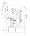
- FIG. 11 is a circuit schematic of a DC-DC converter with a control integrated circuit (IC) for regulating the DC-to-DC conversion according to one embodiment.
- the circuit 1100 may include a controller 1102 coupled to the bipolar junction transistor (BJT) 220 for regulating energy transfer of energy to a load, such as LEDs 214 .
- BJT bipolar junction transistor
- LEDs 214 are illustrated as a load for power consumption throughout this description, any load may be coupled to the circuit 1100 to receive regulated energy for consumption.
- an electromagnetic interference (EMI) prevention circuit 1114 may be coupled between the line voltage V IN input node 202 and the controller 1102 .
- the V IN input node 202 may receive a rectified alternating current (AC) input signal for operating the circuit 1100 .
- a snubber circuit 1112 may be coupled between the V IN node 202 and the controller 1102 .
- the controller 1102 may output signals through a drive (DRV) output to a base of the BJT 220 and a source (SRC) output to an emitter of the BJT 220 .
- Other inputs may be provided to the controller 1102 for controlling the controller 1102 from an external component through the CTRL 1 and CTRL 2 inputs.
- controller 1102 may be configured with an input to sense current at the V IN 202 node.
- the controller 1102 may include certain circuits described above for controlling operation of the BJT 220 , such as by dynamically adjusting a reverse recovery time period of the BJT 220 and maintaining an average current output to the LEDs 214 .
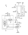
- FIG. 12 is a block diagram illustrating a dimmer system for a light-emitting diode (LED)-based bulb with two terminal drive of a bipolar junction transistor (BJT)-based power stage according to one embodiment of the disclosure.
- a system 1200 may include a dimmer compatibility circuit 1208 with a variable resistance device 1208 A and a control integrated circuit (IC) 1208 B.
- the dimmer compatibility circuit 1208 may couple an input stage having a dimmer 1204 and a rectifier 1206 with an output stage 1210 , which may include light emitting diodes (LEDs).
- the system 1200 may receive input from an AC mains line 1202 .
- the output stage 1210 may include a power stage based on a bipolar junction transistor (BJT) as described above.
- BJT bipolar junction transistor
- the output stage 1210 may include an emitter-switched bipolar junction transistor (BJT) in the configurations of FIG. 2 and FIG. 3 .
- FIG. 7 , FIG. 8 , and/or FIG. 10 may be stored as one or more instructions or code on a computer-readable medium. Examples include non-transitory computer-readable media encoded with a data structure and computer-readable media encoded with a computer program.
- Computer-readable media includes physical computer storage media. A storage medium may be any available medium that can be accessed by a computer.
- such computer-readable media can comprise random access memory (RAM), read-only memory (ROM), electrically erasable programmable read-only memory (EEPROM), compact-disc read-only memory (CD-ROM) or other optical disk storage, magnetic disk storage or other magnetic storage devices, or any other medium that can be used to store desired program code in the form of instructions or data structures and that can be accessed by a computer.
- Disk and disc includes compact discs (CD), laser discs, optical discs, digital versatile discs (DVD), floppy disks and blu-ray discs. Generally, disks reproduce data magnetically, and discs reproduce data optically. Combinations of the above should also be included within the scope of computer-readable media.
- instructions and/or data may be provided as signals on transmission media included in a communication apparatus.
- a communication apparatus may include a transceiver having signals indicative of instructions and data. The instructions and data are configured to cause one or more processors to implement the functions outlined in the claims.
Landscapes
- Engineering & Computer Science (AREA)
- Power Engineering (AREA)
- Circuit Arrangement For Electric Light Sources In General (AREA)
Abstract
Description
The waveforms of
where TTf is the switching cycle time, that is the duration of time from
I out
A larger difference between current values IPf and IP results from a larger transition turn-
The error compared to the desired peak current IP may then be calculated as:
VIN and Vddh may be measured by the
where VLOAD is a voltage across the
where the actual peak current, IPf, may be calculated as:
and the target peak current may be calculated as:
Thus, the amount of error δIP between the actual IPf and target IP value of peak collector current IC may be calculated as
In embodiments with a small value of IB, such as for certain BJTs with a large value of current gain β, the base current IB may be ignored from the error equation without affecting the correction significantly.
The target peak collector current after compensation, IPc, may then be calculated from:
I Pc =I P −δI P,
where IP is the desired peak current without compensation for the reverse recovery period and δIP is the calculated value from Tstg described above.
When no correction is applied, it may be assumed that T1RR=T1, and thus the error in the average output current value may be calculated as:
The computations described above apply to critical-conduction mode (CRM) of operation. Similar equations may be derived for discontinuous conduction mode (DCM) and continuous conduction mode (CCM).
By lowering the target peak current value IP to a compensated peak value IPc, a final inductor peak current value IPf matches the desired peak current value IP when the reverse recovery time period occurs. The effect of the compensation is shown in
If peak current Ipk increases by a delta δ due to the reverse recovery time period of the BJT, then the
Q pushed =[I pk(1+δ)][T2B(1+δ)].
I out,scaled =I out *k*(1−δ).
The scaled output current value described above in the
Claims (22)
Priority Applications (1)
| Application Number | Priority Date | Filing Date | Title |
|---|---|---|---|
| US14/341,984 US9504106B2 (en) | 2013-07-29 | 2014-07-28 | Compensating for a reverse recovery time period of a bipolar junction transistor (BJT) in switch-mode operation of a light-emitting diode (LED)-based bulb |
Applications Claiming Priority (2)
| Application Number | Priority Date | Filing Date | Title |
|---|---|---|---|
| US201361859638P | 2013-07-29 | 2013-07-29 | |
| US14/341,984 US9504106B2 (en) | 2013-07-29 | 2014-07-28 | Compensating for a reverse recovery time period of a bipolar junction transistor (BJT) in switch-mode operation of a light-emitting diode (LED)-based bulb |
Publications (2)
| Publication Number | Publication Date |
|---|---|
| US20150028768A1 US20150028768A1 (en) | 2015-01-29 |
| US9504106B2 true US9504106B2 (en) | 2016-11-22 |
Family
ID=52389915
Family Applications (1)
| Application Number | Title | Priority Date | Filing Date |
|---|---|---|---|
| US14/341,984 Active 2034-08-27 US9504106B2 (en) | 2013-07-29 | 2014-07-28 | Compensating for a reverse recovery time period of a bipolar junction transistor (BJT) in switch-mode operation of a light-emitting diode (LED)-based bulb |
Country Status (2)
| Country | Link |
|---|---|
| US (1) | US9504106B2 (en) |
| WO (1) | WO2015017315A1 (en) |
Cited By (1)
| Publication number | Priority date | Publication date | Assignee | Title |
|---|---|---|---|---|
| TWI897079B (en) * | 2022-11-02 | 2025-09-11 | 美商茂力科技股份有限公司 | Multi-mode power factor correction circuit and method for controlling the same |
Families Citing this family (8)
| Publication number | Priority date | Publication date | Assignee | Title |
|---|---|---|---|---|
| US20130320880A1 (en) * | 2012-05-16 | 2013-12-05 | James T. Walker | Rms responding voltage converter for led lights |
| US9520794B2 (en) * | 2012-07-25 | 2016-12-13 | Philips Lighting Holding B.V | Acceleration of output energy provision for a load during start-up of a switching power converter |
| US9253833B2 (en) * | 2013-05-17 | 2016-02-02 | Cirrus Logic, Inc. | Single pin control of bipolar junction transistor (BJT)-based power stage |
| US9413241B1 (en) * | 2015-01-15 | 2016-08-09 | Dialog Semiconductor Inc. | Self-powered BJT driver for power supplies |
| US9525333B1 (en) * | 2015-06-05 | 2016-12-20 | Power Integrations Limited | BJT driver with dynamic adjustment of storage time versus input line voltage variations |
| TWI728312B (en) * | 2019-02-13 | 2021-05-21 | 益力半導體股份有限公司 | Linear drive energy recovery system |
| CN113747635B (en) * | 2021-08-09 | 2024-05-03 | 厦门普为光电科技有限公司 | Dimming circuit |
| CN113747634B (en) * | 2021-08-09 | 2023-11-10 | 厦门普为光电科技有限公司 | Light modulator |
Citations (182)
| Publication number | Priority date | Publication date | Assignee | Title |
|---|---|---|---|---|
| US3660751A (en) | 1971-03-29 | 1972-05-02 | Collins Radio Co | Dc-dc regulated inverter employing pulse-width modulation with a constant volt-second sensing transformer |
| US3790878A (en) | 1971-12-22 | 1974-02-05 | Keithley Instruments | Switching regulator having improved control circuiting |
| US4322785A (en) | 1979-05-18 | 1982-03-30 | The General Electric Company Limited | Transistor switching circuit |
| US4339671A (en) | 1980-03-21 | 1982-07-13 | General Electric Company | Proportional base drive circuit |
| US4342956A (en) | 1980-12-23 | 1982-08-03 | General Electric Company | Proportional base drive circuit |
| US4399500A (en) | 1981-06-29 | 1983-08-16 | Bell Telephone Laboratories, Incorporated | Multimode base drive circuit for power switching transistor |
| US4410810A (en) | 1981-08-06 | 1983-10-18 | Gould Inc. | High speed transistor switching circuit |
| US4493017A (en) | 1983-01-24 | 1985-01-08 | Reliance Electric Company | Single drive transformer with regenerative winding for p.w.m. supply having alternately conducting power devices |
| US4585986A (en) | 1983-11-29 | 1986-04-29 | The United States Of America As Represented By The Department Of Energy | DC switching regulated power supply for driving an inductive load |
| US4629971A (en) | 1985-04-11 | 1986-12-16 | Mai Basic Four, Inc. | Switch mode converter and improved primary switch drive therefor |
| US4675547A (en) | 1985-03-28 | 1987-06-23 | Kollmorgen Technologies Corpn. | High power transistor base drive circuit |
| US4677366A (en) | 1986-05-12 | 1987-06-30 | Pioneer Research, Inc. | Unity power factor power supply |
| US4683529A (en) | 1986-11-12 | 1987-07-28 | Zytec Corporation | Switching power supply with automatic power factor correction |
| US4737658A (en) | 1985-08-05 | 1988-04-12 | Brown, Boveri & Cie Ag | Centralized control receiver |
| US4739462A (en) | 1984-12-26 | 1988-04-19 | Hughes Aircraft Company | Power supply with noise immune current sensing |
| US4937728A (en) | 1989-03-07 | 1990-06-26 | Rca Licensing Corporation | Switch-mode power supply with burst mode standby operation |
| US4940929A (en) | 1989-06-23 | 1990-07-10 | Apollo Computer, Inc. | AC to DC converter with unity power factor |
| US4970635A (en) | 1988-11-14 | 1990-11-13 | Sundstrand Corporation | Inverter with proportional base drive controlled by a current transformer |
| US4977366A (en) | 1988-10-07 | 1990-12-11 | Lucas Weinschel Inc. | High frequency power sensing device |
| US5001620A (en) | 1988-07-25 | 1991-03-19 | Astec International Limited | Power factor improvement |
| US5003454A (en) | 1990-01-09 | 1991-03-26 | North American Philips Corporation | Power supply with improved power factor correction |
| US5055746A (en) | 1990-08-13 | 1991-10-08 | Electronic Ballast Technology, Incorporated | Remote control of fluorescent lamp ballast using power flow interruption coding with means to maintain filament voltage substantially constant as the lamp voltage decreases |
| US5109185A (en) | 1989-09-29 | 1992-04-28 | Ball Newton E | Phase-controlled reversible power converter presenting a controllable counter emf to a source of an impressed voltage |
| US5173643A (en) | 1990-06-25 | 1992-12-22 | Lutron Electronics Co., Inc. | Circuit for dimming compact fluorescent lamps |
| EP0536535A1 (en) | 1991-09-09 | 1993-04-14 | Matsushita Electric Industrial Co., Ltd. | Discharge-lamp lighting apparatus |
| US5264780A (en) | 1992-08-10 | 1993-11-23 | International Business Machines Corporation | On time control and gain circuit |
| US5278490A (en) | 1990-09-04 | 1994-01-11 | California Institute Of Technology | One-cycle controlled switching circuit |
| US5383109A (en) | 1993-12-10 | 1995-01-17 | University Of Colorado | High power factor boost rectifier apparatus |
| EP0636889A1 (en) | 1993-07-30 | 1995-02-01 | AT&T Corp. | Current estimating circuit for switch mode power supply |
| US5424665A (en) | 1991-05-21 | 1995-06-13 | Consorzio Per La Ricerca Sulla Microelettronica Nel Mezzogiorno | Power transistor driving circuit |
| US5424932A (en) | 1993-01-05 | 1995-06-13 | Yokogawa Electric Corporation | Multi-output switching power supply having an improved secondary output circuit |
| US5430635A (en) | 1993-12-06 | 1995-07-04 | Bertonee, Inc. | High power factor electronic transformer system for gaseous discharge tubes |
| US5479333A (en) | 1994-04-25 | 1995-12-26 | Chrysler Corporation | Power supply start up booster circuit |
| US5481178A (en) | 1993-03-23 | 1996-01-02 | Linear Technology Corporation | Control circuit and method for maintaining high efficiency over broad current ranges in a switching regulator circuit |
| US5486781A (en) | 1993-01-27 | 1996-01-23 | Samsung Electronics Co., Ltd. | Base current-control circuit of an output transistor |
| US5565761A (en) | 1994-09-02 | 1996-10-15 | Micro Linear Corp | Synchronous switching cascade connected offline PFC-PWM combination power converter controller |
| US5638265A (en) | 1993-08-24 | 1997-06-10 | Gabor; George | Low line harmonic AC to DC power supply |
| US5691890A (en) | 1995-12-01 | 1997-11-25 | International Business Machines Corporation | Power supply with power factor correction circuit |
| US5747977A (en) | 1995-03-30 | 1998-05-05 | Micro Linear Corporation | Switching regulator having low power mode responsive to load power consumption |
| US5757635A (en) | 1995-12-28 | 1998-05-26 | Samsung Electronics Co., Ltd. | Power factor correction circuit and circuit therefor having sense-FET and boost converter control circuit |
| US5764039A (en) | 1995-11-15 | 1998-06-09 | Samsung Electronics Co., Ltd. | Power factor correction circuit having indirect input voltage sensing |
| US5783909A (en) | 1997-01-10 | 1998-07-21 | Relume Corporation | Maintaining LED luminous intensity |
| US5798635A (en) | 1996-06-20 | 1998-08-25 | Micro Linear Corporation | One pin error amplifier and switched soft-start for an eight pin PFC-PWM combination integrated circuit converter controller |
| US5808453A (en) | 1996-08-21 | 1998-09-15 | Siliconix Incorporated | Synchronous current sharing pulse width modulator |
| US5874725A (en) | 1994-10-06 | 1999-02-23 | Mitsubishi Denki Kabushiki Kaisha | Non-contact IC card with phase variation detector |
| US5960207A (en) | 1997-01-21 | 1999-09-28 | Dell Usa, L.P. | System and method for reducing power losses by gating an active power factor conversion process |
| US6043633A (en) | 1998-06-05 | 2000-03-28 | Systel Development & Industries | Power factor correction method and apparatus |
| US6084450A (en) | 1997-01-14 | 2000-07-04 | The Regents Of The University Of California | PWM controller with one cycle response |
| US6091233A (en) | 1999-01-14 | 2000-07-18 | Micro Linear Corporation | Interleaved zero current switching in a power factor correction boost converter |
| US6160724A (en) | 1999-10-26 | 2000-12-12 | International Business Machines Corporation | Boost doubler circuit wherein an AC bridge rectifier is not required |
| US6229292B1 (en) | 1999-02-12 | 2001-05-08 | Analog Devices, Inc. | Voltage regulator compensation circuit and method |
| US6259614B1 (en) | 1999-07-12 | 2001-07-10 | International Rectifier Corporation | Power factor correction control circuit |
| US6300723B1 (en) | 1998-07-29 | 2001-10-09 | Philips Electronics North America Corporation | Apparatus for power factor control |
| US6304473B1 (en) | 2000-06-02 | 2001-10-16 | Iwatt | Operating a power converter at optimal efficiency |
| WO2001084697A2 (en) | 2000-05-03 | 2001-11-08 | Intersil Corporation | Dc to dc converter method and circuitry |
| US6343026B1 (en) | 2000-11-09 | 2002-01-29 | Artesyn Technologies, Inc. | Current limit circuit for interleaved converters |
| US6356040B1 (en) | 1996-09-26 | 2002-03-12 | Robert Bosch Gmbh | Arrangement for determining the state of a high-pressure gas discharge lamp on switching-on |
| EP1213823A2 (en) | 2000-12-04 | 2002-06-12 | Sanken Electric Co., Ltd. | DC-to-DC converter |
| US20020082056A1 (en) | 2000-12-27 | 2002-06-27 | Tadao Mandai | Vibrator controlling circuit |
| US6445600B2 (en) | 1998-07-13 | 2002-09-03 | Ben-Gurion University Of The Negev Research & Development Authority | Modular structure of an apparatus for regulating the harmonics of current drawn from power lines by an electronic load |
| US6469484B2 (en) | 2000-12-13 | 2002-10-22 | Semiconductor Components Industries Llc | Power supply circuit and method thereof to detect demagnitization of the power supply |
| US6510995B2 (en) | 2001-03-16 | 2003-01-28 | Koninklijke Philips Electronics N.V. | RGB LED based light driver using microprocessor controlled AC distributed power system |
| EP1289107A2 (en) | 2001-08-31 | 2003-03-05 | Power Integrations, Inc. | Method and apparatus for trimming current limit and frequency to maintain a constant maximum power |
| US6531854B2 (en) | 2001-03-30 | 2003-03-11 | Champion Microelectronic Corp. | Power factor correction circuit arrangement |
| US20030090252A1 (en) | 2001-11-13 | 2003-05-15 | Intel Corporation | Method and semiconductor die with multiple phase power converter |
| US20030111969A1 (en) | 2001-01-12 | 2003-06-19 | Hirofumi Konishi | Ballast for a discharge lamp |
| US6583550B2 (en) | 2000-10-24 | 2003-06-24 | Toyoda Gosei Co., Ltd. | Fluorescent tube with light emitting diodes |
| US20030160576A1 (en) | 2001-06-08 | 2003-08-28 | Toshio Suzuki | Discharge lamp igniter device and projector device |
| US20030174520A1 (en) | 2000-10-24 | 2003-09-18 | Igor Bimbaud | Self-oscillating control circuit voltage converter |
| US6628106B1 (en) | 2001-07-30 | 2003-09-30 | University Of Central Florida | Control method and circuit to provide voltage and current regulation for multiphase DC/DC converters |
| US20030214821A1 (en) | 2002-05-16 | 2003-11-20 | Koninklijke Philips Electronics N.V. | System, method and apparatus for contact-less battery charging with dynamic control |
| US6657417B1 (en) | 2002-05-31 | 2003-12-02 | Champion Microelectronic Corp. | Power factor correction with carrier control and input voltage sensing |
| US20030223255A1 (en) | 2002-05-31 | 2003-12-04 | Green Power Technologies Ltd. | Method and apparatus for active power factor correction with minimum input current distortion |
| US6661182B2 (en) | 2002-04-03 | 2003-12-09 | Radionic Industries, Inc. | Lamp ballast system having improved power factor and end-of-lamp-life protection circuit |
| US6696803B2 (en) | 2000-12-14 | 2004-02-24 | Virginia Tech Intellectual Properties, Inc. | Self-oscillating electronic discharge lamp ballast with dimming control |
| US20040046683A1 (en) | 2001-03-08 | 2004-03-11 | Shindengen Electric Manufacturing Co., Ltd. | DC stabilized power supply |
| US6724174B1 (en) | 2002-09-12 | 2004-04-20 | Linear Technology Corp. | Adjustable minimum peak inductor current level for burst mode in current-mode DC-DC regulators |
| WO2004051834A1 (en) | 2002-11-27 | 2004-06-17 | Iwatt, Inc. | Digital regulation of power converters using primary-only feedback |
| US6758199B2 (en) | 2001-04-05 | 2004-07-06 | Mide Technology Corporation | Tuned power ignition system |
| US6768655B1 (en) | 2003-02-03 | 2004-07-27 | System General Corp. | Discontinuous mode PFC controller having a power saving modulator and operation method thereof |
| US6781351B2 (en) | 2002-08-17 | 2004-08-24 | Supertex Inc. | AC/DC cascaded power converters having high DC conversion ratio and improved AC line harmonics |
| US20040196672A1 (en) | 2003-02-03 | 2004-10-07 | Smk Corporation | Constant current output control method and constant current output control device for switching power supply circuit |
| US6839247B1 (en) | 2003-07-10 | 2005-01-04 | System General Corp. | PFC-PWM controller having a power saving means |
| US20050057237A1 (en) | 2002-01-11 | 2005-03-17 | Robert Clavel | Power factor controller |
| US6882552B2 (en) | 2000-06-02 | 2005-04-19 | Iwatt, Inc. | Power converter driven by power pulse and sense pulse |
| US6894471B2 (en) | 2002-05-31 | 2005-05-17 | St Microelectronics S.R.L. | Method of regulating the supply voltage of a load and related voltage regulator |
| US6933706B2 (en) | 2003-09-15 | 2005-08-23 | Semiconductor Components Industries, Llc | Method and circuit for optimizing power efficiency in a DC-DC converter |
| US6940733B2 (en) | 2002-08-22 | 2005-09-06 | Supertex, Inc. | Optimal control of wide conversion ratio switching converters |
| US6944034B1 (en) | 2003-06-30 | 2005-09-13 | Iwatt Inc. | System and method for input current shaping in a power converter |
| US20050207190A1 (en) | 2004-03-22 | 2005-09-22 | Gritter David J | Power system having a phase locked loop with a notch filter |
| US6956750B1 (en) | 2003-05-16 | 2005-10-18 | Iwatt Inc. | Power converter controller having event generator for detection of events and generation of digital error |
| US20050231183A1 (en) | 2004-04-16 | 2005-10-20 | Guojun Li | Driver with control interface facilitating use of the driver with varied DC-to-DC converter circuits |
| US20050270813A1 (en) | 2004-06-04 | 2005-12-08 | Wanfeng Zhang | Parallel current mode control |
| US6975523B2 (en) | 2002-10-16 | 2005-12-13 | Samsung Electronics Co., Ltd. | Power supply capable of protecting electric device circuit |
| US20050275354A1 (en) | 2004-06-10 | 2005-12-15 | Hausman Donald F Jr | Apparatus and methods for regulating delivery of electrical energy |
| US6980446B2 (en) | 2002-02-08 | 2005-12-27 | Sanken Electric Co., Ltd. | Circuit for starting power source apparatus |
| US20060013026A1 (en) | 2004-07-09 | 2006-01-19 | Infineon Technologies Ag | Method for driving a switch in a step-up converter and a drive circuit |
| US20060022648A1 (en) | 2004-08-02 | 2006-02-02 | Green Power Technologies Ltd. | Method and control circuitry for improved-performance switch-mode converters |
| WO2006022107A1 (en) | 2004-08-27 | 2006-03-02 | Sanken Electric Co., Ltd. | Power factor improving circuit |
| US7042161B1 (en) | 2005-02-28 | 2006-05-09 | Osram Sylvania, Inc. | Ballast with arc protection circuit |
| US7072191B2 (en) | 2002-04-26 | 2006-07-04 | Fdk Corporation | Switching power source circuit for independent per cycle control of ON/OFF time ratio |
| US7099163B1 (en) | 2005-11-14 | 2006-08-29 | Bcd Semiconductor Manufacturing Limited | PWM controller with constant output power limit for a power supply |
| US20060214603A1 (en) | 2005-03-22 | 2006-09-28 | In-Hwan Oh | Single-stage digital power converter for driving LEDs |
| WO2007016373A2 (en) | 2005-07-28 | 2007-02-08 | Synditec, Inc. | Pulsed current averaging controller with amplitude modulation and time division multiplexing for arrays of independent pluralities of light emitting diodes |
| US7221130B2 (en) | 2005-01-05 | 2007-05-22 | Fyrestorm, Inc. | Switching power converter employing pulse frequency modulation control |
| US7224206B2 (en) | 2004-02-24 | 2007-05-29 | Stmicroelectronics S.R.L. | Charge-pump with improved biasing of the body regions of the pass-transistors |
| US7233135B2 (en) | 2003-09-29 | 2007-06-19 | Murata Manufacturing Co., Ltd. | Ripple converter |
| US20070182347A1 (en) | 2006-01-20 | 2007-08-09 | Exclara Inc. | Impedance matching circuit for current regulation of solid state lighting |
| US7266001B1 (en) | 2004-03-19 | 2007-09-04 | Marvell International Ltd. | Method and apparatus for controlling power factor correction |
| US7292013B1 (en) | 2004-09-24 | 2007-11-06 | Marvell International Ltd. | Circuits, systems, methods, and software for power factor correction and/or control |
| US7295452B1 (en) | 2006-09-07 | 2007-11-13 | Green Mark Technology Inc. | Active power factor correction circuit and control method thereof |
| WO2008004008A2 (en) | 2006-07-07 | 2008-01-10 | Cambridge Semiconductor Limited | Switch mode power supply systems |
| US20080018261A1 (en) | 2006-05-01 | 2008-01-24 | Kastner Mark A | LED power supply with options for dimming |
| US20080043504A1 (en) | 2006-08-16 | 2008-02-21 | On-Bright Electronics (Shanghai) Co., Ltd. | System and method for providing control for switch-mode power supply |
| JP2008053181A (en) | 2006-08-28 | 2008-03-06 | Matsushita Electric Works Ltd | Dimmer |
| US20080062586A1 (en) | 2006-09-05 | 2008-03-13 | Silicon Laboratories, Inc. | Integrated circuit including a switching regulator design for power over Ethernet devices |
| US20080062584A1 (en) | 2005-01-14 | 2008-03-13 | Freitag James M | Method for manufacturing a magnetoresistive sensor having a novel junction structure for improved track width definition and pinned layer stability |
| US20080117656A1 (en) | 2006-11-20 | 2008-05-22 | Clarkin John P | Primary side sampled feedback control in power converters |
| US20080130336A1 (en) | 2005-07-01 | 2008-06-05 | Yasutaka Taguchi | Power Supply Device |
| US20080175029A1 (en) | 2007-01-18 | 2008-07-24 | Sang-Hwa Jung | Burst mode operation in a DC-DC converter |
| US7411379B2 (en) | 2004-12-21 | 2008-08-12 | Richtek Technology Corp. | Apparatus and method for over-voltage and over-current protection for a step-up current-mode converter |
| US7414371B1 (en) | 2005-11-21 | 2008-08-19 | Microsemi Corporation | Voltage regulation loop with variable gain control for inverter circuit |
| EP1962263A2 (en) | 2007-02-26 | 2008-08-27 | Samsung Electronics Co., Ltd. | Backlight unit, liquid crystal display device having the same and control method thereof |
| US7439810B2 (en) | 2006-06-08 | 2008-10-21 | Harris Corporation | Fast bias for power amplifier gating in a TDMA application |
| US20080259655A1 (en) | 2007-04-19 | 2008-10-23 | Da-Chun Wei | Switching-mode power converter and pulse-width-modulation control circuit with primary-side feedback control |
| US7449841B2 (en) | 2006-04-24 | 2008-11-11 | Microsemi Corp.—Analog Mixed Signal Group Ltd. | Charge limited high voltage switch circuits |
| US20080278132A1 (en) | 2007-05-07 | 2008-11-13 | Kesterson John W | Digital Compensation For Cable Drop In A Primary Side Control Power Supply Controller |
| WO2008152838A1 (en) | 2007-06-14 | 2008-12-18 | Sanken Electric Co., Ltd. | Ac-dc converter |
| US20080310194A1 (en) | 2007-06-13 | 2008-12-18 | Pei-Lun Huang | Method and apparatus for improving the light load efficiency of a switching mode converter |
| US20090040796A1 (en) | 2007-04-27 | 2009-02-12 | Cambridge Semiconductor Limited | Bipolar transistor drivers |
| US20090059632A1 (en) | 2007-08-28 | 2009-03-05 | Yong Li | System And Method For Controlling A Current Limit With Primary Side Sensing Using A Hybrid PWM and PFM Control |
| US20090108677A1 (en) | 2007-10-29 | 2009-04-30 | Linear Technology Corporation | Bidirectional power converters |
| US7554473B2 (en) | 2007-05-02 | 2009-06-30 | Cirrus Logic, Inc. | Control system using a nonlinear delta-sigma modulator with nonlinear process modeling |
| US20090184665A1 (en) | 2006-06-22 | 2009-07-23 | Alberto Ferro | Drive Device for Leds and Related Method |
| US7567091B2 (en) | 1998-05-22 | 2009-07-28 | Micron Technology, Inc. | Method for isolating a short-circuited integrated circuit (IC) from other ICs on a semiconductor wafer |
| US7606532B2 (en) | 2004-07-13 | 2009-10-20 | Stmicroelectronics S.A. | Adaptable power supply circuit |
| US20090295300A1 (en) | 2008-02-08 | 2009-12-03 | Purespectrum, Inc | Methods and apparatus for a dimmable ballast for use with led based light sources |
| WO2010011971A1 (en) | 2008-07-25 | 2010-01-28 | Cirrus Logic, Inc. | Switching power converter control with triac-based leading edge dimmer compatibility |
| US7667986B2 (en) | 2006-12-01 | 2010-02-23 | Flextronics International Usa, Inc. | Power system with power converters having an adaptive controller |
| US7684223B2 (en) | 2007-10-16 | 2010-03-23 | Hong Fu Jin Precision Industry (Shenzhen) Co., Ltd. | Automatic power supply converting circuit |
| US20100128501A1 (en) | 2008-10-21 | 2010-05-27 | On-Bright Electronics (Shanghai) Co., Ltd. | Systems and methods for constant voltage mode and constant current mode in flyback power converter with primary-side sensing and regulation |
| WO2010065598A2 (en) | 2008-12-07 | 2010-06-10 | Cirrus Logic, Inc. | Primary-side based control of secondary-side current for a transformer |
| US20100202165A1 (en) | 2007-09-28 | 2010-08-12 | Iwatt Inc. | Dynamic Drive of Switching Transistor of Switching Power Converter |
| US20100238689A1 (en) | 2009-03-20 | 2010-09-23 | Bcd Semiconductor Manufacturing Limited | Method and apparatus for controlling a constant current output in a switching mode power supply |
| US7804480B2 (en) | 2005-12-27 | 2010-09-28 | Lg Display Co., Ltd. | Hybrid backlight driving apparatus for liquid crystal display |
| EP2232949A2 (en) | 2008-01-16 | 2010-09-29 | Melexis NV | Improvements in and relating to low power lighting |
| US20100244793A1 (en) | 2009-03-27 | 2010-09-30 | Linear Technology Corporation | Average inductor current mode switching converters |
| US7834553B2 (en) | 2007-02-05 | 2010-11-16 | Vu1 Corporation | System and apparatus for cathodoluminescent lighting |
| EP2257124A1 (en) | 2009-05-29 | 2010-12-01 | Nxp B.V. | Circuit for connecting a low current lighting circuit to a dimmer |
| US7859488B2 (en) | 2005-08-12 | 2010-12-28 | Semiconductor Energy Laboratory Co., Ltd. | Semiconductor device, display device and electronic device equipped with the semiconductor device |
| US7872883B1 (en) | 2008-01-29 | 2011-01-18 | Fairchild Semiconductor Corporation | Synchronous buck power converter with free-running oscillator |
| WO2011008635A1 (en) | 2009-07-14 | 2011-01-20 | Iwatt Inc. | Adaptive dimmer detection and control for led lamp |
| US20110110132A1 (en) | 2009-11-12 | 2011-05-12 | Polar Semiconductor, Inc. | Time-limiting mode (tlm) for an interleaved power factor correction (pfc) converter |
| US20110199793A1 (en) | 2010-01-29 | 2011-08-18 | Naixing Kuang | Switching mode power supply with primary side control |
| US8008898B2 (en) | 2008-01-30 | 2011-08-30 | Cirrus Logic, Inc. | Switching regulator with boosted auxiliary winding supply |
| US20110276938A1 (en) | 2008-01-26 | 2011-11-10 | Jeffrey Robert Perry | Power supply optimization for electrical circuits designed over the internet |
| US20110291583A1 (en) | 2010-06-01 | 2011-12-01 | Feng-Min Shen | Dimmer circuit applicable for led device and control method thereof |
| US20110298442A1 (en) | 2010-06-04 | 2011-12-08 | Commissariat A I'energie Atomique Et Aux Energies Alternatives | Converter Circuit and Electronic System Comprising Such a Circuit |
| US20110309760A1 (en) | 2010-05-08 | 2011-12-22 | Robert Beland | LED Illumination systems |
| US20120062131A1 (en) | 2010-09-14 | 2012-03-15 | Choi Min-Soo | Method of driving a light source, light source apparatus for performing the method and display apparatus having the light source apparatus |
| US8169806B2 (en) | 2009-02-12 | 2012-05-01 | Apple Inc. | Power converter system with pulsed power transfer |
| US8193717B2 (en) | 2007-12-24 | 2012-06-05 | Lightech Electronic Industries Ltd. | Controller and method for controlling an intensity of a light emitting diode (LED) using a conventional AC dimmer |
| US20120146540A1 (en) | 2010-12-10 | 2012-06-14 | Khayat Joseph Maurice | Method and apparatus to control led brightness |
| US8222772B1 (en) | 2010-02-08 | 2012-07-17 | VI Chip, Inc. | Power supply system with power factor correction and efficient low power operation |
| US20120182003A1 (en) | 2011-01-14 | 2012-07-19 | Marco Flaibani | System and Method for Controlling a Switched-Mode Power Supply |
| US20120187997A1 (en) | 2010-07-29 | 2012-07-26 | Richtek Technology Corporation, R.O.C. | Circuit and method for providing absolute information for floating grounded integrated circuit |
| US8242764B2 (en) | 2008-09-12 | 2012-08-14 | Ricoh Company, Ltd. | DC-DC converter having VFM mode in which inductor current increases and switching frequency decreases |
| US8248145B2 (en) | 2009-06-30 | 2012-08-21 | Cirrus Logic, Inc. | Cascode configured switching using at least one low breakdown voltage internal, integrated circuit switch to control at least one high breakdown voltage external switch |
| US20120248998A1 (en) | 2011-03-30 | 2012-10-04 | Sanken Electric Co., Ltd. | Led driver and led illuminator having the same |
| US20120286843A1 (en) | 2011-05-11 | 2012-11-15 | Renesas Electronics Corporation | Protection circuit |
| US20120286686A1 (en) * | 2011-05-12 | 2012-11-15 | Panasonic Corporation | Lighting device for solid-state light source and illumination apparatus using same |
| US20120320640A1 (en) | 2011-06-15 | 2012-12-20 | Power Integrations, Inc. | Method and apparatus for programming a power converter controller with an external programming terminal having multiple functions |
| US8369109B2 (en) | 2006-11-09 | 2013-02-05 | Osram Gesellschaft Mit Beschrankter Haftung | Self-oscillating bipolar transistor DC/AC/DC converter using a pulse forming timer |
| US20130088902A1 (en) | 2011-10-11 | 2013-04-11 | Richard Alan Dunipace | Proportional bias switch driver circuit |
| US20130099694A1 (en) * | 2011-10-24 | 2013-04-25 | Panasonic Corporation | Lighting device and lighting fixture using the same |
| US20130107595A1 (en) | 2011-10-27 | 2013-05-02 | Stmicroelectronics (Tours) Sas | Control of a Switch in a Power Converter |
| US8441220B2 (en) | 2010-09-21 | 2013-05-14 | Denso Corporation | Control device for electric rotating machine |
| US20130181635A1 (en) | 2012-01-13 | 2013-07-18 | Texas Instruments Incorporated | LED Driver with Primary Side Sensing |
| US8536799B1 (en) | 2010-07-30 | 2013-09-17 | Cirrus Logic, Inc. | Dimmer detection |
| US8610364B2 (en) | 2010-07-30 | 2013-12-17 | Cirrus Logic, Inc. | Coordinated dimmer compatibility functions |
| US20140218978A1 (en) | 2013-02-01 | 2014-08-07 | Infineon Technologies Austria Ag | Converter with galvanic isolation |
| US8823283B2 (en) * | 2012-03-13 | 2014-09-02 | Dialog Semiconductor Inc. | Power dissipation monitor for current sink function of power switching transistor |
Family Cites Families (5)
| Publication number | Priority date | Publication date | Assignee | Title |
|---|---|---|---|---|
| US7276861B1 (en) * | 2004-09-21 | 2007-10-02 | Exclara, Inc. | System and method for driving LED |
| JP4564363B2 (en) * | 2005-01-13 | 2010-10-20 | パナソニック株式会社 | LED driving semiconductor device and LED driving device |
| US7071533B1 (en) * | 2005-02-04 | 2006-07-04 | Polar Semiconductor, Inc. | Bipolar junction transistor antifuse |
| US7880400B2 (en) * | 2007-09-21 | 2011-02-01 | Exclara, Inc. | Digital driver apparatus, method and system for solid state lighting |
| WO2012030867A2 (en) * | 2010-08-30 | 2012-03-08 | The Trustees Of Dartmouth College | High-efficiency base-driver circuit for power bipolar junction transistors |
-
2014
- 2014-07-28 US US14/341,984 patent/US9504106B2/en active Active
- 2014-07-28 WO PCT/US2014/048388 patent/WO2015017315A1/en not_active Ceased
Patent Citations (194)
| Publication number | Priority date | Publication date | Assignee | Title |
|---|---|---|---|---|
| US3660751A (en) | 1971-03-29 | 1972-05-02 | Collins Radio Co | Dc-dc regulated inverter employing pulse-width modulation with a constant volt-second sensing transformer |
| US3790878A (en) | 1971-12-22 | 1974-02-05 | Keithley Instruments | Switching regulator having improved control circuiting |
| US4322785A (en) | 1979-05-18 | 1982-03-30 | The General Electric Company Limited | Transistor switching circuit |
| US4339671A (en) | 1980-03-21 | 1982-07-13 | General Electric Company | Proportional base drive circuit |
| US4342956A (en) | 1980-12-23 | 1982-08-03 | General Electric Company | Proportional base drive circuit |
| US4399500A (en) | 1981-06-29 | 1983-08-16 | Bell Telephone Laboratories, Incorporated | Multimode base drive circuit for power switching transistor |
| US4410810A (en) | 1981-08-06 | 1983-10-18 | Gould Inc. | High speed transistor switching circuit |
| US4493017A (en) | 1983-01-24 | 1985-01-08 | Reliance Electric Company | Single drive transformer with regenerative winding for p.w.m. supply having alternately conducting power devices |
| US4585986A (en) | 1983-11-29 | 1986-04-29 | The United States Of America As Represented By The Department Of Energy | DC switching regulated power supply for driving an inductive load |
| US4739462A (en) | 1984-12-26 | 1988-04-19 | Hughes Aircraft Company | Power supply with noise immune current sensing |
| US4675547A (en) | 1985-03-28 | 1987-06-23 | Kollmorgen Technologies Corpn. | High power transistor base drive circuit |
| US4629971A (en) | 1985-04-11 | 1986-12-16 | Mai Basic Four, Inc. | Switch mode converter and improved primary switch drive therefor |
| US4737658A (en) | 1985-08-05 | 1988-04-12 | Brown, Boveri & Cie Ag | Centralized control receiver |
| US4677366A (en) | 1986-05-12 | 1987-06-30 | Pioneer Research, Inc. | Unity power factor power supply |
| US4683529A (en) | 1986-11-12 | 1987-07-28 | Zytec Corporation | Switching power supply with automatic power factor correction |
| US5001620A (en) | 1988-07-25 | 1991-03-19 | Astec International Limited | Power factor improvement |
| US4977366A (en) | 1988-10-07 | 1990-12-11 | Lucas Weinschel Inc. | High frequency power sensing device |
| US4970635A (en) | 1988-11-14 | 1990-11-13 | Sundstrand Corporation | Inverter with proportional base drive controlled by a current transformer |
| US4937728A (en) | 1989-03-07 | 1990-06-26 | Rca Licensing Corporation | Switch-mode power supply with burst mode standby operation |
| US4940929A (en) | 1989-06-23 | 1990-07-10 | Apollo Computer, Inc. | AC to DC converter with unity power factor |
| US5109185A (en) | 1989-09-29 | 1992-04-28 | Ball Newton E | Phase-controlled reversible power converter presenting a controllable counter emf to a source of an impressed voltage |
| US5003454A (en) | 1990-01-09 | 1991-03-26 | North American Philips Corporation | Power supply with improved power factor correction |
| US5173643A (en) | 1990-06-25 | 1992-12-22 | Lutron Electronics Co., Inc. | Circuit for dimming compact fluorescent lamps |
| US5055746A (en) | 1990-08-13 | 1991-10-08 | Electronic Ballast Technology, Incorporated | Remote control of fluorescent lamp ballast using power flow interruption coding with means to maintain filament voltage substantially constant as the lamp voltage decreases |
| US5278490A (en) | 1990-09-04 | 1994-01-11 | California Institute Of Technology | One-cycle controlled switching circuit |
| US5424665A (en) | 1991-05-21 | 1995-06-13 | Consorzio Per La Ricerca Sulla Microelettronica Nel Mezzogiorno | Power transistor driving circuit |
| EP0536535A1 (en) | 1991-09-09 | 1993-04-14 | Matsushita Electric Industrial Co., Ltd. | Discharge-lamp lighting apparatus |
| US5264780A (en) | 1992-08-10 | 1993-11-23 | International Business Machines Corporation | On time control and gain circuit |
| US5424932A (en) | 1993-01-05 | 1995-06-13 | Yokogawa Electric Corporation | Multi-output switching power supply having an improved secondary output circuit |
| US5486781A (en) | 1993-01-27 | 1996-01-23 | Samsung Electronics Co., Ltd. | Base current-control circuit of an output transistor |
| US6304066B1 (en) | 1993-03-23 | 2001-10-16 | Linear Technology Corporation | Control circuit and method for maintaining high efficiency over broad current ranges in a switching regular circuit |
| US6580258B2 (en) | 1993-03-23 | 2003-06-17 | Linear Technology Corporation | Control circuit and method for maintaining high efficiency over broad current ranges in a switching regulator circuit |
| US5994885A (en) | 1993-03-23 | 1999-11-30 | Linear Technology Corporation | Control circuit and method for maintaining high efficiency over broad current ranges in a switching regulator circuit |
| US5481178A (en) | 1993-03-23 | 1996-01-02 | Linear Technology Corporation | Control circuit and method for maintaining high efficiency over broad current ranges in a switching regulator circuit |
| EP0636889A1 (en) | 1993-07-30 | 1995-02-01 | AT&T Corp. | Current estimating circuit for switch mode power supply |
| US5638265A (en) | 1993-08-24 | 1997-06-10 | Gabor; George | Low line harmonic AC to DC power supply |
| US5430635A (en) | 1993-12-06 | 1995-07-04 | Bertonee, Inc. | High power factor electronic transformer system for gaseous discharge tubes |
| US5383109A (en) | 1993-12-10 | 1995-01-17 | University Of Colorado | High power factor boost rectifier apparatus |
| US5479333A (en) | 1994-04-25 | 1995-12-26 | Chrysler Corporation | Power supply start up booster circuit |
| US5565761A (en) | 1994-09-02 | 1996-10-15 | Micro Linear Corp | Synchronous switching cascade connected offline PFC-PWM combination power converter controller |
| US5874725A (en) | 1994-10-06 | 1999-02-23 | Mitsubishi Denki Kabushiki Kaisha | Non-contact IC card with phase variation detector |
| US5747977A (en) | 1995-03-30 | 1998-05-05 | Micro Linear Corporation | Switching regulator having low power mode responsive to load power consumption |
| US5764039A (en) | 1995-11-15 | 1998-06-09 | Samsung Electronics Co., Ltd. | Power factor correction circuit having indirect input voltage sensing |
| US5691890A (en) | 1995-12-01 | 1997-11-25 | International Business Machines Corporation | Power supply with power factor correction circuit |
| US5757635A (en) | 1995-12-28 | 1998-05-26 | Samsung Electronics Co., Ltd. | Power factor correction circuit and circuit therefor having sense-FET and boost converter control circuit |
| US5798635A (en) | 1996-06-20 | 1998-08-25 | Micro Linear Corporation | One pin error amplifier and switched soft-start for an eight pin PFC-PWM combination integrated circuit converter controller |
| US5808453A (en) | 1996-08-21 | 1998-09-15 | Siliconix Incorporated | Synchronous current sharing pulse width modulator |
| US6356040B1 (en) | 1996-09-26 | 2002-03-12 | Robert Bosch Gmbh | Arrangement for determining the state of a high-pressure gas discharge lamp on switching-on |
| US5783909A (en) | 1997-01-10 | 1998-07-21 | Relume Corporation | Maintaining LED luminous intensity |
| US6084450A (en) | 1997-01-14 | 2000-07-04 | The Regents Of The University Of California | PWM controller with one cycle response |
| US5960207A (en) | 1997-01-21 | 1999-09-28 | Dell Usa, L.P. | System and method for reducing power losses by gating an active power factor conversion process |
| US7567091B2 (en) | 1998-05-22 | 2009-07-28 | Micron Technology, Inc. | Method for isolating a short-circuited integrated circuit (IC) from other ICs on a semiconductor wafer |
| US6043633A (en) | 1998-06-05 | 2000-03-28 | Systel Development & Industries | Power factor correction method and apparatus |
| US6445600B2 (en) | 1998-07-13 | 2002-09-03 | Ben-Gurion University Of The Negev Research & Development Authority | Modular structure of an apparatus for regulating the harmonics of current drawn from power lines by an electronic load |
| US6300723B1 (en) | 1998-07-29 | 2001-10-09 | Philips Electronics North America Corporation | Apparatus for power factor control |
| US6091233A (en) | 1999-01-14 | 2000-07-18 | Micro Linear Corporation | Interleaved zero current switching in a power factor correction boost converter |
| US6229292B1 (en) | 1999-02-12 | 2001-05-08 | Analog Devices, Inc. | Voltage regulator compensation circuit and method |
| US6259614B1 (en) | 1999-07-12 | 2001-07-10 | International Rectifier Corporation | Power factor correction control circuit |
| US6160724A (en) | 1999-10-26 | 2000-12-12 | International Business Machines Corporation | Boost doubler circuit wherein an AC bridge rectifier is not required |
| WO2001084697A2 (en) | 2000-05-03 | 2001-11-08 | Intersil Corporation | Dc to dc converter method and circuitry |
| US6304473B1 (en) | 2000-06-02 | 2001-10-16 | Iwatt | Operating a power converter at optimal efficiency |
| US6882552B2 (en) | 2000-06-02 | 2005-04-19 | Iwatt, Inc. | Power converter driven by power pulse and sense pulse |
| US6583550B2 (en) | 2000-10-24 | 2003-06-24 | Toyoda Gosei Co., Ltd. | Fluorescent tube with light emitting diodes |
| US20030174520A1 (en) | 2000-10-24 | 2003-09-18 | Igor Bimbaud | Self-oscillating control circuit voltage converter |
| US6343026B1 (en) | 2000-11-09 | 2002-01-29 | Artesyn Technologies, Inc. | Current limit circuit for interleaved converters |
| EP1213823A2 (en) | 2000-12-04 | 2002-06-12 | Sanken Electric Co., Ltd. | DC-to-DC converter |
| US6469484B2 (en) | 2000-12-13 | 2002-10-22 | Semiconductor Components Industries Llc | Power supply circuit and method thereof to detect demagnitization of the power supply |
| US6696803B2 (en) | 2000-12-14 | 2004-02-24 | Virginia Tech Intellectual Properties, Inc. | Self-oscillating electronic discharge lamp ballast with dimming control |
| US20020082056A1 (en) | 2000-12-27 | 2002-06-27 | Tadao Mandai | Vibrator controlling circuit |
| US20030111969A1 (en) | 2001-01-12 | 2003-06-19 | Hirofumi Konishi | Ballast for a discharge lamp |
| US20040046683A1 (en) | 2001-03-08 | 2004-03-11 | Shindengen Electric Manufacturing Co., Ltd. | DC stabilized power supply |
| US6510995B2 (en) | 2001-03-16 | 2003-01-28 | Koninklijke Philips Electronics N.V. | RGB LED based light driver using microprocessor controlled AC distributed power system |
| US6531854B2 (en) | 2001-03-30 | 2003-03-11 | Champion Microelectronic Corp. | Power factor correction circuit arrangement |
| US6758199B2 (en) | 2001-04-05 | 2004-07-06 | Mide Technology Corporation | Tuned power ignition system |
| US20030160576A1 (en) | 2001-06-08 | 2003-08-28 | Toshio Suzuki | Discharge lamp igniter device and projector device |
| US6628106B1 (en) | 2001-07-30 | 2003-09-30 | University Of Central Florida | Control method and circuit to provide voltage and current regulation for multiphase DC/DC converters |
| EP1289107A2 (en) | 2001-08-31 | 2003-03-05 | Power Integrations, Inc. | Method and apparatus for trimming current limit and frequency to maintain a constant maximum power |
| US20030090252A1 (en) | 2001-11-13 | 2003-05-15 | Intel Corporation | Method and semiconductor die with multiple phase power converter |
| US20050057237A1 (en) | 2002-01-11 | 2005-03-17 | Robert Clavel | Power factor controller |
| US6980446B2 (en) | 2002-02-08 | 2005-12-27 | Sanken Electric Co., Ltd. | Circuit for starting power source apparatus |
| US6661182B2 (en) | 2002-04-03 | 2003-12-09 | Radionic Industries, Inc. | Lamp ballast system having improved power factor and end-of-lamp-life protection circuit |
| US7072191B2 (en) | 2002-04-26 | 2006-07-04 | Fdk Corporation | Switching power source circuit for independent per cycle control of ON/OFF time ratio |
| US20030214821A1 (en) | 2002-05-16 | 2003-11-20 | Koninklijke Philips Electronics N.V. | System, method and apparatus for contact-less battery charging with dynamic control |
| US20030223255A1 (en) | 2002-05-31 | 2003-12-04 | Green Power Technologies Ltd. | Method and apparatus for active power factor correction with minimum input current distortion |
| US6894471B2 (en) | 2002-05-31 | 2005-05-17 | St Microelectronics S.R.L. | Method of regulating the supply voltage of a load and related voltage regulator |
| US6657417B1 (en) | 2002-05-31 | 2003-12-02 | Champion Microelectronic Corp. | Power factor correction with carrier control and input voltage sensing |
| US6781351B2 (en) | 2002-08-17 | 2004-08-24 | Supertex Inc. | AC/DC cascaded power converters having high DC conversion ratio and improved AC line harmonics |
| US6940733B2 (en) | 2002-08-22 | 2005-09-06 | Supertex, Inc. | Optimal control of wide conversion ratio switching converters |
| US6724174B1 (en) | 2002-09-12 | 2004-04-20 | Linear Technology Corp. | Adjustable minimum peak inductor current level for burst mode in current-mode DC-DC regulators |
| US6975523B2 (en) | 2002-10-16 | 2005-12-13 | Samsung Electronics Co., Ltd. | Power supply capable of protecting electric device circuit |
| WO2004051834A1 (en) | 2002-11-27 | 2004-06-17 | Iwatt, Inc. | Digital regulation of power converters using primary-only feedback |
| US6768655B1 (en) | 2003-02-03 | 2004-07-27 | System General Corp. | Discontinuous mode PFC controller having a power saving modulator and operation method thereof |
| US20040196672A1 (en) | 2003-02-03 | 2004-10-07 | Smk Corporation | Constant current output control method and constant current output control device for switching power supply circuit |
| US6956750B1 (en) | 2003-05-16 | 2005-10-18 | Iwatt Inc. | Power converter controller having event generator for detection of events and generation of digital error |
| US6944034B1 (en) | 2003-06-30 | 2005-09-13 | Iwatt Inc. | System and method for input current shaping in a power converter |
| US7161816B2 (en) | 2003-06-30 | 2007-01-09 | Iwatt Inc. | System and method for input current shaping in a power converter |
| US6839247B1 (en) | 2003-07-10 | 2005-01-04 | System General Corp. | PFC-PWM controller having a power saving means |
| US6933706B2 (en) | 2003-09-15 | 2005-08-23 | Semiconductor Components Industries, Llc | Method and circuit for optimizing power efficiency in a DC-DC converter |
| US7233135B2 (en) | 2003-09-29 | 2007-06-19 | Murata Manufacturing Co., Ltd. | Ripple converter |
| US7224206B2 (en) | 2004-02-24 | 2007-05-29 | Stmicroelectronics S.R.L. | Charge-pump with improved biasing of the body regions of the pass-transistors |
| US7266001B1 (en) | 2004-03-19 | 2007-09-04 | Marvell International Ltd. | Method and apparatus for controlling power factor correction |
| US20050207190A1 (en) | 2004-03-22 | 2005-09-22 | Gritter David J | Power system having a phase locked loop with a notch filter |
| US20050231183A1 (en) | 2004-04-16 | 2005-10-20 | Guojun Li | Driver with control interface facilitating use of the driver with varied DC-to-DC converter circuits |
| US20050270813A1 (en) | 2004-06-04 | 2005-12-08 | Wanfeng Zhang | Parallel current mode control |
| US20050275354A1 (en) | 2004-06-10 | 2005-12-15 | Hausman Donald F Jr | Apparatus and methods for regulating delivery of electrical energy |
| US20060013026A1 (en) | 2004-07-09 | 2006-01-19 | Infineon Technologies Ag | Method for driving a switch in a step-up converter and a drive circuit |
| US7606532B2 (en) | 2004-07-13 | 2009-10-20 | Stmicroelectronics S.A. | Adaptable power supply circuit |
| US20060022648A1 (en) | 2004-08-02 | 2006-02-02 | Green Power Technologies Ltd. | Method and control circuitry for improved-performance switch-mode converters |
| WO2006013557A2 (en) | 2004-08-02 | 2006-02-09 | Green Power Technologies Ltd. | Method and control circuitry for improved-performance switch-mode converters |
| US20070103949A1 (en) | 2004-08-27 | 2007-05-10 | Sanken Electric Co., Ltd. | Power factor improving circuit |
| WO2006022107A1 (en) | 2004-08-27 | 2006-03-02 | Sanken Electric Co., Ltd. | Power factor improving circuit |
| US7292013B1 (en) | 2004-09-24 | 2007-11-06 | Marvell International Ltd. | Circuits, systems, methods, and software for power factor correction and/or control |
| US7411379B2 (en) | 2004-12-21 | 2008-08-12 | Richtek Technology Corp. | Apparatus and method for over-voltage and over-current protection for a step-up current-mode converter |
| US7221130B2 (en) | 2005-01-05 | 2007-05-22 | Fyrestorm, Inc. | Switching power converter employing pulse frequency modulation control |
| US20080062584A1 (en) | 2005-01-14 | 2008-03-13 | Freitag James M | Method for manufacturing a magnetoresistive sensor having a novel junction structure for improved track width definition and pinned layer stability |
| US7042161B1 (en) | 2005-02-28 | 2006-05-09 | Osram Sylvania, Inc. | Ballast with arc protection circuit |
| US20060214603A1 (en) | 2005-03-22 | 2006-09-28 | In-Hwan Oh | Single-stage digital power converter for driving LEDs |
| US20080130336A1 (en) | 2005-07-01 | 2008-06-05 | Yasutaka Taguchi | Power Supply Device |
| WO2007016373A2 (en) | 2005-07-28 | 2007-02-08 | Synditec, Inc. | Pulsed current averaging controller with amplitude modulation and time division multiplexing for arrays of independent pluralities of light emitting diodes |
| US7859488B2 (en) | 2005-08-12 | 2010-12-28 | Semiconductor Energy Laboratory Co., Ltd. | Semiconductor device, display device and electronic device equipped with the semiconductor device |
| US7099163B1 (en) | 2005-11-14 | 2006-08-29 | Bcd Semiconductor Manufacturing Limited | PWM controller with constant output power limit for a power supply |
| US7414371B1 (en) | 2005-11-21 | 2008-08-19 | Microsemi Corporation | Voltage regulation loop with variable gain control for inverter circuit |
| US7804480B2 (en) | 2005-12-27 | 2010-09-28 | Lg Display Co., Ltd. | Hybrid backlight driving apparatus for liquid crystal display |
| US20070182347A1 (en) | 2006-01-20 | 2007-08-09 | Exclara Inc. | Impedance matching circuit for current regulation of solid state lighting |
| US7449841B2 (en) | 2006-04-24 | 2008-11-11 | Microsemi Corp.—Analog Mixed Signal Group Ltd. | Charge limited high voltage switch circuits |
| US20080018261A1 (en) | 2006-05-01 | 2008-01-24 | Kastner Mark A | LED power supply with options for dimming |
| US7439810B2 (en) | 2006-06-08 | 2008-10-21 | Harris Corporation | Fast bias for power amplifier gating in a TDMA application |
| US20090184665A1 (en) | 2006-06-22 | 2009-07-23 | Alberto Ferro | Drive Device for Leds and Related Method |
| WO2008004008A2 (en) | 2006-07-07 | 2008-01-10 | Cambridge Semiconductor Limited | Switch mode power supply systems |
| US20090067204A1 (en) | 2006-08-16 | 2009-03-12 | On-Bright Electronics (Shanghai ) Co., Ltd. | System and method for providing control for switch-mode power supply |
| US20080043504A1 (en) | 2006-08-16 | 2008-02-21 | On-Bright Electronics (Shanghai) Co., Ltd. | System and method for providing control for switch-mode power supply |
| JP2008053181A (en) | 2006-08-28 | 2008-03-06 | Matsushita Electric Works Ltd | Dimmer |
| US20080062586A1 (en) | 2006-09-05 | 2008-03-13 | Silicon Laboratories, Inc. | Integrated circuit including a switching regulator design for power over Ethernet devices |
| US7295452B1 (en) | 2006-09-07 | 2007-11-13 | Green Mark Technology Inc. | Active power factor correction circuit and control method thereof |
| US8369109B2 (en) | 2006-11-09 | 2013-02-05 | Osram Gesellschaft Mit Beschrankter Haftung | Self-oscillating bipolar transistor DC/AC/DC converter using a pulse forming timer |
| US20080117656A1 (en) | 2006-11-20 | 2008-05-22 | Clarkin John P | Primary side sampled feedback control in power converters |
| US7667986B2 (en) | 2006-12-01 | 2010-02-23 | Flextronics International Usa, Inc. | Power system with power converters having an adaptive controller |
| US20080175029A1 (en) | 2007-01-18 | 2008-07-24 | Sang-Hwa Jung | Burst mode operation in a DC-DC converter |
| US7834553B2 (en) | 2007-02-05 | 2010-11-16 | Vu1 Corporation | System and apparatus for cathodoluminescent lighting |
| EP1962263A2 (en) | 2007-02-26 | 2008-08-27 | Samsung Electronics Co., Ltd. | Backlight unit, liquid crystal display device having the same and control method thereof |
| US20080259655A1 (en) | 2007-04-19 | 2008-10-23 | Da-Chun Wei | Switching-mode power converter and pulse-width-modulation control circuit with primary-side feedback control |
| US20090040796A1 (en) | 2007-04-27 | 2009-02-12 | Cambridge Semiconductor Limited | Bipolar transistor drivers |
| US7719246B2 (en) | 2007-05-02 | 2010-05-18 | Cirrus Logic, Inc. | Power control system using a nonlinear delta-sigma modulator with nonlinear power conversion process modeling |
| US7746043B2 (en) | 2007-05-02 | 2010-06-29 | Cirrus Logic, Inc. | Inductor flyback detection using switch gate change characteristic detection |
| US7554473B2 (en) | 2007-05-02 | 2009-06-30 | Cirrus Logic, Inc. | Control system using a nonlinear delta-sigma modulator with nonlinear process modeling |
| US7894216B2 (en) | 2007-05-02 | 2011-02-22 | Cirrus Logic, Inc. | Switching power converter with efficient switching control signal period generation |
| US7719248B1 (en) | 2007-05-02 | 2010-05-18 | Cirrus Logic, Inc. | Discontinuous conduction mode (DCM) using sensed current for a switch-mode converter |
| US20080278132A1 (en) | 2007-05-07 | 2008-11-13 | Kesterson John W | Digital Compensation For Cable Drop In A Primary Side Control Power Supply Controller |
| US20080310194A1 (en) | 2007-06-13 | 2008-12-18 | Pei-Lun Huang | Method and apparatus for improving the light load efficiency of a switching mode converter |
| WO2008152838A1 (en) | 2007-06-14 | 2008-12-18 | Sanken Electric Co., Ltd. | Ac-dc converter |
| US20090059632A1 (en) | 2007-08-28 | 2009-03-05 | Yong Li | System And Method For Controlling A Current Limit With Primary Side Sensing Using A Hybrid PWM and PFM Control |
| US20130279209A1 (en) * | 2007-09-28 | 2013-10-24 | Iwatt Inc. | Dynamic drive of switching transistor of switching power converter |
| US20100202165A1 (en) | 2007-09-28 | 2010-08-12 | Iwatt Inc. | Dynamic Drive of Switching Transistor of Switching Power Converter |
| US7684223B2 (en) | 2007-10-16 | 2010-03-23 | Hong Fu Jin Precision Industry (Shenzhen) Co., Ltd. | Automatic power supply converting circuit |
| US20090108677A1 (en) | 2007-10-29 | 2009-04-30 | Linear Technology Corporation | Bidirectional power converters |
| US8193717B2 (en) | 2007-12-24 | 2012-06-05 | Lightech Electronic Industries Ltd. | Controller and method for controlling an intensity of a light emitting diode (LED) using a conventional AC dimmer |
| EP2232949A2 (en) | 2008-01-16 | 2010-09-29 | Melexis NV | Improvements in and relating to low power lighting |
| US20110276938A1 (en) | 2008-01-26 | 2011-11-10 | Jeffrey Robert Perry | Power supply optimization for electrical circuits designed over the internet |
| US7872883B1 (en) | 2008-01-29 | 2011-01-18 | Fairchild Semiconductor Corporation | Synchronous buck power converter with free-running oscillator |
| US8008898B2 (en) | 2008-01-30 | 2011-08-30 | Cirrus Logic, Inc. | Switching regulator with boosted auxiliary winding supply |
| US20090295300A1 (en) | 2008-02-08 | 2009-12-03 | Purespectrum, Inc | Methods and apparatus for a dimmable ballast for use with led based light sources |
| WO2010011971A1 (en) | 2008-07-25 | 2010-01-28 | Cirrus Logic, Inc. | Switching power converter control with triac-based leading edge dimmer compatibility |
| US8242764B2 (en) | 2008-09-12 | 2012-08-14 | Ricoh Company, Ltd. | DC-DC converter having VFM mode in which inductor current increases and switching frequency decreases |
| US20100128501A1 (en) | 2008-10-21 | 2010-05-27 | On-Bright Electronics (Shanghai) Co., Ltd. | Systems and methods for constant voltage mode and constant current mode in flyback power converter with primary-side sensing and regulation |
| WO2010065598A2 (en) | 2008-12-07 | 2010-06-10 | Cirrus Logic, Inc. | Primary-side based control of secondary-side current for a transformer |
| US8169806B2 (en) | 2009-02-12 | 2012-05-01 | Apple Inc. | Power converter system with pulsed power transfer |
| US20100238689A1 (en) | 2009-03-20 | 2010-09-23 | Bcd Semiconductor Manufacturing Limited | Method and apparatus for controlling a constant current output in a switching mode power supply |
| US20100244793A1 (en) | 2009-03-27 | 2010-09-30 | Linear Technology Corporation | Average inductor current mode switching converters |
| EP2257124A1 (en) | 2009-05-29 | 2010-12-01 | Nxp B.V. | Circuit for connecting a low current lighting circuit to a dimmer |
| US8248145B2 (en) | 2009-06-30 | 2012-08-21 | Cirrus Logic, Inc. | Cascode configured switching using at least one low breakdown voltage internal, integrated circuit switch to control at least one high breakdown voltage external switch |
| WO2011008635A1 (en) | 2009-07-14 | 2011-01-20 | Iwatt Inc. | Adaptive dimmer detection and control for led lamp |
| US20110110132A1 (en) | 2009-11-12 | 2011-05-12 | Polar Semiconductor, Inc. | Time-limiting mode (tlm) for an interleaved power factor correction (pfc) converter |
| US20110199793A1 (en) | 2010-01-29 | 2011-08-18 | Naixing Kuang | Switching mode power supply with primary side control |
| US8222772B1 (en) | 2010-02-08 | 2012-07-17 | VI Chip, Inc. | Power supply system with power factor correction and efficient low power operation |
| US20110309760A1 (en) | 2010-05-08 | 2011-12-22 | Robert Beland | LED Illumination systems |
| US20110291583A1 (en) | 2010-06-01 | 2011-12-01 | Feng-Min Shen | Dimmer circuit applicable for led device and control method thereof |
| US20110298442A1 (en) | 2010-06-04 | 2011-12-08 | Commissariat A I'energie Atomique Et Aux Energies Alternatives | Converter Circuit and Electronic System Comprising Such a Circuit |
| US20120187997A1 (en) | 2010-07-29 | 2012-07-26 | Richtek Technology Corporation, R.O.C. | Circuit and method for providing absolute information for floating grounded integrated circuit |
| US8536799B1 (en) | 2010-07-30 | 2013-09-17 | Cirrus Logic, Inc. | Dimmer detection |
| US8610364B2 (en) | 2010-07-30 | 2013-12-17 | Cirrus Logic, Inc. | Coordinated dimmer compatibility functions |
| US20120062131A1 (en) | 2010-09-14 | 2012-03-15 | Choi Min-Soo | Method of driving a light source, light source apparatus for performing the method and display apparatus having the light source apparatus |
| US8441220B2 (en) | 2010-09-21 | 2013-05-14 | Denso Corporation | Control device for electric rotating machine |
| US20120146540A1 (en) | 2010-12-10 | 2012-06-14 | Khayat Joseph Maurice | Method and apparatus to control led brightness |
| US20120182003A1 (en) | 2011-01-14 | 2012-07-19 | Marco Flaibani | System and Method for Controlling a Switched-Mode Power Supply |
| US20120248998A1 (en) | 2011-03-30 | 2012-10-04 | Sanken Electric Co., Ltd. | Led driver and led illuminator having the same |
| US20120286843A1 (en) | 2011-05-11 | 2012-11-15 | Renesas Electronics Corporation | Protection circuit |
| US20120286686A1 (en) * | 2011-05-12 | 2012-11-15 | Panasonic Corporation | Lighting device for solid-state light source and illumination apparatus using same |
| US20120320640A1 (en) | 2011-06-15 | 2012-12-20 | Power Integrations, Inc. | Method and apparatus for programming a power converter controller with an external programming terminal having multiple functions |
| US20130088902A1 (en) | 2011-10-11 | 2013-04-11 | Richard Alan Dunipace | Proportional bias switch driver circuit |
| US20130099694A1 (en) * | 2011-10-24 | 2013-04-25 | Panasonic Corporation | Lighting device and lighting fixture using the same |
| US20130107595A1 (en) | 2011-10-27 | 2013-05-02 | Stmicroelectronics (Tours) Sas | Control of a Switch in a Power Converter |
| US20130181635A1 (en) | 2012-01-13 | 2013-07-18 | Texas Instruments Incorporated | LED Driver with Primary Side Sensing |
| US8823283B2 (en) * | 2012-03-13 | 2014-09-02 | Dialog Semiconductor Inc. | Power dissipation monitor for current sink function of power switching transistor |
| US20140218978A1 (en) | 2013-02-01 | 2014-08-07 | Infineon Technologies Austria Ag | Converter with galvanic isolation |
Non-Patent Citations (92)
| Title |
|---|
| Avant et al., "Analysis of magnetic proportional drive circuits for bipolar junction transistors" PESC 1985, pp. 375-381. |
| Balogh, Laszlo, et al, Power-Factor Correction with Interleaved Boost Converters in Continuous-Inductr-Current Mode, 1993, IEEE, pp. 168-174, Switzerland. |
| Bell, David, "Designing optimal base drive for high voltage switching transistors", Proceeding of PowerCon7, 1980. |
| Ben-Yaakov, et al, The Dynamics of a PWM Boost Converter with Resistive Input, IEEE Transactions on Industrial Electronics, vol. 46., No. 3, Jun. 1999, pp. 1-8, Negev, Beer-Sheva, Israel. |
| Brown, et al, PFC Converter Design with IR1150 One Cycle Control IC, International Rectifier, Application Note AN-1 077, pp. 1-18, El Segundo CA, USA. |
| Cheng, Hung L., et al, A Novel Single-Stage High-Power-Factor Electronic Ballast with Symmetrical Topology, Power Electronics and Motion Control Conference, 2006. IPEMEC 2006. CES/IEEE 5th International, Aug. 14-16, 2006, vol. 50, No. 4, Aug. 2003, pp. 759-766, Nat. Ilan Univ., Taiwan. |
| Erickson, Robert W., et al, Fundamentals of Power Electronics, Second Edition, Chapter 6, 2001, pp. 131-184, Boulder CO, USA. |
| Fairchild Semicondctor, Simple Ballast Controller, KA7541, Rev. 1.0.3, Sep. 27, 2001, pp. 1-14, San Jose, CA, USA. |
| Fairchild Semiconductor, 500W Power-Factor-Corrected (PFC) Converter Design with FAN4810, Application Note 6004, Rev. 1.0.1, Oct. 31, 2003, pp. 1-14, San Jose, CA, USA. |
| Fairchild Semiconductor, Ballast Control IC FAN7532, Rev. 1.0.3, Jun. 2006, pp. 1-16, San Jose, California, USA. |
| Fairchild Semiconductor, Ballast Control IC, FAN 7711, Rev. 1.0.3, 2007, pp. 1-23, San Jose, California, USA. |
| Fairchild Semiconductor, Design of Power Factor Correction Circuit Using FAN7527B, Application Note AN4121, Rev. 1.0.1, May 30, 2002, pp. 1-12, San Jose, CA, USA. |
| Fairchild Semiconductor, Low Start-Up Current PFC/PWM Controller Combos FAN4800, Rev. 1.0.6, Nov. 2006, pp. 1-20, San Jose, CA, USA. |
| Fairchild Semiconductor, Power Factor Controller, ML4812, Rev. 1.0.4, May 31, 2001, pp. 1-18, San Jose, CA, USA. |
| Fairchild Semiconductor, Power Factor Correction Controller FAN7527B, Aug. 16, 2003, pp. 1-12, San Jose, CA, USA. |
| Fairchild Semiconductor, Simple Ballast Controller, FAN7544, Rev. 1.0.0, Sep. 21, 2004, pp. 1-14, San Jose, California, USA. |
| Fairchild Semiconductor, ZVS Average Current PFC Controller FAN 4822, Rev. 1.0.1, Aug. 10, 2001, pp. 1-10, San Jose, CA, USA. |
| Fairchild Semiconductor. Theory and Application of the ML4821 Average Current Mode PFC Controllerr, Fairchild Semiconductor Application Note 42030. Rev. 1.0, Oct. 25, 2000, pp. 1-19, San Jose, California, USA. |
| Fairfield Semiconductor, Power Factor Correction (PFC) Basics, Application Note 42047, Rev. 0.9.0, Aug. 19, 2004, pp. 1-11, San Jose, CA, USA. |
| Freescale Semiconductor, Design of Indirect Power Factor Correction Using 56F800/E, Freescale Semiconductor Application Note, AN1965, Rev. 1, Jul. 2005, pp. 1-20, Chandler, AZ, USA. |
| Freescale Semiconductor, Dimmable Light Ballast with Power Factor Correction, Designer Reference Manual, DRM067, Rev. 1, Dec. 2005, M68HC08 Microcontrollers, pp. 1-72, Chandler, AZ, USA. |
| Freescale Semiconductor, Implementing PFC Average Current Mode Control using the MC9S12E128, Application Note AN3052, Addendum to Reference Design Manual DRM064, Rev. 0, Nov. 2005, pp. 1-8, Chandler, AZ, USA. |
| Garcia, 0., et al, High Efficiency PFC Converter to Meet EN610000302 and A14, Industrial Electronics, 2002. ISIE 2002. Proceedings of the 2002 IEEE International Symposium, vol. 3, pp. 975-980, Div. de Ingenieria Electronica, Univ. Politecnica de Madrid, Spain. |
| Hirota, et al, Analysis of Single Switch Delta-Sigma Modulated Pulse Space Modulation PFC Converter Effectively Using Switching Power Device, Power Electronics Specialists Conference, 2002. pesc 02. 2002 IEEE 33rd Annual, vol. 2, pp. 682-686, Hyogo Japan. |
| http://toolbarpdf.com/docs/functions-and-features-of=inverters.html, Jan. 20, 2011, pp. 1-8. |
| IC datasheet STR-S6707 through STR-S6709 by Sanken, copyright 1994, Allegro MicroSystems, Inc. |
| Infineon Technologies AG, Standalone Power Factor Correction (PFC) Controller in Continuous Conduction Mode (CCM), Infineon Power Management and Supply, CCM-PFC, ICE2PCS01, ICE2PCS01 G, Version 2.1, Feb. 6, 2007, p. 1-22, Munchen, Germany. |
| International Rectifer, PFC One Cycle Control PFC IC, International Rectifier, Data Sheet No. PD60230 rev. C, IR1150(S)(PbF), IR11501(S)(PbF), Feb. 5, 2007, pp. 1-16, El Segundo, CA, USA. |
| International Rectifier, IRAC1150=300W Demo Board, User's Guide, Rev 3.0, International Rectifier Computing and Communications SBU-AC-DC Application Group, pp. 1-18, Aug. 2, 2005, El Segundo, CO USA. |
| International Search Report and Written Opinion mailed Sep. 16, 2014, during examination of PCT/US2014/038507, cited references previously disclosed on Sep. 29, 2014. |
| International Search Report and Written Opinion mailed Sep. 18, 2014, during examination of PCT/US2014/038490, cited references previously disclosed on Sep. 29, 2014. |
| International Search Report, PCT/US2012/069942, European Patent Office, Jul. 21, 2014, pp. 1-5. |
| International Search Report, PCT/US2014/021921, European Patent Office, Jun. 23, 2014, pp. 1-3. |
| Ivanovic, Zelimir, "A low consumption proportional base drive circuit design for switching transistors", Proceedings of The Fifth International PCI '82 Conference: Sep. 28-30, 1982, Geneva, Switzerland. |
| Lai, Z., et al, A Family of Power-Factor-Correction Controller, Applied Power Electronics Conference and Exposition, 1997. APEC '97 Conference Proceedings 1997., Twelfth Annual, vol. 1, pp. 66-73, Feb. 23-27, 1997, Irvine, CA. |
| Lee, P, et al, Steady-State Analysis of an Interleaved Boost Converter with Coupled Inductors, IEEE Transactions on Industrial Electronics, vol. 47, No. 4, Aug. 2000, pp. 787-795, Hung Hom, Kowloon, Hong Kong. |
| Linear Technology, Power Factor Controller, Linear Technology Corporation, Data Sheet LT1248, pp. 1-12, Milpitas, CA, USA. |
| Linear Technology, Single Switch PWM Controller with Auxiliary Boost Converter, Linear Technology Corporation, Data Sheet LT 1950, pp. 1-20, Milpitas, CA, USA. |
| Lu, et al, Bridgeless PFC Implementation Using One Cycle Control Technique, International Rectifier, 2005, pp. 1-6, Blacksburg, VA, USA. |
| Madigan, et al, Integrated High-Quality Rectifier-Regulators, Industrial Electronics, IEEE Transactions, vol. 46, Issue 4, pp. 749-758, Aug. 1999, Cary, NC, USA. |
| Maksimovic, et al, Impact of Digital Control in Power Electronics, International Symposium on Power Semiconductor Devices and ICS, 2004, pp. 2-22, Boulder, Colorado, USA. |
| Mammano, Bob, Current Sensing Solutions for Power Supply Designers, Texas Instruments, 2001, pp. 1-36, Dallas, Texas, USA. |
| Marcelo Godoy Simöes, "Power Bipolar Transistors", Chapter 5, Academic Press 2001, pp. 63-74. |
| Miwa, et al, High Efficiency Power Factor Correction Using Interleaving Techniques, Applied Power Electronics Conference and Exposition, 1992. APEC '92. Conference Proceedings 1992., Seventh Annual, Feb. 23-27, 1992, pp. 557-568, MIT, Cambridge, MA, USA. |
| Noon, Jim, High Performance Power Factor Preregulator UC3855A!B, Texas Instruments Application Report, SLUA146A, May 1996-Revised Apr. 2004, pp. 1-35, Dallas TX, USA. |
| NXP Semiconductors, TEA1750, GreenChip III SMPS Control IC Product Data Sheet, Rev.01, Apr. 6, 2007, pp. 1-29, Eindhoven, The Netherlands. |
| ON Semiconductor Four Key Steps to Design a Continuous Conduction Mode PFC Stage Using the NCP1653, Application Note AND8184/D, Nov. 2004, pp. 1-8, Phoenix, AZ, USA. |
| ON Semiconductor, Cost Effective Power Factor Controller, NCP1606, Mar. 2007, Rev. 3, pp. 1-22, Denver, CO, USA. |
| ON Semiconductor, Enhanced, High Voltage and Efficient Standby Mode, Power Factor Controller, NCP1605, Feb. 2007, Rev. 1, pp. 1-32, Denver, CO, USA. |
| ON Semiconductor, Greenline Compact Power Factor Controller: Innovative Circuit for Cost Effective Solutions, MC33260, Semiconductor Components Industries, Sep. 2005-Rev. 9, pp. 1-22, Denver, CO, USA. |
| On Semiconductor, Power Factor Controller for Compact and Robust, Continuous Conduction Mode Pre-Converters, NCP1654, Mar. 2007, Rev. PO, pp. 1-10, Denver, CO, USA. |
| Philips Semiconductors, 90W Resonant SMPS with TEA 1610 Swing Chip, Application Note AN99011, Sep. 14, 1999, pp. 1-28, The Netherlands. |
| Prodic, Aleksander, Compensator Design and Stability Assessment for Fast Voltage Loops of Power Factor Correction Rectifiers, IEEE Transactions on Power Electronics, vol. 22, Issue 5, Sep. 2007, pp. 1719-1730, Toronto, Canada. |
| Prodic, et al, Dead-Zone Digital Controller for Improved Dynamic Response of Power Factor Preregulators, Applied Power Electronics Conference and Exposition, 2003, vol. 1, pp. 382-388, Boulder CA, USA. |
| Prodic, et al, Digital Controller for High-Frequency Rectifiers with Power Factor Correction Suitable for On-Chip Implementation, Power Conversion Conference-Nagoya, 2007. PCC '07, Apr. 2-5, 2007, pp. 1527-1531, Toronto, Canada. |
| Renesas, PFC Control IC R2A20111 Evaluation Board, Application Note R2A20111 EVB, all pages, Feb. 2007, Rev. 1.0, pp. 1-39, Tokyo, Japan. |
| Renesas, Power Factor Correction Controller IC, HA16174P/FP, Rev. 1.0, Jan. 6, 2006, pp. 1-38, Tokyo, Japan. |
| Renesas, Renesas Technology Releases Industry's First Critical-Conduction-Mode Power Factor Correction Control IC Implementing Interleaved Operations, R2A20112, pp. 1-4, Dec. 18, 2006, Tokyo, Japan. |
| Seidel, et al, A Practical Comparison Among High-Power-Factor Electronic Ballasts with Similar Ideas, IEEE Transactions on Industry Applications, vol. 41, No. 6, Nov./Dec. 2005, pp. 1574-1583, Santa Maria, Brazil. |
| Severns, A New Improved and Simplified Proportional Base Drive Circuit, Proceedings of PowerCon 6, May 1979. |
| Skanadore, W.R., "Toward an understanding and optimal utilization of third-generation bipolar switching transistors", 1982 IEEE. |
| STMicroelectronics, Advanced Transition-Mode PFC Controller L6563 and L6563A, Mar. 2007, pp. 1-40, Geneva, Switzerland. |
| STMicroelectronics, CFL/TL Ballast Driver Preheat and Dimming L6574, Sep. 2003, pp. 1-10, Geneva, Switzerland. |
| STMicroelectronics, Electronic Ballast with PFC using L6574 and L6561. Application Note AN993, May 2004, pp. 1-20, Geneva, Switzerland. |
| STMicroelectronics, Power Factor Connector L6561, Rev 16, Jun. 2004, pp. 1-13, Geneva, Switzerland. |
| STMicroelectronics, Transition Mode PFC Controller, Datasheet L6562, Rev. 8, Nov. 2005, pp. 1-16, Geneva, Switzerland. |
| Su, et al, "Ultra Fast Fixed-Frequency Hysteretic Buck Converter with Maximum Charging Current Control and Adaptive Delay Compensation for DVS Applications", IEEE Journal of Solid-Slate Circuits, vol. 43, No. 4, Apr. 2008, pp. 815-822, Hong Kong University of Science and Technology, Hong Kong, China. |
| Supertex, Inc., HV9931 Unity Power Factor LED Lamp Driver, Supertex, Inc., Application Note AN-H52, 2007, pp. 1-20, Sunnyvale, CA, USA. |
| Texas Instruments, 350-W Two-Phase Interleaved PFC Pre-regulator Design Review, Application Report SLUA369B, Feb. 2005-Revised Mar. 2007, pp. 1-22, Dallas, Texas, USA. |
| Texas Instruments, Average Current Mode Controlled Power Factor Correction Converter using TMS320LF2407A, Application Report SPRA902A, Jul. 2005, pp. 1-15, Dallas, Texas, USA. |
| Texas Instruments, Avoiding Audible Noise at Light Loads When Using Leading Edge Triggered PFC Converters, Application Report SLUA309A, Mar. 2004-Revised Sep. 2004, pp. 1-4, Dallas, Texas, USA. |
| Texas Instruments, BiCMOS Power Factor Preregulator Evaluation Board UCC3817, User's Guide, SLUU077C, Sep. 2000-Revised Nov. 2002, pp. 1-10, Dallas, Texas, USA. |
| Texas Instruments, Current Sense Transformer Evaluation UCC3817, Application Report SLUA308, Feb. 2004, pp. 1-3, Dallas, Texas, USA. |
| Texas Instruments, High Performance Power Factor Preregulator, UC2855A/B and UC3855A/B, SLUS328B, Jun. 1998, Revised Oct. 2005, pp. 1-14, Dallas, TX, USA. |
| Texas Instruments, Interleaving Continuous Conduction Mode PFC Controller, UCC28070, SLUS794C, Nov. 2007-Revised Jun. 2009, pp. 1-45, Dallas, Texas, USA. |
| Texas Instruments, Startup Current Transient of the Leading Edge Triggered PFC Controllers, Application Report SLUA321, Jul. 2004, pp. 1-4, Dallas, Texas, USA. |
| Texas Instruments, Transition Mode PFC Controller, UCC28050, UCC28051, UCC38050, UCC38051, Application Note SLUS515D, Sep. 2002-Revised Jul. 2005, pp. 1-28, Dallas, Texas, USA. |
| Texas Instruments, UCC281019, 8-Pin Continuous Conduction Mode (CCM) PFC Controller, SLU828B, Revised Apr. 2009, pp. 1-48, Dallas, Texas, USA. |
| Turchi, Joel, Power Factor Correction Stages Operating in Critical Conduction Mode, ON Semiconductor, Application Note AND8123/D, Sep. 2003-Rev. 1 , pp. 1-20, Denver, CO, USA. |
| Unitrode, BiCMOS Power Factor Preregulator, Texas Instruments, UCC2817, UCC2818, UCC3817, UCC3818, SLUS3951, Feb. 2000-Revised Feb. 2006, pp. 1-25, Dallas, Texas, USA. |
| Unitrode, High Power-Factor Preregulator, UC1852, UC2852, UC3852, Feb. 5, 2007, pp. 1-8, Merrimack, Maine, USA. |
| Unitrode, Optimizing Performance in UC3854 Power Factor Correction Applications, Design Note ON 39E, 1999, pp. 1-6, Merrimack, Maine, USA. |
| Unitrode, Programmable Output Power Factor Preregulator, UCC2819, UCC3819, SLUS482B, Apr. 2001-Revised Dec. 2004, pp. 1-16, Merrimack, Maine, USA. |
| Unitrode, UC3854AIB and UC3855A!B Provide Power Limiting with Sinusoidal Input Current for PFC Front Ends, SLUA196A, Design Note DN-66, Jun. 1995-Revised Nov. 2001, pp. 1-6, Merrimack, Maine, USA. |
| Varga, L.D. and Losic, N.A., "Design of a high-performance floating power BJT driver with proportional base drive," Industry Applications Society Annual Meeting, 1989., Conference Record of the Oct. 1-5, 1989, IEEE, vol. I, pp. I186, 1189. |
| Wong, et al, "Steady State Analysis of Hysteretic Control Buck Converters", 2008 13th International Power Electronics and Motion Control Conference (EPE-PEMC 2008), pp. 400-404, 2008, National Semiconductor Corporation, Power Management Design Center, Hong Kong, China. |
| Written Opinion, PCT/US2012/069942, European Patent Office, Jul. 21, 2014, pp. 1-8. |
| Written Opinion, PCT/US2014/021921, European Patent Office, Jun. 23, 2014, pp. 1-5. |
| Yao, Gang et al, Soft Switching Circuit for Interleaved Boost Converters, IEEE Transactions on Power Electronics, vol. 22, No. 1, Jan. 2007, pp. 1-8, Hangzhou China. |
| Zhang, Wanfeng et al, A New Duty Cycle Control Strategy for Power Factor Correction and FPGA Implementation, IEEE Transactions on Power Electronics, vol. 21, No. 6, Nov. 2006, pp. 1-10, Kingston, Ontario, Canada. |
| Zhao, et al, Steady-State and Dynamic Analysis of a Buck Converter Using a Hysteretic PWM Control, 2004 35th Annual IEEE Power Electronics Specialists Conference, pp. 3654-3658, Department of Electrical & Electronic Engineering, Oita University, 2004, Oita, Japan. |
| Zhou, Jinghai, et al, Novel Sampling Algorithm for DSP Controlled 2kW PFC Converter, IEEE Transactions on Power Electronics, vol. 16, No. 2, Mar. 2001, pp. 1-6, Hangzhou, China. |
Cited By (1)
| Publication number | Priority date | Publication date | Assignee | Title |
|---|---|---|---|---|
| TWI897079B (en) * | 2022-11-02 | 2025-09-11 | 美商茂力科技股份有限公司 | Multi-mode power factor correction circuit and method for controlling the same |
Also Published As
| Publication number | Publication date |
|---|---|
| WO2015017315A1 (en) | 2015-02-05 |
| US20150028768A1 (en) | 2015-01-29 |
Similar Documents
| Publication | Publication Date | Title |
|---|---|---|
| US9504106B2 (en) | Compensating for a reverse recovery time period of a bipolar junction transistor (BJT) in switch-mode operation of a light-emitting diode (LED)-based bulb | |
| US9496855B2 (en) | Two terminal drive of bipolar junction transistor (BJT) of a light emitting diode (LED)-based bulb | |
| US9791110B2 (en) | High efficiency driver circuit with fast response | |
| CN102282912B (en) | LED lighting system with precise current control | |
| US8143800B2 (en) | Circuits and methods for driving a load with power factor correction function | |
| CN102832836B (en) | Cascade boost and inverting buck converter with independent control | |
| US9706615B2 (en) | Lighting device and illumination apparatus | |
| CN107612303B (en) | System and method for controlling current in a switching regulator | |
| US7598685B1 (en) | Off line LED driver with integrated synthesized digital optical feedback | |
| US20050151518A1 (en) | Regulated open-loop constant-power power supply | |
| JP6256839B2 (en) | Light emitting diode drive device and semiconductor device | |
| US9609701B2 (en) | Switch-mode drive sensing of reverse recovery in bipolar junction transistor (BJT)-based power converters | |
| US20120119650A1 (en) | Active constant power supply apparatus | |
| US9736893B2 (en) | PSRR control loop with configurable voltage feed forward compensation | |
| US10536082B2 (en) | Power supply device, semiconductor integrated circuit, and method for suppressing ripple component | |
| US9603206B2 (en) | Detection and control mechanism for tail current in a bipolar junction transistor (BJT)-based power stage | |
| JP5691790B2 (en) | Constant current power supply | |
| US9504118B2 (en) | Resistance measurement of a resistor in a bipolar junction transistor (BJT)-based power stage | |
| US20180279431A1 (en) | Drive circuit | |
| US9326332B1 (en) | Ripple reduction in light emitting diode (LED)-based light bulb through increased ripple on an energy storage capacitor | |
| US9220138B1 (en) | Soft bleeder to remove step dimming | |
| US9735671B2 (en) | Charge pump-based drive circuitry for bipolar junction transistor (BJT)-based power supply | |
| EP2941094A1 (en) | An apparatus and method for stabilizing an average current of an LED lamp | |
| KR101397540B1 (en) | Switching power supply and control method thereof | |
| JP5810306B2 (en) | LED lighting device and lighting apparatus using the same |
Legal Events
| Date | Code | Title | Description |
|---|---|---|---|
| AS | Assignment |
Owner name: CIRRUS LOGIC, INC., TEXAS Free format text: ASSIGNMENT OF ASSIGNORS INTEREST;ASSIGNORS:MELANSON, JOHN L.;RENGACHARI, THIRUMALAI;MARU, SIDDHARTH;AND OTHERS;SIGNING DATES FROM 20140804 TO 20140818;REEL/FRAME:033745/0642 |
|
| STCF | Information on status: patent grant |
Free format text: PATENTED CASE |
|
| MAFP | Maintenance fee payment |
Free format text: PAYMENT OF MAINTENANCE FEE, 4TH YEAR, LARGE ENTITY (ORIGINAL EVENT CODE: M1551); ENTITY STATUS OF PATENT OWNER: LARGE ENTITY Year of fee payment: 4 |
|
| MAFP | Maintenance fee payment |
Free format text: PAYMENT OF MAINTENANCE FEE, 8TH YEAR, LARGE ENTITY (ORIGINAL EVENT CODE: M1552); ENTITY STATUS OF PATENT OWNER: LARGE ENTITY Year of fee payment: 8 |