US9502508B2 - Method for manufacturing isolation structure integrated with semiconductor device - Google Patents
Method for manufacturing isolation structure integrated with semiconductor device Download PDFInfo
- Publication number
- US9502508B2 US9502508B2 US15/151,506 US201615151506A US9502508B2 US 9502508 B2 US9502508 B2 US 9502508B2 US 201615151506 A US201615151506 A US 201615151506A US 9502508 B2 US9502508 B2 US 9502508B2
- Authority
- US
- United States
- Prior art keywords
- insulating layer
- layer
- substrate
- isolation structure
- forming
- Prior art date
- Legal status (The legal status is an assumption and is not a legal conclusion. Google has not performed a legal analysis and makes no representation as to the accuracy of the status listed.)
- Active
Links
- 238000000034 method Methods 0.000 title claims abstract description 60
- 238000002955 isolation Methods 0.000 title claims abstract description 53
- 239000004065 semiconductor Substances 0.000 title claims abstract description 31
- 238000004519 manufacturing process Methods 0.000 title claims abstract description 25
- 239000000758 substrate Substances 0.000 claims abstract description 54
- 238000005530 etching Methods 0.000 claims abstract description 43
- 239000011810 insulating material Substances 0.000 claims description 11
- 239000002184 metal Substances 0.000 claims description 9
- 229910052581 Si3N4 Inorganic materials 0.000 claims description 4
- BOTDANWDWHJENH-UHFFFAOYSA-N Tetraethyl orthosilicate Chemical compound CCO[Si](OCC)(OCC)OCC BOTDANWDWHJENH-UHFFFAOYSA-N 0.000 claims description 4
- HQVNEWCFYHHQES-UHFFFAOYSA-N silicon nitride Chemical compound N12[Si]34N5[Si]62N3[Si]51N64 HQVNEWCFYHHQES-UHFFFAOYSA-N 0.000 claims description 4
- 238000000059 patterning Methods 0.000 claims 1
- XUIMIQQOPSSXEZ-UHFFFAOYSA-N Silicon Chemical compound [Si] XUIMIQQOPSSXEZ-UHFFFAOYSA-N 0.000 description 9
- 229910052710 silicon Inorganic materials 0.000 description 9
- 239000010703 silicon Substances 0.000 description 9
- 230000000694 effects Effects 0.000 description 5
- VYPSYNLAJGMNEJ-UHFFFAOYSA-N Silicium dioxide Chemical compound O=[Si]=O VYPSYNLAJGMNEJ-UHFFFAOYSA-N 0.000 description 4
- 210000003323 beak Anatomy 0.000 description 4
- 238000000151 deposition Methods 0.000 description 4
- 230000008021 deposition Effects 0.000 description 4
- 229910052814 silicon oxide Inorganic materials 0.000 description 4
- 230000003647 oxidation Effects 0.000 description 3
- 238000007254 oxidation reaction Methods 0.000 description 3
- 241000293849 Cordylanthus Species 0.000 description 2
- 238000005137 deposition process Methods 0.000 description 2
- 238000005468 ion implantation Methods 0.000 description 2
- 229910021332 silicide Inorganic materials 0.000 description 2
- 230000004075 alteration Effects 0.000 description 1
- QVGXLLKOCUKJST-UHFFFAOYSA-N atomic oxygen Chemical compound [O] QVGXLLKOCUKJST-UHFFFAOYSA-N 0.000 description 1
- 230000015572 biosynthetic process Effects 0.000 description 1
- 230000000295 complement effect Effects 0.000 description 1
- 230000003247 decreasing effect Effects 0.000 description 1
- 238000001312 dry etching Methods 0.000 description 1
- 239000007943 implant Substances 0.000 description 1
- 239000000463 material Substances 0.000 description 1
- 239000007769 metal material Substances 0.000 description 1
- 238000012986 modification Methods 0.000 description 1
- 230000004048 modification Effects 0.000 description 1
- 239000001301 oxygen Substances 0.000 description 1
- 229910052760 oxygen Inorganic materials 0.000 description 1
- 238000012856 packing Methods 0.000 description 1
- 239000012495 reaction gas Substances 0.000 description 1
- 238000012827 research and development Methods 0.000 description 1
- FVBUAEGBCNSCDD-UHFFFAOYSA-N silicide(4-) Chemical compound [Si-4] FVBUAEGBCNSCDD-UHFFFAOYSA-N 0.000 description 1
- -1 silicon oxide Chemical compound 0.000 description 1
- 238000001039 wet etching Methods 0.000 description 1
Images


Classifications
-
- H—ELECTRICITY
- H01—ELECTRIC ELEMENTS
- H01L—SEMICONDUCTOR DEVICES NOT COVERED BY CLASS H10
- H01L29/00—Semiconductor devices specially adapted for rectifying, amplifying, oscillating or switching and having potential barriers; Capacitors or resistors having potential barriers, e.g. a PN-junction depletion layer or carrier concentration layer; Details of semiconductor bodies or of electrodes thereof ; Multistep manufacturing processes therefor
- H01L29/02—Semiconductor bodies ; Multistep manufacturing processes therefor
- H01L29/06—Semiconductor bodies ; Multistep manufacturing processes therefor characterised by their shape; characterised by the shapes, relative sizes, or dispositions of the semiconductor regions ; characterised by the concentration or distribution of impurities within semiconductor regions
- H01L29/10—Semiconductor bodies ; Multistep manufacturing processes therefor characterised by their shape; characterised by the shapes, relative sizes, or dispositions of the semiconductor regions ; characterised by the concentration or distribution of impurities within semiconductor regions with semiconductor regions connected to an electrode not carrying current to be rectified, amplified or switched and such electrode being part of a semiconductor device which comprises three or more electrodes
- H01L29/107—Substrate region of field-effect devices
- H01L29/1075—Substrate region of field-effect devices of field-effect transistors
- H01L29/1079—Substrate region of field-effect devices of field-effect transistors with insulated gate
- H01L29/1083—Substrate region of field-effect devices of field-effect transistors with insulated gate with an inactive supplementary region, e.g. for preventing punch-through, improving capacity effect or leakage current
-
- H—ELECTRICITY
- H01—ELECTRIC ELEMENTS
- H01L—SEMICONDUCTOR DEVICES NOT COVERED BY CLASS H10
- H01L23/00—Details of semiconductor or other solid state devices
- H01L23/52—Arrangements for conducting electric current within the device in operation from one component to another, i.e. interconnections, e.g. wires, lead frames
- H01L23/522—Arrangements for conducting electric current within the device in operation from one component to another, i.e. interconnections, e.g. wires, lead frames including external interconnections consisting of a multilayer structure of conductive and insulating layers inseparably formed on the semiconductor body
- H01L23/5222—Capacitive arrangements or effects of, or between wiring layers
- H01L23/5223—Capacitor integral with wiring layers
-
- H—ELECTRICITY
- H01—ELECTRIC ELEMENTS
- H01L—SEMICONDUCTOR DEVICES NOT COVERED BY CLASS H10
- H01L27/00—Devices consisting of a plurality of semiconductor or other solid-state components formed in or on a common substrate
- H01L27/02—Devices consisting of a plurality of semiconductor or other solid-state components formed in or on a common substrate including semiconductor components specially adapted for rectifying, oscillating, amplifying or switching and having potential barriers; including integrated passive circuit elements having potential barriers
- H01L27/12—Devices consisting of a plurality of semiconductor or other solid-state components formed in or on a common substrate including semiconductor components specially adapted for rectifying, oscillating, amplifying or switching and having potential barriers; including integrated passive circuit elements having potential barriers the substrate being other than a semiconductor body, e.g. an insulating body
- H01L27/1214—Devices consisting of a plurality of semiconductor or other solid-state components formed in or on a common substrate including semiconductor components specially adapted for rectifying, oscillating, amplifying or switching and having potential barriers; including integrated passive circuit elements having potential barriers the substrate being other than a semiconductor body, e.g. an insulating body comprising a plurality of TFTs formed on a non-semiconducting substrate, e.g. driving circuits for AMLCDs
- H01L27/124—Devices consisting of a plurality of semiconductor or other solid-state components formed in or on a common substrate including semiconductor components specially adapted for rectifying, oscillating, amplifying or switching and having potential barriers; including integrated passive circuit elements having potential barriers the substrate being other than a semiconductor body, e.g. an insulating body comprising a plurality of TFTs formed on a non-semiconducting substrate, e.g. driving circuits for AMLCDs with a particular composition, shape or layout of the wiring layers specially adapted to the circuit arrangement, e.g. scanning lines in LCD pixel circuits
-
- H—ELECTRICITY
- H01—ELECTRIC ELEMENTS
- H01L—SEMICONDUCTOR DEVICES NOT COVERED BY CLASS H10
- H01L29/00—Semiconductor devices specially adapted for rectifying, amplifying, oscillating or switching and having potential barriers; Capacitors or resistors having potential barriers, e.g. a PN-junction depletion layer or carrier concentration layer; Details of semiconductor bodies or of electrodes thereof ; Multistep manufacturing processes therefor
- H01L29/02—Semiconductor bodies ; Multistep manufacturing processes therefor
- H01L29/06—Semiconductor bodies ; Multistep manufacturing processes therefor characterised by their shape; characterised by the shapes, relative sizes, or dispositions of the semiconductor regions ; characterised by the concentration or distribution of impurities within semiconductor regions
- H01L29/0684—Semiconductor bodies ; Multistep manufacturing processes therefor characterised by their shape; characterised by the shapes, relative sizes, or dispositions of the semiconductor regions ; characterised by the concentration or distribution of impurities within semiconductor regions characterised by the shape, relative sizes or dispositions of the semiconductor regions or junctions between the regions
- H01L29/0692—Surface layout
- H01L29/0696—Surface layout of cellular field-effect devices, e.g. multicellular DMOS transistors or IGBTs
-
- H—ELECTRICITY
- H01—ELECTRIC ELEMENTS
- H01L—SEMICONDUCTOR DEVICES NOT COVERED BY CLASS H10
- H01L29/00—Semiconductor devices specially adapted for rectifying, amplifying, oscillating or switching and having potential barriers; Capacitors or resistors having potential barriers, e.g. a PN-junction depletion layer or carrier concentration layer; Details of semiconductor bodies or of electrodes thereof ; Multistep manufacturing processes therefor
- H01L29/02—Semiconductor bodies ; Multistep manufacturing processes therefor
- H01L29/06—Semiconductor bodies ; Multistep manufacturing processes therefor characterised by their shape; characterised by the shapes, relative sizes, or dispositions of the semiconductor regions ; characterised by the concentration or distribution of impurities within semiconductor regions
- H01L29/10—Semiconductor bodies ; Multistep manufacturing processes therefor characterised by their shape; characterised by the shapes, relative sizes, or dispositions of the semiconductor regions ; characterised by the concentration or distribution of impurities within semiconductor regions with semiconductor regions connected to an electrode not carrying current to be rectified, amplified or switched and such electrode being part of a semiconductor device which comprises three or more electrodes
- H01L29/1095—Body region, i.e. base region, of DMOS transistors or IGBTs
-
- H—ELECTRICITY
- H01—ELECTRIC ELEMENTS
- H01L—SEMICONDUCTOR DEVICES NOT COVERED BY CLASS H10
- H01L29/00—Semiconductor devices specially adapted for rectifying, amplifying, oscillating or switching and having potential barriers; Capacitors or resistors having potential barriers, e.g. a PN-junction depletion layer or carrier concentration layer; Details of semiconductor bodies or of electrodes thereof ; Multistep manufacturing processes therefor
- H01L29/66—Types of semiconductor device ; Multistep manufacturing processes therefor
- H01L29/66007—Multistep manufacturing processes
- H01L29/66075—Multistep manufacturing processes of devices having semiconductor bodies comprising group 14 or group 13/15 materials
- H01L29/66227—Multistep manufacturing processes of devices having semiconductor bodies comprising group 14 or group 13/15 materials the devices being controllable only by the electric current supplied or the electric potential applied, to an electrode which does not carry the current to be rectified, amplified or switched, e.g. three-terminal devices
- H01L29/66409—Unipolar field-effect transistors
- H01L29/66477—Unipolar field-effect transistors with an insulated gate, i.e. MISFET
- H01L29/66674—DMOS transistors, i.e. MISFETs with a channel accommodating body or base region adjoining a drain drift region
- H01L29/66712—Vertical DMOS transistors, i.e. VDMOS transistors
- H01L29/66734—Vertical DMOS transistors, i.e. VDMOS transistors with a step of recessing the gate electrode, e.g. to form a trench gate electrode
-
- H—ELECTRICITY
- H01—ELECTRIC ELEMENTS
- H01L—SEMICONDUCTOR DEVICES NOT COVERED BY CLASS H10
- H01L29/00—Semiconductor devices specially adapted for rectifying, amplifying, oscillating or switching and having potential barriers; Capacitors or resistors having potential barriers, e.g. a PN-junction depletion layer or carrier concentration layer; Details of semiconductor bodies or of electrodes thereof ; Multistep manufacturing processes therefor
- H01L29/66—Types of semiconductor device ; Multistep manufacturing processes therefor
- H01L29/68—Types of semiconductor device ; Multistep manufacturing processes therefor controllable by only the electric current supplied, or only the electric potential applied, to an electrode which does not carry the current to be rectified, amplified or switched
- H01L29/76—Unipolar devices, e.g. field effect transistors
- H01L29/772—Field effect transistors
- H01L29/78—Field effect transistors with field effect produced by an insulated gate
- H01L29/7801—DMOS transistors, i.e. MISFETs with a channel accommodating body or base region adjoining a drain drift region
- H01L29/7802—Vertical DMOS transistors, i.e. VDMOS transistors
- H01L29/7813—Vertical DMOS transistors, i.e. VDMOS transistors with trench gate electrode, e.g. UMOS transistors
-
- H—ELECTRICITY
- H01—ELECTRIC ELEMENTS
- H01L—SEMICONDUCTOR DEVICES NOT COVERED BY CLASS H10
- H01L29/00—Semiconductor devices specially adapted for rectifying, amplifying, oscillating or switching and having potential barriers; Capacitors or resistors having potential barriers, e.g. a PN-junction depletion layer or carrier concentration layer; Details of semiconductor bodies or of electrodes thereof ; Multistep manufacturing processes therefor
- H01L29/02—Semiconductor bodies ; Multistep manufacturing processes therefor
- H01L29/06—Semiconductor bodies ; Multistep manufacturing processes therefor characterised by their shape; characterised by the shapes, relative sizes, or dispositions of the semiconductor regions ; characterised by the concentration or distribution of impurities within semiconductor regions
- H01L29/0603—Semiconductor bodies ; Multistep manufacturing processes therefor characterised by their shape; characterised by the shapes, relative sizes, or dispositions of the semiconductor regions ; characterised by the concentration or distribution of impurities within semiconductor regions characterised by particular constructional design considerations, e.g. for preventing surface leakage, for controlling electric field concentration or for internal isolations regions
- H01L29/0642—Isolation within the component, i.e. internal isolation
- H01L29/0649—Dielectric regions, e.g. SiO2 regions, air gaps
-
- H—ELECTRICITY
- H01—ELECTRIC ELEMENTS
- H01L—SEMICONDUCTOR DEVICES NOT COVERED BY CLASS H10
- H01L29/00—Semiconductor devices specially adapted for rectifying, amplifying, oscillating or switching and having potential barriers; Capacitors or resistors having potential barriers, e.g. a PN-junction depletion layer or carrier concentration layer; Details of semiconductor bodies or of electrodes thereof ; Multistep manufacturing processes therefor
- H01L29/40—Electrodes ; Multistep manufacturing processes therefor
- H01L29/402—Field plates
-
- H—ELECTRICITY
- H01—ELECTRIC ELEMENTS
- H01L—SEMICONDUCTOR DEVICES NOT COVERED BY CLASS H10
- H01L29/00—Semiconductor devices specially adapted for rectifying, amplifying, oscillating or switching and having potential barriers; Capacitors or resistors having potential barriers, e.g. a PN-junction depletion layer or carrier concentration layer; Details of semiconductor bodies or of electrodes thereof ; Multistep manufacturing processes therefor
- H01L29/40—Electrodes ; Multistep manufacturing processes therefor
- H01L29/41—Electrodes ; Multistep manufacturing processes therefor characterised by their shape, relative sizes or dispositions
- H01L29/423—Electrodes ; Multistep manufacturing processes therefor characterised by their shape, relative sizes or dispositions not carrying the current to be rectified, amplified or switched
- H01L29/42312—Gate electrodes for field effect devices
- H01L29/42316—Gate electrodes for field effect devices for field-effect transistors
- H01L29/4232—Gate electrodes for field effect devices for field-effect transistors with insulated gate
- H01L29/42372—Gate electrodes for field effect devices for field-effect transistors with insulated gate characterised by the conducting layer, e.g. the length, the sectional shape or the lay-out
-
- H—ELECTRICITY
- H01—ELECTRIC ELEMENTS
- H01L—SEMICONDUCTOR DEVICES NOT COVERED BY CLASS H10
- H01L2924/00—Indexing scheme for arrangements or methods for connecting or disconnecting semiconductor or solid-state bodies as covered by H01L24/00
-
- H—ELECTRICITY
- H01—ELECTRIC ELEMENTS
- H01L—SEMICONDUCTOR DEVICES NOT COVERED BY CLASS H10
- H01L2924/00—Indexing scheme for arrangements or methods for connecting or disconnecting semiconductor or solid-state bodies as covered by H01L24/00
- H01L2924/0001—Technical content checked by a classifier
- H01L2924/0002—Not covered by any one of groups H01L24/00, H01L24/00 and H01L2224/00
Definitions
- the invention relates to an isolation structure and a semiconductor device and a manufacturing method thereof, and more particularly, to an isolation structure integrated with a semiconductor device and a manufacturing method.
- the LOCOS local oxidation of silicon
- the conventional process for forming an isolation structure by the LOCOS method is to form a pad oxide layer over a silicon substrate, and a hard mask is then formed thereon.
- the hard mask and the pad oxide layer are patterned to define location and size of the isolation structure(s) to be formed.
- the silicon substrate is placed in a high temperature environment with reaction gas such as oxygen, and an oxidation is performed to form field oxide (hereinafter abbreviated as FOX) layers.
- the FOX layers are used to define active regions on the silicon substrate and to provide electrical isolation between those active regions.
- FOX layers presently provide many advantages in semiconductor technology, there are still several problems created by their application to a ULSI circuit die, including “birds' beak” effect.
- the “bird's beak” effect results from the lateral oxidation under edge of the patterned mask and pad oxide layer.
- the presence of the bird's beak effectively increases the size of the FOX layers, thereby ultimately decreasing the amount of silicon real estate available for later device formation.
- LOCOS method needs high temperature, time for performing LOCOS method or forming the FOX layers must be at the beginning of the whole manufacturing steps, otherwise devices formed on the substrate are severely impacted.
- an isolation structure that is able to provide sufficient electrical isolation, avoid birds' beak effect, and reduce silicon consumption is still in need.
- a method for manufacturing an isolation structure integrated with a semiconductor device is provided.
- a substrate is provided and a plurality of trenched gates is then formed in the substrate.
- a first insulating layer and a second insulating layer are sequentially formed on the substrate.
- a first etching process is performed to remove portions of the second insulating layer to expose portions of the first insulating layer.
- a second etching process is performed to remove the exposed first insulating layer to expose the trenched gates and to define at least an active region.
- an isolation structure integrated with a semiconductor device includes a substrate comprising a front side and a back side, a plurality of trenched gates formed in the substrate, and an isolation structure formed in the front side of the substrate.
- the isolation structure includes a first insulating layer and a second insulating layer, and a bottom surface of the isolation structure is higher than top surfaces of the trenched gates.
- the isolation structure used to define the active region and provide electrical isolation are formed by depositions after forming the trenched gates. Since the isolation structure is no longer formed by LOCOS method, high-temperature process is not required. Therefore the isolation structure can be formed at other time point, instead of the beginning the whole manufacturing process. And thus process flexibility is improved. More important, because the isolation structure is formed on the substrate by depositions, silicon consumption and birds' beak effect to the substrate are all avoided.
- FIGS. 1-10 are drawings illustrating a method for manufacturing an isolation structure integrated with a semiconductor device provided by a preferred embodiment of the present invention, wherein
- FIG. 2 is a schematic drawing in a step subsequent to FIG. 1 ,
- FIG. 3 is a schematic drawing in a step subsequent to FIG. 2 .
- FIG. 4 is a schematic drawing in a step subsequent to FIG. 3 .
- FIG. 5 is a schematic drawing in a step subsequent to FIG. 4 .
- FIG. 6 is a schematic drawing in a step subsequent to FIG. 5 .
- FIG. 7 is a schematic drawing in a step subsequent to FIG. 6 .
- FIG. 8 is a schematic drawing in a step subsequent to FIG. 7 .
- FIG. 9 is a schematic drawing in a step subsequent to FIG. 8 .
- FIG. 10 is a schematic drawing in a step subsequent to FIG. 9 .
- FIGS. 1-10 are drawings illustrating a method for manufacturing an isolation structure integrated with a semiconductor device provided by a preferred embodiment of the present invention.
- a substrate 100 is provided.
- the substrate 100 includes a first conductivity type, and the first conductivity is an n type in the preferred embodiment.
- the substrate 100 can include a heavily-doped n-region 100 N and an n-typed epitaxial layer 100 E formed on the heavily-doped n-region 100 N.
- the substrate 100 includes a front side 100 a and a back side 100 b opposite to the front side 100 a .
- the front side 100 a of the substrate 100 is a surface of the n-typed epitaxial layer 100 E.
- a pad layer 102 and a patterned hard mask 104 are formed on the front side 100 a of the substrate 100 .
- the pad layer 102 can include silicon oxide and the patterned hard mask 104 can include silicon nitride, but not limited to this.
- the patterned hard mask 104 is used to define locations and sizes of a plurality of trenches.
- a proper etching process is performed to etch the pad layer 102 and the substrate 100 through the patterned hard mask 104 to form the plurality of the trenches 110 in the substrate 100 , particularly in the n-typed epitaxial layer 100 E.
- the trenches 110 can be arranged in concentric circles, or in a straight line. It is noteworthy that the number, the size and the location of the trenches 110 are all exemplarily shown in FIG. 1 , but not limited to this.
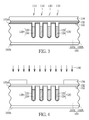
- the patterned hard mask 104 is removed and followed by sequentially forming a gate dielectric layer 122 and a gate conductive layer 124 in each trench 110 , and the trenches 110 are filled up with the gate conductive layer 124 . Consequently, a plurality of trenched gate 120 is formed in the trenches 110 , respectively. It is noteworthy that, according to the preferred embodiment, an etching back process is performed to the gate conductive layer 124 after forming the trenched gates 120 . Consequently, top surfaces of the trenched gates 120 , that are the top surfaces of the gate conductive layers 124 in the trenches 110 , are all lower than the openings of trenches 110 as shown in FIG. 2 .
- etching rate of the first insulating layer 132 is different from an etching rate of the pad layer 102
- the etching rate of the first insulating layer 132 is also different from an etching rate of the second insulating layer 134 .
- the pad layer 102 includes silicon oxide while the first insulating layer 132 includes silicon nitride, which includes etching rate different from silicon oxide.
- the second insulating layer 134 includes material having etching rate different from silicon nitride, such as silicon oxide, preferably tetraethylorthosilicate (TEOS), but not limited to this.
- silicon nitride such as silicon oxide, preferably tetraethylorthosilicate (TEOS), but not limited to this.
- TEOS tetraethylorthosilicate
- the first insulating layer 132 is blanketly formed to cover the entire front side 100 a of the substrate 100 . And thus the trenches 110 are filled up with the first insulating layer 132 .
- a thickness of the first insulating layer 132 can be 300 Angstrom ( ⁇ ) and a thickness of the second insulating layer 134 can be 3000 ⁇ , but not limited to this.
- a first etching process 140 is performed to remove portions of the second insulating layer 134 and to expose portions of the first insulating layer 132 .
- the first etching process 140 can be any proper etching process, for example but not limited to, the first etching process 140 can be a dry etching process. It is noteworthy that since the etching rate of the first insulating layer 132 is different from the etching rate of the second insulating layer 134 , the first insulating layer 132 serves as an etch stop layer in the first etching process 140 . In other words, the first insulating layer 132 protects the underneath gate dielectric layer 122 and pad layer 102 in the first etching process 140 .
- a second etching process 142 is performed to remove the exposed portions of the first insulating layer 132 and thus to expose portions of the trenched gates 120 .
- the second etching process 142 can be any proper etching process, for example but not limited to, the second etching process 142 can be a wet etching process.
- an isolation structure 130 is formed on the front side 100 a of the substrate 100 , particularly on the pad layer 102 , after the second etching process 142 according to the preferred embodiment.
- the isolation structure 130 includes at least the first insulating layer 132 and the second insulating layer 134 .
- the isolation structure 130 defines at least an active region 106 on the substrate 100 . As shown in FIG. 5 , the first insulating layer 132 of the isolation structure 130 is sandwiched between the second insulating layer 134 and the pad layer 102 .
- a bottom surface of the isolation structure 130 that is a bottom surface of the first insulating layer 132 , is higher than the top surfaces of the trenched gates 120 , that is the top surfaces of the gate conductive layers 124 .
- abase region 150 is formed in the substrate 100 , particularly formed in the n-typed epitaxial layer 100 E.
- the base region 150 includes a second conductivity type, and the second conductivity type is complementary with the first conductivity type. Therefore the base region 150 is a p-based region 150 according to the preferred embodiment.
- a semiconductor layer 160 is formed on the front side 100 a of the substrate 100 and on the second insulating layer 134 of the isolation structure 130 .
- the semiconductor layer 160 is then patterned to format least an electrode 162 .
- the electrode 162 strides over the isolation structure 130 and is electrically connected to one of the trenched gates 120 .
- FIG. 8 After forming the electrode 162 electrically connected to one of the trenched gates 120 , different ion implantations are performed to form a plurality of source regions 152 at two sides of each trenched gate 120 in the substrate 100 , and to forma doped region 154 in the base region 150 distal to the electrode 162 .
- the source regions 152 include the first conductivity type while the doped region 154 includes the second conductivity type. Therefore, the preferred embodiment provides n-source regions 152 and a p-doped region 154 .
- the heavily-doped n-region 100 N is taken as being formed on the back side 100 b of the substrate 100 . More important, the heavily-doped n-region 100 N serves as a drain region 156 .
- an insulating material layer 170 is formed on the substrate 100 .
- the insulating material layer 170 is blanketly formed on the front side 100 a of the substrate 100 , and the trenches 110 are filled up with the insulating material layer 170 .
- the insulating material layer 170 fills the trenches 110 , and thus covers and contacts the top surfaces of the trenched gates 120 .
- the insulating material layer 170 is patterned, and thus a plurality of openings 172 is formed in the insulating material layer 170 . As shown in FIG.
- the openings 172 expose at least a portion of the electrode 162 . More important, the openings 172 expose the source regions 152 and the doped region 154 on the front side 100 a of the substrate 100 . It should be noted that the top surfaces of the trenched gates 120 are still covered and protected by the insulating material layer 170 .
- post-salicide is optionally performed to form silicides (not shown) on silicon surface exposed at bottoms of each opening 172 for reducing contact resistance between the substrate 100 and following formed contacts. However, it should be easily realized by those skilled in the art that the silicide can be formed at different time points.
- a metal material is formed on the front side 100 a of the substrate 100 and followed by planarization. Consequently, a first metal layer 180 , a second metal layer 182 , and a third metal layer 184 are formed. As shown in FIG. 10 , the first metal layer 180 is electrically connected to the source regions 152 and the doped region 154 , the second metal layer 182 is electrically connected to the electrode 162 , and the third metal layer 184 is electrically connected to a patterned semiconductor layer 160 . Additionally, a fourth metal layer 186 is formed on the back side 100 b of the substrate 100 . And thus a vertical double-diffused MOS (VDMOS) is constructed and obtained according to the preferred embodiment.
- VDMOS vertical double-diffused MOS
- the isolation structure used to define the active region(s) and provide electrical isolation is formed by depositions after forming the trenched gates. Since the isolation structure is no longer formed by LOCOS method, high-temperature process is not required. Therefore the isolation structure can be formed at other time point, instead of the beginning the whole manufacturing process. And thus process flexibility is improved. More important, because the isolation structure is formed on the substrate by depositions, silicon consumption and birds' beak effect to the substrate are all avoided.
Landscapes
- Engineering & Computer Science (AREA)
- Power Engineering (AREA)
- Microelectronics & Electronic Packaging (AREA)
- Condensed Matter Physics & Semiconductors (AREA)
- General Physics & Mathematics (AREA)
- Physics & Mathematics (AREA)
- Computer Hardware Design (AREA)
- Ceramic Engineering (AREA)
- Manufacturing & Machinery (AREA)
- Element Separation (AREA)
- Chemical & Material Sciences (AREA)
- Chemical Kinetics & Catalysis (AREA)
- General Chemical & Material Sciences (AREA)
- Inorganic Chemistry (AREA)
- Insulated Gate Type Field-Effect Transistor (AREA)
Abstract
Description
Claims (13)
Priority Applications (1)
| Application Number | Priority Date | Filing Date | Title |
|---|---|---|---|
| US15/151,506 US9502508B2 (en) | 2014-11-11 | 2016-05-11 | Method for manufacturing isolation structure integrated with semiconductor device |
Applications Claiming Priority (5)
| Application Number | Priority Date | Filing Date | Title |
|---|---|---|---|
| TW103139109 | 2014-11-11 | ||
| TW103139109A | 2014-11-11 | ||
| TW103139109A TWI636504B (en) | 2014-11-11 | 2014-11-11 | Isolation structure integrated with semiconductor device and manufacturing method thereof |
| US14/569,772 US9859377B2 (en) | 2014-11-11 | 2014-12-14 | Isolation structure integrated with semiconductor device and manufacturing method thereof |
| US15/151,506 US9502508B2 (en) | 2014-11-11 | 2016-05-11 | Method for manufacturing isolation structure integrated with semiconductor device |
Related Parent Applications (1)
| Application Number | Title | Priority Date | Filing Date |
|---|---|---|---|
| US14/569,772 Division US9859377B2 (en) | 2014-11-11 | 2014-12-14 | Isolation structure integrated with semiconductor device and manufacturing method thereof |
Publications (2)
| Publication Number | Publication Date |
|---|---|
| US20160254354A1 US20160254354A1 (en) | 2016-09-01 |
| US9502508B2 true US9502508B2 (en) | 2016-11-22 |
Family
ID=55912808
Family Applications (2)
| Application Number | Title | Priority Date | Filing Date |
|---|---|---|---|
| US14/569,772 Active 2035-05-07 US9859377B2 (en) | 2014-11-11 | 2014-12-14 | Isolation structure integrated with semiconductor device and manufacturing method thereof |
| US15/151,506 Active US9502508B2 (en) | 2014-11-11 | 2016-05-11 | Method for manufacturing isolation structure integrated with semiconductor device |
Family Applications Before (1)
| Application Number | Title | Priority Date | Filing Date |
|---|---|---|---|
| US14/569,772 Active 2035-05-07 US9859377B2 (en) | 2014-11-11 | 2014-12-14 | Isolation structure integrated with semiconductor device and manufacturing method thereof |
Country Status (2)
| Country | Link |
|---|---|
| US (2) | US9859377B2 (en) |
| TW (1) | TWI636504B (en) |
Families Citing this family (1)
| Publication number | Priority date | Publication date | Assignee | Title |
|---|---|---|---|---|
| CN114078748B (en) * | 2020-08-14 | 2024-08-09 | 长鑫存储技术有限公司 | Semiconductor device and method for manufacturing the same |
Citations (5)
| Publication number | Priority date | Publication date | Assignee | Title |
|---|---|---|---|---|
| US6921932B1 (en) | 2002-05-20 | 2005-07-26 | Lovoltech, Inc. | JFET and MESFET structures for low voltage, high current and high frequency applications |
| US7193262B2 (en) | 2004-12-15 | 2007-03-20 | International Business Machines Corporation | Low-cost deep trench decoupling capacitor device and process of manufacture |
| US8232187B2 (en) | 2009-07-31 | 2012-07-31 | Hynix Semiconcuctor Inc. | Doping method for semiconductor device |
| US8809993B2 (en) | 2012-03-19 | 2014-08-19 | Samsung Electronics Co., Ltd. | Semiconductor device having isolation region |
| US9318566B2 (en) * | 2013-03-27 | 2016-04-19 | Samsung Electronics Co., Ltd. | Method of fabricating semiconductor device having grooved source contact region |
-
2014
- 2014-11-11 TW TW103139109A patent/TWI636504B/en active
- 2014-12-14 US US14/569,772 patent/US9859377B2/en active Active
-
2016
- 2016-05-11 US US15/151,506 patent/US9502508B2/en active Active
Patent Citations (5)
| Publication number | Priority date | Publication date | Assignee | Title |
|---|---|---|---|---|
| US6921932B1 (en) | 2002-05-20 | 2005-07-26 | Lovoltech, Inc. | JFET and MESFET structures for low voltage, high current and high frequency applications |
| US7193262B2 (en) | 2004-12-15 | 2007-03-20 | International Business Machines Corporation | Low-cost deep trench decoupling capacitor device and process of manufacture |
| US8232187B2 (en) | 2009-07-31 | 2012-07-31 | Hynix Semiconcuctor Inc. | Doping method for semiconductor device |
| US8809993B2 (en) | 2012-03-19 | 2014-08-19 | Samsung Electronics Co., Ltd. | Semiconductor device having isolation region |
| US9318566B2 (en) * | 2013-03-27 | 2016-04-19 | Samsung Electronics Co., Ltd. | Method of fabricating semiconductor device having grooved source contact region |
Also Published As
| Publication number | Publication date |
|---|---|
| US20160133479A1 (en) | 2016-05-12 |
| US20160254354A1 (en) | 2016-09-01 |
| TWI636504B (en) | 2018-09-21 |
| US9859377B2 (en) | 2018-01-02 |
| TW201618185A (en) | 2016-05-16 |
Similar Documents
| Publication | Publication Date | Title |
|---|---|---|
| US9660022B2 (en) | Semiconductive device with a single diffusion break and method of fabricating the same | |
| TWI525821B (en) | Mosfet device and method for manufacturing the same | |
| JP5752810B2 (en) | Semiconductor device | |
| US8987820B1 (en) | Lateral double diffused metal-oxide-semiconductor device and method for fabricating the same | |
| US20070145491A1 (en) | Semiconductor device and method of manufacture | |
| US9461036B2 (en) | Semiconductor device | |
| US11075292B2 (en) | Insulated gate bipolar transistor, and manufacturing method therefor | |
| JP5692886B1 (en) | Semiconductor device manufacturing method and semiconductor device | |
| US9502508B2 (en) | Method for manufacturing isolation structure integrated with semiconductor device | |
| JP6115243B2 (en) | Semiconductor device and manufacturing method of semiconductor device | |
| JP2005039057A (en) | Semiconductor device and its manufacturing method | |
| US7714382B2 (en) | Trench gate semiconductor with NPN junctions beneath shallow trench isolation structures | |
| US8822296B2 (en) | Use of plate oxide layers to increase bulk oxide thickness in semiconductor devices | |
| JP2013045953A (en) | Semiconductor device and method of manufacturing the same | |
| CN108305830A (en) | Semiconductor structure and forming method thereof | |
| US20090134477A1 (en) | Semiconductor device and method of fabricating the same | |
| US10290728B2 (en) | Semiconductor device and manufacturing method thereof | |
| TW202021082A (en) | Semiconductor device and method for manufacturing the same | |
| JP5928566B2 (en) | Semiconductor device manufacturing method and semiconductor device | |
| JP5685344B2 (en) | Semiconductor device manufacturing method and semiconductor device | |
| US9634099B2 (en) | Lateral double diffused metal-oxide-semiconductor device and method for fabricating the same | |
| US7812415B2 (en) | Apparatus having gate structure and source/drain over semiconductor substrate | |
| KR100730476B1 (en) | Manufacturing method of semiconductor device | |
| JPWO2014115287A1 (en) | Semiconductor device manufacturing method and semiconductor device | |
| KR20100074422A (en) | Semiconductor device and method for manufacturing the device |
Legal Events
| Date | Code | Title | Description |
|---|---|---|---|
| AS | Assignment |
Owner name: UNITED MICROELECTRONICS CORP., TAIWAN Free format text: ASSIGNMENT OF ASSIGNORS INTEREST;ASSIGNORS:LIN, HONG-ZE;HUANG, CHIEN-MING;LIN, SHIN-KUANG;REEL/FRAME:038542/0096 Effective date: 20141107 |
|
| STCF | Information on status: patent grant |
Free format text: PATENTED CASE |
|
| MAFP | Maintenance fee payment |
Free format text: PAYMENT OF MAINTENANCE FEE, 4TH YEAR, LARGE ENTITY (ORIGINAL EVENT CODE: M1551); ENTITY STATUS OF PATENT OWNER: LARGE ENTITY Year of fee payment: 4 |
|
| MAFP | Maintenance fee payment |
Free format text: PAYMENT OF MAINTENANCE FEE, 8TH YEAR, LARGE ENTITY (ORIGINAL EVENT CODE: M1552); ENTITY STATUS OF PATENT OWNER: LARGE ENTITY Year of fee payment: 8 |