US9501282B2 - Arithmetic processing device - Google Patents
Arithmetic processing device Download PDFInfo
- Publication number
- US9501282B2 US9501282B2 US14/186,095 US201414186095A US9501282B2 US 9501282 B2 US9501282 B2 US 9501282B2 US 201414186095 A US201414186095 A US 201414186095A US 9501282 B2 US9501282 B2 US 9501282B2
- Authority
- US
- United States
- Prior art keywords
- instruction
- unit
- stream
- arithmetic
- memory
- Prior art date
- Legal status (The legal status is an assumption and is not a legal conclusion. Google has not performed a legal analysis and makes no representation as to the accuracy of the status listed.)
- Expired - Fee Related, expires
Links
Images


Classifications
-
- G—PHYSICS
- G06—COMPUTING OR CALCULATING; COUNTING
- G06F—ELECTRIC DIGITAL DATA PROCESSING
- G06F9/00—Arrangements for program control, e.g. control units
- G06F9/06—Arrangements for program control, e.g. control units using stored programs, i.e. using an internal store of processing equipment to receive or retain programs
- G06F9/30—Arrangements for executing machine instructions, e.g. instruction decode
- G06F9/38—Concurrent instruction execution, e.g. pipeline or look ahead
- G06F9/3824—Operand accessing
- G06F9/383—Operand prefetching
-
- G—PHYSICS
- G06—COMPUTING OR CALCULATING; COUNTING
- G06F—ELECTRIC DIGITAL DATA PROCESSING
- G06F9/00—Arrangements for program control, e.g. control units
- G06F9/06—Arrangements for program control, e.g. control units using stored programs, i.e. using an internal store of processing equipment to receive or retain programs
- G06F9/30—Arrangements for executing machine instructions, e.g. instruction decode
- G06F9/38—Concurrent instruction execution, e.g. pipeline or look ahead
- G06F9/3824—Operand accessing
-
- G—PHYSICS
- G06—COMPUTING OR CALCULATING; COUNTING
- G06F—ELECTRIC DIGITAL DATA PROCESSING
- G06F9/00—Arrangements for program control, e.g. control units
- G06F9/06—Arrangements for program control, e.g. control units using stored programs, i.e. using an internal store of processing equipment to receive or retain programs
- G06F9/30—Arrangements for executing machine instructions, e.g. instruction decode
- G06F9/38—Concurrent instruction execution, e.g. pipeline or look ahead
- G06F9/3877—Concurrent instruction execution, e.g. pipeline or look ahead using a slave processor, e.g. coprocessor
Definitions
- the embodiment discussed herein is related to an arithmetic processing device.
- LTE Long Term Evolution
- LTE Advanced which is a higher-performance next-generation mobile communications system
- LTE Advanced when LTE Advanced is employed, an enormous amount of matrix arithmetic operation processing is to be performed as wireless-communication baseband processing. This is not only limited to LTE Advanced, but is also true for various wireless communication systems (standards) including Worldwide Interoperability for Microwave Access 2 (WiMAX 2) and currently used systems.
- WiMAX 2 Worldwide Interoperability for Microwave Access 2
- a configuration in which a memory in which matrix data is stored and an arithmetic unit are connected in series and a stream engine performs matrix arithmetic operation on data read from the memory and writes out an arithmetic-operation result to the memory is suitable, in order to execute matrix arithmetic operation processing (one type of stream processing) at high speed.
- a base processor which is a general-purpose processor
- a coprocessor having a stream engine has been proposed as an arithmetic processing device (an arithmetic processing system) for performing wireless-communication baseband processing in LTE Advanced.
- Examples of related art include the technologies disclosed in Japanese Laid-open Patent Publication No. 2011-197774 and Japanese Laid-open Patent Publication No. 08-069377.
- interrupt processing is performed after waiting until the execution of the stream processing is completed.
- the base processor waits until the coprocessor enters an idle state. This further increases the communication cycle overhead.
- An object of the embodiments is providing a combination of a base processor and a coprocessor having a stream engine for an arithmetic processing system for performing wireless-communication baseband processing.
- an arithmetic processing device includes: an arithmetic unit configured to execute an arithmetic operation; and a stream engine configured to execute stream processing, wherein a data bus of the arithmetic unit and a data bus of the stream engine are tightly coupled with each other.
- FIG. 1 is a block diagram illustrating an example of an arithmetic processing device
- FIG. 2 is a block diagram illustrating an example of the arithmetic processing device according to the present embodiment
- FIG. 3 is a block diagram illustrating an operation performed by the arithmetic processing device according to the present embodiment
- FIG. 4 is a block diagram illustrating an operation of stopping a stream engine in the arithmetic processing device according to the present embodiment
- FIGS. 5A and 5B are diagrams illustrating an example of an advantage resulting from the stopping operation of the stream engine, the stopping operation being described with reference to FIG. 4 ;
- FIG. 6 is a diagram illustrating an example of an operation of a reading circuit in the arithmetic processing device according to the present embodiment
- FIG. 7 is a diagram illustrating another example of the reading circuit in the arithmetic processing device according to the present embodiment.
- FIG. 8 is a diagram illustrating an example of an operation of an executing circuit in the arithmetic processing device according to the present embodiment
- FIG. 9 is a diagram illustrating another example of the operation of the executing circuit in the arithmetic processing device according to the present embodiment.
- FIG. 10 is a diagram illustrating an example of the operation of a writing circuit in the arithmetic processing device according to the present embodiment
- FIG. 11 is a diagram illustrating another example of the operation of the writing circuit in the arithmetic processing device according to the present embodiment.
- FIG. 12 is a diagram illustrating an example of parameter information in the arithmetic processing device according to the present embodiment.
- FIG. 13 is a diagram (part 1 ) illustrating step instructions in the arithmetic processing device according to the present embodiment
- FIGS. 14A to 14C are a diagrams (part 2 ) illustrating step instructions in the arithmetic processing device according to the present embodiment
- FIG. 15 is a diagram illustrating a modification of the step instructions in the arithmetic processing device according to the present embodiment
- FIG. 16 is a diagram (part 1 ) illustrating micro instructions in the arithmetic processing device according to the present embodiment
- FIG. 17A to 17C are diagrams (part 2 ) illustrating micro instructions in the arithmetic processing device according to the present embodiment
- FIGS. 18A to 18C are diagrams illustrating access control according to micro instructions in the arithmetic processing device according to the present embodiment
- FIG. 19 illustrates a state in which micro instructions in the arithmetic processing device according to the present embodiment are embedded in VLIW instructions
- FIGS. 20A to 20C are diagrams illustrating prologue processing according to the VLIW instructions illustrated in FIG. 19 ;
- FIGS. 21A to 21C are diagrams illustrating epilogue processing according to the VLIW instructions illustrated in FIG. 19 .
- FIG. 1 is a block diagram illustrating an example of an arithmetic processing device.
- the illustrated arithmetic processing device (arithmetic processing system) is a combination of a base processor, which is a general-purpose processor, and a coprocessor having a stream engine.
- reference character IF indicates an instruction fetching (Instruction Fetch) stage
- ID indicates an instruction decoding (Instruction Decode) stage
- RR/II indicates a register reading (Register Read) stage and an instruction issuing (Instruction Issue) stage.
- Reference character EX indicates an execution (EXecution) stage
- MA indicates a memory access (Memory Access) stage
- RW indicates a register writing (Register Write) stage.
- the arithmetic processing system illustrated in FIG. 1 has, for example, a base processor 100 , which is a general-purpose processor, and a coprocessor 300 , which includes a stream engine 200 .
- an instruction fetching unit 101 fetches (reads) an instruction from an instruction memory 108
- an instruction decoding unit 102 receives the instruction read by the instruction fetching unit 101 and decodes (interprets) the instruction.
- a register reading unit 103 performs reading from a register 110 , and an instruction issuing unit 104 issues the instruction interpreted by the instruction decoding unit 102 to an arithmetic unit 105 .
- the arithmetic unit 105 executes an arithmetic operation according to the instruction issued by the instruction issuing unit 104 , and in the MA stage, a memory access unit 106 makes access, involving load (read) or store (write), to a memory (data memory) 109 .
- a register writing unit 107 writes, to the register 110 , an arithmetic-operation result obtained by the arithmetic unit 105 or data loaded from the data memory 109 .
- the base processor 100 is adapted to perform pipeline execution, regarding processing between the register 110 and the memory 109 or between the register 110 and the arithmetic unit 105 as processing according to a single instruction.
- an instruction fetching unit 301 reads an instruction from the instruction memory 108
- an instruction decoding unit 302 reads and interprets the instruction read by the instruction fetching unit 301 .
- a register reading unit 303 performs reading from a register 310
- an instruction issuing unit 304 issues the instruction interpreted by the instruction decoding unit 302 to the stream engine 200 .
- the stream engine 200 includes an arithmetic unit 205 and a memory access unit 206 , which makes access, involving load or store, to a data memory 400 .
- the instruction from the instruction issuing unit 304 to the stream engine 200 is a stream instruction.
- pipeline execution is performed until one sequence of stream processing between the memory 400 and the arithmetic unit 205 is completed.
- the arithmetic unit 205 and the memory access unit 206 in the stream engine 200 perform processing until the stream processing is completed, in accordance with a stream instruction issued from the instruction issuing unit 304 .
- a register writing unit 307 writes data (an arithmetic-operation result), subjected to the stream processing by the stream engine 200 , to the register 310 .
- reference character P 150 indicates processing that the base processor 100 performs on the coprocessor 300 , for example, processing for handshaking with the coprocessor 300 by issuing a stream instruction to the coprocessor 300 . That is, the base processor 100 monitors, for example, the state of the coprocessor 300 , controls execution of the coprocessor 300 , and controls data transfer to the coprocessor 300 .
- the arithmetic processing system which is a combination of the base processor 100 and the coprocessor 300 having the stream engine 200 , described above with reference to FIG. 1 has a problem of cycle overhead when the stream engine 200 executes stream processing.
- the base processor 100 monitors the state of the coprocessor 300 through handshaking to perform data transfer with the coprocessor 300 and controls execution of the coprocessor 300 .
- overhead occurs between the base processor 100 and the coprocessor 300 .
- the stream engine 200 waits until the execution of the stream processing is completed, and thus the communication cycle overhead further increases.
- FIG. 2 is a block diagram illustrating an example of the arithmetic processing device according to the present embodiment.
- an arithmetic processing device (processor) 1 illustrated in FIG. 2 includes a configuration corresponding to the base processor 100 illustrated in FIG. 1 and further includes a stream engine 2 .
- the processor 1 includes a register 10 , an instruction fetching unit 11 , an instruction decoding unit 12 , a register reading unit 13 , an instruction issuing unit 14 , an arithmetic unit 15 , a memory access unit 16 , a register writing unit 17 , an instruction memory 18 , and a data memory 19 .
- the instruction issuing unit 14 is adapted to not only issue instructions to the arithmetic unit 15 , but also issue instructions (for example, step instructions) to the stream engine 2 .
- the stream engine 2 includes a pop unit 21 and an exec unit 23 .
- the pop unit 21 reads data from a data memory 4 and writes the read data to registers 221 and 222
- the exec unit 23 executes stream processing on the data written to the registers 221 and 222 and writes the resulting data to a register 24 .
- the stream engine 2 further includes a push unit 25 that writes the data, written to the register 24 , to the data memory 4 .
- reference characters IF, ID, RR/II, EX, MA, and RW indicate stages that are the same as or similar to those described above with reference to FIG. 1 .
- the instruction fetching unit 11 fetches (reads) an instruction from the instruction memory 18
- the instruction decoding unit 102 receives the instruction fetched by the instruction fetching unit 101 and decodes (interprets) the instruction.
- the register reading unit 13 performs reading from the register 10 , and the instruction issuing unit 14 issues the instruction, interpreted by the instruction decoding unit 12 , to the arithmetic unit 15 and the stream engine 2 .
- the arithmetic unit 15 executes an arithmetic operation according to the instruction issued from the instruction issuing unit 14
- the stream engine 2 executes stream processing according to the instruction issued from the instruction issuing unit 14 .
- the instructions issued from the instruction issuing unit 14 to the stream engine 2 are step instructions, as described above.
- the memory access unit 16 makes access, involving load or store, to the memory (data memory) 19 .
- the stream engine 2 (the pop unit 21 or the push unit 25 ) makes access, involving load (read) or store (write), to the memory (data memory) 4 .
- the register writing unit 17 writes an arithmetic-operation result, obtained by the arithmetic unit 15 , or data, loaded from the data memory 19 , to the register 10 , and the register writing unit 17 writes the data, subjected to the stream processing executed by the stream engine 2 , to the register 10 .
- FIG. 3 is a block diagram illustrating an operation performed by the arithmetic processing device 1 according to the present embodiment. As is apparent from comparison between reference character P 1 illustrated in FIG. 3 and reference character P 100 illustrated in FIG. 1 , pipeline execution is performed regarding processing between the register 10 and the memory 19 or the register 10 and the arithmetic unit 15 as processing according to a single instruction in a portion corresponding to the base processor 100 illustrated in FIG. 1 .
- the stream engine 2 which is built into the processor 1 , executes processes for the respective steps in accordance with step instructions issued from the instruction issuing unit 14 .
- the process P 21 is a process in which the pop unit 21 in the stream engine 2 reads data from the data memory 4 and writes the read data to the registers 221 and 222 .
- the process P 22 is a process in which the exec unit 23 executes stream processing on the data written to the registers 221 and 222 and writes the resulting data to the register 24 .
- process P 23 is a process in which the push unit 25 writes the data, written to the register 24 , to the data memory 4 .
- the processes P 21 to P 23 are subjected to pipeline execution according to step instructions issued from the instruction issuing unit 14 .
- FIG. 4 is a block diagram illustrating an operation of stopping the stream engine 2 in the arithmetic processing device 1 according to the present embodiment. For example, when an interrupt occurs while the stream engine 2 , built into the processor 1 , is executing stream processing, the instruction issuing unit 14 stops the issuance of the step instructions to the stream engine 2 .
- the exec unit 23 also stops the process P 22 in which the stream processing is executed on the data written to the registers 221 and 222 and the resulting data is written to the register 24 .
- the push unit 25 then stops the process P 23 in which the data written to the register 24 is written to the data memory 19 .
- the arithmetic processing device performs fine-grained control on the operation of the stream engine 2 in accordance with the step instructions.
- the arithmetic processing device can perform interrupt processing by immediately stopping the stream processing.
- the arithmetic processing device for example, it is possible to immediately stop the stream engine 2 by stopping the issuance of the step instructions during occurrence of an interrupt.
- the pipeline stages (processes P 21 to P 23 ) in the stream engine 2 can autonomously be stopped, thus making it possible to reduce the cycle overhead and to increase the processing speed.
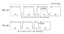
- FIGS. 5A and 5B are diagrams illustrating an example of an advantage resulting from the stopping operation of the stream engine 2 , the stopping operation being described above with reference to FIG. 4 . More specifically, FIG. 5A illustrates an operation performed by the arithmetic processing system described above illustrated in FIG. 1 , and FIG. 5B illustrates an operation performed by the arithmetic processing device described above with reference to FIG. 4 .
- the number of cycles (the number of clock cycles) of one sequence of stream processing is 200 cycles
- latency of an arithmetic-operation data bus is 10 cycles
- the bit width of parameter information used for one sequence of stream processing is 320 bits.
- a data bus between the base processor 100 and the coprocessor 300 is a 32-bit data bus and the parameter information is transferred from the base processor 100 to the coprocessor 300 at 10 cycles.
- the parameter information is assumed to be transferred at 1 cycle.
- the term “tight coupling” as used herein does not mean that processors coupled at a bus level access a common memory, and means that the common instruction issuing unit 14 issues an instruction to the arithmetic unit 15 and the stream engine 2 .
- the arithmetic processing device (processor) 1 in the embodiment described above with reference to FIG. 4 for example, when an interrupt occurs at the 50th cycle in the third stream processing (A 2 ), the third stream processing is immediately stopped and the stream processing (B 0 ) is executed.
- the processor 1 in the present embodiment allows the processing speed to be increased from 860 cycles to 683 cycles by 177 cycles.
- FIGS. 5A and 5B illustrate merely an example of stream processing, and it goes without saying that, for example, the larger the number of cycles according to one stream instruction is or the higher the frequency of occurrence of an interrupt during execution of stream processing is, the greater the advantage of increasing the processing speed becomes.
- FIG. 6 is a diagram illustrating an example of an operation of a reading circuit in the arithmetic processing device according to the present embodiment
- FIG. 7 is a diagram illustrating another example of the reading circuit in the arithmetic processing device according to the present embodiment.
- a reading circuit 210 includes a pop unit 21 and registers 221 and 222 , and a data memory 4 includes memory portions 41 and 42 .
- the memory portions 41 and 42 represent, for example, banked memory areas at different addresses (start addresses) in the data memory 4 and may, needless to say, include any number of memories other than two memories.
- the pop unit 21 in the reading circuit 210 reads first data from the memory portion (a first bank) 41 in the data memory 4 by specifying the start address and a stream length and stores the read first data in the register 221 .
- the pop unit 21 in the reading circuit 210 reads second data from the memory portion (a second bank) 42 in the data memory 4 by specifying the start address and a stream length and stores the read second data in the register 222 .
- the processing of the reading circuit 210 corresponds to, for example, the above-described process P 21 in the arithmetic processing device described above and illustrated in FIG. 3 .
- the pop unit 21 reads stream data from the data memory 4 , inputs (stores) the stream data to (in) the registers (pipeline registers) 221 and 222 between a reading stage (the pop unit 21 ) and an execution stage (the exec unit 23 ) for the stream processing, and executes pipeline processing.
- specifying the start address and the stream length to read stream data from the data memory 4 , banked into the first bank 41 and the second bank 42 makes it possible to reduce the number of memory ports and to minimize the cycle overhead.
- data read from the memory portions (the first and second banks) 41 and 42 by direct memory access (DMA) unit 5 may also be supplied to the reading circuit 210 through first-in first-out (FIFO) buffers 61 and 62 . That is, transferring of data from the data memory 4 may also be left to the DMA unit 5 to extract read data from the FIFO buffers 61 and 62 .
- DMA direct memory access
- FIG. 8 is a diagram illustrating an example of an operation of an executing circuit in the arithmetic processing device 1 according to the present embodiment.
- an executing circuit 230 includes an exec unit 23 and a register 24 .
- the exec unit 23 in the executing circuit 230 executes stream processing on data written to the registers 221 and 222 and writes an arithmetic-operation result thereof to the register 24 .
- the processing of the executing circuit 230 corresponds to, for example, the process P 22 in the arithmetic processing device 1 described above and illustrated in FIG. 3 .
- the exec unit 23 executes stream processing on data input to the registers 221 and 222 , inputs an arithmetic-operation result thereof to the register (pipeline register) 24 between the exec unit 23 and the push unit 25 and executes pipeline processing.
- FIG. 9 is a diagram illustrating another example of the operation of the executing circuit in the arithmetic processing device 1 according to the present embodiment.
- this executing circuit 230 is constituted by exec units 231 to 233 and registers 241 to 243 in multiple stages.
- four registers 221 a and 221 b and 222 a and 222 b are provided in the reading circuit 210 so as to correspond to two exec units 231 and 232 .
- Three registers 241 to 243 are also provided in the executing circuit 230 in order to store arithmetic-operation results obtained by the three exec units 231 to 233 .
- the executing circuit 230 illustrated in FIG. 9 is merely an example, and it goes without saying that various other configurations may also be used.
- the executing circuit 230 (the data bus of the arithmetic unit) may have a multi-stage configuration. With this configuration, an arithmetic-operation result may be input to the register (pipeline register) 243 between the exec unit 233 and a push unit 25 to execute pipeline processing.
- FIG. 10 is a diagram illustrating an example of the operation of a writing circuit in the arithmetic processing device 1 according to the present embodiment
- FIG. 11 is a diagram illustrating another example of the operation of the writing circuit in the arithmetic processing device 1 according to the present embodiment.
- a writing circuit 250 includes a push unit 25 and writes the arithmetic-operation result stored in a register 24 to a memory portion 43 in a data memory 4 . That is, the writing circuit 250 extracts output data from the pipeline register 24 between the exec unit 23 and the push unit 25 and writes the output data to, for example, a memory area indicated by a start address and a stream length.
- the processing of the writing circuit 250 corresponds to, for example, the process P 23 in the arithmetic processing device 1 described above and illustrated in FIG. 3 .
- the memory unit 43 may be, for example, a memory area that is different from the memory portions 41 and 42 in the data memory 4 .
- the writing circuit 250 illustrated in FIG. 10 directly writes the arithmetic-operation result, stored in the register 24 , to the memory portion 43 .
- a writing circuit 250 illustrated in FIG. 11 writes an arithmetic-operation result, stored in a register 24 , to a FIFO buffer 7 , and a DMA unit 8 transfers the data, written to the FIFO buffer 7 , to a memory portion 43 .
- the writing circuit 250 illustrated in FIG. 11 is adapted to sequentially write the arithmetic-operation results, stored in the register 24 , to the FIFO buffer 7 and to leave the data transfer from the FIFO buffer 7 to the memory portion 43 (a data memory 4 ) to the DMA unit 8 .
- FIG. 12 is a diagram illustrating an example of the parameter information in the arithmetic processing device 1 according to the present embodiment.
- the parameter information used in the stream processing may be represented by, for example, the start address (ai) of each stream (i), a stream length (li), an arithmetic-operation opcode (o), and an arithmetic-operation mode (m), and a single large-bit-length set instruction (a set instruction: set).
- the set instruction (the parameter information) is read from the instruction memory 18 and is assigned to (set in) a parameter register 140 at once, as indicated by reference character P 10 .
- the pipeline stages (the pop unit 21 , the exec unit 23 , and the push unit 25 ) refer to the parameter information in the parameter register 140 to perform pipeline execution, as indicated by reference character P 11 .
- FIGS. 13 to 14C are diagrams illustrating step instructions in the arithmetic processing device 1 according to the present embodiment. As illustrated in FIGS. 13 to 14C , according to the arithmetic processing device (the stream engine 2 ) in the present embodiment, it is possible to perform control in accordance with the set instruction.
- step instructions are read from the instruction memory 18 , as indicated by reference character P 20 , and are executed to thereby make it possible to control the processes P 21 to P 23 in the respective pipeline stages in the stream engine 2 .
- the step instructions are, for example, instructions created by a programmer in advance.
- step instructions “steps 1 to N” are read from the instruction memory 18 in order and are issued from the instruction issuing unit 14 to the stream engine 2 , and the pipeline processes P 21 to P 23 are executed.
- the step instructions are issued from the instruction issuing unit 14 to the stream engine 2 , and the pop unit 21 , the exec unit 23 , and the push unit 25 execute corresponding processes (P 21 , P 22 , and P 23 ) in accordance with the respective step instructions.
- the process P 21 is a process in which the pop unit 21 reads data from the data memory 4 and writes the data to the registers 221 and 222 .
- the process P 22 is a process in which the exec unit 23 executes stream processing on the data written to the registers 221 and 222 and writes the resulting data to the register 24 .
- the process P 23 is a process in which the push unit 25 writes the data, written to the register 24 , to the data memory 19 .
- These processes P 21 to P 23 are subjected to pipeline execution in accordance with the step instructions issued from the instruction issuing unit 14 .
- FIG. 15 is a diagram illustrating a modification of the step instructions in the arithmetic processing device 1 according to the present embodiment.
- N step instructions “steps 1 to N” are read directly from the instruction memory 18 and are issued from the instruction issuing unit 14 to the stream engine 2 .
- set instructions are combined with an instruction (a zero-overhead loop instruction) dedicated to loop processing for efficiently executing a continuously repeated process (loop processing).
- combining N step instructions “steps 1 to N” with a zero-overhead loop instruction makes it possible to suppress an increase in the number of instruction sequences.
- the zero-overhead loop instruction for example, when an interrupt occurs, the processing of a stream is immediately stopped in a step being executed.
- FIGS. 16 to 17C are diagrams illustrating micro instructions in the arithmetic processing device according to the present embodiment. As illustrated in FIG. 16 , instructions issued from the instruction issuing unit 14 to the stream engine 2 are micro instructions.
- the arithmetic processing device is adapted such that micro instructions are read from the instruction memory 18 and are executed to control processes P 21 to P 23 in the respective pipeline stages in the stream engine 2 .
- a pop instruction is assigned to the process P 21 illustrated in FIG. 17A
- an exec instruction is assigned to the process P 22 illustrated in FIG. 17B
- a push instruction is assigned to the process P 23 illustrated in FIG. 17C
- the processes P 21 to P 23 are executed according to the micro instructions. This arrangement allows the processes P 21 to P 23 in the respective pipeline stages to be individually controlled according to the micro instructions.
- FIGS. 18A to 18C are diagrams illustrating access control according to micro instructions in the arithmetic processing device according to the present embodiment.
- FIG. 18A illustrates a case in which all of a pop instruction, an exec instruction, and a push instruction are issued
- FIG. 18B illustrates a case in which a pop instruction is stopped
- FIG. 18C illustrates a case in which a push instruction is stopped.
- the arithmetic processing device includes DMA units 5 and 8 and FIFO buffers 61 , 62 , and 7 , similarly to the configurations illustrated in FIGS. 7 and 11 .
- the pop unit 21 stops the reading of data from the FIFO buffers 61 and 62 .
- the DMA unit (input DMA unit) 5 As a result of data transfer performed by the DMA unit (input DMA unit) 5 , the FIFO buffers 61 and 62 are filled up, and the DMA unit 5 detects the fill-up states of the FIFO buffers 61 and 62 and makes an automatic stop. That is, by stopping the pop instruction, which is a micro instruction, it is possible to stop the pipeline processing of the stream engine 2 .
- the push unit 25 stops the operation for reading data from the register 24 and storing the data in the FIFO buffer 7 .
- the FIFO buffer 7 becomes empty and the DMA (output DMA) unit 8 detects the empty state of the FIFO buffer 7 and makes an automatic stop. That is, by stopping the push instruction, which is a micro instruction, it is possible to stop the pipeline processing of the stream engine 2 .
- micro instructions namely, the pop instruction, the exec instruction, and the push instruction
- the DMA units 5 and 8 allows the DMA units 5 and 8 to autonomously control memory access, for example, even when an interrupt occurs. That is, it is possible to simplify control of data transfer between the memory 19 and the arithmetic unit 15 , thus making it possible to reduce the amount of hardware for memory access control.
- FIG. 19 illustrates a state in which micro instructions in the arithmetic processing device according to the present embodiment are embedded in (packed into) VLIW instructions.
- VLIW very long instruction word
- embedding a plurality of micro instructions in VLIW instructions makes it possible to reduce the number of instructions in the loop processing and further makes it possible to reduce the number of execution cycles in the loop. Such an arrangement also makes it possible to effectively use the instruction set architecture of the base processor (which may be a VLIW processor, in the arithmetic processing device 1 ).
- FIG. 19 illustrates a state in which M micro instructions are packed into N VLIW instructions.
- prologue processing according to a VLIW 1 instruction to a VLIW 3 instruction and epilogue processing according to a VLIW N- 2 instruction to a VLIW N instruction will be described with reference to FIGS. 20A to 21C .
- FIGS. 20A to 20C are diagrams illustrating prologue processing according to the VLIW instructions illustrated in FIG. 19 . More specifically, FIG. 20A illustrates processing according to the VLIW 1 instruction, FIG. 20B illustrates processing according to the VLIW 2 instruction, and FIG. 20C illustrates processing according to the VLIW 3 instruction.
- the prologue processing is processing for activating the stream engine 2 and is realized by executing three instructions, namely, VLIW 1 [pop], VLIW 2 [pop, exec], and VLIW 3 [pop, exec, push].
- a pop instruction which is a VLIW 1 instruction
- the process P 21 in which the pop unit 21 reads data from the data memory 4 and writes the data to the registers 221 and 222 is executed according to the pop instruction.
- the data on which the exec unit 23 is to perform arithmetic operation processing is input to the registers 221 and 222 .
- the pop instruction and the exec instruction which are included in the VLIW 2 instruction, are executed. That is, the process P 21 is executed according to the pop instruction, and also the process P 22 in which the exec unit 23 executes stream processing on the data written to the registers 221 and 222 and writes the resulting data to the register 24 is executed according to the exec instruction.
- the data that the exec unit 23 is to perform arithmetic operation processing is input to the registers 221 and 222 and the arithmetic-operation-result data the push unit 25 is to write to the data memory 4 is input to the register 24 .
- the pop instruction, the exec instruction, and the push instruction which are included in the VLIW 3 instruction, are executed.
- the process P 21 is executed according to the pop instruction
- the process P 22 is executed according to the exec instruction
- the process P 23 in which the push unit 25 writes the arithmetic-operation-result data, written to the register 24 , to the data memory 4 is further executed according to the push instruction.
- pipeline processing involving processes P 21 to P 23 is continuously executed according to instructions (a VLIW 4 instruction, a VLIW 5 instruction, . . . ) that may be the same as the VLIW 3 instruction.
- FIGS. 21A to 21C are diagrams illustrating epilogue processing according to the VLIW instructions illustrated in FIG. 19 . More specifically, FIG. 21A illustrates processing according to the VLIW N- 2 instruction, FIG. 21B illustrates processing according to the VLIW N- 1 instruction, and FIG. 21C illustrates processing according to the VLIW N instruction.
- the epilogue processing is processing for stopping the stream engine 2 in operation, the epilogue processing being opposite to the prologue processing described above with reference to FIGS. 20A to 20C .
- the epilogue processing is realized by executing three instructions, namely, VLIW N- 2 [pop, exec, push], VLIW N- 1 [exec, push], and VLIW N [push].
- the VLIW N- 2 instruction may be the same as the VLIW 3 instruction described above with reference to FIG. 20C , that is, the instructions in the pipeline processing continuously executed in the processes P 21 to P 23 .
- an exec instruction and a push instruction which are included in the VLIW N- 1 instruction, are executed. That is, since the pop instruction is omitted, the process P 21 in which the pop unit 21 reads data from the data memory 4 and writes the data to the registers 221 and 222 is stopped. As a result, the registers 221 and 222 become empty.
- Controlling the stream engine 2 in accordance with the three micro instructions, namely, the pop instruction, the exec instruction, and the push instruction is merely an example, and it goes without saying that various changes may be made. For example, another micro instruction may be added or a different micro instruction may be used.
- the present embodiment is not only limited to such an arithmetic processing device applied to wireless communication devices but is also widely applicable to various arithmetic processing devices.
Landscapes
- Engineering & Computer Science (AREA)
- Theoretical Computer Science (AREA)
- Software Systems (AREA)
- Physics & Mathematics (AREA)
- General Physics & Mathematics (AREA)
- General Engineering & Computer Science (AREA)
- Advance Control (AREA)
- Executing Machine-Instructions (AREA)
- Computational Mathematics (AREA)
- Computing Systems (AREA)
- Mathematical Analysis (AREA)
- Mathematical Optimization (AREA)
- Pure & Applied Mathematics (AREA)
Abstract
Description
Claims (12)
Applications Claiming Priority (2)
| Application Number | Priority Date | Filing Date | Title |
|---|---|---|---|
| JP2013089479A JP6094356B2 (en) | 2013-04-22 | 2013-04-22 | Arithmetic processing unit |
| JP2013-089479 | 2013-04-22 |
Publications (2)
| Publication Number | Publication Date |
|---|---|
| US20140317164A1 US20140317164A1 (en) | 2014-10-23 |
| US9501282B2 true US9501282B2 (en) | 2016-11-22 |
Family
ID=51708618
Family Applications (1)
| Application Number | Title | Priority Date | Filing Date |
|---|---|---|---|
| US14/186,095 Expired - Fee Related US9501282B2 (en) | 2013-04-22 | 2014-02-21 | Arithmetic processing device |
Country Status (3)
| Country | Link |
|---|---|
| US (1) | US9501282B2 (en) |
| JP (1) | JP6094356B2 (en) |
| CN (1) | CN104111817B (en) |
Families Citing this family (4)
| Publication number | Priority date | Publication date | Assignee | Title |
|---|---|---|---|---|
| JP6094356B2 (en) * | 2013-04-22 | 2017-03-15 | 富士通株式会社 | Arithmetic processing unit |
| CN106447035B (en) * | 2015-10-08 | 2019-02-26 | 上海兆芯集成电路有限公司 | Processor with Variable Rate Execution Unit |
| CN111857820B (en) * | 2016-04-26 | 2024-05-07 | 中科寒武纪科技股份有限公司 | A device and method for performing matrix addition/subtraction operations |
| CN112306558A (en) * | 2019-08-01 | 2021-02-02 | 杭州中天微系统有限公司 | Processing unit, processor, processing system, electronic device, and processing method |
Citations (7)
| Publication number | Priority date | Publication date | Assignee | Title |
|---|---|---|---|---|
| JPH0869377A (en) | 1994-05-10 | 1996-03-12 | Sgs Thomson Microelectron Sa | Electronic circuit and method for using a coprocessor |
| US6526430B1 (en) * | 1999-10-04 | 2003-02-25 | Texas Instruments Incorporated | Reconfigurable SIMD coprocessor architecture for sum of absolute differences and symmetric filtering (scalable MAC engine for image processing) |
| US20100325188A1 (en) * | 2009-06-19 | 2010-12-23 | Olson Christopher H | Processor and method for implementing instruction support for multiplication of large operands |
| US20110029757A1 (en) | 2009-07-30 | 2011-02-03 | Nec Electronics Corporation | Stream processor and task management method thereof |
| JP2011197774A (en) | 2010-03-17 | 2011-10-06 | Renesas Electronics Corp | Processor system |
| US20140108481A1 (en) * | 2012-10-14 | 2014-04-17 | Microsoft Corporation | Universal fpga/asic matrix-vector multiplication architecture |
| US20140317164A1 (en) * | 2013-04-22 | 2014-10-23 | Fujitsu Limited | Arithmetic processing device |
Family Cites Families (4)
| Publication number | Priority date | Publication date | Assignee | Title |
|---|---|---|---|---|
| AU7550496A (en) * | 1995-10-06 | 1997-04-28 | Advanced Micro Devices Inc. | Unified multi-function operation scheduler for out-of-order execution in a superscalar processor |
| JP2000207202A (en) * | 1998-10-29 | 2000-07-28 | Pacific Design Kk | Controller and data processor |
| JP2008503827A (en) * | 2004-06-25 | 2008-02-07 | コーニンクレッカ フィリップス エレクトロニクス エヌ ヴィ | Instruction processing circuit |
| US7685409B2 (en) * | 2007-02-21 | 2010-03-23 | Qualcomm Incorporated | On-demand multi-thread multimedia processor |
-
2013
- 2013-04-22 JP JP2013089479A patent/JP6094356B2/en not_active Expired - Fee Related
-
2014
- 2014-02-21 US US14/186,095 patent/US9501282B2/en not_active Expired - Fee Related
- 2014-03-18 CN CN201410100282.2A patent/CN104111817B/en not_active Expired - Fee Related
Patent Citations (10)
| Publication number | Priority date | Publication date | Assignee | Title |
|---|---|---|---|---|
| JPH0869377A (en) | 1994-05-10 | 1996-03-12 | Sgs Thomson Microelectron Sa | Electronic circuit and method for using a coprocessor |
| US6003124A (en) | 1994-05-10 | 1999-12-14 | Sgs-Thomas Microelectronics S.A. | Electronic circuit and method for time saving use of a coprocessor |
| US6526430B1 (en) * | 1999-10-04 | 2003-02-25 | Texas Instruments Incorporated | Reconfigurable SIMD coprocessor architecture for sum of absolute differences and symmetric filtering (scalable MAC engine for image processing) |
| US20100325188A1 (en) * | 2009-06-19 | 2010-12-23 | Olson Christopher H | Processor and method for implementing instruction support for multiplication of large operands |
| US8438208B2 (en) * | 2009-06-19 | 2013-05-07 | Oracle America, Inc. | Processor and method for implementing instruction support for multiplication of large operands |
| US20110029757A1 (en) | 2009-07-30 | 2011-02-03 | Nec Electronics Corporation | Stream processor and task management method thereof |
| JP2011034189A (en) | 2009-07-30 | 2011-02-17 | Renesas Electronics Corp | Stream processor and task management method thereof |
| JP2011197774A (en) | 2010-03-17 | 2011-10-06 | Renesas Electronics Corp | Processor system |
| US20140108481A1 (en) * | 2012-10-14 | 2014-04-17 | Microsoft Corporation | Universal fpga/asic matrix-vector multiplication architecture |
| US20140317164A1 (en) * | 2013-04-22 | 2014-10-23 | Fujitsu Limited | Arithmetic processing device |
Non-Patent Citations (2)
| Title |
|---|
| Chinese Office Action issued Apr. 28, 2016 in corresponding Chinese Patent Application No. 201410100282.2. |
| Japanese Office Action issued Aug. 23, 2016 in corresponding Japanese Patent Application No. 2013-089479. |
Also Published As
| Publication number | Publication date |
|---|---|
| JP2014215624A (en) | 2014-11-17 |
| US20140317164A1 (en) | 2014-10-23 |
| JP6094356B2 (en) | 2017-03-15 |
| CN104111817A (en) | 2014-10-22 |
| CN104111817B (en) | 2017-05-10 |
Similar Documents
| Publication | Publication Date | Title |
|---|---|---|
| US12536131B2 (en) | Vector computational unit | |
| CN111310910B (en) | Computing device and method | |
| EP3274816B1 (en) | User-level fork and join processors, methods, systems, and instructions | |
| KR101964350B1 (en) | Multiple register memory access instructions, processors, methods, and systems | |
| CN103761075B (en) | Coarse granularity dynamic reconfigurable data integration and control unit structure | |
| US20130219130A1 (en) | Method, apparatus, and computer program product for inter-core communication in multi-core processors | |
| US10003675B2 (en) | Packet processor receiving packets containing instructions, data, and starting location and generating packets containing instructions and data | |
| US9170816B2 (en) | Enhancing processing efficiency in large instruction width processors | |
| WO2017054541A1 (en) | Processor and task processing method therefor, and storage medium | |
| US9501282B2 (en) | Arithmetic processing device | |
| EP2972789B1 (en) | Method to improve speed of executing return branch instructions in a processor | |
| CN111651202B (en) | Device for executing vector logic operation | |
| US20210089305A1 (en) | Instruction executing method and apparatus | |
| KR100210205B1 (en) | Apparatus and method for providing a stall cache | |
| US20150205324A1 (en) | Clock routing techniques | |
| CN105242904B (en) | For processor instruction buffering and the device and its operating method of circular buffering | |
| CN113703841A (en) | Optimization method, device and medium for reading register data | |
| JP6292324B2 (en) | Arithmetic processing unit | |
| CN106569968A (en) | Inter-array data transmission structure and scheduling method used for reconfigurable processor | |
| US10366049B2 (en) | Processor and method of controlling the same | |
| US12423111B1 (en) | Static instruction caching in a coprocessor architecture | |
| CN119960831A (en) | Instruction execution method, processor and electronic device | |
| JPH0412860B2 (en) |
Legal Events
| Date | Code | Title | Description |
|---|---|---|---|
| AS | Assignment |
Owner name: FUJITSU LIMITED, JAPAN Free format text: ASSIGNMENT OF ASSIGNORS INTEREST;ASSIGNORS:YOSHIMURA, KAZUHIRO;GE, YI;HORIO, KAZUO;SIGNING DATES FROM 20140207 TO 20140212;REEL/FRAME:032293/0109 |
|
| ZAAA | Notice of allowance and fees due |
Free format text: ORIGINAL CODE: NOA |
|
| ZAAB | Notice of allowance mailed |
Free format text: ORIGINAL CODE: MN/=. |
|
| ZAAA | Notice of allowance and fees due |
Free format text: ORIGINAL CODE: NOA |
|
| ZAAA | Notice of allowance and fees due |
Free format text: ORIGINAL CODE: NOA |
|
| ZAAA | Notice of allowance and fees due |
Free format text: ORIGINAL CODE: NOA |
|
| ZAAA | Notice of allowance and fees due |
Free format text: ORIGINAL CODE: NOA |
|
| ZAAA | Notice of allowance and fees due |
Free format text: ORIGINAL CODE: NOA |
|
| STCF | Information on status: patent grant |
Free format text: PATENTED CASE |
|
| MAFP | Maintenance fee payment |
Free format text: PAYMENT OF MAINTENANCE FEE, 4TH YEAR, LARGE ENTITY (ORIGINAL EVENT CODE: M1551); ENTITY STATUS OF PATENT OWNER: LARGE ENTITY Year of fee payment: 4 |
|
| FEPP | Fee payment procedure |
Free format text: MAINTENANCE FEE REMINDER MAILED (ORIGINAL EVENT CODE: REM.); ENTITY STATUS OF PATENT OWNER: LARGE ENTITY |
|
| LAPS | Lapse for failure to pay maintenance fees |
Free format text: PATENT EXPIRED FOR FAILURE TO PAY MAINTENANCE FEES (ORIGINAL EVENT CODE: EXP.); ENTITY STATUS OF PATENT OWNER: LARGE ENTITY |
|
| STCH | Information on status: patent discontinuation |
Free format text: PATENT EXPIRED DUE TO NONPAYMENT OF MAINTENANCE FEES UNDER 37 CFR 1.362 |
|
| FP | Lapsed due to failure to pay maintenance fee |
Effective date: 20241122 |