US9500933B2 - Delayed optical logic gates for boolean algebra - Google Patents

Delayed optical logic gates for boolean algebra Download PDF

Info

Publication number
US9500933B2
US9500933B2 US14/729,840 US201514729840A US9500933B2 US 9500933 B2 US9500933 B2 US 9500933B2 US 201514729840 A US201514729840 A US 201514729840A US 9500933 B2 US9500933 B2 US 9500933B2
Authority
US
United States
Prior art keywords
laser beam
optical
delayed
wave mixing
light
Prior art date
Legal status (The legal status is an assumption and is not a legal conclusion. Google has not performed a legal analysis and makes no representation as to the accuracy of the status listed.)
Active
Application number
US14/729,840
Other versions
US20150346581A1 (en
Inventor
Byoung Seung Ham
Current Assignee (The listed assignees may be inaccurate. Google has not performed a legal analysis and makes no representation or warranty as to the accuracy of the list.)
Gwangju Institute of Science and Technology
Inha University Research and Business Foundation
Original Assignee
Gwangju Institute of Science and Technology
Inha University Research and Business Foundation
Priority date (The priority date is an assumption and is not a legal conclusion. Google has not performed a legal analysis and makes no representation as to the accuracy of the date listed.)
Filing date
Publication date
Priority claimed from KR1020070126380A external-priority patent/KR100939246B1/en
Priority claimed from KR1020070126381A external-priority patent/KR100915171B1/en
Application filed by Gwangju Institute of Science and Technology, Inha University Research and Business Foundation filed Critical Gwangju Institute of Science and Technology
Priority to US14/729,840 priority Critical patent/US9500933B2/en
Assigned to GWANGJU INSTITUTE OF SCIENCE AND TECHNOLOGY reassignment GWANGJU INSTITUTE OF SCIENCE AND TECHNOLOGY ASSIGNMENT OF ASSIGNORS INTEREST (SEE DOCUMENT FOR DETAILS). Assignors: HAM, BYOUNG SEUNG
Assigned to INHA INDUSTRY PARTNERSHIP INSTITUTE, GWANGJU INSTITUTE OF SCIENCE AND TECHNOLOGY reassignment INHA INDUSTRY PARTNERSHIP INSTITUTE CORRECTIVE ASSIGNMENT TO CORRECT THE ADD THE SECOND OMITTED RECEIVING PARTY DATA PREVIOUSLY RECORDED AT REEL: 035779 FRAME: 0788. ASSIGNOR(S) HEREBY CONFIRMS THE ASSIGNMENT. Assignors: HAM, BYOUNG SEUNG
Publication of US20150346581A1 publication Critical patent/US20150346581A1/en
Application granted granted Critical
Publication of US9500933B2 publication Critical patent/US9500933B2/en
Active legal-status Critical Current
Anticipated expiration legal-status Critical

Links

Images

Classifications

    • GPHYSICS
    • G02OPTICS
    • G02FOPTICAL DEVICES OR ARRANGEMENTS FOR THE CONTROL OF LIGHT BY MODIFICATION OF THE OPTICAL PROPERTIES OF THE MEDIA OF THE ELEMENTS INVOLVED THEREIN; NON-LINEAR OPTICS; FREQUENCY-CHANGING OF LIGHT; OPTICAL LOGIC ELEMENTS; OPTICAL ANALOGUE/DIGITAL CONVERTERS
    • G02F3/00Optical logic elements; Optical bistable devices
    • GPHYSICS
    • G02OPTICS
    • G02FOPTICAL DEVICES OR ARRANGEMENTS FOR THE CONTROL OF LIGHT BY MODIFICATION OF THE OPTICAL PROPERTIES OF THE MEDIA OF THE ELEMENTS INVOLVED THEREIN; NON-LINEAR OPTICS; FREQUENCY-CHANGING OF LIGHT; OPTICAL LOGIC ELEMENTS; OPTICAL ANALOGUE/DIGITAL CONVERTERS
    • G02F1/00Devices or arrangements for the control of the intensity, colour, phase, polarisation or direction of light arriving from an independent light source, e.g. switching, gating or modulating; Non-linear optics
    • G02F1/35Non-linear optics
    • G02F1/353Frequency conversion, i.e. wherein a light beam is generated with frequency components different from those of the incident light beams
    • G02F1/3536Four-wave interaction
    • HELECTRICITY
    • H04ELECTRIC COMMUNICATION TECHNIQUE
    • H04QSELECTING
    • H04Q11/00Selecting arrangements for multiplex systems
    • H04Q11/0001Selecting arrangements for multiplex systems using optical switching
    • H04Q11/0005Switch and router aspects
    • HELECTRICITY
    • H04ELECTRIC COMMUNICATION TECHNIQUE
    • H04QSELECTING
    • H04Q11/00Selecting arrangements for multiplex systems
    • H04Q11/0001Selecting arrangements for multiplex systems using optical switching
    • H04Q11/0005Switch and router aspects
    • H04Q2011/0007Construction
    • H04Q2011/002Construction using optical delay lines or optical buffers or optical recirculation

Definitions

  • the present invention relates to a method and apparatus for delayed optical logic gates, where the physics lies in quantum-coherence-based slow light and enhanced nondegenerate four-wave mixing processes.
  • the switching time is determined by the carriers' transfer time across a gate, where the size of the transistor gate has been decreased for last three decades. This is called Moore's law and has been succeeded.
  • silicon semiconductor technologies are migrating into photonics, and this trend is called silicon photonics.
  • the control circuit is Si-based electronics.
  • the electronics is much slower than optics.
  • speed constraint of an electrooptic device lies in the electronics.
  • quantum switch and photon logic gates are introduced to overcome such limitations in the switching technologies: B. S. Ham, U.S. Pat. No. 6,628,453 (2003); B. S. Ham, PCT patent filing number PCT/KR2007/001130 (2007).
  • buffering techniques have been introduced. This buffering method is to delay the fast optical data traffic on demand for the relatively slow electronic components. Thus, adjustable buffering memory techniques are expected. Unfortunately all-optical active buffer memory has not been implemented, yet. Most of the suggested ideas, inventions or devices, however, are passive like such as using a bundle of fiber-optic cables and a ring resonator on a silicon waveguide.
  • EIT modifies the absorption spectrum of an optical medium
  • the medium's dispersion must be also modified via Kramers Kronig relations.
  • the modified dispersion profile directly affects on a group velocity of a traveling light pulse through the optical medium. This is so called a slow light phenomenon.
  • Recently the slow light phenomenon has been observed in cold atoms (Hau et al., Nature Vol. 397, pp. 594-598 (1999)), defected solids (B. S. Ham et al., Phys. Rev. Lett. Vol. 88, p. 236024 (2002), s fiber-coupled resonator (Totsuka et al., Phys. Rev. Lett. Vol. 98, p. 213904 (2007), and semiconductors (Wang et al., Opt. Lett. Vol. 29, pp. 2291-2293 (2004).
  • An optical router is a switching device converting an optical signal into another one at different propagation directions with either the same frequency basis or not.
  • the optical router is a subcategory of an optical switch that is in general used to drop, add, multiplex, or convert an optical signal into another one.
  • optical switch In fiber-optic communications, as more data traffic is demanded, more information bandwidth is needed. In this case a wider bandwidth optical switch is obviously expected. So far optical switching speed is already passed over 60 GHz, which is much faster than a Pentium CPU. Thus, more often it is required that the data traffic in fiber-optic communication lines need to be temporally delayed for some data processing purposes.
  • an optical buffer memory becomes an essential component to an optical data processing unit.
  • a delayed optical router has been suggested.
  • a slow light is used for routing via nondegenerate four-wave mixing processes.
  • the delayed optical router can delay the input data up to the group delay time, which is the delay time can be controllable by adjusting coupling light intensity C in FIG. 1 : Ham et al., Physical Review Letters, Vol. 88, p. 236024 (2002).
  • the primary object of the present invention is to provide a method and apparatus of a delayed optical logic gates.
  • the main characteristic of the delayed optical logic gates is that the logic operation is based on the slow light and nondegenerate four-wave mixing processes, where the slow light excites quantum coherence on the ground states and this quantum coherence is retrieved into photon component via the wave-mixing processes.
  • the slowdown factor does not degrade the overall data traffic rate at all, because the data traffic rate across the delayed optical switch/router should be same. It means that the switching/routing bandwidth is invariant to the slowdown factor in the present invention.
  • the slow group velocity is a direct result of medium's dispersion modification due to EIT or coherent population oscillations (Boyd et al., Science Vol. 301, pp. 200-202 (2003)). Therefore, the optical delay time in the present invention of the delayed optical logic gates is actively controllable. Actually this function of the slowdown is the main function of an optical buffer memory. Hence, the present invention of the delayed optical logic gates includes the function of the optical buffer memory, too.
  • the data traffic incident becomes slow down depending on the group velocity.
  • the front part of an optical pulse envelope incident to an optical medium of the delayed optical router starts to be compressed in both space and time until the back end of the pulse envelope enters the medium.
  • the compressed optical pulse now propagates through the medium in a slow speed until it reaches at the back end of the medium.
  • consecutive optical pulse entering the nonlinear medium does not collide with each other at the interface even though the propagation velocity is very different.
  • the front part of the optical pulse envelope now begins to fly forward in a very high speed until the back end of the pulse envelope leaves the medium. Therefore the data traffic rate across the delayed optical logic gates is invariant.
  • Boolean logic gates are claimed for NOT, OR, NOR, XOR, AND, and NAND in all-optically delayed regime.
  • the primary object of the present invention is to provide a method and an apparatus of delayed optical logic gates based on slow light and nondegenerate four-wave mixing processes.
  • the delayed optical logic gates have functions of dynamically controllable delay-time of the incoming signal light using slow light phenomenon, where the delay-time of the logic gates is controllable by adjusting another coupling light intensity to affect on the group delay of the slow light.
  • the switching time for each signal light pulse limits in phase decay time of the optical nonlinear medium (B. S. Ham, Applied Physics Letters, Vol. 85 (No. 6), pp. 893-895 (2004); Physical Review B, Vol. 68 (No. 7), pp. 023811 (2003); U.S. Pat. No. 6,628,453).
  • the bandwidth of the delayed optical logic gates or overall gating speed is invariant of the group delay of the slow light because the bandwidth of ‘IN’ and ‘OUT’ across the nonlinear medium used for the delayed optical logic gates is same.
  • Main advantage of the present invention of the delayed optical logic gates is the data delay-time controllability useful for a slow electronic device to alleviate processing power toward high-speed optical data rates.
  • a system of the delayed optical logic gates of the present invention is provided by multiply connected delayed optical routers composed of a nonlinear optical medium and coherent light pulses.
  • the nonlinear optical medium of the delayed optical logic gates is composed of at least three-energy levels. Two of them should be closely spaced on the ground states, and the third one should be an excited state.
  • the frequencies of the laser light of C and A are either same or different depending on purposes: See FIG. 1 .
  • the light pulse A is used as a control for nondegenerate four-wave mixing processes to generate the output pulse D.
  • the nondegenerate four-wave mixing output D can be used as an input(s) to the second nonlinear medium to configure the present invention of the delayed optical logic gates.
  • FIG. 1 The light pulse A is used as a control for nondegenerate four-wave mixing processes to generate the output pulse D.
  • the nondegenerate four-wave mixing output D can be used as an input(s) to the second nonlinear medium to configure the present invention of the delayed
  • the output S is the slow light of the input light P.
  • S and D are alternative.
  • Each light pulse can be guided by an optical waveguide, free space, or surface plasmon optical waveguide.
  • the optical waveguide is not part of the current invention.
  • the present invention of the delayed optical logic gates performs the Boolean logic: NOT, NAND, AND, OR, XOR, and NOR.
  • the delayed optical logic gates can be applied for scalability purposes. The transmission time between two delayed optical logic gates is negligible because the light pulse moves almost speed of light.
  • this specification provides a method for operating a logical gate using at least one delayed optical router comprising a nonlinear optical medium, wherein the nonlinear optical medium comprises two closely spaced ground states such that a transition between said two ground states is dipole forbidden, and an excited state such that two-photon transitions between said two ground states via said excited state are allowed, the method comprising:
  • the slow light (S) is appeared by applying, to the nonlinear optical medium, a first laser beam (P) with a first frequency corresponding to a first transition between a first ground state of the two ground states and the excited state and a second laser beam (C) with a second frequency corresponding to a second transition between a second ground state of the two ground states and the excited state; and the nondegenerate four-wave mixing signal (D) is appeared by applying, to the nonlinear optical medium, the first laser beam (P) with the first frequency, the second laser beam (C) with the second frequency and a third laser beam (A) with a third frequency corresponding to the second transition.
  • This specification also provides a method of operating a logical gate using at least one delayed optical router comprising a nonlinear optical medium, wherein the nonlinear optical medium comprises two closely spaced ground states such that a transition between said two ground states is dipole forbidden, and an excited state such that two-photon transitions between said two ground states via said excited state are allowed, the method comprising: a) applying, to said nonlinear optical medium, a first laser beam (P) at a first frequency corresponding to a first transition between a first ground state of said two ground states and said excited state; b) applying, to said nonlinear optical medium, a second laser beam (C) at a second frequency corresponding to a second transition between a second ground state of said ground states and said excited state; c) applying, to said nonlinear optical medium, a third laser beam (A) at a third frequency corresponding to the second transition between the second ground state of said ground states and said excited state; d) adjusting an intensity of said second laser beam (C) to produce a slow light
  • This specification also provides an apparatus for an optical logic gate, comprising;
  • At least one delayed optical router including at least one nonlinear optical media, wherein the nonlinear optical medium comprises two closely spaced ground states such that a transition between said two ground states is dipole forbidden, and an excited state such that two-photon transitions between said two ground states via said excited state are allowed;
  • the slow light (S) is appeared by applying, to the nonlinear optical medium, a first laser beam (P) with a first frequency corresponding to a first transition between a first ground state of the two ground states and the excited state and a second laser beam (C) with a second frequency corresponding to a second transition between a second ground state of the two ground states and the excited state; and
  • the nondegenerate four-wave mixing signal (D) is appeared by applying, to the nonlinear optical medium, the first laser beam (P) with the first frequency, the second laser beam (C) with the second frequency and a third laser beam (A) with a third frequency corresponding to the second transition.
  • FIG. 1 ( a ) illustrates a schematic diagram of a delayed optical logic gate, NOT, of the present invention.
  • FIG. 1 ( b ) illustrates the light pulse sequence.
  • the relationship between 104 (S) and 105 (D) is a toggle switch.
  • FIG. 2 ( a ) shows an energy level diagram of the present invention of the delayed optical logic gates:
  • FIG. 2( b ) shows a propagation scheme of the light for time-delayed scheme between 102 (C) and 103 (A).
  • FIG. 3 ( a ) shows a slow light S
  • FIG. 3 ( b ) shows a routed light D based on nondegenerate four-wave mixing processes: Delayed optical switching/routing.
  • the spatial direction of the output light S and D is determined by the phase matching conditions of the input light P, C, and A in FIG. 1 .
  • FIG. 4 ( a ) illustrates a schematic diagram of a delayed optical logic gate, NOR, of the present invention.
  • Letter DR stands for the delayed optical router comprised of a nonlinear optical medium 106 in FIG. 1 , which is connected by optical waveguides, free space, or plasmon optical waveguide used for the laser beams P, C 1 , A, C 2 , B, S, D, X, and Y.
  • FIG. 4 ( b ) illustrates the light pulse sequence.
  • FIG. 5 ( a ) illustrates a schematic diagram of a photon logic gate, AND, of the present invention.
  • Letter DR stands for the delayed optical router comprised of a nonlinear optical medium 106 in FIG. 1 , which is connected by optical waveguides, free space, or plasmon optical waveguide used for the laser beams P, C 1 , C 2 , A, B, S, D, X, and Y.
  • FIG. 5 ( b ) illustrates the light pulse sequence.
  • FIG. 6 ( a ) illustrates a schematic diagram of a delayed optical logic gate, NAND/OR, of the present invention.
  • Letter DR stands for the delayed optical router comprised of a nonlinear optical medium 106 in FIG. 1 , which is connected by optical waveguides, free space, or plasmon optical waveguide used for the laser beams P, C 1 , C 2 , S, D, S 1 , D 1 , S 2 , D 2 , X, and Y.
  • FIG. 6 ( b ) illustrates the light pulse sequence.
  • FIG. 7 ( a ) illustrates a schematic diagram of a delayed optical logic gate, NOR/XOR/AND, of the present invention.
  • Letter DR stands for the delayed optical router comprised of a nonlinear optical medium 106 in FIG. 1 , which is connected by optical waveguides, free space, or plasmon optical waveguide used for the laser beams P, C 0 , C 1 , C 2 , A, B, S, D, S 1 , D 1 , S 2 , D 2 , X, Y, and Z.
  • FIG. 7 ( b ) illustrates the light pulse sequence.
  • FIG. 1 ( a ) shows a delayed optical router as a basic building block for the present invention of the delayed optical logic gates.
  • FIG. 1 ( a ) describes a delayed optical logic gate, NOT, where a single delayed optical router is used.
  • Letters P, C, A, S, and D stand for light pulse at different propagation directions kP, kC, kA, kS, and kD, respectively.
  • the numbers from 101 to 105 stand for lights as well as physical channels such as optical waveguide or free space used for the laser beams.
  • the number 106 stands for a nonlinear optical medium.
  • the output S ( 104 ) is always OFF whenever the logical input light A ( 103 ) is switched ON, and vice versa.
  • the light C may be continuous if the frequency of the light C is different from the light A.
  • TABLE 1 shows the resulting Boolean algebra NOT of FIG. 1 : The light C is always ON.
  • FIG. 1 ( b ) shows a pulse sequence.
  • FIG. 2 ( a ) shows an energy level diagram of the nonlinear optical medium 106 of FIG. 1 .
  • the lower two closely spaced energy levels are resulted from the hyperfine splitting of most atoms or rare-earth doped crystals.
  • the energy level structure of FIG. 2 ( a ) can also be obtained easily in semiconductor quantum wells or quantum dots utilizing heavy hole and light hole for exciton transitions or trion transitions.
  • the nonlinear optical medium 106 of FIG. 1 has either three energy states;
  • the nonlinear optical medium 106 of FIG. 1 may have more than three energy levels, but only the mentioned energy levels shown in FIG. 2 ( a ) contribute to the photon logic mechanism of the present invention.
  • the output light D at frequency ⁇ D is generated by nondegenerate four-wave mixing processes, where three laser interactions of P, C, and A are involved at frequencies ⁇ P, ⁇ C, ⁇ A, respectively, with the nonlinear optical medium.
  • the output light S at frequency ⁇ S is generated by electromagnetically induced transparency (EIT) or coherent population oscillations (CPO) due to modified absorption and dispersion spectra: Refer S. E. Harris, Physical Review Letters, Vol. 64, pp. 1107-1110 (1991) for EIT, and R. Boyd et al., Science Vol. 301, pp. 200-202 (2003) for CPO.
  • EIT electromagnetically induced transparency
  • CPO coherent population oscillations
  • the nondegenerate four-wave mixing generation is strongly enhanced owing to dark resonance or EIT: Harris in Physical Review Letters, Vol. 64, pp. 1107-1110 (1991); Jain et al. in Optics Letters Vol. 18, pp. 98-101 (1993); Ham et al. in Optics Letters, Vol. 22, pp. 1138-1140 (1997).
  • Signal amplifications and high-conversion efficiency using atomic gases for nondegenerate four-wave mixing processes were also experimentally demonstrated by Hemmer at al. in Optics Letters, Vol. 20, pp.
  • two laser beams C and P can induce two-photon coherence ⁇ 12 on the transition
  • the two-photon coherence is strongly enhanced if dark resonance or EIT involved.
  • dark resonance or EIT is the same physical phenomenon, but the term EIT roots in the absorption cancellation so that a resonant electromagnetic field can pass through an optically thick medium without experiencing any absorption.
  • coherent light A interacts with the nonlinear optical medium after the interaction for EIT, the two-photon coherence or dark resonance can be retrieved toward light P if the frequency of D is same as that of C: Ham et al, Opt. Lett. Vol. 22, pp. 1138-1140 (1997).
  • the dispersion profile is also modified, so that the group velocity of the signal light P can be slowed down: Hau et al., Nature Vol. 397, pp. 594-598 (1999) and B. S. Ham et al., Phys. Rev. Lett. Vol. 88, p. 236024 (2002).
  • the slow light is denoted by S.
  • the light propagation vectors of the light P and S is same each other.
  • FIG. 3 ( a ) shows a slow light S and FIG. 3 ( b ) shows a routed light D observed in Pr3+:YSO based on FIG. 2 ( a ) .
  • E-P (E-A) stand for electric reference for P (A).
  • FIG. 4 ( a ) describes a delayed optical logic gate, i.e., NOR gate, where two-delayed optical routers are connected in series.
  • the output S ( 405 ) of the left (first) delayed optical router (DR 1 ) is fed into the right (second) delayed optical router (DR 2 ) as an input light (see P in FIG. 1 ( a ) ).
  • Two logical input light A ( 402 ) from DR 1 and B ( 407 ) from DR 2 perform optical logic inputs and result in Boolean algebra NOR at the output X ( 410 ).
  • TABLE 2 shows the Boolean algebra of NOR resulted in the outputs X 410 by the combinations of two logic inputs A ( 402 ) and B ( 407 ).
  • FIG. 4 ( b ) shows a pulse sequence.
  • FIG. 5 ( a ) shows a delayed optical logic gate, i.e., AND gate, where the logic gate is composed of two delayed optical routers connected in series.
  • the output D ( 506 ) of the left delayed optical router DR 1 ( 502 ) is fed into the right delayed optical router DR 2 ( 507 ) as an input P (see P in FIG. 1 ( a ) ).
  • the combination of two logic input light A ( 503 ) from DR 1 and B ( 508 ) from DR 2 result in Boolean algebra AND to the output Y ( 511 ).
  • TABLE 3 shows a resulting Boolean algebra AND appeared in the output Y ( 511 ) according to two logic inputs A ( 503 ) and B ( 508 ).
  • FIG. 5 ( b ) shows a pulse sequence.
  • FIG. 6 ( a ) shows a delayed optical logic gate, i.e., NAND/OR gate.
  • the system is composed of two-delayed optical routers connected in parallel, where the input light P ( 601 ) is shared.
  • the output S 1 ( 605 ) from the top delayed optical router DR 1 and S 2 ( 610 ) from the bottom delayed optical router DR 2 is combined together to lead the logic output X ( 612 ).
  • the outputs D 1 ( 606 ) and D 2 ( 611 ) are combined to lead the logic output Y ( 613 ).
  • the signal light P ( 601 ) is split into two components through an optical splitter/combiner such as a Y branch or a beam splitter.
  • FIG. 6 ( b ) shows a pulse sequence.
  • FIG. 7 ( a ) shows a delayed optical logic gate, i.e., NOR/XOR/AND gate.
  • the system is composed of three delayed optical routers, where two of them are connected to the third one.
  • Each output S ( 705 ) and D ( 706 ) of the delayed optical router DR 0 is used as an input to the delayed optical routers DR 1 and DR 2 , respectively.
  • the output S 1 ( 709 ) of the DR 1 is used as a logic output X.
  • the outputs D 1 ( 710 ) and S 2 ( 715 ) are combined together to lead the logic output Z ( 717 ).
  • the output D 2 ( 716 ) from the DR 2 is used as a logic output Y.
  • FIG. 7 ( b ) shows a pulse sequence.

Landscapes

  • Physics & Mathematics (AREA)
  • Nonlinear Science (AREA)
  • General Physics & Mathematics (AREA)
  • Optics & Photonics (AREA)
  • Engineering & Computer Science (AREA)
  • Computer Networks & Wireless Communication (AREA)
  • Optical Modulation, Optical Deflection, Nonlinear Optics, Optical Demodulation, Optical Logic Elements (AREA)

Abstract

A system, method, and apparatus for delayed optical logic gates based on slow light and enhanced nondegenerate four-wave mixing processes, where a single or multiple delayed optical routers are utilized for dark resonance interactions in which two-color lasers interact with a three-level nonlinear optical medium comprised of two ground states and one excited state through the nondegenerate four-wave mixing processes. The delayed optical logic mechanism is based on combination of single or multiple dark resonance-induced two-photon coherence conversion via slow light phenomenon. The two-photon coherence induced on the ground states is optically detected via nondegenerate four-wave mixing processes. The nondegenerate four-wave mixing generation is enhanced owing to dark resonance or electromagnetically induced transparency. The delayed optical logic gates have potential to keep up ultra-high-bandwidth optical information processing using relatively slow electronic processing devices.

Description

CLAIM OF PRIORITY
This application is a divisional application of U.S. patent application Ser. No. 13/560,644, filed on Jul. 27, 2012 which is a divisional application of U.S. patent application Ser. No. 13/014,344, filed on Jan. 26, 2011, which is a divisional application of U.S. patent application Ser. No. 12/280,923, “DELAYED OPTICAL LOGIC GATES,” filed on Aug. 27, 2008, by Ham, which claims priority to Korean Patent Application No. 10-2007-0126380 filed on Dec. 6, 2007, Korean Patent Application No. 10-2007-0126381, filed on Dec. 6, 2007, and PCT Patent Application No. PCT/KR2007/006846 filed on Dec. 26, 2007, all of which are incorporated herein by reference.
BACKGROUND OF THE INVENTION
1. Field of the Invention
The present invention relates to a method and apparatus for delayed optical logic gates, where the physics lies in quantum-coherence-based slow light and enhanced nondegenerate four-wave mixing processes.
2. Description of the Related Art
In an electronic transistor, the switching time is determined by the carriers' transfer time across a gate, where the size of the transistor gate has been decreased for last three decades. This is called Moore's law and has been succeeded. Nowadays silicon semiconductor technologies are migrating into photonics, and this trend is called silicon photonics. In the fiber-optic communications, most optical devices are controlled by electric current or electric voltage, where the control circuit is Si-based electronics. However the electronics is much slower than optics. Thus speed constraint of an electrooptic device lies in the electronics. Recently, quantum switch and photon logic gates are introduced to overcome such limitations in the switching technologies: B. S. Ham, U.S. Pat. No. 6,628,453 (2003); B. S. Ham, PCT patent filing number PCT/KR2007/001130 (2007).
On the other hand, in fiber-optic communications, optical switching technologies have been rapidly evolved for faster switching components. In this optoelectronics area electronic counterpart is lagged behind in speed itself. Thus overall performance of all-optical switching devices is should be slowed down. Obviously computer-based electro-optic device has the speed constraint on the electronics.
To overcome such unbalance between optics and electronics, buffering techniques have been introduced. This buffering method is to delay the fast optical data traffic on demand for the relatively slow electronic components. Thus, adjustable buffering memory techniques are expected. Unfortunately all-optical active buffer memory has not been implemented, yet. Most of the suggested ideas, inventions or devices, however, are passive like such as using a bundle of fiber-optic cables and a ring resonator on a silicon waveguide.
It is well known that resonant two-color electromagnetic fields can induce a refractive index change in a nonlinear optical medium composed of three energy levels or more. In a three-level optical system composed of two-closely spaced ground states, the refractive index change can result in not only absorption cancellation at line center but also two-photon coherence excitation on the ground levels. This phenomenon is called dark resonance or electromagnetically induced transparency (EIT) in the context of optically dense medium: S. E. Harris, Phys. Today. Vol. 50 (No. 7), p. 36 (1997); Phys. Rev. Lett. Vol. 62, pp. 1033-1036 (1989)). Because EIT modifies the absorption spectrum of an optical medium, the medium's dispersion must be also modified via Kramers Kronig relations. The modified dispersion profile directly affects on a group velocity of a traveling light pulse through the optical medium. This is so called a slow light phenomenon. Recently the slow light phenomenon has been observed in cold atoms (Hau et al., Nature Vol. 397, pp. 594-598 (1999)), defected solids (B. S. Ham et al., Phys. Rev. Lett. Vol. 88, p. 236024 (2002), s fiber-coupled resonator (Totsuka et al., Phys. Rev. Lett. Vol. 98, p. 213904 (2007), and semiconductors (Wang et al., Opt. Lett. Vol. 29, pp. 2291-2293 (2004).
An optical router is a switching device converting an optical signal into another one at different propagation directions with either the same frequency basis or not. The optical router is a subcategory of an optical switch that is in general used to drop, add, multiplex, or convert an optical signal into another one. In fiber-optic communications, as more data traffic is demanded, more information bandwidth is needed. In this case a wider bandwidth optical switch is obviously expected. So far optical switching speed is already passed over 60 GHz, which is much faster than a Pentium CPU. Thus, more often it is required that the data traffic in fiber-optic communication lines need to be temporally delayed for some data processing purposes. Obviously, an optical buffer memory becomes an essential component to an optical data processing unit.
A delayed optical router has been suggested. According to the delayed optical router, a slow light is used for routing via nondegenerate four-wave mixing processes. Thus the delayed optical router can delay the input data up to the group delay time, which is the delay time can be controllable by adjusting coupling light intensity C in FIG. 1: Ham et al., Physical Review Letters, Vol. 88, p. 236024 (2002).
SUMMARY OF THE INVENTION
The primary object of the present invention is to provide a method and apparatus of a delayed optical logic gates. The main characteristic of the delayed optical logic gates is that the logic operation is based on the slow light and nondegenerate four-wave mixing processes, where the slow light excites quantum coherence on the ground states and this quantum coherence is retrieved into photon component via the wave-mixing processes. Here, it should be noted that the slowdown factor does not degrade the overall data traffic rate at all, because the data traffic rate across the delayed optical switch/router should be same. It means that the switching/routing bandwidth is invariant to the slowdown factor in the present invention. Moreover, the slow group velocity is a direct result of medium's dispersion modification due to EIT or coherent population oscillations (Boyd et al., Science Vol. 301, pp. 200-202 (2003)). Therefore, the optical delay time in the present invention of the delayed optical logic gates is actively controllable. Actually this function of the slowdown is the main function of an optical buffer memory. Hence, the present invention of the delayed optical logic gates includes the function of the optical buffer memory, too.
For better understanding of delay optical logic operation, let's carefully study how incoming optical data traffic behaves at the interfaces of a nonlinear optical medium used for the present delayed optical logic gates. At the front interface of it, the data traffic incident becomes slow down depending on the group velocity. In more detail, the front part of an optical pulse envelope incident to an optical medium of the delayed optical router starts to be compressed in both space and time until the back end of the pulse envelope enters the medium. The compressed optical pulse now propagates through the medium in a slow speed until it reaches at the back end of the medium. Here it should be noted that consecutive optical pulse entering the nonlinear medium does not collide with each other at the interface even though the propagation velocity is very different. When the optical pulse leaves the medium at the back end, the front part of the optical pulse envelope now begins to fly forward in a very high speed until the back end of the pulse envelope leaves the medium. Therefore the data traffic rate across the delayed optical logic gates is invariant.
In the present invention of the delayed optical logic gates, several Boolean logic gates are claimed for NOT, OR, NOR, XOR, AND, and NAND in all-optically delayed regime. The primary object of the present invention is to provide a method and an apparatus of delayed optical logic gates based on slow light and nondegenerate four-wave mixing processes.
The delayed optical logic gates have functions of dynamically controllable delay-time of the incoming signal light using slow light phenomenon, where the delay-time of the logic gates is controllable by adjusting another coupling light intensity to affect on the group delay of the slow light. The switching time for each signal light pulse limits in phase decay time of the optical nonlinear medium (B. S. Ham, Applied Physics Letters, Vol. 85 (No. 6), pp. 893-895 (2004); Physical Review B, Vol. 68 (No. 7), pp. 023811 (2003); U.S. Pat. No. 6,628,453). However, the bandwidth of the delayed optical logic gates or overall gating speed is invariant of the group delay of the slow light because the bandwidth of ‘IN’ and ‘OUT’ across the nonlinear medium used for the delayed optical logic gates is same. Main advantage of the present invention of the delayed optical logic gates is the data delay-time controllability useful for a slow electronic device to alleviate processing power toward high-speed optical data rates.
Briefly described, a system of the delayed optical logic gates of the present invention is provided by multiply connected delayed optical routers composed of a nonlinear optical medium and coherent light pulses. The nonlinear optical medium of the delayed optical logic gates is composed of at least three-energy levels. Two of them should be closely spaced on the ground states, and the third one should be an excited state. The frequencies of the laser light of C and A are either same or different depending on purposes: See FIG. 1. The light pulse A is used as a control for nondegenerate four-wave mixing processes to generate the output pulse D. The nondegenerate four-wave mixing output D can be used as an input(s) to the second nonlinear medium to configure the present invention of the delayed optical logic gates. In FIG. 1 the output S is the slow light of the input light P. According to nondegenerate four-wave mixing process, S and D are alternative. Each light pulse can be guided by an optical waveguide, free space, or surface plasmon optical waveguide. The optical waveguide is not part of the current invention. By connecting two or more delayed optical routers, the present invention of the delayed optical logic gates performs the Boolean logic: NOT, NAND, AND, OR, XOR, and NOR. The delayed optical logic gates can be applied for scalability purposes. The transmission time between two delayed optical logic gates is negligible because the light pulse moves almost speed of light.
To achieve these and other advantages as described above and in accordance with the purpose of the present invention, this specification provides a method for operating a logical gate using at least one delayed optical router comprising a nonlinear optical medium, wherein the nonlinear optical medium comprises two closely spaced ground states such that a transition between said two ground states is dipole forbidden, and an excited state such that two-photon transitions between said two ground states via said excited state are allowed, the method comprising:
using at least one of a slow light (S) and a nondegenerate four-wave mixing signal (D) as a result of Boolean algebra,
wherein the slow light (S) is appeared by applying, to the nonlinear optical medium, a first laser beam (P) with a first frequency corresponding to a first transition between a first ground state of the two ground states and the excited state and a second laser beam (C) with a second frequency corresponding to a second transition between a second ground state of the two ground states and the excited state; and the nondegenerate four-wave mixing signal (D) is appeared by applying, to the nonlinear optical medium, the first laser beam (P) with the first frequency, the second laser beam (C) with the second frequency and a third laser beam (A) with a third frequency corresponding to the second transition.
This specification also provides a method of operating a logical gate using at least one delayed optical router comprising a nonlinear optical medium, wherein the nonlinear optical medium comprises two closely spaced ground states such that a transition between said two ground states is dipole forbidden, and an excited state such that two-photon transitions between said two ground states via said excited state are allowed, the method comprising: a) applying, to said nonlinear optical medium, a first laser beam (P) at a first frequency corresponding to a first transition between a first ground state of said two ground states and said excited state; b) applying, to said nonlinear optical medium, a second laser beam (C) at a second frequency corresponding to a second transition between a second ground state of said ground states and said excited state; c) applying, to said nonlinear optical medium, a third laser beam (A) at a third frequency corresponding to the second transition between the second ground state of said ground states and said excited state; d) adjusting an intensity of said second laser beam (C) to produce a slow light (S), wherein said slow light (S) corresponds to a group velocity slow down of said first laser beam (P); e) adjusting at least one of intensities of said first laser beam (P), said second laser beam (C), said third laser beam (A), to produce a nondegenerate four-wave mixing signal (D) at a frequency corresponding to a two-photon coherence excitation [Reρ12]2, wherein said slow light (S) is disappeared in response to the producing of said nondegenerate four-wave mixing signal (D); and f) using at least one of said produced slow light (S) and said nondegenerate four-wave mixing signal (D) as a result of a logical gate.
This specification also provides an apparatus for an optical logic gate, comprising;
at least one delayed optical router including at least one nonlinear optical media, wherein the nonlinear optical medium comprises two closely spaced ground states such that a transition between said two ground states is dipole forbidden, and an excited state such that two-photon transitions between said two ground states via said excited state are allowed;
at least one port for outputting a result of the optical logic gate,
wherein the result is represented as at least one or more of a slow light and a nondegenerate four-wave mixing signal (D),
the slow light (S) is appeared by applying, to the nonlinear optical medium, a first laser beam (P) with a first frequency corresponding to a first transition between a first ground state of the two ground states and the excited state and a second laser beam (C) with a second frequency corresponding to a second transition between a second ground state of the two ground states and the excited state; and
the nondegenerate four-wave mixing signal (D) is appeared by applying, to the nonlinear optical medium, the first laser beam (P) with the first frequency, the second laser beam (C) with the second frequency and a third laser beam (A) with a third frequency corresponding to the second transition.
The foregoing and other objects, features, aspects and advantages of the present invention will become more apparent from the following detailed description of the present invention when taken in conjunction with the accompanying drawings.
BRIEF DESCRIPTION OF THE DRAWINGS
The accompanying figures illustrate several embodiments of the present invention, and together with the descriptions, serve to explain the principles of the invention. The drawings are only for the purpose of illustrating a preferred embodiment of the invention and are not to be construed as limiting the invention.
FIG. 1 (a) illustrates a schematic diagram of a delayed optical logic gate, NOT, of the present invention. FIG. 1 (b) illustrates the light pulse sequence. The relationship between 104 (S) and 105 (D) is a toggle switch.
FIG. 2 (a) shows an energy level diagram of the present invention of the delayed optical logic gates: FIG. 2(b) shows a propagation scheme of the light for time-delayed scheme between 102 (C) and 103 (A).
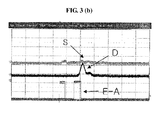
FIG. 3 (a) shows a slow light S and FIG. 3 (b) shows a routed light D based on nondegenerate four-wave mixing processes: Delayed optical switching/routing. The spatial direction of the output light S and D is determined by the phase matching conditions of the input light P, C, and A in FIG. 1.
FIG. 4 (a) illustrates a schematic diagram of a delayed optical logic gate, NOR, of the present invention. Letter DR stands for the delayed optical router comprised of a nonlinear optical medium 106 in FIG. 1, which is connected by optical waveguides, free space, or plasmon optical waveguide used for the laser beams P, C1, A, C2, B, S, D, X, and Y. FIG. 4 (b) illustrates the light pulse sequence.
FIG. 5 (a) illustrates a schematic diagram of a photon logic gate, AND, of the present invention. Letter DR stands for the delayed optical router comprised of a nonlinear optical medium 106 in FIG. 1, which is connected by optical waveguides, free space, or plasmon optical waveguide used for the laser beams P, C1, C2, A, B, S, D, X, and Y. FIG. 5 (b) illustrates the light pulse sequence.
FIG. 6 (a) illustrates a schematic diagram of a delayed optical logic gate, NAND/OR, of the present invention. Letter DR stands for the delayed optical router comprised of a nonlinear optical medium 106 in FIG. 1, which is connected by optical waveguides, free space, or plasmon optical waveguide used for the laser beams P, C1, C2, S, D, S1, D1, S2, D2, X, and Y. FIG. 6 (b) illustrates the light pulse sequence.
FIG. 7 (a) illustrates a schematic diagram of a delayed optical logic gate, NOR/XOR/AND, of the present invention. Letter DR stands for the delayed optical router comprised of a nonlinear optical medium 106 in FIG. 1, which is connected by optical waveguides, free space, or plasmon optical waveguide used for the laser beams P, C0, C1, C2, A, B, S, D, S1, D1, S2, D2, X, Y, and Z. FIG. 7 (b) illustrates the light pulse sequence.
DESCRIPTION OF THE PREFERRED EMBODIMENTS
To get a better understanding, reference is now made to the drawings which illustrate the preferred embodiments of the present invention.
FIG. 1 (a) shows a delayed optical router as a basic building block for the present invention of the delayed optical logic gates.
FIG. 1 (a) describes a delayed optical logic gate, NOT, where a single delayed optical router is used. Letters P, C, A, S, and D stand for light pulse at different propagation directions kP, kC, kA, kS, and kD, respectively. The numbers from 101 to 105 stand for lights as well as physical channels such as optical waveguide or free space used for the laser beams. The number 106 stands for a nonlinear optical medium. According to the delayed optical router, which will be explained below, the output S (104) is always OFF whenever the logical input light A (103) is switched ON, and vice versa. Here it should be noted that the light C may be continuous if the frequency of the light C is different from the light A. TABLE 1 shows the resulting Boolean algebra NOT of FIG. 1: The light C is always ON. Meanwhile, FIG. 1 (b) shows a pulse sequence.
TABLE 1
P A S (NOT) D
1 0 1 0
1 1 0 1
FIG. 2 (a) shows an energy level diagram of the nonlinear optical medium 106 of FIG. 1. The lower two closely spaced energy levels are resulted from the hyperfine splitting of most atoms or rare-earth doped crystals. The energy level structure of FIG. 2 (a) can also be obtained easily in semiconductor quantum wells or quantum dots utilizing heavy hole and light hole for exciton transitions or trion transitions. The nonlinear optical medium 106 of FIG. 1 has either three energy states; |1>, |2>, and |3> or four energy states; |1>, |2>, |3>, and |4>, where the level |4> is either virtual or real. The state |3> of FIG. 2 (a) is higher than |1> and |2> in energy. In fact the nonlinear optical medium 106 of FIG. 1 may have more than three energy levels, but only the mentioned energy levels shown in FIG. 2 (a) contribute to the photon logic mechanism of the present invention.
The output light D at frequency ωD is generated by nondegenerate four-wave mixing processes, where three laser interactions of P, C, and A are involved at frequencies ωP, ωC, ωA, respectively, with the nonlinear optical medium.
Similarly, the output light S at frequency ωS is generated by electromagnetically induced transparency (EIT) or coherent population oscillations (CPO) due to modified absorption and dispersion spectra: Refer S. E. Harris, Physical Review Letters, Vol. 64, pp. 1107-1110 (1991) for EIT, and R. Boyd et al., Science Vol. 301, pp. 200-202 (2003) for CPO.
The propagation directions of the light are shown in FIG. 2 (b), and are determined by the phase matching conditions, respectively: kD=kC−kP+kA. Here, the nondegenerate four-wave mixing generation is strongly enhanced owing to dark resonance or EIT: Harris in Physical Review Letters, Vol. 64, pp. 1107-1110 (1991); Jain et al. in Optics Letters Vol. 18, pp. 98-101 (1993); Ham et al. in Optics Letters, Vol. 22, pp. 1138-1140 (1997). Signal amplifications and high-conversion efficiency using atomic gases for nondegenerate four-wave mixing processes were also experimentally demonstrated by Hemmer at al. in Optics Letters, Vol. 20, pp. 982-984 (1995) and Jain et al. in Physical Review Letters, Vol. 77, pp. 4326-4329 (1996), respectively. The high-conversion efficiency of nondegenerate four-wave mixing processes was also experimentally demonstrated in ion-doped solids by Ham et al. in Physical Review A, Vol. 59, pp. R2583-2586 (1999). The enhancement of nondegenerate four-wave mixing processes is based on reduced first-order linear susceptibility and enhanced third-order nonlinear susceptibility owing to destructive and constructive quantum interference, respectively.
To show more detail relations between the input signal light P and the nondegenerate four-wave mixing output light D, coherence mapping should be understood. To see the coherence excitation in FIG. 2 (a), density matrix ρ must be discussed. The density matrix has been a useful tool to show a system's macroscopic ensemble; Quantum optics, Cambridge University Press, New York, N.Y. (1997), Edited by Scully and Zubairy.
In FIG. 2 (a), two laser beams C and P can induce two-photon coherence ρ12 on the transition |1>−|2> via the excited state |3>. The two-photon coherence is strongly enhanced if dark resonance or EIT involved. Here, dark resonance or EIT is the same physical phenomenon, but the term EIT roots in the absorption cancellation so that a resonant electromagnetic field can pass through an optically thick medium without experiencing any absorption. When coherent light A interacts with the nonlinear optical medium after the interaction for EIT, the two-photon coherence or dark resonance can be retrieved toward light P if the frequency of D is same as that of C: Ham et al, Opt. Lett. Vol. 22, pp. 1138-1140 (1997). Because coupling light C modifies the refractive index of the nonlinear optical medium 106 of FIG. 1 (a), the dispersion profile is also modified, so that the group velocity of the signal light P can be slowed down: Hau et al., Nature Vol. 397, pp. 594-598 (1999) and B. S. Ham et al., Phys. Rev. Lett. Vol. 88, p. 236024 (2002). The slow light is denoted by S. The light propagation vectors of the light P and S is same each other.
FIG. 3 (a) shows a slow light S and FIG. 3 (b) shows a routed light D observed in Pr3+:YSO based on FIG. 2 (a). This proves delayed nondegenerate four-wave mixing signal D, and the delayed light S can be used for delayed optical routing. E-P (E-A) stand for electric reference for P (A).
FIG. 4 (a) describes a delayed optical logic gate, i.e., NOR gate, where two-delayed optical routers are connected in series. Here, the output S (405) of the left (first) delayed optical router (DR1) is fed into the right (second) delayed optical router (DR2) as an input light (see P in FIG. 1 (a)). Two logical input light A (402) from DR1 and B (407) from DR2 perform optical logic inputs and result in Boolean algebra NOR at the output X (410). TABLE 2 shows the Boolean algebra of NOR resulted in the outputs X 410 by the combinations of two logic inputs A (402) and B (407). FIG. 4 (b) shows a pulse sequence.
TABLE 2
P A B S D X (NOR) Y
1 0 0 1 0 1 0
1 0 1 1 0 0 1
1 1 0 0 1 0 0
1 1 1 0 1 0 0
FIG. 5 (a) shows a delayed optical logic gate, i.e., AND gate, where the logic gate is composed of two delayed optical routers connected in series. Here, the output D (506) of the left delayed optical router DR1 (502) is fed into the right delayed optical router DR2 (507) as an input P (see P in FIG. 1 (a)). The combination of two logic input light A (503) from DR1 and B (508) from DR2 result in Boolean algebra AND to the output Y (511). TABLE 3 shows a resulting Boolean algebra AND appeared in the output Y (511) according to two logic inputs A (503) and B (508). FIG. 5 (b) shows a pulse sequence.
TABLE 3
P A B S D X Y (AND)
1 0 0 1 0 0 0
1 0 1 1 0 0 0
1 1 0 0 1 1 0
1 1 1 0 1 0 1
FIG. 6 (a) shows a delayed optical logic gate, i.e., NAND/OR gate. The system is composed of two-delayed optical routers connected in parallel, where the input light P (601) is shared. The output S1 (605) from the top delayed optical router DR1 and S2 (610) from the bottom delayed optical router DR2 is combined together to lead the logic output X (612). The outputs D1 (606) and D2 (611) are combined to lead the logic output Y (613). The signal light P (601) is split into two components through an optical splitter/combiner such as a Y branch or a beam splitter. Under the action of two inputs A (603) and B (608), the output logic X (612) and Y (613) perform Boolean logic operations NAND and OR, respectively: see TABLE 4. FIG. 6 (b) shows a pulse sequence.
TABLE 4
P A B S1 D1 S2 D2 X (NAND) Y (OR)
1 0 0 1 0 1 0 1 0
1 0 1 1 0 0 1 1 1
1 1 0 0 1 1 0 1 1
1 1 1 0 1 0 1 0 1
FIG. 7 (a) shows a delayed optical logic gate, i.e., NOR/XOR/AND gate. The system is composed of three delayed optical routers, where two of them are connected to the third one. Each output S (705) and D (706) of the delayed optical router DR0 is used as an input to the delayed optical routers DR1 and DR2, respectively. The output S1 (709) of the DR1 is used as a logic output X. The outputs D1 (710) and S2 (715) are combined together to lead the logic output Z (717). The output D2 (716) from the DR2 is used as a logic output Y. There are two logic inputs A (702) and B (708, 712), where A is for the DR0 and B is for both DR1 and DR2. As seen in TABLE 5, the two logic inputs A and B performs Boolean algebra NOR at the output X, XOR at Z, and AND at Y, simultaneously. FIG. 7 (b) shows a pulse sequence.
TABLE 5
X Y Z
S A B S D X D1 S2 Y (NOR) (AND) (XOR)
1 0 0 1 0 1 0 0 0 1 0 0
1 0 1 1 0 0 1 0 0 0 0 1
1 1 0 0 1 0 0 1 0 0 0 1
1 1 1 0 1 0 0 0 1 0 1 0
As the present invention may be embodied in several forms without departing from the spirit or essential characteristics thereof, it should also be understood that the above-described embodiments are not limited by any of the details of the foregoing description, unless otherwise specified, but rather should be construed broadly within its spirit and scope as defined in the appended claims, and therefore all changes and modifications that fall within the metes and bounds of the claims, or equivalence of such metes and bounds are therefore intended to be embraced by the appended claims.

Claims (2)

The invention claimed is:
1. A method for operating a logical gate using at least one or more delayed optical routers comprising a nonlinear optical medium, wherein the nonlinear optical medium comprises two closely spaced ground states such that a transition between the two ground states is dipole forbidden, and an excited state such that two-photon transitions between the two ground states via the excited state are allowed, the method comprising:
using at least one of a slow light (S) and a non-degenerate four-wave mixing signal (D) as a result of Boolean algebra,
wherein the slow light (S) is appeared by applying, to the nonlinear optical medium, a first laser beam (P) with a first frequency corresponding to a first transition between a first ground state of the two ground states and the excited state and a second laser beam (C) with a second frequency corresponding to a second transition between a second ground state of the two ground states and the excited state; and
the non-degenerate four-wave mixing signal (D) is appeared by applying, to the nonlinear optical medium, the first laser beam (P) with the first frequency, the second laser beam (C) with the second frequency and a third laser beam (A) with a third frequency corresponding to the second transition,
wherein the first laser beam (P) and the third laser beam (A) correspond to inputs of a Boolean NOT algebra, and the appearance or disappearance of the slow light (S) corresponds to a result of the Boolean NOT algebra.
2. An apparatus for an optical logic gate, comprising:
at least one or more delayed optical routers including at least one nonlinear optical medium, wherein the nonlinear optical medium comprises two closely spaced ground states such that a transition between the two ground states is dipole forbidden, and an excited state such that two-photon transitions between the two ground states via the excited state are allowed;
at least one port for outputting a result of the optical logic gate,
wherein the result is represented as at least one or more of a slow light (S) and a non-degenerate four-wave mixing signal (D),
the slow light (S) is appeared by applying, to the nonlinear optical medium, a first laser beam (P) with a first frequency corresponding to a first transition between a first ground state of the two ground states and the excited state and a second laser beam (C) with a second frequency corresponding to a second transition between a second ground state of the two ground states and the excited state; and
the non-degenerate four-wave mixing signal (D) is appeared by applying, to the nonlinear optical medium, the first laser beam (P) with the first frequency, the second laser beam (C) with the second frequency and a third laser beam (A) with a third frequency corresponding to the second transition,
wherein the first laser beam (P) and the third laser beam (A) correspond to inputs of a Boolean NOT algebra, and the appearance or disappearance of the slow light (S) corresponds to a result of the Boolean NOT algebra.
US14/729,840 2007-12-06 2015-06-03 Delayed optical logic gates for boolean algebra Active US9500933B2 (en)

Priority Applications (1)

Application Number Priority Date Filing Date Title
US14/729,840 US9500933B2 (en) 2007-12-06 2015-06-03 Delayed optical logic gates for boolean algebra

Applications Claiming Priority (9)

Application Number Priority Date Filing Date Title
KR1020070126381 2007-12-06
KR1020070126380 2007-12-06
KR1020070126380A KR100939246B1 (en) 2007-12-06 2007-12-06 Time-delayed optical router/switch and operation method thereof
KR1020070126381A KR100915171B1 (en) 2007-12-06 2007-12-06 Time-delayed optical logic gate and method for operating thereof
PCT/KR2007/006846 WO2009072693A1 (en) 2007-12-06 2007-12-26 Delayed optical logic gates
US28092308A 2008-08-27 2008-08-27
US13/014,344 US8259377B2 (en) 2007-12-06 2011-01-26 Delayed optical logic gates for boolean algebra
US13/560,644 US9075250B2 (en) 2007-12-06 2012-07-27 Delayed optical logic gates for boolean algebra
US14/729,840 US9500933B2 (en) 2007-12-06 2015-06-03 Delayed optical logic gates for boolean algebra

Related Parent Applications (1)

Application Number Title Priority Date Filing Date
US13/560,644 Division US9075250B2 (en) 2007-12-06 2012-07-27 Delayed optical logic gates for boolean algebra

Publications (2)

Publication Number Publication Date
US20150346581A1 US20150346581A1 (en) 2015-12-03
US9500933B2 true US9500933B2 (en) 2016-11-22

Family

ID=40717861

Family Applications (4)

Application Number Title Priority Date Filing Date
US12/280,923 Active US8259376B2 (en) 2007-12-06 2007-12-26 Delayed optical logic gates
US13/014,344 Active US8259377B2 (en) 2007-12-06 2011-01-26 Delayed optical logic gates for boolean algebra
US13/560,644 Expired - Fee Related US9075250B2 (en) 2007-12-06 2012-07-27 Delayed optical logic gates for boolean algebra
US14/729,840 Active US9500933B2 (en) 2007-12-06 2015-06-03 Delayed optical logic gates for boolean algebra

Family Applications Before (3)

Application Number Title Priority Date Filing Date
US12/280,923 Active US8259376B2 (en) 2007-12-06 2007-12-26 Delayed optical logic gates
US13/014,344 Active US8259377B2 (en) 2007-12-06 2011-01-26 Delayed optical logic gates for boolean algebra
US13/560,644 Expired - Fee Related US9075250B2 (en) 2007-12-06 2012-07-27 Delayed optical logic gates for boolean algebra

Country Status (3)

Country Link
US (4) US8259376B2 (en)
CN (1) CN101884181B (en)
WO (1) WO2009072693A1 (en)

Families Citing this family (7)

* Cited by examiner, † Cited by third party
Publication number Priority date Publication date Assignee Title
WO2009072693A1 (en) 2007-12-06 2009-06-11 Inha-Industry Partnership Institute Delayed optical logic gates
KR100939246B1 (en) * 2007-12-06 2010-02-02 인하대학교 산학협력단 Time-delayed optical router/switch and operation method thereof
CN103634048B (en) * 2013-03-08 2016-01-20 北方工业大学 N road light signal adjustable loop slower rays buffer shaper
CN106797254B (en) * 2014-11-12 2019-05-10 华为技术有限公司 A kind of device and method for realizing light logic
CN107493521B (en) * 2016-06-12 2022-08-02 中兴通讯股份有限公司 Signal sending method and device, signal receiving method and device, and signal transmission circuit
CN107976855B (en) * 2017-12-18 2023-09-22 北京大学 Universal linear optical all-optical logic gate and implementation method thereof
WO2020180885A1 (en) * 2019-03-03 2020-09-10 The University Of Chicago Coplanar superconductive millimeter-wave resonator with high kinetic inductance and associated methods

Citations (6)

* Cited by examiner, † Cited by third party
Publication number Priority date Publication date Assignee Title
US5757525A (en) 1996-06-05 1998-05-26 University Of Massachusetts All-optical devices
US6628453B2 (en) 2000-06-19 2003-09-30 Electronics And Telecommunications Research Institute Quantum switch
WO2008050938A1 (en) 2006-10-24 2008-05-02 Inha-Industry Partnership Institute Photon logic gates
US20080258049A1 (en) 2007-04-18 2008-10-23 Kuzmich Alexander M Quantum repeater using atomic cascade transitions
WO2009072694A1 (en) 2007-12-06 2009-06-11 Inha-Industry Partnership Institute Delayed optical router/switch
WO2009072693A1 (en) 2007-12-06 2009-06-11 Inha-Industry Partnership Institute Delayed optical logic gates

Family Cites Families (5)

* Cited by examiner, † Cited by third party
Publication number Priority date Publication date Assignee Title
CN1163788C (en) * 1998-04-24 2004-08-25 约翰霍普金斯大学 Optical method for quantum computing
US20030123516A1 (en) * 2001-10-15 2003-07-03 Steinberg Aephraim M. Quantum-interferometrically enhanced optical nonlinearities for photon switches and logic gates
JP4452070B2 (en) * 2003-12-04 2010-04-21 日本電信電話株式会社 Quantum computing device
CN1696809A (en) * 2005-01-27 2005-11-16 中山大学 Full optical logic gate of optic waveguide
CN1760744A (en) * 2005-11-10 2006-04-19 华中科技大学 Cascading structure of semiconductor optical amplifiers for realizing full optical logic AND gate and/or NOT gate

Patent Citations (12)

* Cited by examiner, † Cited by third party
Publication number Priority date Publication date Assignee Title
US5757525A (en) 1996-06-05 1998-05-26 University Of Massachusetts All-optical devices
US6628453B2 (en) 2000-06-19 2003-09-30 Electronics And Telecommunications Research Institute Quantum switch
WO2008050938A1 (en) 2006-10-24 2008-05-02 Inha-Industry Partnership Institute Photon logic gates
US20080258049A1 (en) 2007-04-18 2008-10-23 Kuzmich Alexander M Quantum repeater using atomic cascade transitions
WO2009072694A1 (en) 2007-12-06 2009-06-11 Inha-Industry Partnership Institute Delayed optical router/switch
WO2009072693A1 (en) 2007-12-06 2009-06-11 Inha-Industry Partnership Institute Delayed optical logic gates
US20100232001A1 (en) 2007-12-06 2010-09-16 Inha-Industry Partnership Institute Delayed optical logic gates
US20110116144A1 (en) 2007-12-06 2011-05-19 Byoung-Seung Ham Delayed optical logic gates
US8135277B2 (en) 2007-12-06 2012-03-13 Inha-Industry Partnership Institute Delayed optical router/switch
US8259376B2 (en) 2007-12-06 2012-09-04 Inha-Industry Partnership Institute Delayed optical logic gates
US8259377B2 (en) 2007-12-06 2012-09-04 Inha-Industry Partnership Institute Delayed optical logic gates for boolean algebra
US9075250B2 (en) * 2007-12-06 2015-07-07 Inha Industry Partnership Institute Delayed optical logic gates for boolean algebra

Non-Patent Citations (31)

* Cited by examiner, † Cited by third party
Title
Bigelow et al., "Superluminal and Slow Light Propagation in a Room-Temperature Solid", Science, vol. 301, No. 5630, Jul. 11, 2003, pp. 200-202, 3 pages.
Final Office Action dated Aug. 30, 2011, U.S. Appl. No. 12/280,923, filed Aug. 27, 2008, 21 pages.
Gauthier, et al., "Slow Light: From Basics to Future Prospects", Photonics Spectra, Mar. 2006, pp. 44-50, 6 pages.
Ham et al., "Efficient phase conjugation via two-photon coherence in an optically dense crystal", The American Physical Society, Physical Review A, vol. 59, No. 4, Apr. 1999, pp. R2583-R2586, 4 pages.
Ham et al., "Enhanced Nondegenerate Four-wave Mixing Owing to Electromagnetically Induced Transparency in a Spectral Hole-Burning Crystal", Optical Society of America, Optics Letters, vol. 22, No. 15, Aug. 1, 1997, pp. 1138-1140, 3 pages.
Ham, B.S., "Experimental demonstration of all-optical 1×2 quantum routing", Applied Physics Letters, vol. 85, Issue 6, Aug. 9, 2004, pp. 893-895, 3 pages.
Ham, B.S., "Population shelved all-optical modulation", Physical Review B, vol. 68, No. 7, Aug. 29, 2003, pp. 073102-1-1, 4 pages.
Hammer et al., "Efficient low-intensity optical phase conjugation based on coherent population trapping in sodium", The Optical Society of America, Optics Letters, vol. 20, No. 9, May 1, 1995, pp. 982-984, 3 pages.
Harris et al., "Nonlinear Optical Processes Using Electromagnetically Induced Transparency", The American Physical Society, Physical Review Letters, vol. 64, No. 10, Mar. 5, 1990, pp. 1107-1110, 4 pages.
Harris, Stephen E., "Electromagnetically Induced Transparency," Physics Today 50(7), Jul. 1997, pp. 36-42, 7 pages.
Harris, Stephen E., "Lasers without Inversion: Interfernce of Lifetime-Broadened Resonances", The American Physical Society, Physical Review Letters, vol. 62, No. 9, Feb. 27, 1989, pp. 1033-1036, 4 pages.
Hau et al., "Light speed reduction to 17 metres per second in an ultracold atomic gas", Macmillian Magazines Ltd., Nature, vol. 397, Feb. 18, 1999, pp. 594-598, 5 pages.
Jain et al., "Efficient Nonlinear Frequency Conversion with Maximal Atomic Coherence", The American Physical Society, Physical Review Letters, vol. 77, No. 21, Nov. 18, 1996, pp. 4326-4329, 4 pages.
Ku et al., "Slow light in semiconductor quantum wells", Optical Society of America, Optics Letters, vol. 29, No. 19, Oct. 1, 2004, pp. 2291-2293, 3 pages.
Notice of Allowance and Fee(s) Due dated Jan. 26, 2012, U.S. Appl. No. 12/280,923, filed Aug. 27, 2008, 11 pages.
Notice of Allowance and Fee(s) Due dated May 15, 2012, U.S. Appl. No. 12/280,923, filed Aug. 27, 2008, 11 pages.
Notice of Allowance and Fee(s) Due dated May 21, 2012, U.S. Appl. No. 13/014,344, filed Jan. 26, 2011, 15 pages.
Office Action dated Feb. 3, 2012, U.S. Appl. No. 13/014,344, filed Jan. 26, 2011, 23 pages.
Office Action dated Mar. 21, 2011, U.S. Appl. No. 12/280,923, filed Aug. 27, 2008, 16 pages.
Office Action Restriction dated Dec. 27, 2010, U.S. Appl. No. 12/280,923, filed Aug. 27, 2008, 5 pages.
Office Action Restriction dated Dec. 5, 2011, U.S. Appl. No. 13/014,344, filed Jan. 26, 2011, 11 pages.
Office Action Restriction dated May 12, 2011, U.S. Appl. No. 13/014,344, filed Jan. 26, 2011, 9 pages.
Response B to Office Action dated Nov. 29, 2011, U.S. Appl. No. 12/280,923, filed Aug. 27, 2008, 10 pages.
Response to Office Action dated Jun. 21, 2011, U.S. Appl. No. 12/280,923, filed Aug. 27, 2008, 13 pages.
Response to Office Action dated May 3, 2012, U.S. Appl. No. 13/014,344, filed Jan. 26, 2011, 12 pages.
Response to Office Action Restriction dated Jan. 26, 2011, U.S. Appl. No. 12/280,923, filed Aug. 27, 2008, 6 pages.
Response to Office Action Restriction dated Jan. 4, 2012, U.S. Appl. No. 13/014,344, filed Jan. 26, 2011, 12 pages.
Response to Office Action Restriction dated Jun. 22, 2011, U.S. Appl. No. 13/014,344, filed Jan. 26, 2011, 16 pages.
Totsuka et al., "Slow Light in Coupled-Resonator-Induced Transparency", The American Physical Society, Physical Review Letters, vol. 98, No. 21, May 25, 2007, p. 213904 1-4, 5 pages.
Turukhin et al., "Observation of Ultraslow and Stored Light Pulses in a Solid", The American Physical Society, Physical Review Letters, vol. 88, No. 2, Jan. 14, 2002, pp. 023602-01-023602-4, 4 pages.
Wu et al., "High-efficiency double phase conjugation in a Ce-doped strontium barium niobate crystal", Optical Society of America, Optics Letters, vol. 18, No. 2, Jan. 15, 1993, pp. 98-100, 3 pages.

Also Published As

Publication number Publication date
US20100232001A1 (en) 2010-09-16
US8259377B2 (en) 2012-09-04
US20120307327A1 (en) 2012-12-06
US20150346581A1 (en) 2015-12-03
US20110116144A1 (en) 2011-05-19
CN101884181A (en) 2010-11-10
US9075250B2 (en) 2015-07-07
WO2009072693A1 (en) 2009-06-11
CN101884181B (en) 2013-05-29
US8259376B2 (en) 2012-09-04

Similar Documents

Publication Publication Date Title
US9500933B2 (en) Delayed optical logic gates for boolean algebra
US7755821B2 (en) Photon logic gates
Taraphdar et al. Mach–Zehnder interferometer-based all-optical reversible logic gate
Burmeister et al. A comparison of optical buffering technologies
Wang et al. All-optical clocked flip-flops and binary counting operation using SOA-based SR latch and logic gates
Vagionas et al. Optical RAM and flip-flops using bit-input wavelength diversity and SOA-XGM switches
Singh et al. Interferometric architectures based all-optical logic design methods and their implementations
Kanellos et al. Bringing WDM into optical static RAM architectures
Maity et al. All-optical binary flip-flop with the help of terahertz optical asymmetric demultiplexer
US8135277B2 (en) Delayed optical router/switch
Ye et al. All-optical NAND gate using integrated SOA-based Mach–Zehnder interferometer
Islam Ultrafast switching with nonlinear optics
Chattopadhyay et al. Polarization-encoded all-optical quaternary multiplexer and demultiplexer–A proposal
Lowell et al. Application of slow light: a DARPA perspective
Mukherjee et al. A review on construction of logic gates by using soliton in all-optical communication system
KR100915171B1 (en) Time-delayed optical logic gate and method for operating thereof
Lv All-Optical Signal Processing in Ultrafast Optical Communication
Ma An investigation on all-optical multicast technology in all-optical networks
Bilich Optical Packet Switching With Photonic Crystals: An Overview
Ceipidor et al. Logic functions, devices, and circuits based on parametric nonlinear processes
Cherri et al. All-optical polarization-encoded negabinary signed-digit adder designs using terahertz-optical-asymmetric-demultiplexer switches
Campi et al. All-optical waveguide devices based on multiple quantum wells
Silberhorn et al. Integrated optical devices for quantum information applications
Ngah et al. Comparison of Interferometric all optical switches for router applications in OTDM systems
Notomi et al. On-chip all-optical processing based on photonic crystal nanocavities

Legal Events

Date Code Title Description
AS Assignment

Owner name: GWANGJU INSTITUTE OF SCIENCE AND TECHNOLOGY, KOREA

Free format text: ASSIGNMENT OF ASSIGNORS INTEREST;ASSIGNOR:HAM, BYOUNG SEUNG;REEL/FRAME:035779/0788

Effective date: 20150603

AS Assignment

Owner name: INHA INDUSTRY PARTNERSHIP INSTITUTE, KOREA, REPUBL

Free format text: CORRECTIVE ASSIGNMENT TO CORRECT THE ADD THE SECOND OMITTED RECEIVING PARTY DATA PREVIOUSLY RECORDED AT REEL: 035779 FRAME: 0788. ASSIGNOR(S) HEREBY CONFIRMS THE ASSIGNMENT;ASSIGNOR:HAM, BYOUNG SEUNG;REEL/FRAME:036502/0233

Effective date: 20150603

Owner name: GWANGJU INSTITUTE OF SCIENCE AND TECHNOLOGY, KOREA

Free format text: CORRECTIVE ASSIGNMENT TO CORRECT THE ADD THE SECOND OMITTED RECEIVING PARTY DATA PREVIOUSLY RECORDED AT REEL: 035779 FRAME: 0788. ASSIGNOR(S) HEREBY CONFIRMS THE ASSIGNMENT;ASSIGNOR:HAM, BYOUNG SEUNG;REEL/FRAME:036502/0233

Effective date: 20150603

STCF Information on status: patent grant

Free format text: PATENTED CASE

FEPP Fee payment procedure

Free format text: PAYOR NUMBER ASSIGNED (ORIGINAL EVENT CODE: ASPN); ENTITY STATUS OF PATENT OWNER: SMALL ENTITY

MAFP Maintenance fee payment

Free format text: PAYMENT OF MAINTENANCE FEE, 4TH YR, SMALL ENTITY (ORIGINAL EVENT CODE: M2551); ENTITY STATUS OF PATENT OWNER: SMALL ENTITY

Year of fee payment: 4

FEPP Fee payment procedure

Free format text: MAINTENANCE FEE REMINDER MAILED (ORIGINAL EVENT CODE: REM.); ENTITY STATUS OF PATENT OWNER: SMALL ENTITY