US9500930B1 - On-chip entangled photon source - Google Patents
On-chip entangled photon source Download PDFInfo
- Publication number
- US9500930B1 US9500930B1 US15/065,528 US201615065528A US9500930B1 US 9500930 B1 US9500930 B1 US 9500930B1 US 201615065528 A US201615065528 A US 201615065528A US 9500930 B1 US9500930 B1 US 9500930B1
- Authority
- US
- United States
- Prior art keywords
- wavelength
- photon
- cavity
- light
- photons
- Prior art date
- Legal status (The legal status is an assumption and is not a legal conclusion. Google has not performed a legal analysis and makes no representation as to the accuracy of the status listed.)
- Active
Links
- 230000010287 polarization Effects 0.000 claims abstract description 28
- 230000003287 optical effect Effects 0.000 claims description 82
- 239000000463 material Substances 0.000 claims description 23
- 238000000034 method Methods 0.000 claims description 20
- 230000005540 biological transmission Effects 0.000 claims description 19
- 239000004065 semiconductor Substances 0.000 claims description 18
- 239000000758 substrate Substances 0.000 claims description 14
- 239000002800 charge carrier Substances 0.000 claims 1
- 238000005516 engineering process Methods 0.000 abstract description 3
- 238000004891 communication Methods 0.000 description 11
- 238000010586 diagram Methods 0.000 description 5
- VYPSYNLAJGMNEJ-UHFFFAOYSA-N Silicium dioxide Chemical compound O=[Si]=O VYPSYNLAJGMNEJ-UHFFFAOYSA-N 0.000 description 4
- 239000000969 carrier Substances 0.000 description 3
- 230000004048 modification Effects 0.000 description 3
- 238000012986 modification Methods 0.000 description 3
- 229910052581 Si3N4 Inorganic materials 0.000 description 2
- 230000004075 alteration Effects 0.000 description 2
- 230000002238 attenuated effect Effects 0.000 description 2
- 239000000377 silicon dioxide Substances 0.000 description 2
- 241000321453 Paranthias colonus Species 0.000 description 1
- XUIMIQQOPSSXEZ-UHFFFAOYSA-N Silicon Chemical compound [Si] XUIMIQQOPSSXEZ-UHFFFAOYSA-N 0.000 description 1
- 238000010521 absorption reaction Methods 0.000 description 1
- 229910052681 coesite Inorganic materials 0.000 description 1
- 239000002131 composite material Substances 0.000 description 1
- 238000010276 construction Methods 0.000 description 1
- 229910052906 cristobalite Inorganic materials 0.000 description 1
- 230000001934 delay Effects 0.000 description 1
- 230000003111 delayed effect Effects 0.000 description 1
- 230000000694 effects Effects 0.000 description 1
- 238000004134 energy conservation Methods 0.000 description 1
- 239000000835 fiber Substances 0.000 description 1
- 239000003574 free electron Substances 0.000 description 1
- 230000003094 perturbing effect Effects 0.000 description 1
- 238000005086 pumping Methods 0.000 description 1
- 239000000523 sample Substances 0.000 description 1
- 229910052710 silicon Inorganic materials 0.000 description 1
- 239000010703 silicon Substances 0.000 description 1
- 235000012239 silicon dioxide Nutrition 0.000 description 1
- 230000003595 spectral effect Effects 0.000 description 1
- 229910052682 stishovite Inorganic materials 0.000 description 1
- 239000000126 substance Substances 0.000 description 1
- 229910052905 tridymite Inorganic materials 0.000 description 1
Images


Classifications
-
- G—PHYSICS
- G02—OPTICS
- G02F—OPTICAL DEVICES OR ARRANGEMENTS FOR THE CONTROL OF LIGHT BY MODIFICATION OF THE OPTICAL PROPERTIES OF THE MEDIA OF THE ELEMENTS INVOLVED THEREIN; NON-LINEAR OPTICS; FREQUENCY-CHANGING OF LIGHT; OPTICAL LOGIC ELEMENTS; OPTICAL ANALOGUE/DIGITAL CONVERTERS
- G02F1/00—Devices or arrangements for the control of the intensity, colour, phase, polarisation or direction of light arriving from an independent light source, e.g. switching, gating or modulating; Non-linear optics
- G02F1/35—Non-linear optics
- G02F1/3526—Non-linear optics using two-photon emission or absorption processes
-
- G—PHYSICS
- G02—OPTICS
- G02F—OPTICAL DEVICES OR ARRANGEMENTS FOR THE CONTROL OF LIGHT BY MODIFICATION OF THE OPTICAL PROPERTIES OF THE MEDIA OF THE ELEMENTS INVOLVED THEREIN; NON-LINEAR OPTICS; FREQUENCY-CHANGING OF LIGHT; OPTICAL LOGIC ELEMENTS; OPTICAL ANALOGUE/DIGITAL CONVERTERS
- G02F1/00—Devices or arrangements for the control of the intensity, colour, phase, polarisation or direction of light arriving from an independent light source, e.g. switching, gating or modulating; Non-linear optics
- G02F1/35—Non-linear optics
- G02F1/353—Frequency conversion, i.e. wherein a light beam is generated with frequency components different from those of the incident light beams
- G02F1/3536—Four-wave interaction
-
- G—PHYSICS
- G02—OPTICS
- G02F—OPTICAL DEVICES OR ARRANGEMENTS FOR THE CONTROL OF LIGHT BY MODIFICATION OF THE OPTICAL PROPERTIES OF THE MEDIA OF THE ELEMENTS INVOLVED THEREIN; NON-LINEAR OPTICS; FREQUENCY-CHANGING OF LIGHT; OPTICAL LOGIC ELEMENTS; OPTICAL ANALOGUE/DIGITAL CONVERTERS
- G02F1/00—Devices or arrangements for the control of the intensity, colour, phase, polarisation or direction of light arriving from an independent light source, e.g. switching, gating or modulating; Non-linear optics
- G02F1/35—Non-linear optics
- G02F1/39—Non-linear optics for parametric generation or amplification of light, infrared or ultraviolet waves
-
- H—ELECTRICITY
- H04—ELECTRIC COMMUNICATION TECHNIQUE
- H04L—TRANSMISSION OF DIGITAL INFORMATION, e.g. TELEGRAPHIC COMMUNICATION
- H04L9/00—Cryptographic mechanisms or cryptographic arrangements for secret or secure communications; Network security protocols
- H04L9/08—Key distribution or management, e.g. generation, sharing or updating, of cryptographic keys or passwords
- H04L9/0816—Key establishment, i.e. cryptographic processes or cryptographic protocols whereby a shared secret becomes available to two or more parties, for subsequent use
- H04L9/0852—Quantum cryptography
-
- G—PHYSICS
- G02—OPTICS
- G02F—OPTICAL DEVICES OR ARRANGEMENTS FOR THE CONTROL OF LIGHT BY MODIFICATION OF THE OPTICAL PROPERTIES OF THE MEDIA OF THE ELEMENTS INVOLVED THEREIN; NON-LINEAR OPTICS; FREQUENCY-CHANGING OF LIGHT; OPTICAL LOGIC ELEMENTS; OPTICAL ANALOGUE/DIGITAL CONVERTERS
- G02F2203/00—Function characteristic
- G02F2203/15—Function characteristic involving resonance effects, e.g. resonantly enhanced interaction
Definitions
- Quantum optics now finds applications in quantum communication, quantum computing, and quantum sensing.
- photon sources are used that are designed to emit a photon stream having a controlled number of photons.
- these sources rely on materials and structures that are difficult to implement in chip-scale integrated circuit devices.
- a photonic circuit comprises a narrowband laser that acts as a pumping source for a group of waveguide resonators.
- the laser emits light over a range of wavelengths and the light is received by two optical resonators each resonant at a different respective wavelength in the range of wavelengths and at a different respective polarization state.
- the two optical resonators output light in the two respective wavelengths to a four-wave mixing cavity that accommodates both orthogonal polarization states.
- the four-wave mixing cavity then outputs pairs of entangled photons, the pairs of entangled photons having respective third and fourth wavelengths with disparate polarization states that are entangled. Therefore, there are two degrees of freedom that are entangled between the photons of the two newly generated third and fourth wavelengths.
- the number of photons in the two wavelengths are equal and the polarization states of the two wavelengths are orthogonal and maximally entangled.
- the two polarization states are orthogonal, but there is a fifty percent chance that, for example, the third wavelength is horizontally polarized and the fourth wavelength is vertically polarized, and a fifty percent chance that the third wavelength is vertically polarized and the fourth wavelength is horizontally polarized.
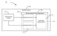
- FIG. 1 is a block diagram of an exemplary photonic circuit that facilitates generation of entangled photon pairs.
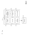
- FIG. 2 is a block diagram of an exemplary system that facilitates quantum communication via an on-chip heralded single-photon source.
- FIG. 3 is a block diagram of an exemplary system that facilitates quantum communication via an on-chip heralded single-photon source using an electro-optic modulator to control a transmitter output.
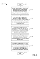
- FIG. 4 is a flow diagram that illustrates an exemplary methodology for outputting entangled photon pairs from an on-chip photon source.
- the term “or” is intended to mean an inclusive “or” rather than an exclusive “or.” That is, unless specified otherwise, or clear from the context, the phrase “X employs A or B” is intended to mean any of the natural inclusive permutations. That is, the phrase “X employs A or B” is satisfied by any of the following instances: X employs A; X employs B; or X employs both A and B.
- the articles “a” and “an” as used in this application and the appended claims should generally be construed to mean “one or more” unless specified otherwise or clear from the context to be directed to a singular form.
- the term “exemplary” is intended to mean serving as an illustration or example of something, and is not intended to indicate a preference.
- the system 100 includes a photonic circuit 102 that comprises an optical pump source 104 that emits light.
- the photonic circuit 102 further comprises an optical entanglement component 106 that comprises resonator cavities 108 - 110 and a four-wave mixing (FWM) cavity 112 , where the optical entanglement component 106 receives light emitted from the optical pump source 104 .
- the photonic circuit comprises a plurality of components deposited or installed on a same substrate.
- the term “on-chip” refers to a component or device deposited, installed upon, or comprising a substrate (e.g., a semi-conductor substrate).
- a substrate e.g., a semi-conductor substrate
- the same substrate comprises a silicon-based substance (e.g., silicon dioxide).
- the optical entanglement component 106 is optically coupled to the optical pump source 104 , and outputs pairs of quantum-entangled photons.
- the optical pump source 104 is an optical source that outputs light in a narrow band of wavelengths.
- the optical pump source 104 can emit light with a bandwidth of between 1-10 nanometers, with a bandwidth between 5 and 20 nanometers, with a bandwidth of 15-40 nanometers, with a bandwidth of 5-100 nanometers, etc.
- the optical pump source 104 can comprise a single-frequency laser that emits light with a highest intensity at a center wavelength (e.g., 1550 nm) and lower intensities at wavelengths on either side of the center wavelength.
- the optical pump source 104 can additionally include a doped fiber amplifier (DFA) that amplifies the light from the laser.
- DFA doped fiber amplifier
- an intensity of the light emitted by the optical pump source 104 can be on the order of 100 mW.
- the optical pump source 104 emits light in pulses. When the optical pump source 104 is excited to generate a pulse, photons are emitted according to some probability distribution.
- the power of the pump source 104 can be adjusted either to increase or decrease the probability of generating the third and the fourth wavelength photons via a four-wave mixing process. The probability to create the entangled photon pairs at the third and the fourth wavelengths follows the Poisson distribution.
- the probability of emitting one photon can be approximately 10%
- the probability of emitting two photons can be approximately 0.45%
- the probability of emitting zero photons can be approximately 90%, with a small probability of emitting some other number of photons.
- the optical pump source 104 is optically coupled to resonator cavities 108 - 110 .
- the first resonator cavity 108 is resonant at a first wavelength, ⁇ 1 , and at a first polarization state p 1
- the second resonator cavity 110 is resonant at a second wavelength ⁇ 2 , which is different from ⁇ 1 , and at a second polarization state p 2 orthogonal to p 1 .
- the wavelengths ⁇ 1 and ⁇ 2 are present in the light emitted from the optical pump source 104 .
- the first resonator cavity 108 When light enters the first resonator cavity 108 , light of the first resonant wavelength ⁇ 1 is amplified due to constructive interference while light of non-resonant wavelengths is attenuated due to losses in the first resonator cavity 108 . Similarly, when light enters the second resonator cavity 110 , light of the second resonant wavelength ⁇ 2 is amplified while light of non-resonant wavelengths is attenuated.
- the resonator cavities 108 - 110 therefore act as filters that pass light of their respective resonant wavelengths and polarization states. A resonant wavelength of a resonator cavity depends on parameters of its construction.
- the resonator cavities 108 - 110 can be ring resonators, and a resonant wavelength is based upon a diameter of the ring resonator.
- Resonator cavity 108 resonant at ⁇ 1 , receives the light from the optical pump source 104 and filters light at wavelengths other than ⁇ 1 .
- resonator cavity 110 receives the light from the pump source 104 and filters light at wavelengths other than ⁇ 2 .
- the resonator cavities 108 - 110 comprise optical ring resonators that are implemented as an arrangement of waveguides on a chip substrate.
- the resonator cavities 108 - 110 are each further optically coupled to the FWM cavity 112 , which is quadruply resonant at ⁇ 1 and ⁇ 2 , as well as additional wavelengths ⁇ s , and ⁇ i .
- the FWM cavity is a waveguide comprising an i-type semiconductor material, surrounded by an outer p-type semiconductor material and an inner n-type semiconductor material.
- a voltage is induced between the p-type material and the n-type material, free carriers in an optical cavity of the waveguide are absorbed by either the n-type or p-type material.
- the FWM cavity 112 receives light having the wavelength ⁇ 1 and the polarization p 1 from the first resonator cavity 108 , and also receives light having the wavelength ⁇ 2 and the polarization p 2 from the second resonator cavity 110 .
- the FWM cavity 112 comprises a material that exhibits a third-order optical nonlinearity under certain optical conditions.
- the FWM cavity 112 comprises a typical optical waveguide made with Si or Si 3 N 4 surrounded by SiO 2 that has a lower refractive index.
- Such Si or Si 3 N 4 material exhibits a third-order optical nonlinearity when a light with a sufficiently large intensity passes through.
- the third-order optical nonlinearity is the source for the FWM process.
- the FWM cavity 112 outputs polarization-entangled photons. Therefore, the polarization state of the composite quantum state of ⁇ s and ⁇ i is a maximally entangled state under the Bell polarization basis. Since the polarization states p s and p i are entangled, knowing one of the polarization states is sufficient to determine the other state.
- the entangled photons generated on-demand by the photonic circuit 102 can be used in a variety of applications.
- the entangled photons can be used in a heralded single-photon source in a quantum key distribution (QKD) transmitter.
- QKD quantum key distribution
- a transmitter that generates pairs of entangled photons and transmits only one photon of an entangled pair, two parties to communication can identify whether a transmission has been intercepted as part of a man-in-the-middle attack.
- a quantum computing device can perform computing operations based upon entangled photon pairs generated by the photonic circuit 102 .
- entangled photon pairs generated by the photonic circuit 102 can be used to perform quantum remote sensing, wherein entangled photon pairs can be used to probe a feature of interest remotely.
- an exemplary system 200 that facilitates quantum communication via an on-chip heralded single-photon source is illustrated.
- the BB84 communications protocol for example, is vulnerable to attack if multiple photons are transmitted in a single pulse. An attacker can intercept one of the photons and gain information without perturbing the remaining photons and thereby revealing her presence on the communications channel.
- the optical pump source 104 can emit pulses of varying numbers of photons according to a probabilistic distribution, the optical entanglement component 106 can emit more than one pair of photons for a single pulse of the optical pump source 104 .
- the system 200 includes a photonic circuit 202 that acts as a transmitter in a quantum communication system, and a quantum optical receiver 204 .
- the photonic circuit 202 and the quantum optical receiver 204 can communicate according to known quantum communications protocols such as, for example, the BB84 quantum key distribution (QKD) protocol.
- the quantum optical receiver 204 can be a photonic circuit or any other device capable of acting as a receiver in a quantum communication protocol.
- the photonic circuit 202 comprises the optical pump source 104 and the optical entanglement component 106 that outputs polarization-entangled photons as described above with respect to FIG. 1 .
- the optical pump source 104 as discussed above, emits light in pulses of varying numbers of photons, and the output of the optical entanglement component 106 comprises a correspondingly varying number of photons.
- the photonic circuit 202 further comprises a polarizing beam splitter 206 that receives the photons from the optical entanglement component 106 and diverts them along different paths according to their wavelength.
- Photons of a first wavelength say ⁇ s
- photon counter 208 while photons of a second wavelength, say ⁇ i , are diverted to a delay line 210 .
- the photon counter 208 counts a number of photons of the wavelength ⁇ s that it receives, while corresponding entangled photons of the wavelength ⁇ i are delayed by some amount of time via the delay line 210 before they are received at an optical modulator 212 .
- the optical entanglement component 106 outputs equal numbers of photons of respective orthogonal polarizations as a result of the conservation of energy and momentum in the FWM process.
- the number of photons of wavelength ⁇ s counted by the photon counter is equal to a number of polarization-entangled photons of wavelength ⁇ i that pass through the delay line 210 to the optical modulator 212 .
- the ⁇ s photons can therefore be said to “herald” the ⁇ i photons.
- the optical modulator 212 responsive to the photon counter 208 determining a number of ⁇ s photons received from the polarizing beam splitter 206 , can either block or pass on the photons of ⁇ i received from the polarizing beam splitter 206 via the delay line 210 .
- the amount of time by which the delay line 210 delays the ⁇ i photons depends upon a length of time needed for the photon counter 208 to determine a number of ⁇ s photons in the pulse.
- the optical modulator 212 is configured to block transmission of a pulse of photons when a number of corresponding entangled photons of the pulse received at the photon counter 208 is greater than one, and to allow transmission when the number of corresponding entangled photons received at the photon counter 208 is one.
- the optical modulator 212 comprises an acousto-optic modulator 212 that acts as a switch for the output of the photonic circuit 202 .
- FIG. 3 a system 300 in which the optical modulator 212 comprises an electro-optic modulator (EOM) 302 and a Mach-Zehnder interferometer 304 is illustrated.
- EOM electro-optic modulator
- the EOM 302 can modulate a phase of one of two input legs of the Mach-Zehnder interferometer 304 .
- the phase of the leg modulated by the EOM 302 is in phase with the other leg, the photon is passed to the receiver 204 .
- the phase of the leg modulated by the EOM 302 is out of phase with the other leg of the Mach-Zehnder interferometer 304 , the photons are not transmitted to the receiver 204 .
- the optical modulator 212 comprising the EOM 302 and the Mach-Zehnder modulator 304 also effectively operates as a switch on the output of the photonic circuit 202 .
- the optical modulator 212 allows the photonic circuit 202 to output a single photon at a time, even though the optical pump source 104 emits photons in varying numbers according to the probabilistic distribution.
- FIG. 4 illustrates an exemplary methodology relating to an on-chip entangled photon source. While the methodology is shown and described as being a series of acts that are performed in a sequence, it is to be understood and appreciated that the methodology is not limited by the order of the sequence. For example, some acts can occur in a different order than what is described herein. In addition, an act can occur concurrently with another act. Further, in some instances, not all acts may be required to implement a methodology described herein.
- the methodology 400 begins at 402 , and at 404 a first optical resonator receives light having a plurality of wavelengths that can be of varying intensities.
- the first optical resonator is deposited or installed on a semiconductor substrate.
- the first optical resonator is resonant at a first wavelength of light in the plurality of wavelengths.
- the light having the plurality of wavelengths is received at a second optical resonator that is deposited or installed on the same semiconductor substrate and that is resonant at a second wavelength in the plurality of wavelengths.
- light having the first wavelength is received from the first optical resonator at a FWM cavity that is also deposited or installed on the same semiconductor substrate.
- light having the second wavelength is received from the second optical resonator at the FWM cavity.
- the FWM cavity responsive to receiving the light having the first wavelength and the light having the second wavelength, the FWM cavity outputs at least one pair of polarization-entangled photons, whereupon the methodology 400 ends at 414 .
Landscapes
- Physics & Mathematics (AREA)
- Nonlinear Science (AREA)
- Engineering & Computer Science (AREA)
- General Physics & Mathematics (AREA)
- Optics & Photonics (AREA)
- Electromagnetism (AREA)
- Theoretical Computer Science (AREA)
- Computer Security & Cryptography (AREA)
- Computer Networks & Wireless Communication (AREA)
- Signal Processing (AREA)
- Optical Modulation, Optical Deflection, Nonlinear Optics, Optical Demodulation, Optical Logic Elements (AREA)
Abstract
Description
Claims (20)
Priority Applications (1)
| Application Number | Priority Date | Filing Date | Title |
|---|---|---|---|
| US15/065,528 US9500930B1 (en) | 2015-03-12 | 2016-03-09 | On-chip entangled photon source |
Applications Claiming Priority (2)
| Application Number | Priority Date | Filing Date | Title |
|---|---|---|---|
| US201562132100P | 2015-03-12 | 2015-03-12 | |
| US15/065,528 US9500930B1 (en) | 2015-03-12 | 2016-03-09 | On-chip entangled photon source |
Publications (1)
| Publication Number | Publication Date |
|---|---|
| US9500930B1 true US9500930B1 (en) | 2016-11-22 |
Family
ID=57287689
Family Applications (1)
| Application Number | Title | Priority Date | Filing Date |
|---|---|---|---|
| US15/065,528 Active US9500930B1 (en) | 2015-03-12 | 2016-03-09 | On-chip entangled photon source |
Country Status (1)
| Country | Link |
|---|---|
| US (1) | US9500930B1 (en) |
Cited By (7)
| Publication number | Priority date | Publication date | Assignee | Title |
|---|---|---|---|---|
| US20160147014A1 (en) * | 2014-11-25 | 2016-05-26 | The United States Of America As Represented By The Secretary Of The Navy | Embedded ring resonator-based photonic devices |
| US20190260478A1 (en) * | 2018-02-22 | 2019-08-22 | Kabushiki Kaisha Toshiba | Transmitter for a quantum communication system, a quantum communication system and a method of generating intensity modulated photon pulses |
| US20190376820A1 (en) * | 2018-06-07 | 2019-12-12 | U.S. Army Research Laboratory Attn: Rdrl-Loc-I | Methodology for in situ characterizing and calibrating an entangled photon distribution system |
| WO2021136632A1 (en) * | 2019-12-30 | 2021-07-08 | Asml Netherlands B.V. | Lithographic apparatus, metrology systems, illumination sources and methods thereof |
| WO2023219002A1 (en) * | 2022-05-12 | 2023-11-16 | 学校法人早稲田大学 | Quantum wavelength converter, heralded single photon source |
| WO2024123697A1 (en) * | 2022-12-05 | 2024-06-13 | University Of Maryland, College Park | Systems and methods for routing single photons from a trapped ion using a photonic integrated circuit |
| WO2025252217A1 (en) * | 2024-06-07 | 2025-12-11 | The Hong Kong University Of Science And Technology | On-chip photonic circuit for generating polarization-entangled photon-pairs |
Citations (7)
| Publication number | Priority date | Publication date | Assignee | Title |
|---|---|---|---|---|
| US7373059B2 (en) | 2006-09-22 | 2008-05-13 | Hewlett-Packard Development Company, L.P. | Compact, single chip-based, entangled polarization-state photon sources and methods for generating photons in entangled polarization states |
| US7570365B2 (en) | 2006-09-07 | 2009-08-04 | Magiq Technologies, Inc. | Compact tunable high-efficiency entangled photon source |
| US8717666B2 (en) | 2004-09-22 | 2014-05-06 | Quant-Viet Nguyen | Compact solid state entangled photon source |
| US20150117826A1 (en) * | 2013-10-31 | 2015-04-30 | President And Fellows Of Harvard College | Direct Entangled Triplet-Photon Sources And Methods For Their Design And Fabrication |
| US20150261058A1 (en) * | 2013-02-19 | 2015-09-17 | The University Of Bristol | Optical source |
| US9143266B2 (en) | 2011-07-14 | 2015-09-22 | The Trustees Of Columbia University On The City Of New York | Chip integrated single photon generation by active time multiplexing |
| US9268195B1 (en) * | 2013-09-11 | 2016-02-23 | Sandia Corporation | Methods and apparatus of entangled photon generation using four-wave mixing |
-
2016
- 2016-03-09 US US15/065,528 patent/US9500930B1/en active Active
Patent Citations (7)
| Publication number | Priority date | Publication date | Assignee | Title |
|---|---|---|---|---|
| US8717666B2 (en) | 2004-09-22 | 2014-05-06 | Quant-Viet Nguyen | Compact solid state entangled photon source |
| US7570365B2 (en) | 2006-09-07 | 2009-08-04 | Magiq Technologies, Inc. | Compact tunable high-efficiency entangled photon source |
| US7373059B2 (en) | 2006-09-22 | 2008-05-13 | Hewlett-Packard Development Company, L.P. | Compact, single chip-based, entangled polarization-state photon sources and methods for generating photons in entangled polarization states |
| US9143266B2 (en) | 2011-07-14 | 2015-09-22 | The Trustees Of Columbia University On The City Of New York | Chip integrated single photon generation by active time multiplexing |
| US20150261058A1 (en) * | 2013-02-19 | 2015-09-17 | The University Of Bristol | Optical source |
| US9268195B1 (en) * | 2013-09-11 | 2016-02-23 | Sandia Corporation | Methods and apparatus of entangled photon generation using four-wave mixing |
| US20150117826A1 (en) * | 2013-10-31 | 2015-04-30 | President And Fellows Of Harvard College | Direct Entangled Triplet-Photon Sources And Methods For Their Design And Fabrication |
Non-Patent Citations (7)
| Title |
|---|
| Azzini, et al., "Four-Wave Mixing and Generation of Correlated Photon Pairs in Silicon Ring Resonators and Photonic Molecules", In CLEO: 2013 Technical Digest, 2013 Optical Society of America, 2013, 2 pages. |
| Collins, et al., "Low Raman-Noise Correlated Photon-Pair Generation in a Dispersion-Engineered Chalcogenide As2S3 Planar Waveguide", In Optics Letters, vol. 37, No. 16, 2012 Optical Society of America, Aug. 15, 2012, pp. 3393-3395. |
| Engin, et al., "Photon Pair Generation in a Silicon Micro-Ring Resonator with Reverse Bias Enhancement", In Optical Express 27826, 2013 Optical Society of America, Nov. 6, 2013, 9 pages. |
| Horn, et al., "Monolithic Source of Photon Pairs", In Physical Review Letters PRL 108, 153605, 2012 American Physical Society, Apr. 13, 2012, pp. 153605-1-153605-5. |
| Jiang, et al., "A Silicon-Chip Source of Bright Photon-Pair Comb", 2012, pp. 1-29. |
| Kumar, et al., "Spectrally Multiplexed and Tunable-Wavelength Photon Pairs at 1.55um from a Silicon Coupled-Resonator Optical Waveguide", In Optics Letters, vol. 38, No. 16, 2013 Optical Society of America, Aug. 15, 2013, pp. 2969-2971. |
| Xiong, et al., "Slow-Light Enhanced Correlated Photon Pair Generation in a Silicon Photonic Crystal Waveguide", In Optics Letters, vol. 36, No. 17, 2011 Optical Society of America, Sep. 1, 2011, pp. 3413-3415. |
Cited By (14)
| Publication number | Priority date | Publication date | Assignee | Title |
|---|---|---|---|---|
| US20160147014A1 (en) * | 2014-11-25 | 2016-05-26 | The United States Of America As Represented By The Secretary Of The Navy | Embedded ring resonator-based photonic devices |
| US9709737B2 (en) * | 2014-11-25 | 2017-07-18 | The United States Of America As Represented By Secretary Of The Navy | Embedded ring resonator-based photonic devices |
| US20190260478A1 (en) * | 2018-02-22 | 2019-08-22 | Kabushiki Kaisha Toshiba | Transmitter for a quantum communication system, a quantum communication system and a method of generating intensity modulated photon pulses |
| US10951324B2 (en) * | 2018-02-22 | 2021-03-16 | Kabushiki Kaisha Toshiba | Transmitter for a quantum communication system, a quantum communication system and a method of generating intensity modulated photon pulses |
| US20190376820A1 (en) * | 2018-06-07 | 2019-12-12 | U.S. Army Research Laboratory Attn: Rdrl-Loc-I | Methodology for in situ characterizing and calibrating an entangled photon distribution system |
| US11009375B2 (en) * | 2018-06-07 | 2021-05-18 | The United States Of America As Represented By The Secretary Of The Army | Methodology for in situ characterizing and calibrating an entangled photon distribution system |
| WO2021136632A1 (en) * | 2019-12-30 | 2021-07-08 | Asml Netherlands B.V. | Lithographic apparatus, metrology systems, illumination sources and methods thereof |
| CN114902142A (en) * | 2019-12-30 | 2022-08-12 | Asml荷兰有限公司 | Lithographic apparatus, metrology system, illumination source and method thereof |
| US12124173B2 (en) | 2019-12-30 | 2024-10-22 | ASML Netherlands B.V. & ASML Holding N.V. | Lithographic apparatus, metrology systems, illumination sources and methods thereof |
| WO2023219002A1 (en) * | 2022-05-12 | 2023-11-16 | 学校法人早稲田大学 | Quantum wavelength converter, heralded single photon source |
| JP2023167667A (en) * | 2022-05-12 | 2023-11-24 | 学校法人早稲田大学 | Quantum wavelength converter, single photon source having messenger |
| JP7755308B2 (en) | 2022-05-12 | 2025-10-16 | 学校法人早稲田大学 | Quantum wavelength converter, single photon source with herald |
| WO2024123697A1 (en) * | 2022-12-05 | 2024-06-13 | University Of Maryland, College Park | Systems and methods for routing single photons from a trapped ion using a photonic integrated circuit |
| WO2025252217A1 (en) * | 2024-06-07 | 2025-12-11 | The Hong Kong University Of Science And Technology | On-chip photonic circuit for generating polarization-entangled photon-pairs |
Similar Documents
| Publication | Publication Date | Title |
|---|---|---|
| US9500930B1 (en) | On-chip entangled photon source | |
| US10158481B2 (en) | Apparatus and methods for quantum key distribution | |
| Stucki et al. | Continuous high speed coherent one-way quantum key distribution | |
| Liu et al. | Experimental demonstration of counterfactual quantum communication | |
| US9401766B2 (en) | Quantum communication network | |
| JP6760976B2 (en) | Chip-based quantum key distribution | |
| Tanaka et al. | High-speed quantum key distribution system for 1-Mbps real-time key generation | |
| US7242774B1 (en) | Quantum cryptography based on phase entangled photons | |
| US9143266B2 (en) | Chip integrated single photon generation by active time multiplexing | |
| Zbinden et al. | Practical aspects of quantum cryptographic key distribution | |
| CN106209361A (en) | A kind of still can ensure safe star-like quantum key distribution network without credible relaying | |
| Aldama et al. | Integrated QKD and QRNG photonic technologies | |
| US9465274B1 (en) | High-yield entangled single photon source | |
| Pinheiro et al. | Two-layer quantum key distribution | |
| Bacco et al. | Toward Fully‐Fledged Quantum and Classical Communication Over Deployed Fiber with Up‐Conversion Module | |
| Wang et al. | Multifunctional all-optical signal processing scheme for simultaneous multichannel WDM multicast and XOR logic gates based on FWM in QD-SOA | |
| JP2011182283A (en) | High-efficiency entangled photon pair swapping technique | |
| Bonfrate et al. | Asymmetric Mach-Zehnder germano-silicate channel waveguide interferometers for quantum cryptography systems | |
| Kleinert et al. | Hybrid photonic integrated circuits for quantum communications | |
| Nascimento et al. | Passive polarization and phase stabilization scheme for Twin-Field QKD | |
| Zhang et al. | High-speed phase-encoded quantum key distribution over a 1.4-km free-space channel | |
| Xavier et al. | Employing long fibre-optical Mach-Zehnder interferometers for quantum cryptography with orthogonal states | |
| Yicheng | Polarization-entangled quantum key distribution over telecommunication fibres | |
| Tunsiri et al. | Optical-quantum security using dark-bright soliton conversion in a ring resonator system | |
| Rogers | Components for Broadband QKD |
Legal Events
| Date | Code | Title | Description |
|---|---|---|---|
| AS | Assignment |
Owner name: U.S. DEPARTMENT OF ENERGY, DISTRICT OF COLUMBIA Free format text: CONFIRMATORY LICENSE;ASSIGNOR:SANDIA CORPORATION;REEL/FRAME:038746/0998 Effective date: 20160411 |
|
| AS | Assignment |
Owner name: SANDIA CORPORATION, NEW MEXICO Free format text: ASSIGNMENT OF ASSIGNORS INTEREST;ASSIGNORS:BISSON, SCOTT E.;SOH, DANIEL B.S.;SIGNING DATES FROM 20160414 TO 20160627;REEL/FRAME:040005/0009 |
|
| STCF | Information on status: patent grant |
Free format text: PATENTED CASE |
|
| AS | Assignment |
Owner name: NATIONAL TECHNOLOGY & ENGINEERING SOLUTIONS OF SAN Free format text: CHANGE OF NAME;ASSIGNOR:SANDIA CORPORATION;REEL/FRAME:047052/0538 Effective date: 20170501 |
|
| MAFP | Maintenance fee payment |
Free format text: PAYMENT OF MAINTENANCE FEE, 4TH YEAR, LARGE ENTITY (ORIGINAL EVENT CODE: M1551); ENTITY STATUS OF PATENT OWNER: LARGE ENTITY Year of fee payment: 4 |
|
| MAFP | Maintenance fee payment |
Free format text: PAYMENT OF MAINTENANCE FEE, 8TH YEAR, LARGE ENTITY (ORIGINAL EVENT CODE: M1552); ENTITY STATUS OF PATENT OWNER: LARGE ENTITY Year of fee payment: 8 |