US9500911B2 - Liquid crystal display panel - Google Patents
Liquid crystal display panel Download PDFInfo
- Publication number
- US9500911B2 US9500911B2 US14/488,492 US201414488492A US9500911B2 US 9500911 B2 US9500911 B2 US 9500911B2 US 201414488492 A US201414488492 A US 201414488492A US 9500911 B2 US9500911 B2 US 9500911B2
- Authority
- US
- United States
- Prior art keywords
- spacers
- spacer
- liquid crystal
- substrate
- diameter
- Prior art date
- Legal status (The legal status is an assumption and is not a legal conclusion. Google has not performed a legal analysis and makes no representation as to the accuracy of the status listed.)
- Active, expires
Links
Images


Classifications
-
- G—PHYSICS
- G02—OPTICS
- G02F—OPTICAL DEVICES OR ARRANGEMENTS FOR THE CONTROL OF LIGHT BY MODIFICATION OF THE OPTICAL PROPERTIES OF THE MEDIA OF THE ELEMENTS INVOLVED THEREIN; NON-LINEAR OPTICS; FREQUENCY-CHANGING OF LIGHT; OPTICAL LOGIC ELEMENTS; OPTICAL ANALOGUE/DIGITAL CONVERTERS
- G02F1/00—Devices or arrangements for the control of the intensity, colour, phase, polarisation or direction of light arriving from an independent light source, e.g. switching, gating or modulating; Non-linear optics
- G02F1/01—Devices or arrangements for the control of the intensity, colour, phase, polarisation or direction of light arriving from an independent light source, e.g. switching, gating or modulating; Non-linear optics for the control of the intensity, phase, polarisation or colour
- G02F1/13—Devices or arrangements for the control of the intensity, colour, phase, polarisation or direction of light arriving from an independent light source, e.g. switching, gating or modulating; Non-linear optics for the control of the intensity, phase, polarisation or colour based on liquid crystals, e.g. single liquid crystal display cells
- G02F1/133—Constructional arrangements; Operation of liquid crystal cells; Circuit arrangements
- G02F1/1333—Constructional arrangements; Manufacturing methods
- G02F1/1339—Gaskets; Spacers; Sealing of cells
- G02F1/13394—Gaskets; Spacers; Sealing of cells spacers regularly patterned on the cell subtrate, e.g. walls, pillars
-
- G—PHYSICS
- G02—OPTICS
- G02F—OPTICAL DEVICES OR ARRANGEMENTS FOR THE CONTROL OF LIGHT BY MODIFICATION OF THE OPTICAL PROPERTIES OF THE MEDIA OF THE ELEMENTS INVOLVED THEREIN; NON-LINEAR OPTICS; FREQUENCY-CHANGING OF LIGHT; OPTICAL LOGIC ELEMENTS; OPTICAL ANALOGUE/DIGITAL CONVERTERS
- G02F1/00—Devices or arrangements for the control of the intensity, colour, phase, polarisation or direction of light arriving from an independent light source, e.g. switching, gating or modulating; Non-linear optics
- G02F1/01—Devices or arrangements for the control of the intensity, colour, phase, polarisation or direction of light arriving from an independent light source, e.g. switching, gating or modulating; Non-linear optics for the control of the intensity, phase, polarisation or colour
- G02F1/13—Devices or arrangements for the control of the intensity, colour, phase, polarisation or direction of light arriving from an independent light source, e.g. switching, gating or modulating; Non-linear optics for the control of the intensity, phase, polarisation or colour based on liquid crystals, e.g. single liquid crystal display cells
- G02F1/133—Constructional arrangements; Operation of liquid crystal cells; Circuit arrangements
- G02F1/1333—Constructional arrangements; Manufacturing methods
- G02F1/1339—Gaskets; Spacers; Sealing of cells
- G02F1/13398—Spacer materials; Spacer properties
-
- G02F2001/13398—
Definitions
- the present invention relates to a liquid crystal display panel, and in particular, to a liquid crystal display panel in which a liquid crystal gap is secured by arranging spacers between transparent substrates.
- LCDs Liquid crystal display panels
- PDAs personal digital assistants
- multimedia players are used as display devices of a variety of portable information devices such as cellular phones, personal digital assistants (PDAs), digital cameras and multimedia players.
- the liquid crystal display panel comprises a liquid crystal encapsulated between a pair of transparent substrates made of glass, resin or the like and performs the image display by driving and controlling the liquid crystal molecules by use of an electric field.
- One of the transparent substrates is used as an array substrate having a surface on which a plurality of thin-film transistors (TFTs) are arranged in an array.
- the other transparent substrate is used as a color filter substrate having a surface on which a black matrix (BM) and color filters are arranged.
- BM black matrix
- the low-temperature bubble defects are display defects caused by vacuum bubbles (low-temperature bubbles) forming in the liquid crystal layer when the substrate distance cannot change smoothly following the volume contraction of the liquid crystal in a low-temperature environment.
- the unevenness in brightness by pressure is a display defect occurring in regions of the liquid crystal display panel where the substrate distance has become nonuniform due to external pressure locally applied to a surface of a transparent substrate.
- JP-A-2002-341354, JP-A-2003-84289, and JP-A-2003-121857 have been disclosed in JP-A-2002-341354, JP-A-2003-84289, and JP-A-2003-121857.
- the low-temperature bubble defects are prevented by allowing the substrate distance to decrease flexibly due to elastic deformation of the higher spacers.
- the unevenness in brightness by pressure is prevented by inhibiting excessive decrease in the substrate distance by having both the higher spacers and the lower spacers receive the applied load.
- the pixel aperture ratio is the area ratio between one pixel region of the liquid crystal and a region in the one pixel region effective for the displaying (region other than ineffective parts such as the BM). Therefore, how to reduce the area of the BM regions is especially important in order to achieve a sufficient pixel aperture ratio in a high-definition liquid crystal display panel.
- the spacers are generally formed in the BM regions.
- the spacers are arranged at intersecting parts of the lattice-shaped BM (at the corner positions of the pixels). Even the most miniaturized spacer is in a size of approximately ⁇ 10 ⁇ m at present. In liquid crystal display panels having resolution within 400 ppi, a sufficient pixel aperture ratio can be achieved even if a BM region of a size over 20 ⁇ m ⁇ 15 ⁇ m is formed between adjoining intersecting parts of the lattice, and thus spacers larger than ⁇ 10 ⁇ m can be arranged in the BM regions.
- the formation of multiple types of spacers differing in the height is carried out generally by use of a multi-tone mask.
- the multi-tone mask (gray-tone mask, half-tone mask, etc.) is a mask having not only regions of 0% transmittance and regions of 100% transmittance but also regions of intermediate transmittance.
- a liquid crystal display panel has the following characteristic features:
- a liquid crystal display panel comprising a plurality of spacers arranged between a pair of transparent substrates and a liquid crystal encapsulated between the transparent substrates, the spacers are of a uniform height and each spacer is substantially in a trapezoidal shape in which the ratio between the top area and the bottom area is 0.3 or less.
- the spacers are arranged at appropriate density so that the contact area ratio of the spacers' top surfaces in contact with one of the transparent substrates per unit area is within a range of 0.8%-1.0%.
- each spacer arranged between the transparent substrates substantially in a trapezoidal shape in which the ratio between the top area and the bottom area is 0.3 or less according to the present invention, both the prevention of the low-temperature bubble defects and the prevention of the unevenness in brightness by pressure can be achieved while using spacers of a uniform height.
- FIG. 1 is a vertical sectional view for explaining an embodiment of a liquid crystal display panel in accordance with the present invention.
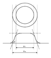
- FIG. 2 is a schematic diagram for explaining a top diameter and a bottom diameter of a spacer.
- FIG. 3 is a graph showing the relationship between the load applied to each columnar spacer and the indentation depth.
- FIG. 4 is a table showing the number of columnar spacers necessary for achieving a prescribed withstand load.
- FIG. 5 is a graph showing the relationship between the applied load and the indentation depth in regard to spacers according to an example (1) and comparative examples (1) and (2).
- FIG. 6 is a table showing the result of evaluation of light leakage in regard to the spacers according to the example (1) and the comparative examples (1) and (2).
- FIG. 7 is a table showing the result of evaluation of spacers according to examples (2)-(5) and comparative examples (3)-(6).
- FIG. 1 is a vertical sectional view for explaining an embodiment of a liquid crystal display panel in accordance with the present invention.
- the liquid crystal display panel shown in FIG. 1 is characterized in that in a liquid crystal display panel comprising a plurality of spacers 14 arranged between a pair of transparent substrates 11 and 12 and a liquid crystal 13 encapsulated between the transparent substrates, the spacers 14 are of a uniform height and each spacer 14 is substantially in a trapezoidal shape in which the ratio between the top area and the bottom area is 0.3 or less.
- the transparent substrates 11 and 12 are made of transparent material such as glass or resin.
- One of the transparent substrates 11 and 12 is used as an array substrate having a substrate surface on which an array of TFTs is arranged.
- the other substrate is used as a color filter substrate having a substrate surface on which a BM (Black Matrix) and color filters are arranged.
- the transparent substrate 11 is used as the array substrate and the transparent substrate 12 is used as the color filter substrate.
- alignment layers for setting the alignment (orientation) of the liquid crystal molecules 13 between the transparent substrates 11 and 12 are formed on the opposing surfaces of the transparent substrates 11 and 12 .
- the rubbing treatment has been performed on the alignment layers in order to provide the alignment layers with the alignment function.
- a plurality of spacers 14 of a uniform height are arranged between the pair of transparent substrates 11 and 12 . While the spacers 14 are arranged in the BM regions of the transparent substrate 12 (color filter substrate) in this embodiment, it is also possible to arrange the spacers 14 on the transparent substrate 11 (array substrate). In this case, the spacers 14 are desired to be arranged in regions facing the BM regions.
- Each of the spacers 14 is in a trapezoidal shape in which the top area is smaller than the bottom area.
- a spacer in the shape of a circular truncated cone (frustum of a circular cone), having a circular cross-sectional shape along a substrate plane, is used as each spacer 14 .
- Such a trapezoidal spacer 14 having a thin tip end part, is characterized in that the spacer is easily deformed (soft) while the load in the direction for crushing (flattening out) the spacer 14 (load in the direction for narrowing the distance between the transparent substrates 11 and 12 ) is low.
- the spacers 14 are easily deformed, allowing the distance between the transparent substrates 11 and 12 to change smoothly following the volume contraction of the liquid crystal 13 . This is effective for preventing the low-temperature bubble defects which occur when the substrate distance cannot smoothly follow the volume contraction of the liquid crystal 13 in a low-temperature environment.
- the trapezoidal spacer 14 gradually thickening toward the bottom, is characterized in that the spacer becomes hard to deform (hardens) with the increase in the load in the direction for crushing (flattening out) the spacer 14 .
- the withstand load of the trapezoidal spacers 14 increases and the function of maintaining the distance between the transparent substrates 11 and 12 strengthens. This is effective for preventing the unevenness in brightness by pressure which occurs when the substrate distance becomes nonuniform due to external pressure locally applied to a substrate surface.
- the above characteristics of the trapezoidal spacer 14 (the deformation is large (soft) at light loads but decreases (hardens) with the increase in the load) vary depending on the ratio between the top area and the bottom area in the trapezoidal shape.
- the above characteristics were achieved in good balance that is effective for both the prevention of the low-temperature bubble defects and the prevention of the unevenness in brightness by pressure when the ratio between the top area and the bottom area was 0.3 or less.
- the prevention of the low-temperature bubble defects and the prevention of the unevenness in brightness by pressure were both achieved successfully while using spacers of a uniform height.
- the achievement of both the prevention of the low-temperature bubble defects and the prevention of the unevenness in brightness by pressure was impossible unless spacers of different heights were used in combination.
- the spacer 14 in this embodiment may also be in a trapezoidal shape other than the aforementioned circular truncated cone shape.
- a spacer in the shape of a truncated pyramid frustum of a pyramid
- a spacer in a trapezoidal shape having rounded top and bottom as shown in FIG. 2 (explained later) is also usable as each spacer 14 in the present invention.
- the inclined part of the spacer 14 between the top and the bottom may also be formed in a step-like shape, for example.
- substantially in a trapezoidal shape” in the present invention means that such a variety of trapezoidal shapes are possible.
- spacers 14 that are substantially in trapezoidal shapes in which the ratio between the top area and the bottom area is a prescribed value or less are used in the present invention, by which both the prevention of the low-temperature bubble defects and the prevention of the unevenness in brightness by pressure can be achieved successfully while using spacers of a uniform height. In other words, it is unnecessary to form multiple types of spacers differing in the height for the purpose of achieving both the prevention of the low-temperature bubble defects and the prevention of the unevenness in brightness by pressure.
- the spacers 14 are especially desirable to arrange the spacers 14 at appropriate density so that the contact area ratio of the spacers' top surfaces in contact with one of the transparent substrates 11 and 12 (the transparent substrate 11 (array substrate) in this embodiment) per unit area is within a prescribed range. With this configuration, the function of preventing the low-temperature bubble defects and the unevenness in brightness by pressure can be achieved more effectively.
- FIG. 2 show a plan view and a side view of the spacer 14 , respectively.
- the actual spacer 14 is not in a perfect trapezoidal shape but in a slightly rounded trapezoidal shape.
- the inclination angle of the lateral surface of the spacer 14 gradually increases to ⁇ , thereafter remains at ⁇ for a while (forming an inclined surface at the inclination angle ⁇ ), and thereafter gradually decreases till the lateral surface reaches the planar top surface.
- intersection points of the substrate surface and imaginary lines at the inclination angle ⁇ extending along the inclined surface of the spacer 14 are regarded as the boundary of the bottom surface, and the bottom area is calculated on the basis of the result of measurement of the diameter of the bottom surface's boundary (bottom diameter ⁇ B).
- intersection points of the above imaginary lines and a plane including the top surface of the spacer 14 are regarded as the boundary of the top surface, and the top area is calculated based on the result of measurement of the diameter of the top surface's boundary (top diameter ⁇ T).
- An area ratio between the top surface and the bottom surface is defined as ( ⁇ T) 2 /( ⁇ B) 2 .
- the calculation of the top area can be performed by use of the uppermost trapezoidal part, and the calculation of the bottom area can be performed by use of the lowermost trapezoidal part.
- the trapezoidal spacers 14 also have the following advantages in addition to the effectiveness for the prevention of the low-temperature bubble defects and the unevenness in brightness by pressure:
- the trapezoidal spacers 14 Compared to columnar spacers, the trapezoidal spacers 14 less obstruct the rubbing treatment.
- the orientation is given to the alignment layer on each substrate surface by rubbing the alignment layer with cloth in a prescribed direction.
- the inclined surfaces of the trapezoidal spacers 14 are not steep but at a gentle angle, and thus the cloth easily reaches the inside parts around the roots of the spacers compared to the cases of columnar spacers and the rubbing can be performed sufficiently to the inside parts around the roots of the spacers 14 .
- the orientation can be appropriately given also to the regions in the vicinity of the spacers 14 and the orientation of the liquid crystal molecules can be aligned uniformly.
- This makes it possible to reduce the area of the BM regions (for taking care of the light leakage caused by disturbance in the liquid crystal molecule orientation) compared to cases where columnar spacers of the same installation area are used. Consequently, the pixel aperture ratio can be increased and high transmittance and high luminance can be secured excellently even in high-definition liquid crystal display panels. This leads to the quality improvement of liquid crystal display panels.
- the multi-tone mask for creating the difference in the height becomes unnecessary. Since the spacers 14 can be produced by use of a single-tone mask which is cheaper than the multi-tone mask, the cost for the mask used for producing the spacers can be reduced.
- the adjustment of the withstand load of the spacers 14 can be made by increasing/decreasing the amount of exposure (light exposure) in the production of the spacers, it is unnecessary to change the single-tone mask for the adjustment of the withstand load.
- the withstand load of produced spacers differ from expectation (intended value)
- the increasing/decreasing of the amount of exposure causes the change of diameter to both the higher spacers and the lower spacers.
- the adjustment of the withstand load by just increasing/decreasing the amount of exposure is difficult and it often becomes necessary to remake the mask.
- the mask remaking cost can be reduced according to this embodiment compared to cases where multiple types of spacers differing in the height are formed.
- a commonly-used negative-type acrylic resin material was used for the production of the columnar spacers.
- a commonly-used negative-type acrylic resin material when radicals (unpaired electrons) are generated due to the photolysis of a polymerization initiator, radical polymerization occurs between double bonds of the acrylic resin and double bonds of an acrylic crosslinking agent. Accordingly, the molecular weight increases and a pattern is formed due to insolubilization against the developing solution.
- a spacer pattern was formed by applying the negative-type material on the surface of a substrate, light-exposing the substrate via a mask having openings corresponding to the parts to be left as the spacers, performing the development by using an alkaline developing solution, and rinsing the substrate (having the developed pattern thereon) with pure water. Thereafter, the substrate with the spacer pattern was heated in an oven at 230° C. for 30 minutes to promote the crosslinking reaction and increase the strength, by which the spacers were completed.
- the method of the production of the trapezoidal spacers is basically equivalent to that of the columnar spacers, and thus the difference from the production of the columnar spacers will be explained below.
- the spacer pattern was formed while reducing the crosslinking reaction to a minimum, by shortening the development time and adjusting the amount of exposure to the lower limit allowing for the patterning. Thereafter, the dimensional difference between the top diameter and the lower diameter was created by reflowing the spacer pattern by quickly heating the substrate on a hot plate heated at 150° C. in the oven. The fine adjustment of the dimensional difference was made by adjusting the amount of exposure and the development time.
- Each panel for the evaluation was completed by performing the rubbing treatment on a 5-inch full HD array substrate (the number of pixels: 1920 ⁇ 1080, 438 ppi) and a color filter substrate of the same size (having spacers formed thereon so that the spacer shape and the contact area differ from substrate to substrate), bonding the array substrate and the color filter substrate together by using a sealing material, and encapsulating the liquid crystal between the substrates.
- the panels By using the panels, the presence/absence of the low-temperature bubble defects and the presence/absence of the unevenness in brightness by pressure were evaluated.
- the array substrates and the color filter substrates were produced by standard methods, and thus detailed explanation thereof is omitted for brevity.
- Evaluation of the light leakage was also carried out by using cells each produced by forming spacers on a glass substrate at positions corresponding to the corners of the 5-inch full HD pixels, performing the rubbing treatment on the substrate, bonding the substrate to another glass substrate that has undergone the rubbing treatment in the same way, and encapsulating the liquid crystal between the substrates.
- the top diameter, the bottom diameter and the height of the spacers were measured by using a laser microscope.
- the top area and the bottom area can be calculated through the measurement of the top diameter the bottom diameter.
- the load deformation was measured by using a Fischerscope (micro hardness tester) and a 25 ⁇ m 2 plane indenter.
- Each cell was formed by arranging an array substrate, a liquid crystal layer and a color filter substrate from the bottom. Two polarizing plates were arranged to sandwich the cell. The maximum luminance value (white luminance) and the minimum luminance value (black luminance) were measured by arranging a back light at the bottom (under the array substrate), arranging a luminance meter at the top (over the color filter substrate), and rotating one of the polarizing plates.
- Each panel for the evaluation was left at ⁇ 20° C. for 24 hours.
- An impact was put on the panel in the ⁇ 20° C. state by dropping a metallic ball (pachinko ball) onto the center of the panel from a position 10 cm above.
- a metallic ball piachinko ball
- visual observation was carried out to check the presence/absence of the formation of bubbles.
- a load of 150 N was applied onto the evaluation panel at 5-minute intervals for a total of 50 times by using a metallic bar having a ⁇ 10 mm plane tip end. Thereafter, visual observation was conducted to check the presence/absence of indentations.
- the produced columnar spacers had five column diameters (top diameters in this example) of 9.7 ⁇ m, 4.9 ⁇ m, 4.0 ⁇ m, 3.2 ⁇ m and 2.1 ⁇ m.
- the height of each spacer was set constant at 4 ⁇ m.
- the difference between the bottom diameter and the top diameter of each spacer was 1.5 ⁇ m.
- FIG. 3 is a graph showing the result of the measurement of the load applied to each columnar spacer and the indentation depth by use of the Fischerscope.
- the vertical axis represents the load (mN) and the horizontal axis represents the indentation depth ( ⁇ m). Load deformation curves indicating the relationship between the applied load and the indentation depth are shown.
- the load deformation curves include a load deformation curve 21 in the case where the column diameter was 9.7 ⁇ m, a load deformation curve 22 in the case where the column diameter was 4.9 ⁇ m, a load deformation curve 23 in the case where the column diameter was 4.0 ⁇ m, a load deformation curve 24 in the case where the column diameter was 3.2 ⁇ m, and a load deformation curve 25 in the case where the column diameter was 2.1 ⁇ m.
- Each load deformation curve 21 - 25 indicates the result of the measurement of the indentation depth (deformation) along the passage of time (indicated by the arrows) in a process of gradually increasing the load applied to the columnar spacer, maintaining the applied load at 10 mN for a while (e.g., 5 seconds), and thereafter gradually reducing the applied load.
- the spacer of the largest column diameter (corresponding to the load deformation curve 21 ) exhibited a small deformation of approximately 0.2 ⁇ m even with the 10 mN load and quickly returned to the original shape after the load was removed.
- the load deformation increased and the time necessary for returning from the deformed shape to the original shape after the removal of the load also increased.
- FIG. 4 is a table showing the result of evaluation of the number of columnar spacers necessary for achieving a prescribed withstand load.
- the spacer having the 9.7 ⁇ m column diameter produced by use of a mask having openings 11 ⁇ m in diameter
- the reference spacer the number of columnar spacers (having a column diameter other than 9.7 ⁇ m) necessary for achieving a withstand load equivalent to that of the reference spacer was evaluated.
- the column area (the area of a plane cross section) of the reference spacer (column diameter: 9.7 ⁇ m) was 73.9 ⁇ m 2 and the deformation caused by applying the 10 mN load onto one reference spacer was 0.20 ⁇ m.
- the spacer having the 4.9 ⁇ m column diameter (produced by use of a mask having openings 6 ⁇ m in diameter) had a column area of 18.9 ⁇ m 2 .
- the deformation of the spacers caused by the load is 0.19 ⁇ m, which is close to the deformation of the reference spacer.
- a withstand load equivalent to that of one reference spacer can be achieved by 3.9 spacers of the 4.9 ⁇ m column diameter.
- the spacer having the 4.0 ⁇ m column diameter (produced by use of a mask having openings 5 ⁇ m in diameter) had a column area of 12.6 ⁇ m 2 .
- 5.9 spacers are necessary.
- the 10 mN load is distributed to the columnar spacers and the load applied on each columnar spacer (temporary value) equals 1.7 mN. It is seen that the deformation of the spacers caused by the load is 0.19 ⁇ m, which is close to the deformation of the reference spacer.
- a withstand load equivalent to that of one reference spacer can be achieved by 5.9 spacers of the 4.0 ⁇ m column diameter.
- the constant deformation means that an appropriate withstand load characteristic capable of achieving both the prevention of the low-temperature bubble defects and the prevention of the unevenness in brightness by pressure cannot be obtained unless spacers of different heights are used in combination.
- the trapezoidal spacer according to the example (1) was formed to have a top diameter of 4.1 ⁇ m and a bottom diameter of 10.2 ⁇ m.
- the top area is 13.2 ⁇ m 2
- the bottom area is 81.7 ⁇ m 2
- the area ratio between the top and the bottom is 0.16.
- the columnar spacer according to the comparative example (1) was formed to have a top diameter of 9.7 ⁇ m and a bottom diameter of 10.4 ⁇ m.
- the top area is 73.9 ⁇ m 2
- the bottom area is 84.9 ⁇ m 2
- the top/bottom area ratio is 0.87.
- the columnar spacer according to the comparative example (2) was formed to have a top diameter of 4.0 ⁇ m and a bottom diameter of 4.7 ⁇ m.
- the top area is 12.6 ⁇ m 2
- the bottom area is 17.3 ⁇ m 2
- the top/bottom area ratio is 0.72.
- FIG. 5 is a graph showing the relationship between the applied load and the indentation depth in regard to the spacers of the example (1) and the comparative examples (1) and (2).
- the vertical axis represents the load (mN) and the horizontal axis represents the indentation depth ( ⁇ m).
- a load deformation curve 31 regarding the example (1), a load deformation curve 32 regarding the comparative example (1), and a load deformation curve 33 regarding the comparative example (2) are shown as the load deformation curves indicating the relationship between the applied load and the indentation depth.
- the trapezoidal spacer of the example (1) exhibited a load deformation tendency close to that of the columnar spacer of the comparative example (2) (having an equivalent top area) up to a low load of approximately 0.2 mN. At higher loads, the trapezoidal spacer of the example (1) showed a tendency in between those of the columnar spacers of the comparative examples (1) and (2).
- the trapezoidal spacer exhibiting great initial deformation, has no problem in allowing the substrate distance to change smoothly following the volume contraction of the liquid crystal at low temperatures. This is advantageous for suppressing the formation of the low-temperature bubbles.
- the trapezoidal spacer exhibits a remarkable decrease in the deformation when the load increases.
- the function of maintaining the substrate distance within a prescribed range can be achieved effectively and the occurrence of the unevenness in brightness by pressure can be suppressed.
- FIG. 6 is a table showing the result of the evaluation of the light leakage in regard to the spacers according to the example (1) and the comparative examples (1) and (2).
- the black modulation factors when the spacers of the example (1), the comparative example (1) and the comparative example (2) were used were 0.3%, 1.4% and 1.1%, respectively. This indicates that the trapezoidal spacers according to the example (1) reduced the light leakage amount by approximately 21% compared to the columnar spacers according to the comparative example (1), and by approximately 27% compared to the columnar spacers according to the comparative example (2).
- This reduction in the light leakage amount can be attributed to mitigation of the disturbance of the liquid crystal molecule orientation in the vicinity of the spacers thanks to the uniform rubbing treatment (to the inside parts around the roots of the spacers) achieved by employing not the vertical structure (e.g., columnar spacers) but the trapezoidal spacers having a gentle inclination.
- FIG. 7 is a table showing the result of evaluation of trapezoidal spacers from other viewpoints.
- trapezoidal spacers whose top/bottom area ratio (top area/bottom area) is 0.3 or less were used as examples (2)-(5) and trapezoidal spacers whose top/bottom area ratio is over 0.3 were used as comparative examples (3)-(6) as will be explained later.
- the trapezoidal spacer according to the example (2) was formed to have a height of 4 ⁇ m, a top diameter of 3.5 and a bottom diameter of 7 ⁇ m.
- the top area was 9.6 ⁇ m 2
- the bottom area was 38.5 ⁇ m 2
- the top/bottom area ratio (top area/bottom area) was 0.25.
- the trapezoidal spacer according to the example (3) was formed to have a height of 4 ⁇ m, a top diameter of 3.5 ⁇ m and a bottom diameter of 9 ⁇ m.
- the top area was 9.6 ⁇ m 2
- the bottom area was 63.6 ⁇ m 2
- the top/bottom area ratio was 0.15.
- the contact area ratio is 0.7% or less
- the low-temperature bubbles were prevented but the unevenness in brightness by pressure could not be prevented.
- the contact area ratio is 0.8%-0.9%
- both the low-temperature bubbles and the unevenness in brightness by pressure were prevented successfully.
- the contact area ratio is 1.0% or more, the low-temperature bubbles could not be prevented but the unevenness in brightness by pressure was prevented.
- the trapezoidal spacer according to the example (4) was formed to have a height of 4 ⁇ m, a top diameter of 4.5 ⁇ m and a bottom diameter of 9 ⁇ m.
- the top area was 15.9 ⁇ m 2
- the bottom area was 63.6 ⁇ m 2
- the top/bottom area ratio was 0.25.
- the contact area ratio is 0.8% or less
- the low-temperature bubbles were prevented but the unevenness in brightness by pressure could not be prevented.
- the contact area ratio is 0.9%-1.0%
- both the low-temperature bubbles and the unevenness in brightness by pressure were prevented successfully.
- the contact area ratio is 1.1% or more, the low-temperature bubbles could not be prevented but the unevenness in brightness by pressure was prevented.
- the trapezoidal spacer according to the example (5) was formed to have a height of 4 ⁇ m, a top diameter of 5.5 ⁇ m and a bottom diameter of 11 ⁇ m.
- the top area was 23.8 ⁇ m 2
- the bottom area was 95.0 ⁇ m 2
- the top/bottom area ratio was 0.25.
- the contact area ratio is 0.8% or less
- the low-temperature bubbles were prevented but the unevenness in brightness by pressure could not be prevented.
- the contact area ratio is 0.9%-1.0%
- both the low-temperature bubbles and the unevenness in brightness by pressure were prevented successfully.
- the contact area ratio is 1.1% or more, the low-temperature bubbles could not be prevented but the unevenness in brightness by pressure was prevented.
- the trapezoidal spacer according to the comparative example (3) was formed to have a height of 4 ⁇ m, a top diameter of 3.5 ⁇ m and a bottom diameter of 6 ⁇ m.
- the top area was 9.6 ⁇ m 2
- the bottom area was 28.3 ⁇ m 2
- the top/bottom area ratio was 0.34.
- the contact area ratio is 0.8% or less
- the low-temperature bubbles were prevented but the unevenness in brightness by pressure could not be prevented.
- the contact area ratio is 0.9%-1.1%
- neither of the low-temperature bubbles and the unevenness in brightness by pressure could be prevented.
- the contact area ratio is 1.2% or more, the low-temperature bubbles could not be prevented but the unevenness in brightness by pressure was prevented.
- the trapezoidal spacer according to the comparative example (4) was formed to have a height of 4 ⁇ m, a top diameter of 4.5 ⁇ m and a bottom diameter of 8 ⁇ m.
- the top area was 15.9 ⁇ m 2
- the bottom area was 50.3 ⁇ m 2
- the top/bottom area ratio was 0.32.
- the contact area ratio is 0.8% or less
- the low-temperature bubbles were prevented but the unevenness in brightness by pressure could not be prevented.
- the contact area ratio is 0.9%-1.0%
- neither of the low-temperature bubbles and the unevenness in brightness by pressure could be prevented.
- the contact area ratio is 1.1% or more, the low-temperature bubbles could not be prevented but the unevenness in brightness by pressure was prevented.
- the trapezoidal spacer according to the comparative example (5) was formed to have a height of 4 ⁇ m, a top diameter of 6 ⁇ m and a bottom diameter of 10 ⁇ m.
- the top area was 28.3 ⁇ m 2
- the bottom area was 78.5 ⁇ m 2
- the top/bottom area ratio was 0.36.
- the contact area ratio is 0.7% or less
- the low-temperature bubbles were prevented but the unevenness in brightness by pressure could not be prevented.
- the contact area ratio is 0.8%-1.1%
- neither of the low-temperature bubbles and the unevenness in brightness by pressure could be prevented.
- the contact area ratio is 1.2% or more, the low-temperature bubbles could not be prevented but the unevenness in brightness by pressure was prevented.
- main spacers having a height of 4 ⁇ m, a top diameter of 7 ⁇ m and a bottom diameter of 11 ⁇ m and auxiliary spacers having a height of 3.5 ⁇ m, a top diameter of 6 ⁇ m and a bottom diameter of 10 ⁇ m were used in combination.
- the top area was 38.5 ⁇ m 2
- the bottom area was 95.0 ⁇ m 2
- the top/bottom area ratio was 0.40.
- the auxiliary spacer the top area was 28.3 ⁇ m 2
- the bottom area was 78.5 ⁇ m 2
- the top/bottom area ratio was 0.36. In this case, both the low-temperature bubbles and the unevenness in brightness by pressure were prevented successfully under a condition that the contact area ratio of the main spacers is 0.1% and that of the auxiliary spacers is 1.2%.
- both the prevention of the low-temperature bubble defects and the prevention of the unevenness in brightness by pressure were achieved successfully by arranging the spacers at appropriate density so that the contact area ratio is within the range of 0.8%-0.9%.
- both the prevention of the low-temperature bubble defects and the prevention of the unevenness in brightness by pressure were achieved successfully by arranging the spacers so that the contact area ratio is within the range of 0.9%-1.0%.
- the appropriate range of the contact area ratio slightly changes depending on the top/bottom area ratio, it can be understood that an appropriate condition exists within the contact area ratio range of 0.8%-1.0% when the top/bottom area ratio is 0.3 or less.
- the trapezoidal spacers can easily be miniaturized below 10 ⁇ m compared to columnar spacers. Further, the trapezoidal spacers allow for the rubbing treatment to the vicinity of the spacers and the increasing of the pixel aperture ratio in comparison with columnar spacers of equivalent diameters. Therefore, the employment of the trapezoidal spacers for high-definition liquid crystal display panels needing minute spacers for securing a high pixel aperture ratio (liquid crystal display panels having resolution over 400 ppi) is especially effective. However, the advantages like the quality improvement, the increase in the yields, the cost reduction, etc. can be achieved equally even if the trapezoidal spacers are employed for liquid crystal display panels having resolution within 400 ppi.
- both the prevention of the low-temperature bubble defects and the prevention of the unevenness in brightness by pressure can be achieved without the need of forming multiple types of spacers differing in the height.
Landscapes
- Physics & Mathematics (AREA)
- Nonlinear Science (AREA)
- Mathematical Physics (AREA)
- Chemical & Material Sciences (AREA)
- Crystallography & Structural Chemistry (AREA)
- General Physics & Mathematics (AREA)
- Optics & Photonics (AREA)
- Liquid Crystal (AREA)
Abstract
Description
black modulation factor (%)=black luminance/white luminance×100 (1)
Claims (2)
Applications Claiming Priority (2)
| Application Number | Priority Date | Filing Date | Title |
|---|---|---|---|
| JP2013-192959 | 2013-09-18 | ||
| JP2013192959A JP2015060037A (en) | 2013-09-18 | 2013-09-18 | Liquid crystal display panel |
Publications (2)
| Publication Number | Publication Date |
|---|---|
| US20150077694A1 US20150077694A1 (en) | 2015-03-19 |
| US9500911B2 true US9500911B2 (en) | 2016-11-22 |
Family
ID=52667675
Family Applications (1)
| Application Number | Title | Priority Date | Filing Date |
|---|---|---|---|
| US14/488,492 Active 2034-09-18 US9500911B2 (en) | 2013-09-18 | 2014-09-17 | Liquid crystal display panel |
Country Status (2)
| Country | Link |
|---|---|
| US (1) | US9500911B2 (en) |
| JP (1) | JP2015060037A (en) |
Families Citing this family (5)
| Publication number | Priority date | Publication date | Assignee | Title |
|---|---|---|---|---|
| KR20150056110A (en) * | 2013-11-14 | 2015-05-26 | 삼성디스플레이 주식회사 | Liquid crystal display device having conductive spacer |
| US20190369435A1 (en) * | 2018-05-31 | 2019-12-05 | Wuhan China Star Optoelectronics Technology Co., Ltd. | Flexible display panel and manufacturing method thereof |
| CN113311601B (en) * | 2020-02-27 | 2024-04-05 | 瀚宇彩晶股份有限公司 | Peep-proof device |
| WO2024000511A1 (en) * | 2022-06-30 | 2024-01-04 | 京东方科技集团股份有限公司 | Display substrate and manufacturing method therefor, and display device |
| KR20240118476A (en) * | 2023-01-27 | 2024-08-05 | 엘지디스플레이 주식회사 | Liquid crystal display device |
Citations (5)
| Publication number | Priority date | Publication date | Assignee | Title |
|---|---|---|---|---|
| JP2002341354A (en) | 2001-05-16 | 2002-11-27 | Matsushita Electric Ind Co Ltd | Liquid crystal display device |
| US20030048403A1 (en) | 2001-09-13 | 2003-03-13 | Nec Corporation | Liquid crystal display cell with improved spacer structure |
| JP2003121857A (en) | 2001-10-10 | 2003-04-23 | Toppan Printing Co Ltd | Color filter for liquid crystal display with columnar spacer |
| US20060227280A1 (en) * | 2003-03-28 | 2006-10-12 | Seiji Tawaraya | Substrate for liquid crystal display |
| US20120314144A1 (en) * | 2011-06-07 | 2012-12-13 | Tatsuya Sugita | Display device |
-
2013
- 2013-09-18 JP JP2013192959A patent/JP2015060037A/en active Pending
-
2014
- 2014-09-17 US US14/488,492 patent/US9500911B2/en active Active
Patent Citations (6)
| Publication number | Priority date | Publication date | Assignee | Title |
|---|---|---|---|---|
| JP2002341354A (en) | 2001-05-16 | 2002-11-27 | Matsushita Electric Ind Co Ltd | Liquid crystal display device |
| US20030048403A1 (en) | 2001-09-13 | 2003-03-13 | Nec Corporation | Liquid crystal display cell with improved spacer structure |
| JP2003084289A (en) | 2001-09-13 | 2003-03-19 | Nec Akita Ltd | Liquid crystal display |
| JP2003121857A (en) | 2001-10-10 | 2003-04-23 | Toppan Printing Co Ltd | Color filter for liquid crystal display with columnar spacer |
| US20060227280A1 (en) * | 2003-03-28 | 2006-10-12 | Seiji Tawaraya | Substrate for liquid crystal display |
| US20120314144A1 (en) * | 2011-06-07 | 2012-12-13 | Tatsuya Sugita | Display device |
Also Published As
| Publication number | Publication date |
|---|---|
| US20150077694A1 (en) | 2015-03-19 |
| JP2015060037A (en) | 2015-03-30 |
Similar Documents
| Publication | Publication Date | Title |
|---|---|---|
| KR100798232B1 (en) | Color filter substrate and liquid crystal display panel having the same | |
| JP5557177B2 (en) | Liquid crystal display | |
| TWI395026B (en) | Liquid crystal display device and method of fabricating the same | |
| US9500911B2 (en) | Liquid crystal display panel | |
| KR101358223B1 (en) | Alignment layer, liquid crystal display device, and mehtod of fabricating thereof | |
| US7518695B2 (en) | Liquid crystal display device, method for manufacturing the same and spacer structure | |
| US20080297715A1 (en) | Liquid crystal cell and method of manufacturing the same | |
| CN102116962B (en) | Liquid crystal display | |
| WO2018120004A1 (en) | Flexible liquid crystal display and manufacturing method therefor | |
| JP4043482B2 (en) | Liquid crystal display device, substrate used for liquid crystal display device, and manufacturing method thereof | |
| JP4242368B2 (en) | Liquid crystal display panel and manufacturing method thereof | |
| US8120733B2 (en) | Liquid crystal display device and method for manufacturing the same | |
| TWI578062B (en) | Liquid crystal display panel and a method for adjusting the cell gap of the liquid crystal display panel | |
| CN100417983C (en) | Liquid crystal display device, substrate for liquid crystal display device, and manufacturing method thereof | |
| KR102481787B1 (en) | Liquid Crystal Display Device And Method Of Fabricating The Same | |
| JP5328176B2 (en) | Liquid crystal display | |
| CN100432761C (en) | Liquid crystal display panel and method for manufacturing the same | |
| JP4477862B2 (en) | High-quality liquid crystal display | |
| KR20140005066A (en) | Liquid crystal display device having dual column spacers | |
| JP2013125135A (en) | Liquid crystal display device and manufacturing method of the same | |
| JP2011053708A (en) | Liquid crystal display device |
Legal Events
| Date | Code | Title | Description |
|---|---|---|---|
| AS | Assignment |
Owner name: JAPAN DISPLAY INC., JAPAN Free format text: ASSIGNMENT OF ASSIGNORS INTEREST;ASSIGNORS:ISHIGAKI, TOSHIMASA;SONODA, DAISUKE;OTANI, MIHARU;AND OTHERS;SIGNING DATES FROM 20140826 TO 20140827;REEL/FRAME:033756/0220 |
|
| STCF | Information on status: patent grant |
Free format text: PATENTED CASE |
|
| FEPP | Fee payment procedure |
Free format text: PAYOR NUMBER ASSIGNED (ORIGINAL EVENT CODE: ASPN); ENTITY STATUS OF PATENT OWNER: LARGE ENTITY |
|
| MAFP | Maintenance fee payment |
Free format text: PAYMENT OF MAINTENANCE FEE, 4TH YEAR, LARGE ENTITY (ORIGINAL EVENT CODE: M1551); ENTITY STATUS OF PATENT OWNER: LARGE ENTITY Year of fee payment: 4 |
|
| MAFP | Maintenance fee payment |
Free format text: PAYMENT OF MAINTENANCE FEE, 8TH YEAR, LARGE ENTITY (ORIGINAL EVENT CODE: M1552); ENTITY STATUS OF PATENT OWNER: LARGE ENTITY Year of fee payment: 8 |
|
| AS | Assignment |
Owner name: MAGNOLIA WHITE CORPORATION, JAPAN Free format text: ASSIGNMENT OF ASSIGNORS INTEREST;ASSIGNOR:JAPAN DISPLAY INC.;REEL/FRAME:072130/0313 Effective date: 20250625 |