US7518695B2 - Liquid crystal display device, method for manufacturing the same and spacer structure - Google Patents
Liquid crystal display device, method for manufacturing the same and spacer structure Download PDFInfo
- Publication number
- US7518695B2 US7518695B2 US11/477,520 US47752006A US7518695B2 US 7518695 B2 US7518695 B2 US 7518695B2 US 47752006 A US47752006 A US 47752006A US 7518695 B2 US7518695 B2 US 7518695B2
- Authority
- US
- United States
- Prior art keywords
- protrusion
- column spacer
- substrate
- liquid crystal
- display device
- Prior art date
- Legal status (The legal status is an assumption and is not a legal conclusion. Google has not performed a legal analysis and makes no representation as to the accuracy of the status listed.)
- Active, expires
Links
- 125000006850 spacer group Chemical group 0.000 title claims abstract description 177
- 239000004973 liquid crystal related substance Substances 0.000 title claims abstract description 93
- 238000000034 method Methods 0.000 title claims description 40
- 238000004519 manufacturing process Methods 0.000 title claims description 12
- 239000000758 substrate Substances 0.000 claims abstract description 152
- 239000010410 layer Substances 0.000 claims description 187
- 239000004065 semiconductor Substances 0.000 claims description 45
- 239000002184 metal Substances 0.000 claims description 40
- 239000011241 protective layer Substances 0.000 claims description 28
- 230000008569 process Effects 0.000 claims description 11
- 238000005530 etching Methods 0.000 claims description 10
- 230000002093 peripheral effect Effects 0.000 claims description 9
- 239000010409 thin film Substances 0.000 claims description 8
- 239000000463 material Substances 0.000 claims description 4
- 238000004380 ashing Methods 0.000 claims description 2
- 239000011248 coating agent Substances 0.000 claims description 2
- 238000000576 coating method Methods 0.000 claims description 2
- 230000007547 defect Effects 0.000 description 22
- 230000005484 gravity Effects 0.000 description 14
- 238000012360 testing method Methods 0.000 description 13
- 239000011159 matrix material Substances 0.000 description 11
- 238000003860 storage Methods 0.000 description 10
- 238000009413 insulation Methods 0.000 description 7
- 230000009471 action Effects 0.000 description 6
- 229910021417 amorphous silicon Inorganic materials 0.000 description 6
- 239000012535 impurity Substances 0.000 description 6
- 230000000994 depressogenic effect Effects 0.000 description 5
- 238000000059 patterning Methods 0.000 description 5
- 206010034972 Photosensitivity reaction Diseases 0.000 description 4
- 230000005684 electric field Effects 0.000 description 4
- 230000036211 photosensitivity Effects 0.000 description 4
- 230000002265 prevention Effects 0.000 description 3
- 238000011161 development Methods 0.000 description 2
- 239000007772 electrode material Substances 0.000 description 2
- 230000005923 long-lasting effect Effects 0.000 description 2
- 239000007769 metal material Substances 0.000 description 2
- 238000012986 modification Methods 0.000 description 2
- 230000004048 modification Effects 0.000 description 2
- 230000000903 blocking effect Effects 0.000 description 1
- 239000003990 capacitor Substances 0.000 description 1
- 235000019646 color tone Nutrition 0.000 description 1
- 239000012141 concentrate Substances 0.000 description 1
- 230000001419 dependent effect Effects 0.000 description 1
- 238000009826 distribution Methods 0.000 description 1
- 230000000694 effects Effects 0.000 description 1
- 239000013013 elastic material Substances 0.000 description 1
- 238000005265 energy consumption Methods 0.000 description 1
- 238000007689 inspection Methods 0.000 description 1
- 238000012423 maintenance Methods 0.000 description 1
- 230000001105 regulatory effect Effects 0.000 description 1
- 238000011160 research Methods 0.000 description 1
- 230000004044 response Effects 0.000 description 1
Images


Classifications
-
- G—PHYSICS
- G02—OPTICS
- G02F—OPTICAL DEVICES OR ARRANGEMENTS FOR THE CONTROL OF LIGHT BY MODIFICATION OF THE OPTICAL PROPERTIES OF THE MEDIA OF THE ELEMENTS INVOLVED THEREIN; NON-LINEAR OPTICS; FREQUENCY-CHANGING OF LIGHT; OPTICAL LOGIC ELEMENTS; OPTICAL ANALOGUE/DIGITAL CONVERTERS
- G02F1/00—Devices or arrangements for the control of the intensity, colour, phase, polarisation or direction of light arriving from an independent light source, e.g. switching, gating or modulating; Non-linear optics
- G02F1/01—Devices or arrangements for the control of the intensity, colour, phase, polarisation or direction of light arriving from an independent light source, e.g. switching, gating or modulating; Non-linear optics for the control of the intensity, phase, polarisation or colour
- G02F1/13—Devices or arrangements for the control of the intensity, colour, phase, polarisation or direction of light arriving from an independent light source, e.g. switching, gating or modulating; Non-linear optics for the control of the intensity, phase, polarisation or colour based on liquid crystals, e.g. single liquid crystal display cells
- G02F1/133—Constructional arrangements; Operation of liquid crystal cells; Circuit arrangements
- G02F1/1333—Constructional arrangements; Manufacturing methods
- G02F1/1339—Gaskets; Spacers; Sealing of cells
- G02F1/13394—Gaskets; Spacers; Sealing of cells spacers regularly patterned on the cell subtrate, e.g. walls, pillars
Definitions
- the present invention relates to a liquid crystal display device, and more particularly, to a liquid crystal display device, which is capable of preventing a touch defect and gravity defect and has a stable structure resistant to a push test, and a method for manufacturing the same.
- LCD liquid crystal display
- PDP plasma display panel
- ELD electro-luminescent display
- VFD vacuum fluorescent display
- LCD devices have been used as a substitute for cathode ray tube (CRT) devices because of its outstanding characteristics and advantages, for example, superior picture quality, lightness, thinness, and low energy consumption.
- CRT cathode ray tube
- LCD devices are currently most widely used.
- Various applications of LCD devices are being developed in association with not only mobile image display devices such as monitors of notebook computers, but also monitors of television sets to receive and display broadcast signals, and monitors of laptop computers.
- LCD devices Successful application of such LCD devices to diverse image display devices depends on whether or not the LCD devices can realize desired high picture quality including high resolution, high brightness, large display area, and the like, while maintaining desired characteristics of lightness, thinness, and low power consumption.
- a general LCD device includes first and second substrates that are bonded to each other with a certain space therebetween, and a liquid crystal layer formed between the first and second substrates.
- the first substrate includes a plurality of gate lines that are arranged in one direction while being uniformly spaced apart from one another, and a plurality of data lines that are arranged in a direction perpendicular to the gate lines while being uniformly spaced apart from one another.
- the gate lines and data lines define pixel regions.
- the first substrate further includes pixel electrodes arranged at the respective pixel regions, and thin film transistors respectively formed at intersections of both the gate lines and data lines. The thin film transistors serve to apply data signals of the data lines to each pixel electrode in response to signals applied to the gate lines.
- the second substrate includes a black matrix layer for blocking incidence of light to regions other than the pixel regions, R, G, and B color filter layers respectively formed at regions corresponding to the pixel regions and adapted to express color tones, and a common electrode formed on the color filter layer and adapted to reproduce an image.
- liquid crystals of the liquid crystal layer that is formed between the first and second substrates are oriented by an electric field between the pixel electrodes and the common electrode.
- the quantity of light passing through the liquid crystal layer is regulated based on the orientation degree of the liquid crystal layer, to display an image.
- the LCD device described above is called a “twisted nematic (TN) mode LCD device”.
- the TN mode LCD device has a drawback of a narrow viewing angle, and therefore, an in-plane switching (IPS) mode LCD device has been developed to overcome the drawback of the TN mode LCD device.
- IPS in-plane switching
- a pixel electrode and a common electrode are formed on a first substrate at each pixel region of the first substrate such that the pixel electrode and common electrode extend parallel to each other while being spaced apart from each other to generate an in-plane electric field (horizontal electric field), thereby allowing liquid crystals of a liquid crystal layer to be aligned with the in-plane electric field.
- spacers are provided between first and second substrates of the LCD device having the above described configuration, to maintain a predetermined gap for the liquid crystal layer.
- the spacers are classified into ball spacers and column spacers based on their shapes.
- the ball spacers have a spherical shape, and are scattered on the first and second substrates. Even after the first and second substrates are completely bonded to each other, the ball spacers are relatively free in movement, and have a small contact area with respect to the first and second substrates.
- the column spacers are formed during an array process of the first or second substrate.
- the column spacers are fixedly mounted on a selected one of the substrates, and have a circular cylinder shape with a certain height. Accordingly, the column spacers have a relatively large contact area with respect to the first and second substrates as compared to the ball spacers.
- FIG. 1 is a sectional view showing the conventional LCD device having column spacers.
- the LCD device having column spacers includes: first and second substrates 30 and 40 arranged to face each other; at least one column spacer 20 formed between the first and second substrates 30 and 40 ; and a liquid crystal layer (not shown) filled between the first and second substrates 30 and 40 .
- the first substrate 30 includes: a plurality of gate lines 31 and data lines (not shown), which are arranged perpendicular to each other and adapted to define pixel regions; thin film transistors (TFT) formed at intersections of the gate lines and data lines; and pixel electrodes (not shown) arranged at the respective pixel regions.
- TFT thin film transistors
- the second substrate 40 includes: a black matrix layer 41 formed at regions other than the pixel regions; color filter layers 42 having a stripe pattern and formed corresponding to the pixel regions that belong to vertical lines parallel to the data lines; and a common electrode or overcoat layer 43 formed over the entire surface of the second substrate 40 .
- the column spacer 20 is formed corresponding to a certain position on a top of the relevant gate line 31 .
- the first substrate 30 further includes: a gate insulation layer 36 formed over the entire surface of the first substrate 30 including the gate lines 31 ; and a protective layer 37 formed over the gate insulation layer 36 .
- FIGS. 2A and 2B are a plan view and a sectional view, showing a touch defect of the LCD device having the column spacer.
- a spot is generated at the touched portion.
- the spot may be called a “touch spot” because it is generated by a touch action, or may be called a “touch defect” because it is observed on a screen.
- the reason to cause the touch defect in the LCD device having the column spacer is that the column spacer 20 has a large contact area with a first substrate 1 as compared to ball spacers. Therefore, it suffers from a larger frictional force to cause the touch defect. More specifically, as shown in FIG. 2B , since the column spacer 20 has a larger contact area with the first substrate 1 than ball spacers, a large frictional force caused by the larger contact area prevents the rapid restoration to the original state when the first and second substrates 1 and 2 are shifted relative to each other by a touch action. This results in the long-lasting spots.
- FIG. 3 is a sectional view showing a gravity defect of the LCD device.
- the LCD device in which the liquid crystals 3 are filled between the first and second substrates 1 and 2 and the column spacer 20 is formed between the first and second substrates at a predetermined position, is placed in a vertical direction for an extended period of time while being maintained at a high temperature, the liquid crystals expand due to the high temperature, thereby causing a cell gap extending beyond a height of the column spacer 20 .
- gravity causes the liquid crystals to move to a lower portion of the LCD device, creating a swollen portion at the lower portion. This swollen portion is called a “gravity defect”.
- the conventional LCD device having the column spacer as stated above has the following problems.
- a contact area between the column spacer and the substrate is excessively large. Accordingly, when the substrate is shifted by a touch action, the large contact area causes a large frictional force, thereby preventing the rapid restoration to the original state, and resulting in long-lasting touch defects.
- the present invention is directed to an LCD device and a method for manufacturing the same that substantially obviate one or more problems due to limitations and disadvantages of the related art.
- An object of the present invention is to provide a liquid crystal display device, which is capable of preventing a touch defect and a gravity defect and has a stable structure resistant to a push test, and a method for manufacturing the same.
- a liquid crystal display device comprises: a first substrate and a second substrate arranged to face each other; at least one protrusion formed on the first substrate at a first region, the at lest one protrusion having a recess therein; a first column spacer formed on the second substrate corresponding to the at least one protrusion; and a liquid crystal layer filled between the first and second substrates.
- a method for manufacturing a liquid crystal display device comprising the steps of: preparing a first substrate and a second substrate facing each other; forming at lest one protrusion on the first substrate at a first region, the at lest one protrusion having a recess therein; forming a first column spacer on the second substrate corresponding to the at least one protrusion; providing liquid crystal materials between the first and second substrates; and bonding the first and second substrates to each other.
- a spacer of a display device has a first substrate and a second substrate facing each other.
- the spacer structure comprising: at least one protrusion formed on the first substrate at a first region, the at lest one protrusion having a recess therein; and a first column spacer formed on the second substrate corresponding to the at least one protrusion.
- FIG. 1 is a sectional view showing a general liquid crystal display device including a column spacer
- FIGS. 2A and 2B are a plan view and a sectional view, respectively, showing a touch defect of the liquid crystal display device including the column spacer;
- FIG. 3 is a sectional view showing a gravity defect of the liquid crystal display device
- FIG. 4 is a plan view showing a protrusion included in a liquid crystal display device in accordance with an embodiment of the present invention
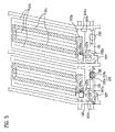
- FIG. 5 is a plan view showing a liquid crystal display device in accordance with a first embodiment of the present invention.
- FIG. 6 is an enlarged plan view showing a first column spacer of FIG. 5 and a peripheral region thereof;
- FIG. 7 is a sectional view showing first and second column spacers of FIG. 5 ;
- FIG. 8 is an enlarged plan view showing a first column spacer and a peripheral region thereof included in a liquid crystal display device in accordance with a second embodiment of the present invention.
- FIG. 9 is a sectional view showing first and second column spacers of the liquid crystal display device in accordance with the second embodiment of the present invention.
- FIGS. 10A to 10E are sectional views showing sequential processes of a method for manufacturing the first and second column spacers of the liquid crystal display device in accordance with an embodiment of the present invention.
- FIG. 4 is a plan view showing the configuration of a protrusion included in the liquid crystal display device in accordance with an embodiment of the present invention.
- the liquid crystal display device using a protrusion includes: first and second substrates 60 and 70 arranged to face each other; at least one column spacer 80 formed on the first substrate 60 at a predetermined position of the first substrate 60 ; a protrusion 85 formed on the second substrate 70 to come into partial contact with the column spacer 80 , the protrusion 85 having a smaller volume than the column spacer 80 ; and a liquid crystal layer (not shown) filled between the first and second substrates 60 and 70 .
- the first and second substrates 60 and 70 are shifted relative to each other.
- the protrusion 85 serves to reduce a frictional force between the column spacer 80 and the second substrate 70 . More specifically, since the protrusion 85 has a smaller area than the column spacer 80 , the contact area is significantly reduced from the larger bottom surface of the column spacer 80 to the smaller area of the protrusion 85 , resulting in a reduced frictional area. As a result, a frictional force between the column spacer 80 and the second substrate 70 is reduced when the first and second substrates 60 and 70 are shifted relative to each other by a touch action. This allows rapid restoration to the original state.
- the column spacer 80 and the pressed single or plural layers below the column spacer 80 can stably maintain a desired cell gap between the first and second substrates 60 and 70 as they restore their original state so long as they are not excessively pressed. This can prevent a gravity defect caused by falling of liquid crystals.
- the protrusion 85 when the protrusion 85 is formed at the center of the column spacer 80 to come into contact with the column spacer 80 , due to the fact that the protrusion 85 has a surface area smaller than that of the column spacer 80 and the column spacer 80 is made of an elastic material softer than that of the protrusion 85 , the column spacer 80 may be excessively pressed by the protrusion 85 at the contact portion thereof.
- liquid crystal display device which are capable of preventing not only a touch defect and a gravity defect, but also plastic deformation of the column spacer and layers arranged below the column spacer through the use of a protrusion, will be explained with reference to the accompanying drawings.
- FIG. 5 is a plan view showing a liquid crystal display device in accordance with a first embodiment of the present invention.
- FIG. 6 is an enlarged plan view showing a first column spacer of FIG. 5 and a peripheral region thereof.
- FIG. 7 is a sectional view showing first and second column spacers of FIG. 5 .
- the liquid crystal display device in accordance with the first embodiment of the present invention includes: a first substrate 100 and a second substrate 200 that are arranged to face each other; and a liquid crystal layer (not shown) filled between the first and second substrates 100 and 200 .
- the first substrate 100 includes: a plurality of gate lines 101 and data lines 102 that intersect each other and adapted to define pixel regions; thin film transistors (TFT) formed at intersections of the gate lines and data lines; first storage electrodes 103 a electrically connected to drain electrodes 102 b of the TFTs, respectively; pixel electrodes 103 branched from the respective first storage electrodes 103 a ; common electrodes 104 branched from respective second storage electrodes, so as to be arranged alternately with the pixel electrodes 103 ; common lines 104 a extending parallel to the gate lines 101 ; and the second storage electrodes 104 b connected to the common lines 104 a and the common electrodes 104 to be overlapped with the respective first storage electrodes 103 a.
- TFT thin film transistors
- Each of the TFTs includes: a source electrode 102 a ; the drain electrode 102 b ; and a channel region defined between the source and drain electrodes 102 a and 102 b .
- the source electrode 102 a has a U-shaped inner contour, and accordingly, the channel region has a U-shaped form.
- the TFT further includes a gate electrode 101 a protruding from one of the gate lines 101 .
- the U-shaped source electrode 102 a protrudes from one of the data lines 102
- the drain electrode 102 b extends into the U-shaped source electrode 102 a while being spaced apart from the source electrode 102 a by a predetermined distance.
- the TFT further includes a semiconductor layer (not shown in FIGS.
- the semiconductor layer has a laminated structure including an amorphous silicon layer (not shown) and an n+ layer (impurity layer) (not shown) formed on the amorphous silicon layer.
- the n+ layer (impurity layer) is removed from a portion of the semiconductor layer corresponding to the channel region between the source and drain electrodes 102 a and 102 b .
- the semiconductor layer may be selectively formed below the source/drain electrodes 102 a and 102 b and below the channel region between the source/drain electrodes 102 a and 102 b , or may be formed below the data line 102 , source electrode 102 a , and drain electrode 102 b other than the channel region.
- the liquid crystal display device in this illustrated embodiment has the U-shaped source electrode 102 a and U-shaped channel region, it will be appreciated that the present invention is applicable even when the source electrode 102 a has a linear or any other shape.
- the gate lines 101 , common lines 104 a , and common electrodes 104 are made of the same metal as each other to form the same layer.
- a gate insulation layer 105 is interposed between the gate lines 101 and the semiconductor layer, and a protective layer 106 is interposed between the data lines 102 and the pixel electrodes 103 .
- each second storage electrode 104 b connected to one of the common lines 104 a that pass through the pixel regions, the first storage electrode 103 a formed on the second storage electrode 104 b , and the gate insulation layer 105 and protective layer 106 interposed between the two electrodes constitute a storage capacitor.
- the drain electrodes 102 b are formed at a different layer from that of the storage electrodes 103 a , such that they come into contact with each other through contact holes 106 a .
- the contact holes 106 a are formed by removing predetermined portions of the protective layer 106 above the respective drain electrodes 102 b.
- a plurality of protrusions 120 are formed at predetermined positions above the gate lines 101 .
- Each of the protrusions 120 has a laminated structure including a semiconductor layer pattern 121 a and a source/drain metal layer pattern 122 a formed on the semiconductor layer pattern 121 a .
- the protrusion 120 is configured such that a closed loop shaped recess is formed in a first pattern 120 a having a rectangular horizontal cross section as shown in FIG. 6 .
- the closed loop may have a circular, polygonal or other shapes.
- a circular or polygonal second pattern 120 b which is smaller than the closed loop shaped recess, is formed inside the recess.
- the circular closed loop shaped recess and the circular second pattern 120 b are shown in FIGS. 5 and 6 , the present invention is not limited thereto. Polygonal or other shapes may be also adopted.
- the first pattern 120 a includes the semiconductor layer pattern 121 a and the source/drain metal layer pattern 122 a
- the second pattern 120 b includes the semiconductor layer (which is in the same layer as the semiconductor layer pattern 121 a ).
- the first pattern 120 a is spaced apart from the second pattern 120 b by a predetermined distance.
- the first pattern 120 a forms the rectangular boundary of the protrusion 120
- the second pattern 120 b is formed at the center of the rectangular first pattern 120 a .
- the protrusion 120 including the first and second patterns 120 a and 120 b , has a gap between the first and second patterns 120 a and 120 b.
- the semiconductor layer pattern 121 a has a thickness of approximately 0.2 to 0.3 ⁇ m
- the source/drain metal layer pattern 122 a has a thickness of approximately 0.2 to 0.4 ⁇ m.
- the first pattern 120 a is raised by a height of approximately 0.4 to 0.7 ⁇ m
- the second pattern 120 b is raised by a height of approximately 0.2 to 0.4 ⁇ m. Accordingly, the first and second patterns 120 a and 120 b have a height difference equal to the thickness of the source/drain metal layer pattern 122 a .
- a space having a W-shaped vertical cross section is formed between the protrusion 120 and a first column spacer 210 corresponding to the protrusion 120 after the first and second substrates 100 and 200 are bonded to each other.
- the protective layer 106 is formed over the protrusion 120 except for the contact hole 106 a . Accordingly, the protective layer 106 on the protrusion 120 may be a portion that actually comes into contact with the first column spacer 210 that is formed on the second substrate 200 . However, in another embodiment, the protective layer 106 does not cover the protrusion 120 , and therefore the first column spacer 210 is in contact with the protrusion 120 .
- the second substrate 200 arranged to face the first substrate 100 , includes: a black matrix layer 201 formed at the regions (corresponding to the gate lines and data lines) other than the pixel regions; color filter layers 202 formed on the second substrate 200 including the black matrix layer 201 ; and an overcoat layer 203 formed on the second substrate 200 including the black matrix layer 201 and color filter layers 202 .
- the overcoat layer 203 is for use in a later flattening process.
- the overcoat layer 203 is formed with the first column spacers 210 at positions corresponding to the respective protrusions 120 .
- the overcoat layer 203 is formed with second column spacers 220 at positions corresponding to the regions of the gate lines 101 where the protrusions 120 are not formed.
- both the first and second column spacers 210 and 220 are formed on the overcoat layer 203
- the present invention is not limited to these embodiment with both the first and second column spacers 210 and 220 .
- simply using the first spacer 210 and the corresponding protrusion 120 would also fall within the scope of the present invention.
- the first and second column spacers 210 and 220 are formed on the overcoat layer 203 to have the same height as each other. However, the first and second column spacers 210 and 220 can also have same heights.
- each of the first column spacers 210 comes into contact with the protective layer 106 at a portion of the protective layer 106 above the first pattern 120 a . In this case, a portion of the protective layer 106 above the second pattern 120 b is spaced apart from the first column spacer 210 .
- each of the second column spacers 220 is spaced apart from the protective layer 106 formed on the first substrate 100 by a distance of approximately 0.4 to 0.7 ⁇ m when viewed in a vertical cross section.
- the first column spacer 210 having elasticity is pushed by the corresponding protrusion 120 .
- the first column spacers 210 is initially deformed from a portion thereof corresponding to the first pattern 120 a in contact with the first column spacer 210 , and is finally deformed at a central portion thereof corresponding to the second pattern 120 b in accordance with an increase in the pressure applied to the substrates 100 and 200 .
- the above described configuration of the protrusion and column spacer of the liquid crystal display device can distribute the pressure of the push test onto the first and second patterns 120 a and 120 b , differently from the conventional configuration wherein a protrusion simply corresponds to the center of a column spacer. This increases a contact area between the protrusion 120 and the first column spacer 210 in proportional to the pressure, thereby alleviating excessive plastic deformation of the first column spacer 210 at the contact portion thereof and maintaining a cell gap between the first and second substrates 100 and 200 during the push test.
- the illustrated liquid crystal display device is subjected to a push test wherein a predetermined pressure (beyond a pressure required for bonding two substrates) is applied to the bonded substrates, the contact area between the protrusion 120 and the first column spacer 210 gradually increases. Therefore, as the applied pressure increases, the pressure can be distributed over the surface area of the first column spacer 210 corresponding to the protrusion 120 , rather than being concentrated on a specific portion of the first column spacer 210 . This prevents excessive deformation of the first column spacer 210 at the specific location thereof.
- a predetermined pressure be applied to the bonded substrates
- the second column spacer 220 as well as a portion location of the first column spacer 210 corresponding to the closed loop shaped recess of the protrusion 120 come into contact with the protective layer 106 formed on the first substrate 100 . Therefore, the contact area increases greatly to effective prevent the undesired or excessive deformation of the first and second column spacers 210 and 220 .
- the first column spacer 210 functions as a gap maintenance spacer for maintaining a cell gap between the first and second substrates 100 and 200 .
- the second column spacer 220 functions as a depression prevention spacer for attenuating the deformation of the column spacer when it is pushed.
- the protrusion 120 functions as an auxiliary depression prevention spacer due to the closed loop shaped recess or second pattern 120 b thereof.
- the first pattern 120 a which forms the boundary of the protrusion 120 , comes into contact with the first column spacer 210 . Therefore, the first column spacer 210 is depressed by a certain thickness upon receiving the pressure applied during the bonding process. As a result, a stress is concentrated at the contact region between the first pattern 120 a and the first column spacer 210 . However, since the first column spacer 210 has an elastic restoration force at the stress concentrated portion when liquid crystals are expanded at a high temperature, it can stably maintain a cell gap between the first and second substrates 100 and 200 to some extent.
- the first column spacer 210 elastically overcome a depression force applied thereto by the first pattern 120 a of the protrusion 120 , thereby achieving a supporting force required to maintain the cell gap. Accordingly, the first column spacer provides a desired supporting force even if the liquid crystals are expanded due to a high temperature, thereby preventing a gravity defect.
- positions of the first and second column spacers 210 and 220 are not limited to the gate lines 101 , and may be formed on the common lines 104 a that are the same metal layer as the gate lines 101 .
- each protrusion 120 is positioned to correspond to the relevant first column spacer 210 .
- the protrusions 120 may be formed on the gate lines 101 to correspond to the first column spacers 210 .
- the protrusions 120 may be formed on the common lines 104 a.
- the first and second column spacers 210 and 220 can be formed above the gate lines 101 or common lines 104 a .
- the overcoat layer 203 is laminated on the color filter layer 202
- the color filter layer 202 is laminated on the black matrix layer 201
- the black matrix layer 201 is laminated on the second substrate 200 .
- the protrusions 120 are formed as the thin film transistors, more particularly, the semiconductor layer (designated as reference numeral 107 a of FIG. 10E ) and data line layer including the data lines 102 and source/drain electrodes 102 a and 102 b , are patterned by use of a half-torn mask or diffraction exposure mask.
- FIG. 8 is an enlarged plan view showing a first column spacer and a peripheral region thereof included in a liquid crystal display device in accordance with a second embodiment of the present invention.
- FIG. 9 is a sectional view showing first and second column spacers of the liquid crystal display device in accordance with the second embodiment of the present invention.
- the liquid crystal display device in accordance with the second embodiment of the present invention is basically similar to that of the previously described first embodiment as shown in FIGS. 5 to 7 except for the shape of a protrusion 140 , and the detailed description of the similar configuration will be omitted.
- the protrusion 140 has a laminated structure including a lower semiconductor layer 123 having a rectangular horizontal cross section and an upper source/drain metal layer pattern 124 a having a smaller horizontal cross section than that of the semiconductor layer 123 , a central portion of the source/drain metal layer pattern 124 a being circularly removed.
- a first column spacer 310 is formed to correspond to the protrusion 140 . Both the protrusion 140 and the first column spacer 310 may be formed on the common line 104 a . Also, a second column spacer 320 is formed on the overcoat layer 203 at a position corresponding to a region of the gate line 101 or common line 104 a where the protrusion 140 is not formed.
- the protective layer 106 is formed over the entire surface of the gate insulation layer 105 and over a top of the protrusion 140 .
- the first column spacer 310 is formed on the second substrate 200 to correspond to the protrusion 140 .
- a portion of the protective layer 106 above the source/drain metal layer pattern 124 a comes into contact with the first column spacer 310 .
- a portion of the protective layer 106 which corresponds to the center of the protrusion 140 where the source/drain metal layer pattern 124 a is not formed, is spaced apart from the first column spacer 310 .
- liquid crystal display device in accordance with the second embodiment of the present invention is subjected to a push test wherein a predetermined pressure, which is larger than a pressure applied to bond two substrates, is applied, a portion of the protective layer 106 above the source/drain metal layer pattern 124 a is first pushed by the first column spacer 310 . Finally, a portion of the protective layer 106 , which corresponds to the semiconductor layer 123 of the protrusion 140 where the source/drain metal layer pattern 124 a is not formed, is pushed by the first column spacer 310 .
- a contact area between the protrusion 140 and the first column spacer 310 increases in accordance with an increase in the pressure applied, resulting in distribution of the pressure. This preventing generating a imprinting spot (push spot) at the first column spacer 310 even if an excessively high pressure is applied during the push test.
- FIGS. 10A to 10E are sectional views showing sequential processes of a method for manufacturing the first and second column spacers of the liquid crystal display device in accordance with an embodiment of the present invention(the plan view of the liquid crystal display device refers to FIGS. 5 and 6 ).
- a metal material is deposited over the entire surface of the first substrate 100 .
- the metal material is then selectively removed to form the gate lines 101 arranged in one direction, the common lines 104 a arranged in a direction parallel to the gate lines 101 while being uniformly spaced apart from the gate lines 101 , and the common electrodes 104 branched from the respective common lines 104 a .
- the gate electrodes 101 a protrude from certain portions of the respective gate lines 101 .
- the gate insulation layer 105 is formed over the entire surface of the first substrate 100 including the gate electrodes 101 a , gate lines 101 , common lines 104 a , and common electrodes 104 .
- the semiconductor layer 107 and the metal layer 112 are deposited in sequence over the entire surface of the first substrate 100 including the gate insulation layer 105 .
- the semiconductor layer 107 has a laminated structure including an amorphous silicon layer and an impurity layer formed on the amorphous silicon layer.
- a mask 400 which is defined with light shielding portions 401 , semi-transparent portions 403 , and transparent portions 402 , is prepared.
- the mask 400 is aligned on a top of the first substrate 100 including the coated photosensitive layer 130 .
- the light shielding portions 401 of the mask 400 correspond to the regions where the metal layer 112 and semiconductor layer 107 will be completely removed after a patterning process
- the transparent portions 402 correspond to the regions where the metal layer 112 and semiconductor layer 107 will remain after the patterning process
- the semi-transparent portions 403 correspond to the regions where only the semiconductor layer 107 will remain after the patterning process.
- the photosensitive layer 130 is then primarily exposed and developed by use of the mask 400 , to form a first photosensitive layer pattern 130 a.
- the regions of the first photosensitive layer pattern 130 a corresponding to the transparent portions 402 and the semi-transparent portions 403 of the mask 400 remain. Specifically, the regions of the first photosensitive layer pattern 130 a corresponding to the semi-transparent portions 403 are further removed to have a thickness thinner than that of the remaining regions of the first photosensitive layer pattern 130 a corresponding to the transparent portions 402 . As a result, the first photosensitive layer pattern 130 a has a stepped structure rather than a flat structure.
- the metal layer 112 is patterned by use of the first photosensitive layer pattern 130 a and an etching solution or gas that is capable of selectively etching the metal layer 112 , to form a metal layer pattern 112 a (see FIG. 10C ).
- the semiconductor layer 107 is etched by use of the first photosensitive layer pattern 130 a and an etching solution or gas that is capable of selectively etching the semiconductor layer 107 , to form the semiconductor layer 107 a of each thin film transistor (TFT), and to form the semiconductor layer pattern 121 a of the first pattern 120 a and the semiconductor layer pattern 120 b of each protrusion 120 .
- the semiconductor layer pattern 121 a of the first pattern 120 a is a portion corresponding to an outer periphery of the protrusion 120
- the semiconductor layer pattern 120 b is a portion corresponding to the center of the protrusion 120 .
- an ashing process is performed to completely remove the thinner portion of the stepped first photosensitive layer pattern 130 a , to form a second photosensitive layer pattern 130 b.
- the source/drain electrodes 102 a and 102 b and the source/drain metal layer pattern 122 a that constitute the first pattern 120 a of each protrusion 120 are formed by use of the second photosensitive layer pattern 130 b and an etching solution or gas that is capable of selectively etching a metal layer.
- the impurity layer in the channel region is removed by using the source/drain metal layer pattern 122 a as an etching mask and by use of an etching solution or gas that is capable of selectively removing the impurity layer.
- the data lines 102 are further patterned to extend in a direction perpendicular to the gate lines 101 .
- the source electrodes 102 a are formed to protrude from the data lines 102 .
- the protective layer 106 is formed over the entire surface of the first substrate 100 including the semiconductor layer 107 a , source/drain electrodes 102 a and 102 b , and protrusion 120 .
- the shapes of the transparent portion and light shielding portion of the mask 400 are determined depending on whether the photosensitive layer has a negative photosensitivity or positive photosensitivity.
- the accompanying drawings illustrate the case wherein the photosensitive layer 130 has a negative photosensitivity. If the photosensitive layer 130 has a positive photosensitivity, the shapes of the transparent portion and light shielding portion of the mask 400 are reversed, but the same patterning effect can be achieved in both the cases.
- the protective layer 106 is selectively removed at positions above the respective drain electrodes 102 b , to form the contact holes 106 a.
- a transparent electrode material is deposited over the entire surface of the protective layer 106 including the contact holes 106 a .
- the transparent electrode material is then selectively removed, to form the pixel electrodes 103 arranged alternately with the common electrodes 104 .
- the black matrix layer 201 is formed on the second substrate 200 at portions corresponding to the regions other than the pixel regions, and the color filter layer 202 is formed on the black matrix layer 201 at portions corresponding to the pixel regions.
- the overcoat layer 203 is formed over the entire surface of the second substrate 200 including the black matrix layer 201 and color filter layer 202 .
- a liquid crystal material (not shown) is deposited onto the first substrate 100 or second substrate 200 , and the remaining substrate 200 or 100 , on which no liquid crystal material is deposited, is turned over, to bond the first and second substrates 100 and 200 each other.
- the above embodiments of the present invention takes an in-plane switching (IPS) mode as an example, but the present invention is also applicable to a twist nematic (TN) mode.
- the twist nematic mode is similar to the above described IPS mode except for that a pixel electrode on each pixel region of a first substrate has a single pattern, and a common electrode is formed over the entire surface of a second substrate. In the case of the twist nematic mode, no common line is formed at the pixel regions, and therefore, all of first and second column spacers and protrusion are formed on gate lines.
- liquid crystal display device As apparent from the above description, the liquid crystal display device and the method for manufacturing the same have advantages as follows:
- a protrusion may be configured to correspond to the entire column spacer and may have a stepped structure due to a recess formed therein. With this configuration, only an outer periphery of the protrusion comes into contact with the column spacer when first and second substrates are bonded to each other. This reduces a contact area between the first and second substrates (more particularly, a contact area between the protrusion and the column spacer), thereby allowing rapid restoration to the original state even if a touch occurs, as compared to a conventional column spacer that wholly comes into contact with a substrate. As a result, the risk of a touch defect is significantly reduced.
- the column spacer when the illustrated liquid crystal display device is subjected to a push test wherein a pressure, which is higher than a pressure applied for the bonding of both the substrates, is applied, the column spacer, which initially comes into contact with only the outer periphery of the protrusion when the substrates are bonded to each other, provides a gradually increased contact area to the protrusion due to the stepped structure of the protrusion. Specifically, as the pressure applied during the push test increases, the column spacer gradually comes into contact with the protrusion from a relatively shallow portion to a relatively deep portion of the recess formed in the protrusion. This can distribute the applied pressure upon the push test. As a result, the plastic deformation at the column spacer where the pressure is concentrated is alleviated, resulting in prevention of a imprinting spot.
- the portion of the column spacer which is depressed by the outer periphery of the protrusion upon bonding of the substrates, acts to compensate for the expansion of the liquid crystals, thereby achieving a predetermined gravity margin, and preventing a gravity defect to some extent.
Abstract
Description
Claims (39)
Applications Claiming Priority (2)
| Application Number | Priority Date | Filing Date | Title |
|---|---|---|---|
| KR10-2005-0090657 | 2005-09-28 | ||
| KR1020050090657A KR101157954B1 (en) | 2005-09-28 | 2005-09-28 | Liquid Crystal Display Device and Method for Manufacturing the Same |
Publications (2)
| Publication Number | Publication Date |
|---|---|
| US20070070286A1 US20070070286A1 (en) | 2007-03-29 |
| US7518695B2 true US7518695B2 (en) | 2009-04-14 |
Family
ID=36888344
Family Applications (1)
| Application Number | Title | Priority Date | Filing Date |
|---|---|---|---|
| US11/477,520 Active 2027-05-29 US7518695B2 (en) | 2005-09-28 | 2006-06-30 | Liquid crystal display device, method for manufacturing the same and spacer structure |
Country Status (8)
| Country | Link |
|---|---|
| US (1) | US7518695B2 (en) |
| JP (1) | JP4578443B2 (en) |
| KR (1) | KR101157954B1 (en) |
| CN (1) | CN100507658C (en) |
| DE (1) | DE102006028993B4 (en) |
| FR (1) | FR2891376B1 (en) |
| GB (1) | GB2430758B (en) |
| TW (1) | TWI342968B (en) |
Cited By (2)
| Publication number | Priority date | Publication date | Assignee | Title |
|---|---|---|---|---|
| US20080212006A1 (en) * | 2007-03-01 | 2008-09-04 | Seiko Epson Corporation | Liquid crystal device and electronic apparatus |
| US20130342781A1 (en) * | 2012-06-25 | 2013-12-26 | Lg Display Co., Ltd. | Liquid crystal display device and method for fabricating the same |
Families Citing this family (27)
| Publication number | Priority date | Publication date | Assignee | Title |
|---|---|---|---|---|
| KR101137842B1 (en) * | 2005-09-23 | 2012-04-20 | 엘지디스플레이 주식회사 | Liquid Crystal Display Device and Method for Manufacturing the Same |
| KR100840095B1 (en) * | 2007-01-22 | 2008-06-19 | 삼성에스디아이 주식회사 | Liquid crystal display device and fabrication method thereof |
| KR101363746B1 (en) * | 2007-04-10 | 2014-02-21 | 엘지디스플레이 주식회사 | liquid crystal display and method of manufacturing the same |
| US8330887B2 (en) * | 2007-07-27 | 2012-12-11 | Semiconductor Energy Laboratory Co., Ltd. | Liquid crystal display device and electronic device |
| JP5323329B2 (en) * | 2007-08-10 | 2013-10-23 | パナソニック液晶ディスプレイ株式会社 | Liquid crystal display |
| KR20090100639A (en) * | 2008-03-20 | 2009-09-24 | 삼성전자주식회사 | Display panel and manufacturing method of the same |
| JP5318498B2 (en) * | 2008-08-26 | 2013-10-16 | 株式会社ジャパンディスプレイ | Liquid crystal display |
| TWI384273B (en) * | 2008-10-31 | 2013-02-01 | Au Optronics Corp | Touch display panel |
| CN101770100B (en) * | 2008-12-31 | 2011-12-28 | 上海天马微电子有限公司 | Touch liquid crystal display device and touch recognition method |
| JP2010237503A (en) * | 2009-03-31 | 2010-10-21 | Hitachi Displays Ltd | Liquid crystal display |
| JP5580657B2 (en) * | 2010-04-27 | 2014-08-27 | 三菱電機株式会社 | Liquid crystal display |
| KR101717651B1 (en) * | 2010-10-14 | 2017-03-20 | 엘지디스플레이 주식회사 | Liquid crystal display device and method for fabricating the same |
| DK2746824T3 (en) * | 2011-09-15 | 2017-02-13 | Soken Kagaku Kk | Contact preventive film, touch panel and cover plate for a screen device |
| CN102707356B (en) * | 2011-11-01 | 2014-05-21 | 京东方科技集团股份有限公司 | Method for manufacturing color filter, color filter and display device |
| JP5917126B2 (en) | 2011-12-19 | 2016-05-11 | 株式会社ジャパンディスプレイ | Liquid crystal display |
| CN102591048A (en) * | 2012-03-26 | 2012-07-18 | 深圳市华星光电技术有限公司 | Liquid crystal display panel, manufacturing method for same and liquid crystal display device |
| CN102736311B (en) | 2012-06-15 | 2015-05-20 | 深圳市华星光电技术有限公司 | Liquid crystal display panel and method for manufacturing same |
| CN103869560A (en) * | 2012-12-14 | 2014-06-18 | 瀚宇彩晶股份有限公司 | Pixel structure of liquid crystal display panel and pixel forming method |
| JP2013054391A (en) * | 2012-12-18 | 2013-03-21 | Japan Display East Co Ltd | Liquid crystal display device |
| CN104238197B (en) * | 2014-07-24 | 2017-06-16 | 合肥鑫晟光电科技有限公司 | A kind of chock insulator matter, display panel and display device |
| KR101712246B1 (en) * | 2014-12-05 | 2017-03-06 | 엘지디스플레이 주식회사 | Self-capacitive touch sensor integrated type display device |
| CN104900709B (en) * | 2015-06-04 | 2017-11-17 | 福州大学 | A kind of high-performance bottom gate type TFT device architectures and preparation method thereof |
| KR102316560B1 (en) * | 2015-07-29 | 2021-10-25 | 엘지디스플레이 주식회사 | Substrate including thin film transistor and display panel having the smae |
| US20200004073A1 (en) * | 2017-03-15 | 2020-01-02 | Sharp Kabushiki Kaisha | Liquid crystal display device |
| CN107402478B (en) * | 2017-08-17 | 2021-01-08 | 惠科股份有限公司 | Display device, display panel and manufacturing method thereof |
| CN111045260A (en) * | 2019-12-12 | 2020-04-21 | Tcl华星光电技术有限公司 | Pressure-resistant liquid crystal display structure and manufacturing method thereof |
| KR20220025987A (en) * | 2020-08-24 | 2022-03-04 | 삼성디스플레이 주식회사 | Display device |
Citations (11)
| Publication number | Priority date | Publication date | Assignee | Title |
|---|---|---|---|---|
| JPH03197928A (en) | 1989-12-27 | 1991-08-29 | Citizen Watch Co Ltd | Liquid crystal display device |
| US6157431A (en) * | 1997-03-11 | 2000-12-05 | Sharp Kabushiki Kaisha | Liquid crystal display apparatus suppressed of orientation defect having metal film and photosensitive resin as a columnar spacer and fabrication method thereof |
| US6411360B1 (en) * | 1999-06-18 | 2002-06-25 | Hitachi, Ltd. | Inplane switching type liquid crystal display with alignment layer formed on columnar spacer directly |
| US20050088606A1 (en) * | 2003-10-27 | 2005-04-28 | Hitachi Displays, Ltd. | Liquid crystal display device |
| CN1661425A (en) | 2004-02-25 | 2005-08-31 | Lg.菲利浦Lcd株式会社 | Liquid crystal display device and method of fabricating the same |
| US20050243263A1 (en) * | 2004-04-30 | 2005-11-03 | Lg.Philips Lcd Co., Ltd. | Liquid crystal display device and method for fabricating the same |
| US7133108B2 (en) * | 2000-12-08 | 2006-11-07 | Hitachi, Ltd. | Liquid crystal display device |
| US20060290860A1 (en) * | 2005-06-28 | 2006-12-28 | Lg Philips Lcd Co., Ltd. | Liquid crystal display device |
| US20070002237A1 (en) * | 2005-06-30 | 2007-01-04 | Yoon Sung H | Liquid crystal display device and method for manufacturing the same |
| US20070132936A1 (en) * | 2005-12-13 | 2007-06-14 | Lg.Philips Lcd Co., Ltd. | Liquid crystal display device and method of fabricating the same |
| US20070139604A1 (en) * | 2005-12-15 | 2007-06-21 | Lg.Philips Lcd Co., Ltd. | Liquid crystal display device and method for manufacturing the same |
Family Cites Families (7)
| Publication number | Priority date | Publication date | Assignee | Title |
|---|---|---|---|---|
| JPH11153798A (en) * | 1997-11-20 | 1999-06-08 | Toshiba Corp | Active matrix type liquid crystal display device |
| KR20040012309A (en) * | 2002-08-02 | 2004-02-11 | 엘지.필립스 엘시디 주식회사 | liquid crystal panel including patterned spacer |
| KR100894044B1 (en) * | 2003-01-30 | 2009-04-20 | 삼성전자주식회사 | Liquid crystal display |
| KR100489282B1 (en) * | 2003-06-17 | 2005-05-17 | 엘지.필립스 엘시디 주식회사 | Thin Film Transistor Array Substrate And Fabricating Method Thereof |
| TWI247959B (en) * | 2004-01-30 | 2006-01-21 | Chi Mei Optoelectronics Corp | Liquid crystal display device |
| KR100672651B1 (en) * | 2004-02-25 | 2007-01-24 | 엘지.필립스 엘시디 주식회사 | Liquid Crystal Display Device and method for manufacturing the same |
| KR100617039B1 (en) * | 2004-02-26 | 2006-08-30 | 엘지.필립스 엘시디 주식회사 | Liquid Crystal Display Device and method for Manufacturing the same |
-
2005
- 2005-09-28 KR KR1020050090657A patent/KR101157954B1/en active IP Right Grant
-
2006
- 2006-06-19 JP JP2006169085A patent/JP4578443B2/en not_active Expired - Fee Related
- 2006-06-23 DE DE102006028993.5A patent/DE102006028993B4/en not_active Expired - Fee Related
- 2006-06-27 FR FR0605755A patent/FR2891376B1/en not_active Expired - Fee Related
- 2006-06-28 CN CNB2006100942713A patent/CN100507658C/en active Active
- 2006-06-28 TW TW095123421A patent/TWI342968B/en not_active IP Right Cessation
- 2006-06-29 GB GB0612962A patent/GB2430758B/en not_active Expired - Fee Related
- 2006-06-30 US US11/477,520 patent/US7518695B2/en active Active
Patent Citations (12)
| Publication number | Priority date | Publication date | Assignee | Title |
|---|---|---|---|---|
| JPH03197928A (en) | 1989-12-27 | 1991-08-29 | Citizen Watch Co Ltd | Liquid crystal display device |
| US6157431A (en) * | 1997-03-11 | 2000-12-05 | Sharp Kabushiki Kaisha | Liquid crystal display apparatus suppressed of orientation defect having metal film and photosensitive resin as a columnar spacer and fabrication method thereof |
| US6411360B1 (en) * | 1999-06-18 | 2002-06-25 | Hitachi, Ltd. | Inplane switching type liquid crystal display with alignment layer formed on columnar spacer directly |
| US7133108B2 (en) * | 2000-12-08 | 2006-11-07 | Hitachi, Ltd. | Liquid crystal display device |
| US20050088606A1 (en) * | 2003-10-27 | 2005-04-28 | Hitachi Displays, Ltd. | Liquid crystal display device |
| CN1661425A (en) | 2004-02-25 | 2005-08-31 | Lg.菲利浦Lcd株式会社 | Liquid crystal display device and method of fabricating the same |
| GB2411485A (en) | 2004-02-25 | 2005-08-31 | Lg Philips Lcd Co Ltd | Liquid crystal display device and method of fabricating the same |
| US20050243263A1 (en) * | 2004-04-30 | 2005-11-03 | Lg.Philips Lcd Co., Ltd. | Liquid crystal display device and method for fabricating the same |
| US20060290860A1 (en) * | 2005-06-28 | 2006-12-28 | Lg Philips Lcd Co., Ltd. | Liquid crystal display device |
| US20070002237A1 (en) * | 2005-06-30 | 2007-01-04 | Yoon Sung H | Liquid crystal display device and method for manufacturing the same |
| US20070132936A1 (en) * | 2005-12-13 | 2007-06-14 | Lg.Philips Lcd Co., Ltd. | Liquid crystal display device and method of fabricating the same |
| US20070139604A1 (en) * | 2005-12-15 | 2007-06-21 | Lg.Philips Lcd Co., Ltd. | Liquid crystal display device and method for manufacturing the same |
Cited By (5)
| Publication number | Priority date | Publication date | Assignee | Title |
|---|---|---|---|---|
| US20080212006A1 (en) * | 2007-03-01 | 2008-09-04 | Seiko Epson Corporation | Liquid crystal device and electronic apparatus |
| US8004642B2 (en) * | 2007-03-01 | 2011-08-23 | Seiko Epson Corporation | Liquid crystal display device comprising transition electrodes having a same potential as a corresponding one of the scanning lines |
| US20110228206A1 (en) * | 2007-03-01 | 2011-09-22 | Seiko Epson Corporation | Liquid crystal device and electronic apparatus |
| US20130342781A1 (en) * | 2012-06-25 | 2013-12-26 | Lg Display Co., Ltd. | Liquid crystal display device and method for fabricating the same |
| US9335600B2 (en) * | 2012-06-25 | 2016-05-10 | Lg Display Co., Ltd. | Liquid crystal display device and method for fabricating the same |
Also Published As
| Publication number | Publication date |
|---|---|
| KR20070035820A (en) | 2007-04-02 |
| JP2007094372A (en) | 2007-04-12 |
| FR2891376B1 (en) | 2011-10-28 |
| JP4578443B2 (en) | 2010-11-10 |
| TWI342968B (en) | 2011-06-01 |
| CN1940659A (en) | 2007-04-04 |
| DE102006028993B4 (en) | 2014-02-13 |
| GB2430758B (en) | 2007-12-05 |
| CN100507658C (en) | 2009-07-01 |
| GB2430758A (en) | 2007-04-04 |
| DE102006028993A1 (en) | 2007-04-19 |
| US20070070286A1 (en) | 2007-03-29 |
| FR2891376A1 (en) | 2007-03-30 |
| GB0612962D0 (en) | 2006-08-09 |
| KR101157954B1 (en) | 2012-06-22 |
| TW200712631A (en) | 2007-04-01 |
Similar Documents
| Publication | Publication Date | Title |
|---|---|---|
| US7518695B2 (en) | Liquid crystal display device, method for manufacturing the same and spacer structure | |
| US7684002B2 (en) | Liquid crystal display device and fabricating the same | |
| JP3768367B2 (en) | Liquid crystal display | |
| US7684003B2 (en) | Liquid crystal display device and method for manufacturing the same | |
| US7826026B2 (en) | Liquid crystal display device and method for fabricating the same | |
| JP4566951B2 (en) | Liquid crystal display device and manufacturing method thereof | |
| JP4532231B2 (en) | Liquid crystal display device and manufacturing method thereof | |
| KR101182314B1 (en) | Liquid Crystal Display Device and Method for Manufacturing the Same | |
| US20060226426A1 (en) | Liquid crystal display device | |
| JP2005242310A (en) | Liquid crystal display device and method of fabricating same | |
| KR101717651B1 (en) | Liquid crystal display device and method for fabricating the same | |
| KR101192761B1 (en) | Liquid Crystal Display Device and method of manufacturing the same | |
| US8120733B2 (en) | Liquid crystal display device and method for manufacturing the same | |
| US7525622B2 (en) | Liquid crystal display device and method for fabricating the same | |
| JP2010054552A (en) | Liquid crystal display device | |
| KR101244663B1 (en) | Method for Manufacturing the Same | |
| KR20080079141A (en) | Liquid crystal display device having dual column spacers and method of fabricating thereof | |
| US20040156007A1 (en) | Substrate for liquid crystal display and liquid crystal display having the same | |
| JP2011141466A (en) | Method of manufacturing microlens substrate, method of manufacturing electrooptical device, and electrooptical device |
Legal Events
| Date | Code | Title | Description |
|---|---|---|---|
| AS | Assignment |
Owner name: LG. PHILIPS LCD CO., LTD., KOREA, REPUBLIC OF Free format text: ASSIGNMENT OF ASSIGNORS INTEREST;ASSIGNORS:CHO, SUK HO;YUN, JE PIL;REEL/FRAME:018030/0491;SIGNING DATES FROM 20060629 TO 20060630 |
|
| AS | Assignment |
Owner name: LG DISPLAY CO., LTD., KOREA, REPUBLIC OF Free format text: CHANGE OF NAME;ASSIGNOR:LG.PHILIPS LCD CO., LTD.;REEL/FRAME:020985/0675 Effective date: 20080304 Owner name: LG DISPLAY CO., LTD.,KOREA, REPUBLIC OF Free format text: CHANGE OF NAME;ASSIGNOR:LG.PHILIPS LCD CO., LTD.;REEL/FRAME:020985/0675 Effective date: 20080304 |
|
| FEPP | Fee payment procedure |
Free format text: PAYOR NUMBER ASSIGNED (ORIGINAL EVENT CODE: ASPN); ENTITY STATUS OF PATENT OWNER: LARGE ENTITY |
|
| STCF | Information on status: patent grant |
Free format text: PATENTED CASE |
|
| FEPP | Fee payment procedure |
Free format text: PAYOR NUMBER ASSIGNED (ORIGINAL EVENT CODE: ASPN); ENTITY STATUS OF PATENT OWNER: LARGE ENTITY Free format text: PAYER NUMBER DE-ASSIGNED (ORIGINAL EVENT CODE: RMPN); ENTITY STATUS OF PATENT OWNER: LARGE ENTITY |
|
| FPAY | Fee payment |
Year of fee payment: 4 |
|
| FPAY | Fee payment |
Year of fee payment: 8 |
|
| MAFP | Maintenance fee payment |
Free format text: PAYMENT OF MAINTENANCE FEE, 12TH YEAR, LARGE ENTITY (ORIGINAL EVENT CODE: M1553); ENTITY STATUS OF PATENT OWNER: LARGE ENTITY Year of fee payment: 12 |