US9495494B2 - Circuit simulating method, circuit simulating apparatus, and method of manufacturing semiconductor device - Google Patents
Circuit simulating method, circuit simulating apparatus, and method of manufacturing semiconductor device Download PDFInfo
- Publication number
- US9495494B2 US9495494B2 US14/645,309 US201514645309A US9495494B2 US 9495494 B2 US9495494 B2 US 9495494B2 US 201514645309 A US201514645309 A US 201514645309A US 9495494 B2 US9495494 B2 US 9495494B2
- Authority
- US
- United States
- Prior art keywords
- circuit
- value
- intermediate parameter
- electrical
- parameter value
- Prior art date
- Legal status (The legal status is an assumption and is not a legal conclusion. Google has not performed a legal analysis and makes no representation as to the accuracy of the status listed.)
- Expired - Fee Related, expires
Links
Images


Classifications
-
- G06F17/5036—
-
- G—PHYSICS
- G06—COMPUTING OR CALCULATING; COUNTING
- G06F—ELECTRIC DIGITAL DATA PROCESSING
- G06F30/00—Computer-aided design [CAD]
- G06F30/30—Circuit design
- G06F30/36—Circuit design at the analogue level
- G06F30/367—Design verification, e.g. using simulation, simulation program with integrated circuit emphasis [SPICE], direct methods or relaxation methods
-
- G06F17/5045—
-
- G—PHYSICS
- G06—COMPUTING OR CALCULATING; COUNTING
- G06F—ELECTRIC DIGITAL DATA PROCESSING
- G06F30/00—Computer-aided design [CAD]
- G06F30/30—Circuit design
Definitions
- Embodiments described herein relate generally to a circuit simulating method, a circuit simulating apparatus, and a method of manufacturing a semiconductor device.
- a circuit that meets a required specification is designed using a circuit simulator by digitizing connection information about the circuit and checking whether or not the resulting data meets the required specification.
- a circuit element forming the actual circuit varies in characteristics with time during operation, unlike an ideal model of the circuit element obtained by simulation.
- Such a circuit element having variable characteristics can disable, or cause malfunction of, a system that incorporates the circuit element.
- circuit simulators incorporate a tool that modifies a circuit element model to allow for the aging degradation of the characteristics of the circuit element.
- circuit simulators have a problem that they cannot always design a circuit that reflects the aging degradation of the electrical characteristics of the actual circuit element.
- FIG. 1 is a block diagram showing a circuit simulating apparatus 1 according to an embodiment
- FIG. 2 is a flow chart showing an example of an operation of the circuit simulating apparatus shown in FIG. 1 ;
- FIG. 3A is a diagram showing an equivalent circuit model of a MOS transistor before degradation of a threshold voltage.
- FIG. 3B is a diagram showing an equivalent circuit model of the MOS transistor after degradation of the threshold voltage.
- FIG. 4 shows time charts for illustrating an example of an operation of the circuit simulating apparatus shown in FIG. 1 .
- a circuit simulating method includes obtaining a first electrical characteristic value of a circuit element that operates under a predetermined operational condition.
- the circuit simulating method includes correcting the first electrical characteristic value based on a period in which an electrical stress equal to or higher than a reference value is turned off during operation of the circuit element.
- the aging degradation of electrical characteristics may decrease (that is, the electrical characteristics tends to recover) when an electrical stress to a circuit element is turned off, and has invented a circuit simulating method, a circuit simulating apparatus and a method of manufacturing a semiconductor device such as those according to this embodiment.
- Such circuit characteristics that decrease the aging degradation of the electrical characteristics when an electrical stress is turned off is referred to as recovery characteristics.
- recovery characteristics For example, with an MOS transistor, the aging degradation of a threshold voltage decreases with time in a period in which a voltage stress, such as a drain-source voltage or a gate-source voltage, is turned off.
- FIG. 1 is a block diagram showing a circuit simulating apparatus 1 according to the embodiment.
- the circuit simulating apparatus 1 includes a storage device 11 , an input device 12 , a computing device 13 , and an output device 14 .
- the storage device 11 is an example of a computer-readable recording medium according to the embodiment.
- the storage device 11 stores a circuit simulating program.
- the circuit simulating program is a program that makes a computer perform the procedures (A) and (B) described below.
- the intermediate parameter value is a parameter correlated with the aging degradation that increases with time during the period in which the electrical stress equal to or higher than the reference value is applied to the circuit element.
- the intermediate parameter value in the first procedure is set so as to decrease with time during the period in which the electrical stress is turned off.
- the intermediate parameter value is an example of a first electrical characteristic value.
- the first electrical characteristic value is not limited to the intermediate parameter value and may be any electrical characteristic value that indicates the recovery characteristics.
- the first procedure is an example of a procedure of obtaining the first electrical characteristic value when the circuit element whose electrical characteristics vary with time is operating under a predetermined operational condition.
- the second procedure is an example of a procedure of correcting the first electrical characteristic value based on the period in which the electrical stress equal to or higher than the reference value is turned off during operation of the circuit element.
- the circuit element is not particularly limited and may be any circuit element that has characteristics that the aging degradation of the electrical characteristics decreases when the electrical stress equal to or higher than the reference value is turned off, that is, the recovery characteristics.
- a preferred example of the circuit element is an MOS transistor.
- a more preferred example of the circuit element is a double-diffused MOS (DMOS) transistor.
- the DMOS transistor is designed to handle a large current and has proved that the aging degradation of the electrical characteristics of the DMOS transistor due to the recovery characteristics is larger than that of other MOS transistors. Therefore, the circuit simulation that takes the recovery characteristics into consideration is more effective for the DMOS transistor.
- the electrical stress is a voltage stress or a current stress, for example.
- the electrical stress equal to or higher than the reference value is an electrical stress equal to or higher than a value that is considered to cause degradation of the electrical characteristics of the circuit element, for example.
- the reference value may be any value that is higher than the value at the time when no electrical stress is applied (that is, zero).
- the reference value may be a threshold voltage when the electrical stress is the gate-source voltage of an MOS transistor. In that case, turning off the electrical stress equal to or higher than the reference value is equivalent to turning off the MOS transistor.
- the aging degradation of the electrical characteristics of the circuit element is the aging degradation ⁇ Vth of a threshold voltage of the MOS transistor, the aging degradation ⁇ Idr of a current driving capacity of the MOS transistor, or the aging degradation ⁇ Ron of an on-resistance of the MOS transistor, for example.
- the operational condition of the circuit element is the value of a voltage stress, the value of a current stress, the temperature of the circuit element, or the size of the circuit element, for example.
- the intermediate parameter value is a parameter from which the aging degradation of the electrical characteristics of the circuit element, that is, a target parameter, can be calculated.
- the intermediate parameter value in this embodiment differs from the normal intermediate parameter value and is a parameter that takes into consideration the recovery characteristics of the circuit element. The intermediate parameter value will be described in further detail later.
- the storage device 11 stores not only the circuit simulating program described above but also a circuit simulator that performs a normal circuit simulation based on a net list in a computer-readable manner.
- the circuit simulating program is incorporated in a circuit simulator as a tool of the circuit simulator, for example.
- the storage device 11 further stores a circuit diagram editor used for input of a net list in a computer-readable manner.
- the input device 12 creates a net list using the circuit diagram editor read from the storage device 11 and inputs the created net list to the computing device 13 .
- the net list contains not only information required for execution of the normal circuit simulation, such as connection information about circuit elements, but also aging information used to specify the characteristics of the circuit element of which future year is to be analyzed.
- the input device 12 can be implemented by various types of input user interfaces, computers and displays, for example.
- the computing device 13 executes the circuit simulating program read from the storage device 11 to operate as a first calculating part and a second calculating part. That is, the computing device 13 performs the first procedure (A) and the second procedure (B) described above.
- the computing device 13 outputs to the output device 14 the aging degradation of the electrical characteristics calculated in the second procedure.
- the computing device 13 can be implemented by a computer.
- the computing device 13 may share common hardware with the input device 12 .
- the output device 14 visually outputs the aging degradation of the electrical characteristics received from the computing device 13 as a simulation result.
- the output device 14 can be implemented by a computer and a display, for example.
- the output device 14 may share common hardware with the input device 12 and the computing device 13 .
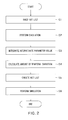
- FIG. 2 is a flow chart showing an example of an operation of the circuit simulating apparatus shown in FIG. 1 .
- FIG. 3 shows schematic diagrams for illustrating an example of an operation of the circuit simulating apparatus shown in FIG. 1 . More specifically, FIG. 3A is a diagram showing an equivalent circuit model of a MOS transistor before degradation of a threshold voltage. FIG. 3B is a diagram showing an equivalent circuit model of the MOS transistor after degradation of the threshold voltage.
- FIG. 4 shows time charts for illustrating an example of an operation of the circuit simulating apparatus shown in FIG. 1 .
- the computing device 13 executes the circuit simulator read from the storage device 11 to read the net list created by the input device 12 from a storage part for the net list.
- the storage part for the net list may be a storage area of the input device 12 , a storage area of the computing device 13 , or a storage area of the storage device 11 .
- the computing device 13 executes the circuit simulator to perform the circuit simulation based on the net list read in the first step (S 1 ).
- the computing device 13 performs a transient analysis.
- the computing device 13 monitors the voltage (voltage stress) and current (current stress) applied to a terminal of a circuit element, for example, for a certain time specified in the net list.
- the result of the transient analysis is an operational condition of the circuit element.
- the computing device 13 executes the circuit simulating program read from the storage device 11 to calculate an intermediate parameter value based on the operational condition of the circuit element shown by the result of the transient analysis.
- the computing device 13 takes into consideration an attenuation of the intermediate parameter value caused by turning off the stress equal to or higher than a reference value.
- the computing device 13 can solve the operational condition based on the result of the transient analysis as described above.
- the computing device 13 may solve the operational condition based on an input result of the input device 12 (for example, the result of setting of on/off time of the element).
- the intermediate parameter value calculated in the second step (S 2 ) is a corrected integrated quantity obtained by subtracting the amount of decrease caused by turning off the stress equal to or higher than the reference value from a reference integrated quantity obtained by integrating a physical quantity of the circuit element determined by the operational condition over a period from a reference time to a calculation time at which the intermediate parameter value is calculated.
- the reference time may be a time at which the stress equal to or higher than the reference value to the circuit element is started, although the reference time is not limited to this time.
- Examples of the intermediate parameter value defined as the corrected integrated quantity include “Qgate”, “Qsub”, and “Age” described below, for example.
- Qgate is a corrected integrated value obtained by subtracting the amount of decrease of the integrated value of a current “Igate” (physical quantity) flowing to a gate of the MOS transistor caused by turning off the voltage stress equal to or higher than the reference value from a reference integrated value obtained by integrating “Igate” over a period from the reference time to the calculation time for “Qgate”.
- the voltage stress is a gate-source voltage “Vgs” or a drain-source voltage “Vds”, for example.
- the reference value of the voltage stress can be any value below which the current “Igate” does not occur.
- the amount of decrease of the integrated value of “Igate” is a value that increases according to an exponential function including a coefficient and a time constant with time during the period of the operational condition that the voltage stress equal to or higher than the reference value is turned off.
- “Qgate” decreases (damps) according to the exponential function with time during the period of the operational condition that the voltage stress equal to or higher than the reference value is turned off.
- Quadratic function does not exclusively decrease according to the exponential function but may decrease according to a linear function, a quadratic function or a function of higher order.
- a second operational condition that the voltage stress equal to or higher than the reference value is applied may occur after the first operational condition that the voltage stress equal to or higher than the reference value is turned off.
- the amount of decrease of the integrated value of “Igate” with respect to the reference integrated value is a constant value, for example.
- the constant value is equal to the amount of decrease of the integrated value of “Igate” at the end of the first operational condition, for example.
- Qgate can be expressed as a function of “Igate” by the following formula.
- Q gate f ( I gate, . . . ) (1)
- Qgate can be used for calculation of the aging degradation ⁇ Vth of the threshold voltage, for example.
- Qgate_a is a constant value under the operational condition that the voltage stress equal to or higher than the reference value is turned off. This is because, in the period in which the voltage stress equal to or higher than the reference value is turned off, “Igate” does not occur, so that the reference integrated value does not increase or decrease.
- Qgate assumes the corrected integrated value that takes into consideration the amount of decrease of the integrated value of “Igate” caused by the recovery characteristics, so that ⁇ Vth obtained based on “Qgate” can represent the recovery characteristics. This will be described in further detail below.
- Qgate can represent such a charge diffusion behavior as an attenuation of “Qgate”, and therefore, ⁇ Vth obtained based on “Qgate” can appropriately represent the recovery characteristics.
- Qsub is a corrected integrated value obtained by subtracting the amount of decrease of the integrated value of a substrate current “Isub” (physical quantity) flowing to a bulk (substrate) node of the MOS transistor caused by turning off the voltage stress equal to or higher than the reference value from a reference integrated value obtained by integrating “Isub” over a period from the reference time to the calculation time for “Qsub”.
- Isub substrate current
- Specific examples of the voltage stress can be the same as those for “Qgate”.
- Specific examples of the amount of decrease can be the same as those for “Qgate”. That is, “Qsub” can decrease according to an exponential function including a coefficient and a time constant with lapse of time during the period of the operational condition that the voltage stress equal to or higher than the reference value is turned off.
- Qsub can be expressed as a function of “Isub” by the following formula.
- Q sub f ( I sub, . . . ) (2)
- Qsub can be used for calculation of the aging degradation ⁇ Vth of the threshold voltage, for example.
- Qsub assumes the corrected integrated value that takes into consideration the amount of decrease of the integrated value of “Isub” caused by the recovery characteristics, so that ⁇ Vth obtained based on “Qsub” can represent the recovery characteristics.
- Age is a corrected age parameter obtained by subtracting the amount of decrease caused by turning off the voltage stress equal to or higher than the reference value from a reference age parameter expressed as a function (integrated quantity) of at least one (physical quantity) of terminal voltage, temperature and element size and the calculation time at which “Age” is calculated.
- Specific examples of the stress can be the same as those for “Qgate”. Specific examples of the amount of decrease can be the same as those for “Qgate”. That is, “Age” can decrease according to an exponential function including a coefficient and a time constant with time during the period of the operational condition that the voltage stress equal to or higher than the reference value is turned off.
- “Age” can be used for calculation of the aging degradation ⁇ Vth of the threshold voltage, for example.
- the reference age parameter can be a constant value under the operational condition that the stress equal to or higher than the reference value is turned off.
- a reference age parameter that assumes a constant value does not take into consideration the amount of decrease caused by the recovery characteristics of the MOS transistor. Therefore, ⁇ Vth obtained based on the reference age parameter cannot represent the recovery characteristics.
- Age is the corrected age parameter that takes into consideration the amount of decrease caused by the recovery characteristics, so that ⁇ Vth obtained based on “Age” can represent the recovery characteristics.
- the third step (S 3 ) is performed.
- the computing device 13 executes the circuit simulating program to calculate an integrated value of the intermediate parameter value calculated in the second step (S 2 ).
- the computing device 13 calculates the total sum of the intermediate parameter value for the aging time. For example, the computing device 13 may calculates the total sum of the intermediate parameter value for a year of continuous operation of the transient analysis described above.
- the computing device 13 In calculating the integrated value of the intermediate parameter value, the computing device 13 naturally takes into consideration the attenuation of the intermediate parameter value because the attenuation of the intermediate parameter value is taken into consideration in the second step (S 2 ).
- this embodiment does not exclude an implementation in which the intermediate parameter value is calculated in the second step (S 2 ) without taking the attenuation into consideration, and then the intermediate parameter value is corrected by taking the attenuation into consideration and the corrected intermediate parameter value is integrated in the third step (S 3 ).
- the computing device 13 calculates the aging degradation of the electrical characteristics of the circuit element based on the integrated value of the intermediate parameter value calculated in the third step (S 3 ).
- the computing device 13 calculates ⁇ Vth that is expressed as a function of “Qgate” and time “T” according to the following formula.
- ⁇ Vth g ( Q gate, T , . . . ) (4)
- the computing device 13 calculates ⁇ Vth that is expressed as a function of “Qsub” and time “T” according to the following formula.
- ⁇ Vth g ( Q sub, T , . . . ) (5)
- the computing device 13 calculates ⁇ Vth that is expressed as a function of “Age” and time “T” according to the following formula.
- ⁇ Vth g (Age, T , . . . ) (6)
- the computing device 13 outputs the calculated aging degradation of the electrical characteristics to the output device 14 .
- the output device 14 outputs the aging degradation of the electrical characteristics received from the computing device 13 in a manner that the analyzer can readily solve the aging degradation.
- the output device 14 may display the aging degradation of the electrical characteristics in the form of a text file or on a circuit diagram data screen.
- the computing device 13 creates a net list in such a manner that the electrical characteristics after the aging degradation, that is, after the aging degradation, can be reproduced by the circuit simulator.
- the computing device 13 stores the created net list in the storage device 11 , for example.
- the way in which the net list represents the electrical characteristics after the aging degradation is not particularly limited.
- the electrical characteristics may be represented by a description with a parameter value by the circuit simulator, or may be represented by an additional equivalent circuit model that represents the amount of degradation.
- a voltage source connected in series with the gate of the MOS transistor which represents the amount of degradation of the threshold voltage, may be added as shown in FIG. 3B .
- the computing device 13 executes the circuit simulator to perform a circuit simulation of the characteristics after aging by using the net list created in the fifth step (S 5 ).
- the characteristics after aging that reflects the recovery characteristics can be checked. If the circuit simulation of the characteristics after aging is performed without taking the recovery characteristics into consideration, the simulation result shows characteristics that are more significantly deteriorated than the actual characteristics. If the circuit is designed based on such a simulation result so that the degradation falls within the allowable limit, circuit elements are inevitably designed to have larger sizes than required in order to allow for the degradation that is more significant than the actual degradation. As a result, the manufacturing cost of the circuit elements unnecessarily increases.
- the circuit simulation of the characteristics can be performed by taking the recovery characteristics into consideration, so that compact circuit elements that allow for the actual degradation can be used, and therefore, the manufacturing cost can be reduced.
- FIG. 4 shows a time chart of the voltage (voltage stress) applied to the circuit element as an example of the operational condition.
- a high-level voltage “VH” corresponds to the stress equal to or higher than the reference value
- a low-level voltage “VL” corresponds to the stress lower than the reference value.
- a period from a time “t 2 ” to a time “t 3 ” in which the low-level voltage “VL” is applied that follows a period from a time “t 1 ” to a time “t 2 ” in which the high-level voltage “VH” is applied for the first time corresponds to the period in which the stress equal to or higher than the reference value is turned off.
- the middle part of FIG. 4 shows a time chart of the integrated value of the intermediate parameter value calculated in the third step (S 3 ) in FIG. 2 .
- the time chart is temporally aligned with the time chart of the applied voltage shown in the upper part of FIG. 4 .
- the solid line shows the integrated value of the intermediate parameter value that takes the attenuation of the intermediate parameter value into consideration described with regard to the second step (S 2 ) and the third step (S 3 ) in FIG. 2 .
- the dashed line shows the integrated value of the intermediate parameter value that does not take the attenuation of the intermediate parameter value into consideration.
- the lower part of FIG. 4 shows a time chart of the aging degradation of the electrical characteristics of the circuit element calculated in the fourth step (S 4 ) in FIG. 2 .
- the time chart is temporally aligned with the time chart of the applied voltage shown in the upper part of FIG. 4 and the time chart of the integrated value of the intermediate parameter value shown in the middle part of FIG. 4 .
- the solid line shows the aging degradation of the electrical characteristics based on the integrated value of the intermediate parameter value that takes the attenuation of the intermediate parameter value into consideration (shown by the solid line in the middle part of FIG. 4 ).
- the dashed line shows the aging degradation of the electrical characteristics based on the integrated value of the intermediate parameter value that does not take the attenuation of the intermediate parameter value into consideration (shown by the dashed line in the middle part of FIG. 4 ).
- the integrated value of the intermediate parameter value monotonically increases with time. This means that, in the period from the time “t 1 ” to the time “t 2 ”, the intermediate parameter value itself monotonically increases with time.
- the integrated value of the intermediate parameter value that takes the attenuation of the intermediate parameter value into consideration (shown by the solid line) damps with time.
- the intermediate parameter value itself damps with time according to an exponential function including a coefficient and a time constant.
- the integrated value of the intermediate parameter value that does not take the attenuation of the intermediate parameter value into consideration (shown by the dashed line) is constant.
- the intermediate parameter value itself is also constant.
- both the integrated value of the intermediate parameter value that takes the attenuation of the intermediate parameter value into consideration (shown by the solid line) and the integrated value of the intermediate parameter value that does not take the attenuation of the intermediate parameter value into consideration (shown by the dashed line) monotonically increase with time.
- the integrated value of the intermediate parameter value that takes the attenuation of the intermediate parameter value into consideration is smaller than the integrated value of the intermediate parameter value that does not take the attenuation of the intermediate parameter value into consideration by a certain amount. This is because, in the period from the time “t 2 ” to the time “t 3 ”, the integrated value of the intermediate parameter value that takes the attenuation of the intermediate parameter value into consideration damps, while the integrated value of the intermediate parameter value that does not take the attenuation of the intermediate parameter value into consideration is constant.
- the magnitude relationship between the integrated values of the intermediate parameter value in the period after the time “t 3 ” shown in FIG. 4 means that, in the period after the time “t 3 ”, the intermediate parameter value that takes the attenuation into consideration can be smaller than the intermediate parameter value that does not take the attenuation into consideration by a certain amount.
- the aging degradation based on the integrated value of the intermediate parameter value that takes the attenuation of the intermediate parameter value into consideration decreases with time.
- the aging degradation properly reflects the recovery characteristics that occur when the applied voltage is set at the low level (“VL”) in the period from the time “t 2 ” to the time “t 3 ”.
- the aging degradation based on the integrated value of the intermediate parameter value that does not take the attenuation of the intermediate parameter value into consideration is constant.
- the aging degradation does not reflect the recovery characteristics in the period from the time “t 2 ” to the time “t 3 ”.
- the intermediate parameter value that reflects the recovery characteristics (a first electrical characteristic value) can be calculated, and therefore, a circuit design that reflects the recovery characteristics can be implemented.
- the semiconductor device including the circuit element designed based on the circuit simulating method can be manufactured.
- the circuit simulating method of the embodiment performs a circuit simulation extremely close to the actual aging degradation of the semiconductor device. Therefore the semiconductor device can be manufactured effectively.
- At least a part of the circuit simulating apparatus may be implemented by hardware or software.
- a program that describes at least a part of the functionality of the data processing method may be stored in a recording medium, such as a flexible disk or CD-ROM, loaded into a computer and executed by the computer.
- the recoding medium is not limited to a removable medium, such as a magnetic disk or an optical disk, but may be a fixed recording medium, such as a hard disk drive or a memory.
- a program that describes at least a part of the functionality of the data processing method may be distributed via a communication line (including radio communication), such as the Internet.
- the program may be encrypted, modulated or compressed and the encrypted, modulated or compressed program may be distributed via wired or wireless communication, such as the Internet, or stored in a recording medium for distribution.
Landscapes
- Engineering & Computer Science (AREA)
- Computer Hardware Design (AREA)
- Physics & Mathematics (AREA)
- Theoretical Computer Science (AREA)
- Evolutionary Computation (AREA)
- Geometry (AREA)
- General Engineering & Computer Science (AREA)
- General Physics & Mathematics (AREA)
- Microelectronics & Electronic Packaging (AREA)
- Design And Manufacture Of Integrated Circuits (AREA)
Abstract
Description
Qgate=f(Igate, . . . ) (1)
Qsub=f(Isub, . . . ) (2)
Age=f(Vds, Vgs, W, L, Temp, . . . ) (3)
ΔVth=g(Qgate, T, . . . ) (4)
ΔVth=g(Qsub, T, . . . ) (5)
ΔVth=g(Age, T, . . . ) (6)
Claims (20)
Applications Claiming Priority (2)
| Application Number | Priority Date | Filing Date | Title |
|---|---|---|---|
| JP2014-183613 | 2014-09-09 | ||
| JP2014183613A JP6434755B2 (en) | 2014-09-09 | 2014-09-09 | Circuit simulation method, circuit simulation apparatus, and computer-readable recording medium |
Publications (2)
| Publication Number | Publication Date |
|---|---|
| US20160070836A1 US20160070836A1 (en) | 2016-03-10 |
| US9495494B2 true US9495494B2 (en) | 2016-11-15 |
Family
ID=55437723
Family Applications (1)
| Application Number | Title | Priority Date | Filing Date |
|---|---|---|---|
| US14/645,309 Expired - Fee Related US9495494B2 (en) | 2014-09-09 | 2015-03-11 | Circuit simulating method, circuit simulating apparatus, and method of manufacturing semiconductor device |
Country Status (2)
| Country | Link |
|---|---|
| US (1) | US9495494B2 (en) |
| JP (1) | JP6434755B2 (en) |
Families Citing this family (1)
| Publication number | Priority date | Publication date | Assignee | Title |
|---|---|---|---|---|
| TWI813421B (en) | 2022-08-19 | 2023-08-21 | 瑞昱半導體股份有限公司 | Method and apparatus for simulating breakdown of electronic component |
Citations (20)
| Publication number | Priority date | Publication date | Assignee | Title |
|---|---|---|---|---|
| JPH06168293A (en) | 1992-12-01 | 1994-06-14 | Nec Corp | Circuit deterioration simulation method |
| JPH08263540A (en) | 1995-03-27 | 1996-10-11 | Hitachi Ltd | Semiconductor device reliability design support system, reliability design method, and semiconductor device designed using the same |
| JPH09292436A (en) | 1996-04-26 | 1997-11-11 | Matsushita Electric Ind Co Ltd | Timing verification method |
| JPH10228497A (en) | 1996-12-11 | 1998-08-25 | Matsushita Electric Ind Co Ltd | Hot carrier deterioration estimation method |
| JP2000011027A (en) | 1998-06-24 | 2000-01-14 | Nec Corp | Method and device for supporting design |
| US6047247A (en) | 1996-12-11 | 2000-04-04 | Matsushita Electric Industrial Co., Ltd. | Method of estimating degradation with consideration of hot carrier effects |
| JP2000339356A (en) | 1999-05-26 | 2000-12-08 | Matsushita Electric Ind Co Ltd | Method and apparatus for simulating hot carrier effects in integrated circuits |
| JP2001036020A (en) | 1999-05-19 | 2001-02-09 | Matsushita Electric Ind Co Ltd | Semiconductor integrated circuit and semiconductor integrated circuit design method |
| US20010029600A1 (en) | 2000-03-30 | 2001-10-11 | Hitachi, Ltd. | Storage media being readable by a computer, and a method for designing a semiconductor integrated circuit device |
| JP2001331545A (en) | 2000-03-17 | 2001-11-30 | Matsushita Electric Ind Co Ltd | Apparatus, calculation method, and inspection method for LSI over time deterioration margin amount |
| US20020022949A1 (en) | 2000-03-17 | 2002-02-21 | Hirokazu Yonezawa | Apparatus and method for calculating temporal deterioration margin amount of LSI, and LSI inspection method |
| US6396307B1 (en) | 1999-05-19 | 2002-05-28 | Matsushita Electric Industrial Co., Ltd. | Semiconductor integrated circuit and method for designing the same |
| JP2003043115A (en) | 2001-08-01 | 2003-02-13 | Matsushita Electric Ind Co Ltd | Method for evaluating characteristics of integrated circuit and method for designing the same |
| JP2003150663A (en) | 2001-11-09 | 2003-05-23 | Toshiba Corp | Evaluation method of semiconductor integrated circuit |
| JP2003188184A (en) | 2001-12-21 | 2003-07-04 | Hitachi Ltd | Semiconductor device simulation method, deterioration degree calculation method, deterioration parameter calculation method, and semiconductor device design method |
| JP2005100458A (en) | 2000-03-17 | 2005-04-14 | Matsushita Electric Ind Co Ltd | LSI inspection method |
| JP2007257524A (en) | 2006-03-24 | 2007-10-04 | Univ Waseda | Circuit operation analysis apparatus and circuit operation analysis method |
| US20080027700A1 (en) | 2006-07-28 | 2008-01-31 | Akinari Kinoshita | Simulation model of BT instability of transistor |
| JP2008042161A (en) | 2006-08-09 | 2008-02-21 | Ind Technol Res Inst | Circuit reliability simulation method and system |
| JP2008225961A (en) | 2007-03-14 | 2008-09-25 | Sanyo Electric Co Ltd | Circuit simulation method |
-
2014
- 2014-09-09 JP JP2014183613A patent/JP6434755B2/en not_active Expired - Fee Related
-
2015
- 2015-03-11 US US14/645,309 patent/US9495494B2/en not_active Expired - Fee Related
Patent Citations (34)
| Publication number | Priority date | Publication date | Assignee | Title |
|---|---|---|---|---|
| JPH06168293A (en) | 1992-12-01 | 1994-06-14 | Nec Corp | Circuit deterioration simulation method |
| JPH08263540A (en) | 1995-03-27 | 1996-10-11 | Hitachi Ltd | Semiconductor device reliability design support system, reliability design method, and semiconductor device designed using the same |
| JPH09292436A (en) | 1996-04-26 | 1997-11-11 | Matsushita Electric Ind Co Ltd | Timing verification method |
| JPH10228497A (en) | 1996-12-11 | 1998-08-25 | Matsushita Electric Ind Co Ltd | Hot carrier deterioration estimation method |
| US6047247A (en) | 1996-12-11 | 2000-04-04 | Matsushita Electric Industrial Co., Ltd. | Method of estimating degradation with consideration of hot carrier effects |
| US6629295B1 (en) | 1998-06-24 | 2003-09-30 | Nec Corporation | Design automation method and device |
| JP2000011027A (en) | 1998-06-24 | 2000-01-14 | Nec Corp | Method and device for supporting design |
| US6498515B2 (en) | 1999-05-19 | 2002-12-24 | Matsushita Electric Industrial Co., Ltd. | Semiconductor integrated circuit and method for designing the same |
| US6396307B1 (en) | 1999-05-19 | 2002-05-28 | Matsushita Electric Industrial Co., Ltd. | Semiconductor integrated circuit and method for designing the same |
| US20020140460A1 (en) | 1999-05-19 | 2002-10-03 | Matsushita Electric Industrial Co., Ltd. | Semiconductor integrated circuit and method for designing the same |
| JP2001036020A (en) | 1999-05-19 | 2001-02-09 | Matsushita Electric Ind Co Ltd | Semiconductor integrated circuit and semiconductor integrated circuit design method |
| JP2000339356A (en) | 1999-05-26 | 2000-12-08 | Matsushita Electric Ind Co Ltd | Method and apparatus for simulating hot carrier effects in integrated circuits |
| JP2001331545A (en) | 2000-03-17 | 2001-11-30 | Matsushita Electric Ind Co Ltd | Apparatus, calculation method, and inspection method for LSI over time deterioration margin amount |
| US20020022949A1 (en) | 2000-03-17 | 2002-02-21 | Hirokazu Yonezawa | Apparatus and method for calculating temporal deterioration margin amount of LSI, and LSI inspection method |
| JP2005100458A (en) | 2000-03-17 | 2005-04-14 | Matsushita Electric Ind Co Ltd | LSI inspection method |
| US6795802B2 (en) | 2000-03-17 | 2004-09-21 | Matsushita Electric Industrial Co., Ltd. | Apparatus and method for calculating temporal deterioration margin amount of LSI, and LSI inspection method |
| US20010029600A1 (en) | 2000-03-30 | 2001-10-11 | Hitachi, Ltd. | Storage media being readable by a computer, and a method for designing a semiconductor integrated circuit device |
| JP2001284457A (en) | 2000-03-30 | 2001-10-12 | Hitachi Ltd | Computer-readable storage medium and semiconductor device design method |
| US20010032329A1 (en) | 2000-03-30 | 2001-10-18 | Hitachi, Ltd. | Storage media being readable by a computer, and a method for designing a semiconductor integrated circuit device |
| US6634015B2 (en) | 2000-03-30 | 2003-10-14 | Hitachi, Ltd. | Computer-readable storage media stored with a delay library for designing a semiconductor integrated circuit device |
| JP2003043115A (en) | 2001-08-01 | 2003-02-13 | Matsushita Electric Ind Co Ltd | Method for evaluating characteristics of integrated circuit and method for designing the same |
| US6869808B2 (en) | 2001-08-01 | 2005-03-22 | Matsushita Electric Industrial Co., Ltd. | Method for evaluating property of integrated circuitry |
| US20030054577A1 (en) | 2001-08-01 | 2003-03-20 | Matsushita Electric Industrial Co., Ltd. | Method for evaluating property of integrated circuit and method for designing the same |
| US20030188277A1 (en) | 2001-11-09 | 2003-10-02 | Hideaki Murakami | Method of evaluating semiconductor integrated circuit to be designed in consideration of standby DC leakage current |
| JP2003150663A (en) | 2001-11-09 | 2003-05-23 | Toshiba Corp | Evaluation method of semiconductor integrated circuit |
| US6810509B2 (en) | 2001-11-09 | 2004-10-26 | Kabushiki Kaisha Toshiba | Method of evaluating semiconductor integrated circuit to be designed in consideration of standby DC leakage current |
| JP2003188184A (en) | 2001-12-21 | 2003-07-04 | Hitachi Ltd | Semiconductor device simulation method, deterioration degree calculation method, deterioration parameter calculation method, and semiconductor device design method |
| JP2007257524A (en) | 2006-03-24 | 2007-10-04 | Univ Waseda | Circuit operation analysis apparatus and circuit operation analysis method |
| US20080027700A1 (en) | 2006-07-28 | 2008-01-31 | Akinari Kinoshita | Simulation model of BT instability of transistor |
| JP2008053692A (en) | 2006-07-28 | 2008-03-06 | Matsushita Electric Ind Co Ltd | Simulation model of BT degradation of transistor and simulation modeling method |
| US8271254B2 (en) | 2006-07-28 | 2012-09-18 | Panasonic Corporation | Simulation model of BT instability of transistor |
| JP2008042161A (en) | 2006-08-09 | 2008-02-21 | Ind Technol Res Inst | Circuit reliability simulation method and system |
| US20080126064A1 (en) | 2006-08-09 | 2008-05-29 | Industrial Technology Research Institute | Method for simulating circuit reliability and system thereof |
| JP2008225961A (en) | 2007-03-14 | 2008-09-25 | Sanyo Electric Co Ltd | Circuit simulation method |
Non-Patent Citations (7)
Also Published As
| Publication number | Publication date |
|---|---|
| US20160070836A1 (en) | 2016-03-10 |
| JP2016057841A (en) | 2016-04-21 |
| JP6434755B2 (en) | 2018-12-05 |
Similar Documents
| Publication | Publication Date | Title |
|---|---|---|
| US12223246B2 (en) | Systems, methods, and computer program products for transistor compact modeling using artificial neural networks | |
| US20200151294A1 (en) | Method for generating aging model and manufacturing semiconductor chip using the same | |
| US8606557B2 (en) | Table lookup method for physics based models for SPICE-like simulators | |
| US20150154331A1 (en) | Estimating delay deterioration due to device degradation in integrated circuits | |
| US9141735B2 (en) | Circuit device reliability simulation system | |
| US10977402B2 (en) | Circuit testing and manufacture using multiple timing libraries | |
| KR102424369B1 (en) | Method of Predicting Reliability Failure Rate of Semiconductor Integrated Circuit And Device There-of | |
| US8527921B2 (en) | Constrained random simulation coverage closure guided by a cover property | |
| US7983889B2 (en) | Simulation method and simulation apparatus for LDMOSFET | |
| US20160112041A1 (en) | Power transistor model | |
| US9495494B2 (en) | Circuit simulating method, circuit simulating apparatus, and method of manufacturing semiconductor device | |
| US8392867B2 (en) | System, method and program storage device for developing condensed netlists representative of groups of active devices in an integrated circuit and for modeling the performance of the integrated circuit based on the condensed netlists | |
| JP2010108360A (en) | Simulation method, information processor, and program | |
| US20150234961A1 (en) | Method and apparatus for circuit reliability aging | |
| Akturk et al. | Compact modeling of 0.35 μm SOI CMOS technology node for 4 K DC operation using Verilog-A | |
| US8650527B2 (en) | Method and software tool for analyzing and reducing the failure rate of an integrated circuit | |
| US7606693B2 (en) | Circuit simulation with decoupled self-heating analysis | |
| CN114004180B (en) | Methods, apparatus, and computer equipment for critical failure path analysis of integrated circuits | |
| US8515715B2 (en) | Method, system and program storage device for simulating electronic device performance as a function of process variations | |
| US8332199B1 (en) | Graphical user interface for viewing intermediate calculations from a device model | |
| US20260056244A1 (en) | Determining an operational limit for a transistor device with aging recovery | |
| US10248753B2 (en) | Pessimism reduction in hierarchical blockage aggressors using estimated resistor and capacitor values | |
| US20240160950A1 (en) | Method and device for processing neural network model for circuit simulator | |
| KR102276908B1 (en) | A computing device executable for a program performing a method for analysing power noise in a semiconductor device, a method including the same for designing a semiconductor device, and a program strorage medium storing the program | |
| JP2013122749A (en) | Circuit operation verification device and verification method for semiconductor integrated circuit |
Legal Events
| Date | Code | Title | Description |
|---|---|---|---|
| AS | Assignment |
Owner name: KABUSHIKI KAISHA TOSHIBA, JAPAN Free format text: ASSIGNMENT OF ASSIGNORS INTEREST;ASSIGNORS:KIMURA, TOMOHISA;ABE, KAZUHIDE;SIGNING DATES FROM 20150302 TO 20150303;REEL/FRAME:035144/0692 |
|
| STCF | Information on status: patent grant |
Free format text: PATENTED CASE |
|
| MAFP | Maintenance fee payment |
Free format text: PAYMENT OF MAINTENANCE FEE, 4TH YEAR, LARGE ENTITY (ORIGINAL EVENT CODE: M1551); ENTITY STATUS OF PATENT OWNER: LARGE ENTITY Year of fee payment: 4 |
|
| LAPS | Lapse for failure to pay maintenance fees |
Free format text: PATENT EXPIRED FOR FAILURE TO PAY MAINTENANCE FEES (ORIGINAL EVENT CODE: EXP.); ENTITY STATUS OF PATENT OWNER: LARGE ENTITY |
|
| STCH | Information on status: patent discontinuation |
Free format text: PATENT EXPIRED DUE TO NONPAYMENT OF MAINTENANCE FEES UNDER 37 CFR 1.362 |
|
| FP | Lapsed due to failure to pay maintenance fee |
Effective date: 20241115 |