US9490928B2 - Arrayed waveguide grating based modular interconnection networks and methods for constructing and applying the same - Google Patents
Arrayed waveguide grating based modular interconnection networks and methods for constructing and applying the same Download PDFInfo
- Publication number
- US9490928B2 US9490928B2 US14/557,429 US201414557429A US9490928B2 US 9490928 B2 US9490928 B2 US 9490928B2 US 201414557429 A US201414557429 A US 201414557429A US 9490928 B2 US9490928 B2 US 9490928B2
- Authority
- US
- United States
- Prior art keywords
- wavelength
- awg
- port
- nodes
- ports
- Prior art date
- Legal status (The legal status is an assumption and is not a legal conclusion. Google has not performed a legal analysis and makes no representation as to the accuracy of the status listed.)
- Active
Links
Images


Classifications
-
- H—ELECTRICITY
- H04—ELECTRIC COMMUNICATION TECHNIQUE
- H04J—MULTIPLEX COMMUNICATION
- H04J14/00—Optical multiplex systems
- H04J14/02—Wavelength-division multiplex systems
- H04J14/0227—Operation, administration, maintenance or provisioning [OAMP] of WDM networks, e.g. media access, routing or wavelength allocation
- H04J14/0254—Optical medium access
- H04J14/0267—Optical signaling or routing
-
- H—ELECTRICITY
- H04—ELECTRIC COMMUNICATION TECHNIQUE
- H04J—MULTIPLEX COMMUNICATION
- H04J14/00—Optical multiplex systems
- H04J14/02—Wavelength-division multiplex systems
- H04J14/0278—WDM optical network architectures
- H04J14/0279—WDM point-to-point architectures
-
- H—ELECTRICITY
- H04—ELECTRIC COMMUNICATION TECHNIQUE
- H04L—TRANSMISSION OF DIGITAL INFORMATION, e.g. TELEGRAPHIC COMMUNICATION
- H04L49/00—Packet switching elements
-
- H—ELECTRICITY
- H04—ELECTRIC COMMUNICATION TECHNIQUE
- H04Q—SELECTING
- H04Q11/00—Selecting arrangements for multiplex systems
- H04Q11/0001—Selecting arrangements for multiplex systems using optical switching
- H04Q11/0005—Switch and router aspects
- H04Q2011/0007—Construction
- H04Q2011/0016—Construction using wavelength multiplexing or demultiplexing
-
- H—ELECTRICITY
- H04—ELECTRIC COMMUNICATION TECHNIQUE
- H04Q—SELECTING
- H04Q11/00—Selecting arrangements for multiplex systems
- H04Q11/0001—Selecting arrangements for multiplex systems using optical switching
- H04Q11/0005—Switch and router aspects
- H04Q2011/0007—Construction
- H04Q2011/0032—Construction using static wavelength routers (e.g. arrayed waveguide grating router [AWGR] )
Definitions
- the present invention relates to large-scale networking of a data center, and in particular, relates to an arrayed waveguide grating (AWG) based modular interconnection network and methods for constructing and applying the same.
- AWG arrayed waveguide grating
- each data center of Amazon has about 60,000 servers, and that for Google, the number exceeds 50,000 servers, while Microsoft is building a data center containing over 300,000 servers.
- Current data centers generally adopt the layered tree topology, such as the ‘Fat Tree’ topology.
- the advantage of the tree topology is its large bi-directional bandwidth, while the disadvantage is its lack of scalability.
- topological and cabling complexity in data centers is reaching unimaginable proportions, leading to maintenance challenges, inefficient cooling, and substantial operational costs.
- the first is to replace wires with wireless interconnects.
- Wireless networking has signals prone to interference, small bandwidth, and high consumption of stations, making it only a topic at the academies, and not fit for practical application.
- the second is to develop a unified structure based on integrated and enhanced Ethernets, with Cisco and Brocade being the major proponents.
- Cisco and Brocade being the major proponents.
- the method decreases the number of cables, trunk adapters, and network interfaces, the cost of equipping and integrating network adapters is huge, further, main boards for Ethernet optical fiber channels are not yet available.
- the third is to adopt structured cabling.
- the main idea is to divide the cabling system in a data center into a main cabling area and a device area based on different devices.
- the main cabling area and the device area are connected with optical cables, while servers, switchers, and storage devices are jumper-connected via cable distribution frames in the main cabling area and the device area.
- the proposed solution simplifies cable management to some extent, making it possible to move or modify the system by merely changing jumpers. But it does not decrease the number of system cables, thus interconnecting complexity remains and the operating difficulty is still high.
- the present invention solves the problem of the cabling complexity and related management issues by providing a design method of AWG-based modular interconnection networks to reduce cabling complexity so as to simplify networking maintenance and management.
- the present invention provides an AWG-based modular interconnection network comprising left nodes, the number of the left nodes being N 1 , with each left node having N 2 ports; right nodes, the number of the right nodes being N 2 , with each right node having N 1 ports; N 1 and N 2 each representing a positive integer, N 1 ⁇ N 2 , and N 1 and N 2 having a greatest common divisor r, and each port having an optical transceiver associated with a fixed wavelength, characterized in that it further comprises:
- N 2 ⁇ 1 wavelength multiplexers the number of the N 2 ⁇ 1 wavelength multiplexers being N 1 , with each of the N 2 ⁇ 1 wavelength multiplexers having N 2 input ports being respectively connected with the N 2 ports of each of the left nodes;
- the present invention further provides an AWG-based modular interconnection network, comprising left nodes, the number of the left nodes being N 1 , with each of the left nodes having N 2 ports, right nodes, the number of the right nodes being N 2 , with each of the right nodes having N 1 ports;
- N 1 and N 2 are integers, N 1 ⁇ N 2 , N 1 and N 2 having the greatest common divisor r, and each port having an optical transceiver associated with a fixed wavelength, characterized in that it further comprises:
- N 1 n 2 stands for the product of N 1 and n 2 , and same goes for the same styled numbers in the subject application
- n 1 N 1 /r
- r ⁇ r AWGs connecting the r ⁇ 1 wavelength multiplexers and the 1 ⁇ r wavelength demultiplexers, the number of the r ⁇ r AWGs being n 1 n 2 , and each of the r ⁇ r AWGs being associated with a wavelength subset ⁇ k
- k 0, 1, . . . , r ⁇ 1 ⁇ .
- N 2 ⁇ 1 wavelength multiplexers the number of the N 2 ⁇ 1 wavelength multiplexers being N 1 , each of the N 2 ⁇ 1 wavelength multiplexers having N 2 input ports respectively connected with the N 2 ports of each of the left nodes;
- N 2 ⁇ N 2 AWGs connecting the N 2 ⁇ 1 wavelength multiplexers and the 1 ⁇ N 2 wavelength demultiplexers, the number of the N 2 ⁇ N 2 AWGs being K, each of the N 2 ⁇ N 2 AWGs being associated with a wavelength subset ⁇ k
- k 0, 1, . . . , N 2 ⁇ 1 ⁇ .
- the present invention further provides a method for constructing an AWG-based modular interconnection network having N 1 left nodes, with each left node having N 2 ports; the N 2 right nodes, with each right node having N 1 ports; N 1 ⁇ N 2 , N 1 and N 2 being integers having a greatest common divisor r; and each port having an optical transceiver associated with a fixed wavelength, characterized in that the method comprises the following steps:
- Step 1 providing N 1 N 2 ⁇ 1 wavelength multiplexers, labeled by L 0 , L 1 , . . . , L N 1 ⁇ 1 , for the N 1 left nodes, the ith N 2 ⁇ 1 wavelength multiplexer having its jth input port connected with the jth port of the ith left node, and the jth port of the ith left node is associated with wavelength
- Step 2 providing N 2 1 ⁇ N 1 wavelength demultiplexers labeled by R 0 , R 1 , . . . , R N 2 ⁇ 1 , for N 2 right nodes, the jth 1 ⁇ N 1 wavelength demultiplexer having its ith output port connected separately with the ith port of the jth right node, and the ith port of the jth right node is associated with wavelength
- the method further comprises:
- each of the AWGs in the central stage is labeled by G A1 ( ⁇ A ,b A );
- the ⁇ A th input port of G A1 ( ⁇ A ,b A ) is connected with the b A th output port of D A1 ( ⁇ A ,a A )
- the ⁇ A th output port of G A1 ( ⁇ A ,b A ) is connected with the ⁇ A th input port of M A1 ( ⁇ A ,b A )
- G A1 ( ⁇ A ,b A ) is associated with a wavelength subset ⁇ [ ⁇ ⁇ +b ⁇
- Step 5 substituting the ith N 2 ⁇ 1 wavelength multiplexer L i and the 1 ⁇ n 2 wavelength demultiplexer D A1 ( ⁇ A ,a A ) with n 2 r ⁇ 1 wavelength multiplexers, each of which is labeled by D A2 ( ⁇ A ,a A ,b A );
- the method further comprises:
- k 0, 1, .
- the a B th input port of G B1 ( ⁇ B ) is thus D B1 ( ⁇ B ,a B ), the ⁇ B th output port of G B1 ( ⁇ B ) is connected with the ⁇ B th input port of M B1 ( ⁇ B );
- Step 5 denoting each of the N 1 ⁇ 1 wavelength multiplexers as D B2 ( ⁇ B ,a B );
- D B2 ( ⁇ B ,a B ) is connected with the a B th input port of G B2 ( ⁇ B ), and M B2 ( ⁇ B , ⁇ B ) is connected with the ⁇ B th output port of G B2 ( ⁇ B ).
- the method further comprises:
- Step 6 in the case of the dimension of the AWG in the central stage still being large, returning to Step 4, and substituting the AWG in the central stage with a module constituted of a three-stage network of small AWGs.
- the present invention further provides an application of AWGs in an interconnection network. Compared with the previous works, the present invention has the following advantages:
- Wavelengths are reused in the AWG-based interconnection network, i.e., the r ⁇ r AWGs in the network reuses the same wavelength subset ⁇ 0 , . . . , ⁇ r ⁇ 1 ⁇ , which improves the scalability of the AWG-based interconnection system.
- Step 4 can be employed to decompose the r ⁇ r AWG into an r ⁇ r three-stage AWG network.
- FIG. 1 shows an N 1 ⁇ N 2 interconnection network 1 of the present invention
- FIG. 2 shows an AWG-based N 1 ⁇ N 2 interconnection network 2 of the present invention
- FIG. 3 shows an N 1 ⁇ N 2 interconnection network A1 comprising a three-stage AWG network S A of the present invention
- FIG. 4 shows a KN 2 ⁇ N 2 interconnection network B1 comprising a two-stage AWG network S B of the present invention
- FIG. 5 shows an N 1 ⁇ N 2 AWG-based modular interconnection network A2 of the present invention
- FIG. 6 shows a KN 2 ⁇ N 2 AWG-based modular interconnection network B2 of the present invention
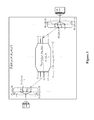
- FIG. 7 shows a 15 ⁇ 10 interconnection network 1 of the present invention
- FIG. 8 shows a 15 ⁇ 10 AWG-based interconnection network 2 of the present invention
- FIG. 9 shows a 15 ⁇ 10 interconnection network A1 comprising an AWG network S A of the present invention.
- FIG. 10 shows a 15 ⁇ 10 AWG-based modular interconnection network A2 of the present invention
- FIG. 11 shows a 12 ⁇ 6 interconnection network 1 of the present invention
- FIG. 12 shows a 12 ⁇ 6 AWG-based interconnection network 2 of the present invention
- FIG. 13 shows a 12 ⁇ 6 AWG-based interconnection network B1 comprising a two-stage AWG network S B of the present invention
- FIG. 14 shows a 12 ⁇ 6 AWG-based modular interconnection network B2 of the present invention.
- An N 1 ⁇ N 2 (N 1 ⁇ N 2 , and N 1 and N 2 having a maximum divisor r) interconnection network 1 contains N 1 left nodes, with each node comprising N 2 ports, and each port having an optical transceiver; N 2 right nodes, with each node comprising N 1 ports, and each port having an optical transceiver. All the optical transceivers are associated with the same wavelength ⁇ 0 . For each of the paired left node and right node, there is one and only one link between them, and thus, there are altogether N 1 N 2 links in the interconnection network, as shown in FIG. 1 , where the small block on each port of the node represents an optical transceiver.
- An AWG-based modular interconnection network for reducing the cabling complexity of a data center mainly via the wavelength division multiplexing property of AWGs comprises the following parameters:
- N 1 ⁇ 1 wavelength multiplexer/demultiplexer N 1 ⁇ 1 AWG;
- N 2 ⁇ 1 wavelength multiplexer/demultiplexer N 2 ⁇ 1 AWG
- n 1 ⁇ 1 wavelength multiplexer/demultiplexer n 1 ⁇ 1 AWG
- n 2 ⁇ 1 wavelength multiplexer/demultiplexer n 2 ⁇ 1 AWG
- KN 2 ⁇ N 2 AWG network S B (K, N 2 , K, 1, N 2 ): an AWG network, with K N 2 ⁇ N 2 AWGs in the first stage, and N 2 K ⁇ 1 multiplexers in the second stage, as shown in FIG. 4 ;
- N 1 ⁇ N 2 interconnection network 2 N 1 left nodes and N 1 N 2 ⁇ 1 multiplexers on the left side, N 2 right nodes and N 2 1 ⁇ N 1 demultiplexers on the right side, and an N 1 ⁇ N 2 AWG on the central stage;
- N 1 ⁇ N 2 interconnection network A1 consists of N 1 left nodes and N 1 N 2 ⁇ 1 multiplexers, N 2 right nodes and N 2 1 ⁇ N 1 demultiplexers, and an N 1 ⁇ N 2 AWG network S A on the central stage, as shown in FIG. 3 ;
- N 1 ⁇ N 2 interconnection network B1 consists of N 1 left nodes and N 1 N 2 ⁇ 1 multiplexers; N 2 right nodes and N 2 1 ⁇ N 1 demultiplexers, and an N 1 ⁇ N 2 AWG network S B on the central stage, as shown in FIG. 4 ;
- N 1 ⁇ N 2 interconnection network A2 consists of N 1 left nodes and N 1 n 2 r ⁇ 1 multiplexers, N 2 right nodes and N 2 n 1 1 ⁇ r demultiplexers, and n 1 n 2 identical r ⁇ r AWGs on the central stage, as shown in FIG. 5 ;
- N 1 ⁇ N 2 interconnection network B2 consists of N 1 left nodes and N 1 N 2 ⁇ 1 multiplexers, N 2 right nodes and KN 2 1 ⁇ N 1 demultiplexers, and K identical N 2 ⁇ N 2 AWGs on the central stage, as shown in FIG. 6 .
- a method of construction of an AWG-based modular interconnection network comprises the following steps:
- N 1 N 2 ⁇ 1 wavelength multiplexers labeled by L 0 , L 1 , . . . , L N 1 ⁇ 1 for N 1 left nodes
- N 2 ⁇ 1 provide N 2 1 ⁇ N 1 wavelength demultiplexers labeled by R 0 , R 1 , . . . , R N 2 -1, for N 2 right nodes, the jth 1 ⁇ N 1 wavelength demultiplexer having its ith output port connected separately with the ith port of the jth right node, and the ith port of the jth right node is associated with wavelength ⁇ [i+r] N1 .
- Use N 1 ⁇ N 2 AWG to connect N 1 N 2 ⁇ 1 wavelength multiplexers on the left with N 2 1 ⁇ N 1 wavelength demultiplexers on the right. This step transforms the 1 into an 2 , with all the optical fibers being replaced by an AWG, as shown in FIG. 2 , where the ith left node connects with the jth right node through wavelength ⁇ [i+j] N1 .
- G A1 (a A ,b A ) an AWG in the central stage is labeled by G A1 (a A ,b A );
- the ⁇ A th port of G A1 (a A ,b A ) is connected with the bath port of D A1 ( ⁇ A ,a A )
- the ⁇ A th port of G A1 (a A ,b A ) is connected with the a A th port of M A1 ( ⁇ A ,b A )
- This step transforms 2 to A1 , in which the ith left node connects with the jth right node via wavelength ⁇ [a A +b A ] n1 r+[ ⁇ A + ⁇ A ] r along the path as follows:
- the three-stage network S A degenerates into a two-stage network S B (K,N 2 ,K,1,N 2 ), where each input port degenerates into a 1 ⁇ 1 demultiplexer, i.e., a fiber link, the dimension of the AWGs in the central stage is N 2 ⁇ N 2 , and each output port becomes a K ⁇ 1 multiplexer.
- k 0, 1, . . .
- Wavelengths are precious resources in an optical communication window, and the number of wavelengths required by the system should not increase with the dimension of the interconnection network, and therefore, wavelength reuse must be taken into account.
- each r ⁇ r AWG can reuse the same wavelength subset ⁇ k
- k 0, 1, . . . , r ⁇ 1 ⁇ .
- the r ⁇ r AWG in the central stage is labeled by G A2 (a A ,b A ).
- the output port of D A2 ( ⁇ A ,a A ,b A ) is connected with the ⁇ A th input port of G A2 (a A ,b A ), and the input port of M A2 ( ⁇ A ,b A ,a A ) is connected with the ⁇ A th output port of G A2 (a A ,b A ).
- A1 is transformed into A2 , where the ith left node connects with the jth right node via wavelength ⁇ [ ⁇ A + ⁇ A ] r , along the path as follows:
- step (2) substitute the ith 1 ⁇ N 1 demultiplexer R j on the right side of B1 and the jth K ⁇ 1 multiplexer M B1 ( ⁇ B ) on the output side of S B with K N 2 ⁇ 1 demultiplexers, each of which is labeled by M B2 ( ⁇ B , ⁇ B ).
- M B2 ⁇ B , ⁇ B
- Each N 2 ⁇ N 2 AWG in the central stage is labeled by G B2 ( ⁇ B ) and can be associated with the same wavelength subset ⁇ k
- k 0, 1, . . . , N 2 ⁇ 1 ⁇ .
- the input port is labeled by D B2 ( ⁇ B ,a B ).
- D B2 ( ⁇ B ,a B ) is connected with the a B th input port of G B2 ( ⁇ B ), and M B2 ( ⁇ B , ⁇ B ) is connected with the ⁇ B th output port of G B2 ( ⁇ B ).
- B1 is transformed into B2 , in which the ith left node connects with the jth right node via wavelength ⁇ [ ⁇ B + ⁇ B ]N 2 along the path as follows:
- step (2) If the dimension of the AWG in the central stage is still very large, the method of step (2) can be employed to substitute each AWG in the central stage with a module encapsulated with a three-stage AWG network.
- a method for constructing an AWG-based modular interconnection network is shown. As for a 15 ⁇ 10 interconnection network 1 , as shown in FIG. 7 , where the greatest common divisor of 15 and 10 is 5, the construction method of an AWG-based modular interconnection network comprises the following steps:
- this step transforms 2 into A1 .
- A1 needs only 60 optical fiber links.
- the reduction ratio of the number of required optical fiber links in this example is 2.5;
- the number of optical fiber links is reduced from 150 to 60, and the reduction of the number of optical fiber links remarkably cuts down the network complexity and thus simplifies system maintenance.
- the number of optical fiber links is reduced r/2 times.
- N 1 and N 2 might be very large, which results in that the dimension of the AWGs in the central stage is still large.
- the method in step (2) can be employed to substitute each AWG in the central stage with a module that consists of a three-stage network of small AWGs.
- a method for constructing an AWG-based modular interconnection network, as for a 12 ⁇ 6 interconnection network 1 as shown in FIG. 11 , where 12 is a multiple of 6, the construction comprises the following steps:
- the method in step (2) can be employed to substitute the AWG in the central stage with a module that consists of a three-stage network of small AWGs.
- This is the idea of modulization of the present invention.
- the number of optical fiber links is reduced from 72 to 12, a 6 time reduction.
- N 1 is a multiple of N 2
- the number of optical fiber links can be reduced from N 1 N 2 to N 1 , by employing the method. The reduction of the number of optical fiber links cuts down the network complexity and thus simplifies network maintenance.
Abstract
An arrayed waveguide grating (AWG) based interconnection network and modular construction method, comprising N1 left nodes, with each left node having N2 ports, N2 right nodes, with each right node having N1 ports, where N1≧N2, N1 and N2 having a greatest common divisor r, and each port having an optical transceiver associated with a fixed wavelength; N1n2 r×1 wavelength multiplexers having their input ports respectively connected with the ports of N1 left nodes, where n2=N2/r; N2n1 1×r wavelength demultiplexers having their output ports respectively connected with the ports of N2 right nodes, where n1=N1/r; n1n2 r×r AWGs connecting the r×1 wavelength multiplexers and the 1×r wavelength demultiplexers r×rn1n2, and each of the r×r AWGs being associated with a wavelength subset {λk|k=0, 1, . . . , r−1}.
Description
The subject application claims priority on Chinese patent application No. CN 201410410122.8 filed on Aug. 20, 2014. The contents and subject matter of the Chinese priority application is incorporated herein by reference.
The present invention relates to large-scale networking of a data center, and in particular, relates to an arrayed waveguide grating (AWG) based modular interconnection network and methods for constructing and applying the same.
In the past decade, fast global information development push data centers to evolve along the direction of super large scale. In 2012, each data center of Amazon has about 60,000 servers, and that for Google, the number exceeds 50,000 servers, while Microsoft is building a data center containing over 300,000 servers. Current data centers generally adopt the layered tree topology, such as the ‘Fat Tree’ topology. The advantage of the tree topology is its large bi-directional bandwidth, while the disadvantage is its lack of scalability. As pointed out in the Article entitled “60 GHz Data-Center Networking: Wireless Worry less,” topological and cabling complexity in data centers is reaching unimaginable proportions, leading to maintenance challenges, inefficient cooling, and substantial operational costs.
To tackle the interconnecting issue, the following proposals have been put forth in the industry:
The first is to replace wires with wireless interconnects. Wireless networking has signals prone to interference, small bandwidth, and high consumption of stations, making it only a topic at the academies, and not fit for practical application.
The second is to develop a unified structure based on integrated and enhanced Ethernets, with Cisco and Brocade being the major proponents. Although the method decreases the number of cables, trunk adapters, and network interfaces, the cost of equipping and integrating network adapters is huge, further, main boards for Ethernet optical fiber channels are not yet available.
The third is to adopt structured cabling. The main idea is to divide the cabling system in a data center into a main cabling area and a device area based on different devices. The main cabling area and the device area are connected with optical cables, while servers, switchers, and storage devices are jumper-connected via cable distribution frames in the main cabling area and the device area. The proposed solution simplifies cable management to some extent, making it possible to move or modify the system by merely changing jumpers. But it does not decrease the number of system cables, thus interconnecting complexity remains and the operating difficulty is still high.
Because of the above reasons, a method of module networking based on Arrayed Waveguide Grating (AWG) and directed at cabling complexity and management in a data center is in need.
The present invention solves the problem of the cabling complexity and related management issues by providing a design method of AWG-based modular interconnection networks to reduce cabling complexity so as to simplify networking maintenance and management.
The present invention provides an AWG-based modular interconnection network comprising left nodes, the number of the left nodes being N1, with each left node having N2 ports; right nodes, the number of the right nodes being N2, with each right node having N1 ports; N1 and N2 each representing a positive integer, N1≧N2, and N1 and N2 having a greatest common divisor r, and each port having an optical transceiver associated with a fixed wavelength, characterized in that it further comprises:
N2×1 wavelength multiplexers, the number of the N2×1 wavelength multiplexers being N1, with each of the N2×1 wavelength multiplexers having N2 input ports being respectively connected with the N2 ports of each of the left nodes;
1×N1 wavelength demultiplexers, the number of the 1×N1 wavelength demultiplexers being N2, with each of the 1×N1 wavelength demultiplexers having N1 output ports respectively connected with the N1 ports of each of the right nodes; and
an N1×N2 AWG connecting the N2×1 wavelength multiplexers and the 1×N1 wavelength demultiplexers, the N1×N2 AWG having N1 input ports and N2 output ports, and being associated with a wavelength set Λ={λ0, λ1, . . . , λN 1 −1}.
The present invention further provides an AWG-based modular interconnection network, comprising left nodes, the number of the left nodes being N1, with each of the left nodes having N2 ports, right nodes, the number of the right nodes being N2, with each of the right nodes having N1 ports; N1 and N2 are integers, N1≧N2, N1 and N2 having the greatest common divisor r, and each port having an optical transceiver associated with a fixed wavelength, characterized in that it further comprises:
r×1 wavelength multiplexers, the number of the r×1 wavelength multiplexers being N1n2 (N1n2 stands for the product of N1 and n2, and same goes for the same styled numbers in the subject application), and n2 r×1 wavelength multiplexers having their input ports respectively connected with the N2 ports of one of the left nodes, where n2=N2/r;
1×r wavelength demultiplexers, the number of the 1×r wavelength demultiplexers being N2n1, and n 1 1×r wavelength demultiplexers having output ports respectively connected with the N1 ports of one of the right nodes, where n1=N1/r; and
r×r AWGs connecting the r×1 wavelength multiplexers and the 1×r wavelength demultiplexers, the number of the r×r AWGs being n1n2, and each of the r×r AWGs being associated with a wavelength subset {λk|k=0, 1, . . . , r−1}.
The present invention also provides an AWG-based modular interconnection network, comprising left nodes, the number of the left nodes being N1, with each of the left nodes having N2 ports; right nodes, the number of the right nodes being N2 with each of the right node having N1 ports; N1, N2, and K are integers, where N1=KN2; and each port having an optical transceiver associated with a fixed wavelength, characterized in that it further comprises:
N2×1 wavelength multiplexers, the number of the N2×1 wavelength multiplexers being N1, each of the N2×1 wavelength multiplexers having N2 input ports respectively connected with the N2 ports of each of the left nodes;
1×N2 wavelength demultiplexers, the number of the 1×N2 wavelength demultiplexers being KN2, the K 1×N2 wavelength demultiplexers having their output ports respectively connected with the N1 ports of one of the right nodes; and
N2×N2 AWGs connecting the N2×1 wavelength multiplexers and the 1×N2 wavelength demultiplexers, the number of the N2×N2 AWGs being K, each of the N2×N2 AWGs being associated with a wavelength subset {λk|k=0, 1, . . . , N2−1}.
The present invention further provides a method for constructing an AWG-based modular interconnection network having N1 left nodes, with each left node having N2 ports; the N2 right nodes, with each right node having N1 ports; N1≧N2, N1 and N2 being integers having a greatest common divisor r; and each port having an optical transceiver associated with a fixed wavelength, characterized in that the method comprises the following steps:
Step 1: providing N1 N2×1 wavelength multiplexers, labeled by L0, L1, . . . , LN 1 −1, for the N1 left nodes, the ith N2×1 wavelength multiplexer having its jth input port connected with the jth port of the ith left node, and the jth port of the ith left node is associated with wavelength
where i=0, 1, . . . , N1−1, j=0, 1, . . . , N2−1;
Step 2: providing N 2 1×N1 wavelength demultiplexers labeled by R0, R1, . . . , RN 2 −1, for N2 right nodes, the jth 1×N1 wavelength demultiplexer having its ith output port connected separately with the ith port of the jth right node, and the ith port of the jth right node is associated with wavelength
Step 3: interconnecting the N1 wavelength multiplexers on the left with the N2 wavelength demultiplexers on the right via an N1×N2 AWG, the N1×N2 AWG having N1 input ports and N2 output ports, and being associated with a wavelength set Λ={λ0, λ1, . . . , λN 1 −1}.
The method further comprises:
Step 4: substituting the N1×N2 AWG with a three-stage AWG network SA(n1,r1,mA,n2,r2), the AWG network SA comprising N1=r1n1 input ports on its input side, with each input port being a 1×n2 wavelength demultiplexer, and N2=r2n2 output ports on its output side, with each output port being an n1×1 wavelength multiplexer, mA r1×r2 AWGs in the central stage, where r1=r2=r, n1=N1/r, n2=N2/r, and mA=n1n2;
In the AWG network SA, the ith input port is labeled by DA1(αA,aA), where αA=└i/n1┘ and αA=[i]n 1 , and the jth output port is labeled by MA1(βA,bA), where βA└j/n2┘ and bA=[j]n 2 , and each of the AWGs in the central stage is labeled by GA1(αA,bA); the αAth input port of GA1(αA,bA) is connected with the bAth output port of DA1(αA,aA), the βA th output port of GA1(αA,bA) is connected with the αAth input port of MA1(βA,bA), and GA1(αA,bA) is associated with a wavelength subset Λ[α λ +b λ ] n1 ={λ[α λ +b λ ] n1 r+k|k=0, 1, . . . , r−1};
Step 5: substituting the ith N2×1 wavelength multiplexer Li and the 1×n2 wavelength demultiplexer DA1(αA,aA) with n2 r×1 wavelength multiplexers, each of which is labeled by DA2(αA,aA,bA);
substituting the jth 1×N1 wavelength demultiplexer Rj and the n1×1 wavelength multiplexer MA1(βA,bA) with n r×1 wavelength demultiplexers, each of the r×1 wavelength demultiplexers being labeled by MA2(βA,bA,aA);
associating each r1×r2 AWG, labeled by DA2(αA,bA), with a wavelength subset (λk|k=0, 1, . . . , r−1);
where the output port of DA2(αA,aA,bA) is connected with the αAth input port of GA2(aA,bA), and the input port of MA2(βA,bA,aA) is connected with the βAth output port of GA2(αA,bA).
Alternatively, the method further comprises:
Step 4: in the case of N1=KN2, substituting the N1×N2 AWG with a two-stage network SB(K,N2,K,1,N2), where each input port of the AWG network SB is a link, there are K N2×N2 AWGs in the central stage, and each output port is a K×1 wavelength multiplexer; the ith input port is labeled by DB1(αB,aB), where αB=└i/N2┘ and aB=[i]N 2 , the jth output port is labeled by MB1(γB), where γB=j, and each AWG in the central stage is labeled by GB1(αB), and further, the AWG in the central stage is associated with a wavelength subset Λα B ={λα B N 2 +k|k=0, 1, . . . , N2−1}; the aBth input port of GB1(αB) is thus DB1(αB,aB), the γBth output port of GB1(αB) is connected with the αBth input port of MB1(γB);
Step 5: denoting each of the N1×1 wavelength multiplexers as DB2(αB,aB);
Substituting the jth 1×N1 demultiplexer Rj and the K×1 multiplexer MB1(γB) with K N2×1 wavelength multiplexers, each of which is labeled by MB2(γB,αB);
associating each N2×N2 AWG, labeled by GB2(αB), with a wavelength subset {λk|k=0, 1, . . . , N2−1};
where DB2(αB,aB) is connected with the aBth input port of GB2(αB), and MB2(γB,αB) is connected with the γBth output port of GB2(αB).
The method further comprises:
Step 6: in the case of the dimension of the AWG in the central stage still being large, returning to Step 4, and substituting the AWG in the central stage with a module constituted of a three-stage network of small AWGs.
The present invention further provides an application of AWGs in an interconnection network. Compared with the previous works, the present invention has the following advantages:
(1) By constructing the N1×N2 interconnection network with the r×r AWGs, the number of the interconnection links is reduced r times.
(2) Wavelengths are reused in the AWG-based interconnection network, i.e., the r×r AWGs in the network reuses the same wavelength subset {λ0, . . . , λr−1}, which improves the scalability of the AWG-based interconnection system.
(3) If r is still very large, the method in Step 4 can be employed to decompose the r×r AWG into an r×r three-stage AWG network.
In combination with drawings and embodiments hereunder provided, the present invention will be further expounded. The embodiments are intended as illustrating the present invention rather than limiting its scope. Various equivalent modifications by a person skilled in the art shall fall within the scope of the claims.
An N1×N2 (N1≧N2, and N1 and N2 having a maximum divisor r) interconnection network  1 contains N1 left nodes, with each node comprising N2 ports, and each port having an optical transceiver; N2 right nodes, with each node comprising N1 ports, and each port having an optical transceiver. All the optical transceivers are associated with the same wavelength λ0. For each of the paired left node and right node, there is one and only one link between them, and thus, there are altogether N1N2 links in the interconnection network, as shown in
 FIG. 1 , where the small block on each port of the node represents an optical transceiver.
An AWG-based modular interconnection network for reducing the cabling complexity of a data center mainly via the wavelength division multiplexing property of AWGs, comprises the following parameters:
N1×N2 AWG: having N1 input ports, N2 output ports, and being associated with a wavelength set Λ={λ0, λ1, . . . , λN 1 −1}, as shown in FIG. 2 ;
N2×N2 AWG: having N2 input ports, N2 output ports, and being associated with a wavelength set Λ={λ0, λ1, . . . , λN 2 −1};
N1×1 wavelength multiplexer/demultiplexer: N1×1 AWG;
N2×1 wavelength multiplexer/demultiplexer: N2×1 AWG;
n1×1 wavelength multiplexer/demultiplexer: n1×1 AWG;
n2×1 wavelength multiplexer/demultiplexer: n2×1 AWG;
N1×N2 AWG network SA(n1, r1, n1, n2, r2): a three-stage AWG network, which comprises N1=r1n1 input ports on the input side, each input port being a 1×n2 demultiplexer, N2=r2n2 output ports on the output side, each output port being an n1×1 multiplexer, and mA r1×r2 AWGs on the central stage, where r1=r2=r, n1=N1/r, n2=N2/r, and mA=n1n2, as shown in FIG. 3 ;
KN2×N2 AWG network SB(K, N2, K, 1, N2): an AWG network, with K N2×N2 AWGs in the first stage, and N2 K×1 multiplexers in the second stage, as shown in FIG. 4 ;
N1×N2 interconnection network 2:N1 left nodes and N1 N2×1 multiplexers on the left side, N2 right nodes and N 2 1×N1 demultiplexers on the right side, and an N1×N2 AWG on the central stage;
N1×N2 interconnection network A1: consists of N1 left nodes and N1 N2×1 multiplexers, N2 right nodes and N 2 1×N1 demultiplexers, and an N1×N2 AWG network SA on the central stage, as shown in FIG. 3 ;
N1×N2 interconnection network B1: consists of N1 left nodes and N1 N2×1 multiplexers; N2 right nodes and N 2 1×N1 demultiplexers, and an N1×N2 AWG network SB on the central stage, as shown in FIG. 4 ;
N1×N2 interconnection network A2: consists of N1 left nodes and N1n2r×1 multiplexers, N2 right nodes and N2n11×r demultiplexers, and n1n2 identical r×r AWGs on the central stage, as shown in FIG. 5 ;
N1×N2 interconnection network B2: consists of N1 left nodes and N1 N2×1 multiplexers, N2 right nodes and KN 2 1×N1 demultiplexers, and K identical N2×N2 AWGs on the central stage, as shown in FIG. 6 .
A method of construction of an AWG-based modular interconnection network comprises the following steps:
(1) Remove all the N1N2 cables in the N1×N2 interconnection network 1 as shown in FIG. 1 , then provide N1 N2×1 wavelength multiplexers, labeled by L0, L1, . . . , LN 1 −1 for N1 left nodes, the ith N2×1 wavelength multiplexer having its jth input port connected with the jth port of the ith left node, and the jth port of the ith left node is associated with wavelength λ[i+j] N1 , where i=0, 1, . . . , N1−1, and j=0, 1, . . . , N2−1; provide N 2 1×N1 wavelength demultiplexers labeled by R0, R1, . . . , RN 2 -1, for N2 right nodes, the jth 1×N1 wavelength demultiplexer having its ith output port connected separately with the ith port of the jth right node, and the ith port of the jth right node is associated with wavelength λ[i+r] N1 . Use N1×N2 AWG to connect N1 N2×1 wavelength multiplexers on the left with N 21×N1 wavelength demultiplexers on the right. This step transforms the 1 into an 2, with all the optical fibers being replaced by an AWG, as shown in FIG. 2 , where the ith left node connects with the jth right node through wavelength λ[i+j] N1 .
As the fabrication of AWGs with very large N1 and N2 is impractical, it is necessary to decompose the AWG into a network of small AWGs: substitute the N1×N2 AWG with an AWG network SA(n1,r1,mA,n2,r2), as shown in FIG. 3 . In SA, each input port is a 1×n2 demultiplexer and the ith input port is labeled by DA1(αA,aA), where αA=└i/n1┘ and aA=[i]n 1 , and each output port is a n1×1 multiplexer and the jth output port is labeled by MA1(βA,bA), where βA=└j/n2┘, and bA=[j]n 2 , and an AWG in the central stage is labeled by GA1(aA,bA); the αAth port of GA1(aA,bA) is connected with the bath port of DA1(αA,aA), the βAth port of GA1(aA,bA) is connected with the aAth port of MA1(βA,bA), and GA1(aA,bA) is associated with a wavelength subset Λ[a A +b A ] n1 ={λ[a A +b A ] n1 r+k|k=0, 1, . . . , r−1}. This step transforms 2 to A1, in which the ith left node connects with the jth right node via wavelength λ[a A +b A ] n1 r+[α A +β A ] r along the path as follows:
- Left Node i→output bA of DA1(αA,aA)→input αA of GA1(aA,bA)→output βA of GA1(aA,bA)→input aA of MA1(βA,bA)→Right Node j.
As shown in FIG. 4 , when N1=KN2, the three-stage network SA degenerates into a two-stage network SB (K,N2,K,1,N2), where each input port degenerates into a 1×1 demultiplexer, i.e., a fiber link, the dimension of the AWGs in the central stage is N2×N2, and each output port becomes a K×1 multiplexer. The ith input port is labeled by DB1(αB,aB), where αB=└i/N2┘, and aB=[i]N 2 , the jth output port is labeled by MB1(γB), where γB=j, and an AWG in the central stage is labeled by GB1(αB), and further, an AWG in the central stage is associated with a wavelength subset Λα B ={λα B N 2 +k|k=0, 1, . . . , N2−1}; the aBth input port of GB1(αB) is thus DB1(αB,aB), and the γBth output port of GB1(αH) is connected with the αBth input port of MB1(γB). This step transforms 2 into B1, where the ith left node connects with the jth right node via wavelength λα B N 2 +[α B +γ B ]N 2 along the path as follows:
-
- Left Node i→DB1(αB,aB)→input aB of GB1(αB)→output γB of GB1(αB)→input αB of MB1(γB)→Right Node j.
Wavelengths are precious resources in an optical communication window, and the number of wavelengths required by the system should not increase with the dimension of the interconnection network, and therefore, wavelength reuse must be taken into account. As shown in FIG. 5 , substitute the ith N2×1 multiplexer Li on the left side of A1 and the 1×n2 demultiplexer DB1(αB,aB) of SA with n2 r×1 multiplexers, each of which is labeled by DA2(αA,aA,bA), and substitute the jth 1×N1 demultiplexer Rj on the right side of A1 and the n1×1 multiplexer MA1(βA,bA) of SA with n 1 1×r demultiplexers, each of which is labeled by MA1(βA,bA,aA). As the optical transceivers in the left and right nodes can perform wavelength isolation, each r×r AWG can reuse the same wavelength subset {λk|k=0, 1, . . . , r−1}. The r×r AWG in the central stage is labeled by GA2(aA,bA). The output port of DA2(αA,aA,bA) is connected with the αAth input port of GA2(aA,bA), and the input port of MA2(βA,bA,aA) is connected with the βAth output port of GA2(aA,bA). Accordingly A1 is transformed into A2, where the ith left node connects with the jth right node via wavelength λ[λα A +β A ] r , along the path as follows:
-
- Left Node i→DA2(αA,aA,bA)→input αA of GA2(αA,bA)→output βA of GA2(aA,bA)→MA1(βA,bA,aA)→Right Node j.
As shown in FIG. 6 , if the outcome of step (2) is B1, substitute the ith 1×N1 demultiplexer Rj on the right side of B1 and the jth K×1 multiplexer MB1(γB) on the output side of SB with K N2×1 demultiplexers, each of which is labeled by MB2(γB,αB). Each N2×N2 AWG in the central stage is labeled by GB2(αB) and can be associated with the same wavelength subset {λk|k=0, 1, . . . , N2−1}. The input port is labeled by DB2(αB,aB). DB2(αB,aB) is connected with the aBth input port of GB2(αB), and MB2(γB,αB) is connected with the γBth output port of GB2(αB). As a result, B1 is transformed into B2, in which the ith left node connects with the jth right node via wavelength λ[α B +γ B ]N 2 along the path as follows:
- Left Node i→DB2(αB,aB)→input aB of GB2(αB)→output γB of GB2(αB)→MB2(γB,αB)→Right Node j.
(2) If the dimension of the AWG in the central stage is still very large, the method of step (2) can be employed to substitute each AWG in the central stage with a module encapsulated with a three-stage AWG network.
A method for constructing an AWG-based modular interconnection network is shown. As for a 15×10 interconnection network 1, as shown in FIG. 7 , where the greatest common divisor of 15 and 10 is 5, the construction method of an AWG-based modular interconnection network comprises the following steps:
1. Substitute the 150 cables on FIG. 7 with a 15×10 AWG, which is associated with Λ={λ0, λ1, . . . , λ14). 1 is thus transformed into 2. Compared with 1, 2 does not need optical fiber links, as shown in FIG. 8 ;
2. Decompose the 15×10 AWG in 2 into an AWG network SA(3,5,6,2,5), which consists of fifteen (15) 1×2 demultiplexers, six (6) 5×5 AWGs, and ten (10) 3×1 multiplexers. Accordingly, the wavelength set Λ=(λ0, λ1, . . . , λ14} is divided to 3 subsets Λ0={λ0, . . . , λ4}, Λ1={λ5, . . . , λ9}, and Λ2={λ10, . . . , λ14}, which are respectively associated with the six (6) 5×5 AWGs in the central stage. As shown in FIG. 9 , this step transforms 2 into A1. Compared with the 150 optical fiber links of 1, A1 needs only 60 optical fiber links. The reduction ratio of the number of required optical fiber links in this example is 2.5;
3. Substitute a 1×2 demultiplexer of SA and a 10×1 multiplexer on the left side of 2 with two (2) 5×1 AWGs, and substitute a 3×1 multiplexer of SA and the 1×15 demultiplexer on the right side of 2 with three (3) 1×5 AWG Wavelength dependence among the 6 5×5 AWGs is eliminated due to the transceivers equipped on both sides of 2. Thus, these AWGs can be associated with the same wavelength subset Λ0, which indicates that the wavelength reuse property is achieved. As shown in FIG. 10 , an AWG-based modular interconnection network 2 is obtained. The number of required optical fibers in A2 is 60. After the construction of an AWG-based modular interconnection network, the number of optical fiber links is reduced from 150 to 60, and the reduction of the number of optical fiber links remarkably cuts down the network complexity and thus simplifies system maintenance. In general, the number of optical fiber links is reduced r/2 times. In practical applications, N1 and N2 might be very large, which results in that the dimension of the AWGs in the central stage is still large. In this case, the method in step (2) can be employed to substitute each AWG in the central stage with a module that consists of a three-stage network of small AWGs.
A method for constructing an AWG-based modular interconnection network, as for a 12×6 interconnection network 1 as shown in FIG. 11 , where 12 is a multiple of 6, the construction comprises the following steps:
1. Substitute the 72 linking cables in the middle of FIG. 11 with a 12×6 AWG, which is associated with Λ={λ0, λ1, . . . , λ11}. This operation transforms 1 to 2. Compared with 1, 2 does not need optical fiber links, as shown in FIG. 12 .
2. Decompose the 12×6 AWG in N2 into an AWG network SB(2,6,2,1,6) that consists of six (6) 1×2 multiplexers, two (2) 6×6 AWGs. Accordingly, Λ={λ0, λ1, . . . , λ14} is divided into 2 subsets Λ0={λ0, . . . , λ5} and Λ1={λ6, . . . , λ11}, which are respectively associated with the two (2) 6×6 AWGs in the central stage. As shown in FIG. 13 , this step transforms into 2 Compared with the optical fiber links of 1, B1 needs only 12 optical fiber links. The reduction ratio of the number of optical fiber links in this example is 6.
3. Substitute a 2×1 multiplexer of SB and a 1×12 demultiplexer on the right side of 2 with two (2) 1×6 AWGs. Wavelength dependence between the two (2) 6×6 AWGs is eliminated due to the transceivers provided on both sides of 2. Thus, these AWGs can be associated with the same wavelength subset Λ0, which indicates that the wavelength reuse property is achieved. As shown in FIG. 14 , an AWG-based modular interconnection network B2 is obtained. The number of required optical fibers in B2 is 12. In practical applications, N1 and N2 might become very large, resulting in large AWGs in the central stage. In such a case, the method in step (2) can be employed to substitute the AWG in the central stage with a module that consists of a three-stage network of small AWGs. This is the idea of modulization of the present invention. After the construction of an AWG-based modular interconnection network, the number of optical fiber links is reduced from 72 to 12, a 6 time reduction. General speaking, when N1 is a multiple of N2, the number of optical fiber links can be reduced from N1N2 to N1, by employing the method. The reduction of the number of optical fiber links cuts down the network complexity and thus simplifies network maintenance.
Claims (6)
1. A method for constructing an interconnection network, comprising:
providing N1 N2×1 wavelength multiplexers, labeled by L0, L1, . . . , LN _ −1, for N1 left nodes, an ith N2×1 wavelength multiplexer having its jth input port connected with a jth port of an ith left node, and a jth port of the ith left node is associated with a wavelength
wherein i=0, 1, . . . , N1−1, j=0, 1, . . . , N2−1;
providing N2 1×N1 wavelength demultiplexers labeled by R0, R1, . . . , RN 2 −1, for N2 right nodes, a jth 1×N1 wavelength demultiplexer having its ith output port connected separately with an ith port of a jth right node, and an ith port of a jth right node is associated with wavelength
interconnecting the N1 wavelength multiplexers on the left with the N2 wavelength demultiplexers on the right via the N1×N2 AWG, the N1×N2 AWG having the N1 input ports and the N2 output ports, and being associated with the wavelength set Λ={λ0, λ1, . . . , λN 1 −1};
decomposing the N1×N2 AWG to a three-stage AWG network SA(n1, r1, mA, n2, r2),
wherein the AWG network SA comprises N1=r1n1 input ports on an input side, with each input port being a 1×n2 wavelength demultiplexer, and N2=r2n2 output ports on an output side, with each output port being an n1×1 wavelength multiplexer, mA r1×r2AWGs in the central stage, wherein r1=r2=r, n1=N1/r, n2=N2/r, and mA=n1n2;
an ith input port is labeled by DA1(αA, aA), wherein αA=└i/n1┘ and aA=[i]n 2 , and a jth output port is labeled by MA1(βA, bA), wherein βA=└j/n2┘ and bA=[j]n 2 , and each of the AWGs in the central stage is labeled by GA1(αA, bA); the αAth input port of GA1(αA, bA) is connected with the bAth output port of DA1(αA, aA), the βAth output port of GA1(αA, bA) is connected with the αAth input port of MA1(βA, bA), and GA1(αA, bA) is associated with a wavelength subset
replacing the ith N2×1 wavelength multiplexer Li and the 1×n2 wavelength demultiplexer DA1(αA, aA) with n2 r×1 wavelength multiplexers, each of the r×1 wavelength multiplexers is labeled by DA2(αA, aA, bA);
replacing the jth 1×N1 wavelength demultiplexer Rj and the n1×1 wavelength multiplexer MA1(βA, bA) with n1 r×1 wavelength demultiplexers, each of the r×1 wavelength demultiplexers being labeled by MA2(βA, bA, αA); and
associating each r1×r2 AWG, labeled by GA2(αA, bA), with a wavelength subset {λk|k=0, 1, . . . , r−1};
wherein the output port of DA2(αA, aA, bA) is connected with the αAth input port of GA2(αA,bA), and the input port of MA2(βA, bA, αA) is connected with the βAth output port of GA2(αA, bA).
2. An AWG-based modular interconnection network according to claim 1 , comprising:
left nodes, a number of the left nodes being N1, and each of the left nodes having N2 ports,
right nodes, a number of the right nodes being N2, and each of the right nodes having N1 ports,
an optical transceiver associated with a fixed wavelength on each port of the left and right nodes,
r×1 wavelength multiplexers, a number of the r×1 wavelength multiplexers being N1n2, each of the n2 r×1 wavelength multiplexers having N2 input ports being connected with the N2 ports of one of the left nodes, and n2=N2/r,
1×r wavelength demultiplexers, a number of the 1×r wavelength demultiplexers being N2n1, each of the n1 1×r wavelength demultiplexers having N1 output ports being connected with the N1 ports of one of the right nodes, and n1=N1/r, and
r×r AWGs connecting the r×1 wavelength multiplexers and the 1×r wavelength demultiplexer, a number of the r×r AWGs being n1n2, each of the r×r AWGs being associated with a wavelength subset {λk|k=0, 1, . . . , r−1},
where N1≧N2, N1 and N2 are integers that have a greatest common divisor r, and r>1.
3. The method as claimed in claim 1 , further comprising:
replacing the AWG in the central stage with a module constituted of a network AWG of three stages.
4. A method for constructing an interconnection network, comprising:
providing N1 N2×1 wavelength multiplexers, labeled by L0, L1, . . . , LN 1 −1, for N1 left nodes, an ith N2×1 wavelength multiplexer having its ith input port connected with a jth port of an ith left node, and a jth port of the ith left node is associated with a wavelength
wherein i=0, 1, . . . , N1−1, j=0, 1, . . . , N2−1, and N1=KN2;
providing N2 1×N1 wavelength demultiplexers labeled by R0, R1, . . . , RN 2 −1, for N2 right nodes, a jth 1×N1 wavelength demultiplexer having its ith output port connected separately with an ith port of a jth right node, and an ith port of a jth right node is associated with wavelength
interconnecting the N1 wavelength multiplexers on the left with the N2 wavelength demultiplexers on the right via the N1×N2 AWG, the N1×N2 AWG having the N1 input ports and the N2 output ports, and being associated with the wavelength set A={λ0, λ1, . . . , λN 1 −1};
decomposing the N1×N2 AWG to a two-stage network SB(K, N2, K, 1, N2),
wherein each input port of the AWG network SB is a link, there are K N2×N2 AWGs in the central stage, and each output port is a K×1 wavelength multiplexer; the ith input port is labeled by DB1(αB,aB), wherein αB=└i/N2┘ and aB=[i]N 2 , the jth output port is labeled by MB1(γB), wherein γB=j, and each AWG in the central stage is labeled by GB1(αB), and the AWG in the central stage is associated with a wavelength subset Λα B ={λα B N 2 +k|k=0, 1, . . . , N2−1};
the αBth input port of GB1(αB) is thus DB1(αB, aB), the γBth output port of GB1(αB) is connected with the αBth input port of MB1(γB);
denoting each of the N1×1 wavelength multiplexers as DB2 (α1, aB);
replacing the jth 1×N1 demultiplexer Rj and the K×1 multiplexer MB1(γB) with K N2×1 wavelength multiplexers, each of the N2×1 wavelength multiplexers being labeled by MB2(γB,αB); and
associating each N2×N2 AWG, labeled by GB2(αB), with a wavelength subset {λk|k=0, 1, . . . , N2−1};
wherein D2(aB,aB) is connected with the αBth input port of GB2(αB), and MB2(γB,αB) is connected with the γBth output port of GB2(αB).
5. An AWG-based modular interconnection network according to claim 4 , comprising:
left nodes, a number of the left nodes being N1, and each of the left nodes having N2 ports,
right nodes, a number of the right nodes being N2, and each of the right nodes having N1 ports,
an optical transceiver associated with a fixed wavelength on each port of the left or right node,
N2×1 wavelength multiplexers, a number of the N2×1 wavelength multiplexers being N1, and each of the N2×1 wavelength multiplexers having N2 input ports being connected with the N2 ports of one of the left nodes;
1×N2 wavelength demultiplexers, a number of the 1×Nz wavelength demultiplexers being N1=KN2, and each of the K 1×N2 wavelength demultiplexers having N1 output ports being connected with the N1 ports of one of the right nodes; and
N2×N2 AWGs connecting the N2×1 wavelength multiplexers and the 1×N2 wavelength demultiplexers, a number of the N2×N2 AWGs being K, and each of the N2×N2 AWGs being associated with a wavelength subset {λi|i=0, 1, . . . , N2−1},
wherein N1=KN2.
6. The method as claimed in claim 4 , further comprising:
replacing the AWG in the central stage with a module constituted of a three-stage network of AWGs.
Applications Claiming Priority (3)
| Application Number | Priority Date | Filing Date | Title |
|---|---|---|---|
| CN201410410122 | 2014-08-20 | ||
| CN201410410122.8 | 2014-08-20 | ||
| CN201410410122.8A CN104244118B (en) | 2014-08-20 | 2014-08-20 | The construction method of modularization interference networks based on array waveguide grating |
Publications (2)
| Publication Number | Publication Date |
|---|---|
| US20160056911A1 US20160056911A1 (en) | 2016-02-25 |
| US9490928B2 true US9490928B2 (en) | 2016-11-08 |
Family
ID=52231319
Family Applications (1)
| Application Number | Title | Priority Date | Filing Date |
|---|---|---|---|
| US14/557,429 Active US9490928B2 (en) | 2014-08-20 | 2014-12-01 | Arrayed waveguide grating based modular interconnection networks and methods for constructing and applying the same |
Country Status (2)
| Country | Link |
|---|---|
| US (1) | US9490928B2 (en) |
| CN (1) | CN104244118B (en) |
Families Citing this family (14)
| Publication number | Priority date | Publication date | Assignee | Title |
|---|---|---|---|---|
| CN105511016A (en) * | 2015-12-15 | 2016-04-20 | 上海交通大学 | Port number asymmetric array waveguide grating router and application thereof |
| CN105743580B (en) * | 2016-02-16 | 2018-07-06 | 江苏鼎云信息科技有限公司 | A kind of data center's internal network interconnection structure based on multiple array waveguide gratings |
| WO2018183526A1 (en) | 2017-03-29 | 2018-10-04 | Fungible, Inc. | Non-blocking, full-mesh data center network having optical permutors |
| WO2018183542A1 (en) | 2017-03-29 | 2018-10-04 | Fungible, Inc. | Non-blocking any-to-any data center network with packet spraying over multiple alternate data paths |
| CN110710172A (en) | 2017-03-29 | 2020-01-17 | 芬基波尔有限责任公司 | Multiplexing non-blocking arbitrary to arbitrary data center networks of packet injection within a group of access nodes |
| CN117971715A (en) | 2017-04-10 | 2024-05-03 | 微软技术许可有限责任公司 | Relay coherent memory management in multiprocessor systems |
| WO2019014265A1 (en) | 2017-07-10 | 2019-01-17 | Fungible, Inc. | Data processing unit for compute nodes and storage nodes |
| US10725825B2 (en) | 2017-07-10 | 2020-07-28 | Fungible, Inc. | Data processing unit for stream processing |
| WO2019068013A1 (en) | 2017-09-29 | 2019-04-04 | Fungible, Inc. | Fabric control protocol for data center networks with packet spraying over multiple alternate data paths |
| US10965586B2 (en) | 2017-09-29 | 2021-03-30 | Fungible, Inc. | Resilient network communication using selective multipath packet flow spraying |
| CN107800483B (en) * | 2017-11-01 | 2020-01-03 | 上海交通大学 | Multi-core multi-wave short-distance interconnection network based on array waveguide grating |
| WO2019104090A1 (en) | 2017-11-21 | 2019-05-31 | Fungible, Inc. | Work unit stack data structures in multiple core processor system for stream data processing |
| WO2019152063A1 (en) | 2018-02-02 | 2019-08-08 | Fungible, Inc. | Efficient work unit processing in a multicore system |
| US10929175B2 (en) | 2018-11-21 | 2021-02-23 | Fungible, Inc. | Service chaining hardware accelerators within a data stream processing integrated circuit |
Citations (2)
| Publication number | Priority date | Publication date | Assignee | Title |
|---|---|---|---|---|
| US20060153496A1 (en) * | 2003-02-13 | 2006-07-13 | Nippon Telegraph And Telephone Corp. | Optical communication network system |
| US20090324243A1 (en) * | 2008-06-30 | 2009-12-31 | Lucent Technologies Inc. | Scalable load-balanced interconnect switch based on an optical switch fabric having a bank of wavelength-selective switches |
Family Cites Families (1)
| Publication number | Priority date | Publication date | Assignee | Title |
|---|---|---|---|---|
| CN102882811B (en) * | 2012-09-10 | 2016-04-13 | 西安电子科技大学 | Based on data center light interconnection network system and the communication means of array waveguide grating |
-
2014
- 2014-08-20 CN CN201410410122.8A patent/CN104244118B/en active Active
- 2014-12-01 US US14/557,429 patent/US9490928B2/en active Active
Patent Citations (2)
| Publication number | Priority date | Publication date | Assignee | Title |
|---|---|---|---|---|
| US20060153496A1 (en) * | 2003-02-13 | 2006-07-13 | Nippon Telegraph And Telephone Corp. | Optical communication network system |
| US20090324243A1 (en) * | 2008-06-30 | 2009-12-31 | Lucent Technologies Inc. | Scalable load-balanced interconnect switch based on an optical switch fabric having a bank of wavelength-selective switches |
Non-Patent Citations (1)
| Title |
|---|
| Kishore Ramachandran et al., "60 GHz Data-Center Networking: Wireless => Worry Less?" NEC Laboratories America, Princeton, NJ, pp. 1-11 (Jul. 14, 2008). |
Also Published As
| Publication number | Publication date |
|---|---|
| CN104244118A (en) | 2014-12-24 |
| CN104244118B (en) | 2018-05-08 |
| US20160056911A1 (en) | 2016-02-25 |
Similar Documents
| Publication | Publication Date | Title |
|---|---|---|
| US9490928B2 (en) | Arrayed waveguide grating based modular interconnection networks and methods for constructing and applying the same | |
| Farrington et al. | Data center switch architecture in the age of merchant silicon | |
| US9648401B2 (en) | Data center network and method for deploying the data center network | |
| Cruz et al. | COD: alternative architectures for high speed packet switching | |
| US20110302346A1 (en) | Reducing cabling complexity in large-scale networks | |
| US10063337B1 (en) | Arrayed waveguide grating based multi-core and multi-wavelength short-range interconnection network | |
| Eramo et al. | Definition and performance evaluation of a low-cost/high-capacity scalable integrated OTN/WDM switch | |
| US20060039705A1 (en) | Technique for photonic switching | |
| SJ | The role of photonics in future computing and data centers | |
| CN107426635A (en) | A kind of optical interconnection system | |
| Hong et al. | Passive optical interconnects based on cascading wavelength routing devices for datacenters: A cross-layer perspective | |
| Shu et al. | Programmable OPS/OCS hybrid data centre network | |
| Kim et al. | Comparative study for evaluating the cost efficiency of 5G Ethernet mobile fronthaul networks | |
| Li et al. | Hardware Programmable SDM/WDM ROADM | |
| CN107769853A (en) | A kind of data center | |
| Che et al. | RGAIA: a reconfigurable AWGR based optical data center network | |
| Ramini et al. | Silicon photonics I/O nodes for HPC applications | |
| CN110445574A (en) | A kind of optical network transmission method and system based on hypergraph structure | |
| WO2010028380A2 (en) | Object modeling scheme for next generation network wavelength division multiplexing | |
| Hong et al. | A multi-floor arrayed waveguide grating based architecture with grid topology for datacenter networks | |
| Proietti et al. | Flex-LIONS: A silicon photonic bandwidth-reconfigurable optical switch fabric | |
| Proietti et al. | Energy-efficient and scalable data centers with flexible bandwidth SiPh all-to-all fabrics | |
| Zhao et al. | Nested rings: a simple scalable ring-based ROADM structure for neural application computing in mega datacenters | |
| Saridis et al. | Lightness: All-optical SDN-enabled intra-DCN with optical circuit and packet switching | |
| WO2013149660A1 (en) | Apparatus and Method For Switching Information Transported Using a Hierarchical Data Structure |
Legal Events
| Date | Code | Title | Description |
|---|---|---|---|
| AS | Assignment |
Owner name: SHANGHAI JIAO TONG UNIVERSITY, CHINA Free format text: ASSIGNMENT OF ASSIGNORS INTEREST;ASSIGNORS:YE, TONG;LEE, TONY T.;HU, WEISHENG;REEL/FRAME:034292/0806 Effective date: 20141124 |
|
| STCF | Information on status: patent grant |
Free format text: PATENTED CASE |
|
| MAFP | Maintenance fee payment |
Free format text: PAYMENT OF MAINTENANCE FEE, 4TH YR, SMALL ENTITY (ORIGINAL EVENT CODE: M2551); ENTITY STATUS OF PATENT OWNER: SMALL ENTITY Year of fee payment: 4 |