US9489479B2 - Rule and lithographic process co-optimization - Google Patents
Rule and lithographic process co-optimization Download PDFInfo
- Publication number
- US9489479B2 US9489479B2 US14/398,416 US201314398416A US9489479B2 US 9489479 B2 US9489479 B2 US 9489479B2 US 201314398416 A US201314398416 A US 201314398416A US 9489479 B2 US9489479 B2 US 9489479B2
- Authority
- US
- United States
- Prior art keywords
- transfer process
- pattern transfer
- design
- pattern
- design variable
- Prior art date
- Legal status (The legal status is an assumption and is not a legal conclusion. Google has not performed a legal analysis and makes no representation as to the accuracy of the status listed.)
- Active, expires
Links
Images


Classifications
-
- G06F17/5045—
-
- G—PHYSICS
- G06—COMPUTING OR CALCULATING; COUNTING
- G06F—ELECTRIC DIGITAL DATA PROCESSING
- G06F30/00—Computer-aided design [CAD]
- G06F30/30—Circuit design
-
- G—PHYSICS
- G03—PHOTOGRAPHY; CINEMATOGRAPHY; ANALOGOUS TECHNIQUES USING WAVES OTHER THAN OPTICAL WAVES; ELECTROGRAPHY; HOLOGRAPHY
- G03F—PHOTOMECHANICAL PRODUCTION OF TEXTURED OR PATTERNED SURFACES, e.g. FOR PRINTING, FOR PROCESSING OF SEMICONDUCTOR DEVICES; MATERIALS THEREFOR; ORIGINALS THEREFOR; APPARATUS SPECIALLY ADAPTED THEREFOR
- G03F7/00—Photomechanical, e.g. photolithographic, production of textured or patterned surfaces, e.g. printing surfaces; Materials therefor, e.g. comprising photoresists; Apparatus specially adapted therefor
- G03F7/70—Microphotolithographic exposure; Apparatus therefor
- G03F7/70483—Information management; Active and passive control; Testing; Wafer monitoring, e.g. pattern monitoring
- G03F7/70491—Information management, e.g. software; Active and passive control, e.g. details of controlling exposure processes or exposure tool monitoring processes
- G03F7/705—Modelling or simulating from physical phenomena up to complete wafer processes or whole workflow in wafer productions
-
- G—PHYSICS
- G03—PHOTOGRAPHY; CINEMATOGRAPHY; ANALOGOUS TECHNIQUES USING WAVES OTHER THAN OPTICAL WAVES; ELECTROGRAPHY; HOLOGRAPHY
- G03F—PHOTOMECHANICAL PRODUCTION OF TEXTURED OR PATTERNED SURFACES, e.g. FOR PRINTING, FOR PROCESSING OF SEMICONDUCTOR DEVICES; MATERIALS THEREFOR; ORIGINALS THEREFOR; APPARATUS SPECIALLY ADAPTED THEREFOR
- G03F7/00—Photomechanical, e.g. photolithographic, production of textured or patterned surfaces, e.g. printing surfaces; Materials therefor, e.g. comprising photoresists; Apparatus specially adapted therefor
- G03F7/70—Microphotolithographic exposure; Apparatus therefor
- G03F7/70483—Information management; Active and passive control; Testing; Wafer monitoring, e.g. pattern monitoring
- G03F7/70491—Information management, e.g. software; Active and passive control, e.g. details of controlling exposure processes or exposure tool monitoring processes
- G03F7/70525—Controlling normal operating mode, e.g. matching different apparatus, remote control or prediction of failure
-
- G06F17/5081—
-
- G—PHYSICS
- G06—COMPUTING OR CALCULATING; COUNTING
- G06F—ELECTRIC DIGITAL DATA PROCESSING
- G06F30/00—Computer-aided design [CAD]
- G06F30/30—Circuit design
- G06F30/39—Circuit design at the physical level
- G06F30/398—Design verification or optimisation, e.g. using design rule check [DRC], layout versus schematics [LVS] or finite element methods [FEM]
-
- G—PHYSICS
- G03—PHOTOGRAPHY; CINEMATOGRAPHY; ANALOGOUS TECHNIQUES USING WAVES OTHER THAN OPTICAL WAVES; ELECTROGRAPHY; HOLOGRAPHY
- G03F—PHOTOMECHANICAL PRODUCTION OF TEXTURED OR PATTERNED SURFACES, e.g. FOR PRINTING, FOR PROCESSING OF SEMICONDUCTOR DEVICES; MATERIALS THEREFOR; ORIGINALS THEREFOR; APPARATUS SPECIALLY ADAPTED THEREFOR
- G03F7/00—Photomechanical, e.g. photolithographic, production of textured or patterned surfaces, e.g. printing surfaces; Materials therefor, e.g. comprising photoresists; Apparatus specially adapted therefor
- G03F7/70—Microphotolithographic exposure; Apparatus therefor
- G03F7/70483—Information management; Active and passive control; Testing; Wafer monitoring, e.g. pattern monitoring
- G03F7/70605—Workpiece metrology
- G03F7/70616—Monitoring the printed patterns
- G03F7/7065—Defects, e.g. optical inspection of patterned layer for defects
-
- G—PHYSICS
- G06—COMPUTING OR CALCULATING; COUNTING
- G06F—ELECTRIC DIGITAL DATA PROCESSING
- G06F2119/00—Details relating to the type or aim of the analysis or the optimisation
- G06F2119/18—Manufacturability analysis or optimisation for manufacturability
-
- G06F2217/12—
-
- H—ELECTRICITY
- H05—ELECTRIC TECHNIQUES NOT OTHERWISE PROVIDED FOR
- H05K—PRINTED CIRCUITS; CASINGS OR CONSTRUCTIONAL DETAILS OF ELECTRIC APPARATUS; MANUFACTURE OF ASSEMBLAGES OF ELECTRICAL COMPONENTS
- H05K2203/00—Indexing scheme relating to apparatus or processes for manufacturing printed circuits covered by H05K3/00
- H05K2203/05—Patterning and lithography; Masks; Details of resist
-
- H—ELECTRICITY
- H05—ELECTRIC TECHNIQUES NOT OTHERWISE PROVIDED FOR
- H05K—PRINTED CIRCUITS; CASINGS OR CONSTRUCTIONAL DETAILS OF ELECTRIC APPARATUS; MANUFACTURE OF ASSEMBLAGES OF ELECTRICAL COMPONENTS
- H05K3/00—Apparatus or processes for manufacturing printed circuits
- H05K3/0005—Apparatus or processes for manufacturing printed circuits for designing circuits by computer
Definitions
- the description herein relates to lithographic apparatuses and processes, and more particularly to tools for optimizing design rule parameters, illumination sources and masks design layouts for use in lithographic apparatuses and processes.
- Lithographic projection apparatuses can be used, for example, in the manufacture of integrated circuits (ICs).
- the mask may contain a circuit pattern corresponding to an individual layer of the IC, and this pattern can be imaged onto a target portion (e.g., comprising one or more dies) on a substrate (e.g., a silicon wafer) that has been coated with a layer of radiation-sensitive material (resist).
- a target portion e.g., comprising one or more dies
- a substrate e.g., a silicon wafer
- a layer of radiation-sensitive material resist
- a single wafer will contain a whole network of adjacent target portions that are successively irradiated via the projection system of a lithographic projection apparatus, one at a time.
- each target portion is irradiated by exposing the entire mask pattern onto the target portion in one go; such an apparatus is commonly referred to as a wafer stepper.
- each target portion is irradiated by progressively scanning the mask pattern under the projection beam in a given reference direction (the “scanning” direction) while synchronously scanning the substrate table parallel or anti parallel to this direction.
- the projection system will have a magnification factor M (generally ⁇ 1)
- M magnification factor
- the speed V at which the substrate table is scanned will be a factor M times that at which the mask table is scanned.
- a mask pattern is imaged onto a substrate that is at least partially covered by a layer of radiation sensitive material (resist).
- the substrate may undergo various procedures, such as priming, resist coating and a soft bake.
- the substrate may be subjected to other procedures, such as a post exposure bake (PEB), development, a hard bake and measurement/inspection of the imaged features.
- PEB post exposure bake
- This array of procedures is used as a basis to pattern an individual layer of a device, e.g., an IC.
- Such a patterned layer may then undergo various processes such as etching, ion implantation (doping), metallization, oxidation, chemo mechanical polishing, etc., all intended to finish off an individual layer. If several layers are required, then the whole procedure, or a variant thereof, will have to be repeated for each new layer. Eventually, an array of devices will be present on the substrate (wafer). These devices are then separated from one another by a technique such as dicing or sawing, whence the individual devices can be mounted on a carrier, connected to pins, etc.
- the projection system may hereinafter be referred to as the “lens”; however, this term should be broadly interpreted as encompassing various types of projection systems, including refractive optics, reflective optics, and catadioptric systems, for example.
- the projection system may also include components operating according to any of these design types for directing, shaping or controlling the projection beam of radiation, and such components may also be referred to below, collectively or singularly, as a “lens”.
- the lithographic projection apparatus may be of a type having two or more substrate tables (and/or two or more mask tables). In such “multiple stage” devices the additional tables may be used in parallel, or preparatory steps may be carried out on one or more tables while one or more other tables are being used for exposures.
- the photolithographic masks referred to above comprise geometric patterns corresponding to the circuit components to be integrated onto a silicon wafer.
- the patterns used to create such masks are generated utilizing CAD (computer-aided design) programs, this process often being referred to as EDA (electronic design automation).
- EDA electronic design automation
- Most CAD programs follow a set of predetermined design rules in order to create functional masks. These rules are set by processing and design limitations. For example, design rules define the space tolerance between circuit devices (such as gates, capacitors, etc.) or interconnect lines, so as to ensure that the circuit devices or lines do not interact with one another in an undesirable way.
- the design rule limitations are typically referred to as “critical dimensions” (CD).
- a critical dimension of a circuit can be defined as the smallest width of a line or hole or the smallest space between two lines or two holes.
- the CD determines the overall size and density of the designed circuit.
- one of the goals in integrated circuit fabrication is to faithfully reproduce the original circuit design on the wafer (via the mask).
- lithography is a central step in the manufacturing of semiconductor integrated circuits, where patterns formed on substrates define the functional elements of semiconductor devices, such as microprocessors, memory chips etc. Similar lithographic techniques are also used in the formation of flat panel displays, micro-electro mechanical systems (MEMS) and other devices.
- MEMS micro-electro mechanical systems
- RET optical proximity correction
- mask and reticle
- transmissive or reflective patterning devices such as a programmable mirror array or LCD matrix.
- microlithography is the process of printing circuit patterns on a semiconductor wafer (for example, a silicon or GaAs wafer).
- optical lithography is the predominant technology used in volume manufacturing of semiconductor devices and other devices such as flat-panel displays.
- Such lithography employs light in the visible to the deep ultraviolet spectral range to expose photosensitive resist on a substrate.
- extreme ultraviolet (EUV) and soft x-rays may be employed. Following exposure, the resist is developed to yield a resist image.
- FIG. 1 illustrates an exemplary lithographic projection system 10 .
- the major components are a light source 12 , which may be, for example, a deep-ultraviolet excimer laser source, or a source of other wavelengths, including EUV wavelength, illumination optics, which define the partial coherence, and which may include specific source shaping optics 14 , 16 a and 16 b ; a mask or reticle 18 ; and projection optics 16 c that produce an image of the reticle pattern onto the wafer plane 22 .
- a source model 31 represents optical characteristics (including light intensity distribution and/or phase distribution) of the source.
- a projection optics model 32 represents optical characteristics (including changes to the light intensity distribution and/or the phase distribution caused by the projection optics) of the projection optics.
- a design layout model 35 represents optical characteristics (including changes to the light intensity distribution and/or the phase distribution caused by a given design layout 33 ) of a design layout, which is the representation of an arrangement of features on a mask.
- An aerial image 36 can be simulated from the design layout model 35 , the projection optics model 32 and the design layout model 35 .
- a resist image 38 can be simulated from the aerial image 36 using a resist model 37 . Simulation of lithography can, for example, predict contours and CDs in the resist image.
- the source model 31 can represent the optical characteristics of the source that include, but not limited to, NA-sigma ( ⁇ ) settings as well as any particular illumination source shape (e.g. off-axis light sources such as annular, quadrupole, and dipole, etc.).
- the projection optics model 32 can represent the optical characteristics of the of the projection optics that include aberration, distortion, refractive indexes, physical sizes, physical dimensions, etc.
- the design layout model 35 can also represent physical properties of a physical mask, as described, for example, in U.S. Pat. No. 7,587,704, which is incorporated by reference in its entirety.
- the objective of the simulation is to accurately predict, for example, edge placements and CDs, which can then be compared against an intended design.
- the intended design is generally defined as a pre-OPC design layout which can be provided in a standardized digital file format such as GDSII or OASIS or other file format.
- the final resist patterns are typically characterized by their critical dimensions, or CD, usually defined as the width of a resist feature at the resist-substrate interface. While the CD is usually intended to represent the smallest feature being patterned in the given device, in practice the term CD is used to describe the linewidth of any resist feature.
- the optical system reduces the size of the pattern from the mask level to the wafer level by a reduction factor, typically 4 or 5. Because of this the pattern at the mask level is typically larger than the desired pattern at the wafer level, which relaxes the dimensional control tolerances required at the mask level and improves the yield and manufacturability of the mask-making process.
- This reduction factor of the exposure tool introduces certain confusion in referring to “the dimension” of the exposure process.
- features sizes and dimensions refer to wafer-level feature sizes and dimensions
- the “minimum feature size” refers to a minimum feature at the wafer level.
- the CDs of all critical structures in the device must be patterned to achieve the design target dimensions. Since it is practically impossible to achieve every target CD with no errors, the device is designed with a certain tolerance for CD errors. In this case, the pattern is considered to be acceptable if the CDs of all critical features are within these predefined tolerances.
- the full CD distribution must fall within the tolerance limits across a range of process conditions that represents the typical range of process variations expected to occur in the fab.
- the actual doses of nominally identical process conditions can vary up to ⁇ 5% from the nominal dose; the actual focal planes of nominally identical process conditions can vary up to ⁇ 100 nm from the nominal focal plane.
- Factors that limit or degrade the fidelity of the pattern transfer process include imperfections in the mask-making process, in the projection optics, in the resist process, and in the control of the interaction between the projected light and the film stacks formed on the wafer.
- image fidelity becomes difficult to maintain as the dimensions of the features being imaged become smaller than the wavelength of light used in the exposure tool. For exposure processes using 193 nm illumination sources, features as small as 65 nm are desired.
- the pattern transfer process becomes highly non-linear, and the dimensions of the final pattern at the wafer level become a very sensitive function not only of the size of the pattern at the mask level, but also of the local environment of the feature, where the local environment extends out to a radius of roughly five to ten times the wavelength of light.
- the very small feature sizes compared to the wavelength even identical structures on the mask will have different wafer-level dimensions depending on the sizes and proximities of neighboring features, and even features that are not immediately adjacent but still within the proximity region defined by the optics of the exposure tool.
- RET and OPC a general term for any technology aimed at overcoming proximity effects.
- One of the simplest forms of OPC is selective bias. Given a CD vs. pitch curve, all of the different pitches could be forced to produce the same CD, at least at best focus and exposure, by changing the CD at the mask level. Thus, if a feature prints too small at the wafer level, the mask level feature would be biased to be slightly larger than nominal, and vice versa. Since the pattern transfer process from mask level to wafer level is non-linear, the amount of bias is not simply the measured CD error at best focus and exposure times the reduction ratio, but with modeling and experimentation an appropriate bias can be determined.
- a two-dimensional proximity effect is line end shortening.
- Line ends have a tendency to “pull back” from their desired end point location as a function of exposure and focus.
- the degree of end shortening of a long line end can be several times larger than the corresponding line narrowing. This type of line end pull back can result in catastrophic failure of the devices being manufactured if the line end fails to completely cross over the underlying layer it was intended to cover, such as a polysilicon gate layer over a source-drain region.
- a “main feature” as used herein means a feature intended to print on a wafer under some or all conditions in the process window. Assist features can take on much more aggressive forms than simple hammerheads added to line ends, to the extent the pattern on the mask is no longer simply the desired wafer pattern upsized by the reduction ratio.
- Assist features such as serifs can be applied to many more cases than simply reducing line end pull back.
- Inner or outer serifs can be applied to any edge, especially two dimensional edges, to reduce corner rounding or edge extrusions.
- the features on the mask bear less and less of a resemblance to the final pattern desired at the wafer level.
- the mask pattern becomes a pre-distorted version of the wafer-level pattern, where the distortion is intended to counteract or reverse the pattern deformation that will occur during the lithographic process to produce a pattern on the wafer that is as close to the one intended by the designer as possible.
- Each new feature that is added has an effect on other features, which then can be re-corrected in turn, and the results can be iterated repeatedly to converge to a mask layout where each feature can be printed in the manner in which it was originally intended while at the same time contributing in the proper manner to the aerial images of its neighboring features such that they too are printed within their respective tolerances.
- a computer-implemented method for obtaining values of one or more design variables of one or more design rules for a pattern transfer process comprising a lithographic projection apparatus comprising: simultaneously optimizing one or more design variables of the pattern transfer process and the one or more design variables of the one or more design rules.
- FIG. 1 illustrates an exemplary lithographic projection system.
- FIG. 2 shows an exemplary flow chart for simulating lithography in a lithographic projection apparatus.
- FIGS. 3A-3G show exemplary design rule parameters.
- FIG. 4 illustrates an exemplary contour plot that represents the space the brutal force approach has to search when there are two parameters of the design rules.
- FIG. 5 shows a method of finding a favorable value of the metric characteristic of a pattern transfer process.
- FIG. 6 shows an exemplary optimization process of a step of FIG. 5 .
- FIG. 7 is a block diagram of an example computer system in which embodiments can be implemented.
- FIG. 8 is a schematic diagram of a lithographic projection apparatus to which embodiments are applicable.
- a pattern printed on a substrate by a lithographic projection apparatus is a function of at least parameters of the pattern transfer process and parameters of patterns on one or more layers or reticles.
- Parameters of the pattern transfer process may comprise parameters of the lithographic projection apparatus and/or parameters of pre-exposure or post-exposure procedures.
- Parameters of pre-exposure or post-exposure procedures can include pre-exposure or post-exposure baking (e.g., temperature and duration), post-exposure etching (e.g., etchant composition, etching duration), resist coating, resist development, etc.
- Parameters of the lithographic projection apparatus can include dose, mask bias, illumination source shape, etc.
- Parameters of the patterns on the layers or reticles can include a variety of geometric parameters of the patterns. Variations in the patterns on the layer or reticle can affect the optimal values of the parameters of the lithographic projection apparatus; variations in the lithographic projection apparatus can affect the optimal values of the parameters of the patterns on the layers or reticles.
- the “optimal value” of a parameter means that when the parameter has the optimal value, a metric characteristic of the pattern transfer process is at a favorable value.
- the metric can be a process window of the pattern transfer process; a wider process window is more desirable.
- FIGS. 3A-3G show exemplary parameters of the patterns.
- FIG. 3A shows a parameter 301 .
- the parameter 301 is an edge-to-edge distance between two patterns.
- FIG. 3B shows parameters 302 - 304 .
- the parameter 302 is a height of a pattern.
- the parameter 303 is a width of a pattern.
- the parameter 304 is an absolute position of an edge of a pattern.
- FIG. 3C shows a parameter 305 .
- the parameter 305 is a distance between an edge of a pattern to an extended line of another edge of the same pattern or of a different pattern.
- FIG. 3D shows a parameter 306 .
- the parameter 306 is a corner-to-corner distance.
- FIG. 3E shows a parameter 307 .
- the parameter 307 is a dimension of an overlap between two patterns.
- FIG. 3F shows a parameter 308 .
- the parameter 308 is a distance between an edge of a pattern to a fixed point on the layer or reticle.
- FIG. 3G shows a parameter 309 .
- the parameter 309 is a geometric parameter relating to two patterns configured to be produced on different reticles or on different layers in the pattern transfer process (here, for example, the hatched and the unhatched patterns are on different reticles or layers).
- Other exemplary parameters of the patterns can include an aspect ratio of a pattern and pitches of an array of patterns.
- the parameters of the patterns are not limited to the examples in FIGS. 3A-3G but can be any geometric characteristics of the patterns or any relationship between these geometric characteristics, wherein the patterns may be on a same layer or reticle or on different layers or reticles in a multi-layer pattern transfer process.
- a set of design rules are followed to increase the chance that the reticle is useable in a specific pattern transfer process. Differences in the pattern transfer process may lead to different sets of design rules for the individual pattern transfer processes.
- a design rule may be a constraint on the parameters of the patterns on the reticles (e.g., an upper limit and a lower limit of one of parameters 301 - 309 in FIGS. 3A-3G ).
- optimal values of the parameters of the pattern transfer process are derived for these patterns.
- Optimal values of the parameters of the pattern transfer process may be found for many different set of design rules and a set of design rules that gives the favorable value of the metric is selected. For example, there are two parameters (the upper limit and the lower limit of one of parameters 301 - 309 in FIGS. 3A-3G ) of the design rules and each of the two parameters of the design rules may assume values between 1 nm to 10 nm.
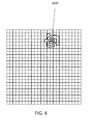
- FIG. 4 illustrates an exemplary contour plot that represents the space the brutal force approach has to search when there are two parameters of the design rules.
- the horizontal and vertical axes represent the values of the two parameters of the design rules.
- the depth represents the metric, higher value of which is more favorable.
- the brutal force approach has to calculate at each grid the optimal values of the parameters of the lithographic projection apparatus, before eventually finding the favorable value of the metric in the grid 1000 marked in FIG. 4 .
- step 405 parameters (interchangeably referred to as “design variables”) of the pattern transfer process are obtained.
- step 410 parameters (interchangeably referred to as “design variables”) of design rules are obtained.
- step 415 simultaneously optimizing the design variables of the pattern transfer process and the parameters of design rules.
- the optimization in step 415 is conducted to derive values of the design variables that yield the favorable value of the metric.
- the optimization in step 415 may include consecutively optimizing both the design variables of the pattern transfer process and the design variables of design rules.
- the results of the optimization, including values of the design variables of the pattern transfer process and values of the parameters of the design rules are output in step 420 .
- the optimization can be performed using a cost function, which may be expressed as follows
- w p is a weight constant assigned to f p (z 1 , z 2 , . . . , z N ).
- Examples of the evaluation points can be any physical point or pattern on the wafer, or any point on a virtual design layout, or resist image, or aerial image. Since it is the resist image that often dictates the circuit pattern on a substrate, f p (z 1 , z 2 , . . . , z N ) often includes a representation of the resist image. For example, f p (z 1 , z 2 , . . . , z N ) of such an evaluation point can be simply a distance between a point in the resist image to an intended position of that point (i.e., edge placement error EPE p (z 1 , z 2 , . . . , z N )).
- the design variables of the pattern transfer process can be any adjustable parameters such as adjustable parameters of the source, the reticle, the projection optics, dose, focus, etc. In an embodiment, at least some of the design variables are adjustable characteristics of the projection optics.
- the projection optics may include components collectively called a “wavefront manipulator” that can be used to adjust shapes of a wavefront and intensity distribution and/or phase shift of the irradiation beam.
- the projection optics can adjust a wavefront and intensity distribution at any location along an optical path of the lithographic projection apparatus, such as before the reticle, near a pupil plane, near an image plane, near a focal plane.
- the projection optics can be used to correct or compensate for certain distortions of the wavefront and intensity distribution caused by, for example, the source, the reticle, temperature variation in the lithographic projection apparatus, thermal expansion of components of the lithographic projection apparatus. Adjusting the wavefront and intensity distribution can change values of f p (z 1 , z 2 , . . . , z N ) and the cost function. Such changes can be simulated from a model or actually measured.
- the weighted RMS of f p (z 1 , z 2 , . . . , z N ) and Eq. 1 may be utilized interchangeably for notational simplicity herein.
- the cost function may include f p (z 1 , z 2 , . . . , z N ) under different PW conditions. For example, if N PW conditions are considered, the cost functions can be written as
- n 1, . . . , N.
- EPE edge placement errors
- minimizing the above cost function in Eq. 1′ is equivalent to minimizing the edge shift under various PW conditions, thus this leads to maximizing the PW.
- minimizing the above cost function also includes the minimization of MEEF (Mask Error Enhancement Factor), which is defined as the ratio between the wafer EPE and the induced mask edge bias.
- the design variables may have constraints, which can be expressed as (z 1 , z 2 , . . . , z N ) ⁇ Z, where Z is a set of possible values of the design variables.
- the constraints may represent physical restrictions in a hardware implementation of the lithographic projection apparatus.
- the constraints may include but not limited to one or more of: tuning ranges, interdependence between the design variables.
- step 415 therefore is to find a set of values of the design variables, under the constraints (z 1 , z 2 , . . . , z N ) ⁇ Z, if any, that minimize the cost function, i.e., to find
- cost function may have other suitable forms such as
- the cost function can be minimized (or maximized for a cost function of certain form, such as
- step 415 An exemplary optimization process of step 415 is further illustrated in FIG. 6 .
- This optimization process comprises a step 505 of defining a multi-variable cost function of a plurality of design variables (z 1 , z 2 , . . . , z N ).
- (z 1 , z 2 , . . . , z N ) include at least some design variable of the pattern transfer process and some design variables of the design rules.
- the design variables (z 1 , z 2 , . . . , z N ) may include characteristics of the illumination source and the reticle design layout.
- the cost function is calculated from the design variables.
- the aerial image or the resist image may be calculated. This is done using the models depicted in FIG. 2 .
- the optimization process proceeds to step 515 where it is determined if a particular or predetermined termination condition is satisfied.
- the predetermined termination condition may be any suitable condition, such as the cost function reaching a minimum or a maximum, the cost function being equal to a threshold value or having crossed the threshold value, the cost function having reached within a preset error limit, or a preset number of iteration or a predefined computation time being reached. If the termination condition in step 515 is satisfied, the optimization process ends. If the termination condition in step 515 is not satisfied, the optimization process proceeds to step 520 where values of the design variables are changed, and then back to step 510 to reevaluate the cost function using the changed values of the design variables.
- Procedures 510 - 520 are iteratively repeated until the termination condition is satisfied.
- the design variables of the pattern transfer process and the design variables of the design rules can be optimized simultaneously (referred to as simultaneous optimization), according to an embodiment, or can be optimized successively.
- simultaneous optimization the terms “simultaneous”, “simultaneously”, “joint” and “jointly” as used herein mean that the design variables of the pattern transfer process and the design variables of the design rules and/or any other design variables, are allowed to change at the same time.
- FIG. 7 is an exemplary block diagram that illustrates a computer system 100 which can assist in embodying and/or implementing the pattern selection method disclosed herein.
- Computer system 100 includes a bus 102 or other communication mechanism for communicating information, and one or more processor(s) 104 (and 105 ) coupled with bus 102 for processing information.
- Computer system 100 also includes a main memory 106 , such as a random access memory (RAM) or other dynamic storage device, coupled to bus 102 for storing information and instructions to be executed by processor 104 .
- Main memory 106 also may be used for storing temporary variables or other intermediate information during execution of instructions to be executed by processor 104 .
- Computer system 100 further includes a read only memory (ROM) 108 or other static storage device coupled to bus 102 for storing static information and instructions for processor 104 .
- ROM read only memory
- a storage device 110 such as a magnetic disk or optical disk, is provided and coupled to bus 102 for storing information and instructions.
- Computer system 100 may be coupled via bus 102 to a display 112 , such as a cathode ray tube (CRT) or flat panel or touch panel display for displaying information to a computer user.
- a display 112 such as a cathode ray tube (CRT) or flat panel or touch panel display for displaying information to a computer user.
- An input device 114 is coupled to bus 102 for communicating information and command selections to processor 104 .
- cursor control 116 is Another type of user input device, such as a mouse, a trackball, or cursor direction keys for communicating direction information and command selections to processor 104 and for controlling cursor movement on display 112 .
- This input device typically has two degrees of freedom in two axes, a first axis (e.g., x) and a second axis (e.g., y), that allows the device to specify positions in a plane.
- a touch panel (screen) display may also be used as an input device.
- portions of the simulation process may be performed by computer system 100 in response to processor 104 executing one or more sequences of one or more instructions contained in main memory 106 .
- Such instructions may be read into main memory 106 from another computer-readable medium, such as storage device 110 .
- Execution of the sequences of instructions contained in main memory 106 causes processor 104 to perform the process steps described herein.
- processors in a multi-processing arrangement may also be employed to execute the sequences of instructions contained in main memory 106 .
- hard-wired circuitry may be used in place of or in combination with software instructions. Thus, embodiments are not limited to any specific combination of hardware circuitry and software.
- Non-volatile media include, for example, optical or magnetic disks, such as storage device 110 .
- Volatile media include dynamic memory, such as main memory 106 .
- Transmission media include coaxial cables, copper wire and fiber optics, including the wires that comprise bus 102 . Transmission media can also take the form of acoustic or light waves, such as those generated during radio frequency (RF) and infrared (IR) data communications.
- RF radio frequency
- IR infrared
- Computer-readable media include, for example, a floppy disk, a flexible disk, hard disk, magnetic tape, any other magnetic medium, a CD-ROM, DVD, any other optical medium, punch cards, paper tape, any other physical medium with patterns of holes, a RAM, a PROM, and EPROM, a FLASH-EPROM, any other memory chip or cartridge, a carrier wave as described hereinafter, or any other medium from which a computer can read.
- Various forms of computer readable media may be involved in carrying one or more sequences of one or more instructions to processor 104 for execution.
- the instructions may initially be borne on a magnetic disk of a remote computer.
- the remote computer can load the instructions into its dynamic memory and send the instructions over a telephone line using a modem.
- a modem local to computer system 100 can receive the data on the telephone line and use an infrared transmitter to convert the data to an infrared signal.
- An infrared detector coupled to bus 102 can receive the data carried in the infrared signal and place the data on bus 102 .
- Bus 102 carries the data to main memory 106 , from which processor 104 retrieves and executes the instructions.
- the instructions received by main memory 106 may optionally be stored on storage device 110 either before or after execution by processor 104 .
- Computer system 100 also preferably includes a communication interface 118 coupled to bus 102 .
- Communication interface 118 provides a two-way data communication coupling to a network link 120 that is connected to a local network 122 .
- communication interface 118 may be an integrated services digital network (ISDN) card or a modem to provide a data communication connection to a corresponding type of telephone line.
- ISDN integrated services digital network
- communication interface 118 may be a local area network (LAN) card to provide a data communication connection to a compatible LAN.
- LAN local area network
- Wireless links may also be implemented.
- communication interface 118 sends and receives electrical, electromagnetic or optical signals that carry digital data streams representing various types of information.
- Network link 120 typically provides data communication through one or more networks to other data devices.
- network link 120 may provide a connection through local network 122 to a host computer 124 or to data equipment operated by an Internet Service Provider (ISP) 126 .
- ISP 126 in turn provides data communication services through the worldwide packet data communication network, now commonly referred to as the “Internet” 128 .
- Internet 128 uses electrical, electromagnetic or optical signals that carry digital data streams.
- the signals through the various networks and the signals on network link 120 and through communication interface 118 , which carry the digital data to and from computer system 100 are exemplary forms of carrier waves transporting the information.
- Computer system 100 can send messages and receive data, including program code, through the network(s), network link 120 , and communication interface 118 .
- a server 130 might transmit a requested code for an application program through Internet 128 , ISP 126 , local network 122 and communication interface 118 .
- one such downloaded application provides for the test pattern selection of the embodiment, for example.
- the received code may be executed by processor 104 as it is received, and/or stored in storage device 110 , or other non-volatile storage for later execution. In this manner, computer system 100 may obtain application code in the form of a carrier wave.
- FIG. 8 schematically depicts an exemplary lithographic projection apparatus whose performance could be simulated and/or optimized utilizing the methods described herein.
- the apparatus comprises:
- the apparatus is of a transmissive type (i.e., has a transmissive mask). However, in general, it may also be of a reflective type, for example (with a reflective mask). Alternatively, the apparatus may employ another kind of patterning means as an alternative to the use of a mask; examples include a programmable mirror array or LCD matrix.
- the source SO (e.g., a mercury lamp or excimer laser) produces a beam of radiation.
- This beam is fed into an illumination system (illuminator) IL, either directly or after having traversed conditioning means, such as a beam expander or beam delivery system BD, for example.
- the illuminator IL may comprise adjusting means AD for setting the outer and/or inner radial extent (commonly referred to as -outer and -inner, respectively) of the intensity distribution in the beam.
- it will generally comprise various other components, such as an integrator IN and a condenser CO. In this way, the beam B impinging on the mask MA has a desired uniformity and intensity distribution in its cross section.
- the source SO may be within the housing of the lithographic projection apparatus (as is often the case when the source SO is a mercury lamp, for example), but that it may also be remote from the lithographic projection apparatus, the radiation beam that it produces being led into the apparatus (e.g., with the aid of suitable directing minors); this latter scenario is often the case when the source SO is an excimer laser (e.g., based on KrF, ArF or F2 lasing).
- the current invention encompasses at least both of these scenarios.
- the beam B subsequently intercepts the mask MA, which is held on a mask table MT. Having traversed the mask MA, the beam B passes through the lens PS, which focuses the beam PS onto a target portion C of the substrate W. With the aid of the second positioning means (and interferometric measuring means IF), the substrate table WT can be moved accurately, e.g. so as to position different target portions C in the path of the beam B. Similarly, the first positioning means can be used to accurately position the mask MA with respect to the path of the beam B, e.g., after mechanical retrieval of the mask MA from a mask library, or during a scan.
- the object tables MT, WT will be realized with the aid of a long-stroke module (coarse positioning) and a short-stroke module (fine positioning), which are not explicitly depicted in FIG. 8 .
- the mask table MT may just be connected to a short stroke actuator, or may be fixed.
- Patterning device MA and substrate W may be aligned using alignment marks M 1 , M 2 in the patterning device, and alignment marks P 1 , P 2 on the wafer, as required.
- the depicted tool can be used in two different modes:
- the concepts disclosed herein may simulate or mathematically model any generic imaging system for imaging sub wavelength features, and may be especially useful with emerging imaging technologies capable of producing wavelengths of an increasingly smaller size.
- Emerging technologies already in use include DUV (deep ultra violet) lithography that is capable of producing a 193 nm wavelength with the use of a ArF laser, and even a 157 nm wavelength with the use of a Fluorine laser.
- EUV lithography is capable of producing wavelengths within a range of 20-5 nm by using a synchrotron or by hitting a material (either solid or a plasma) with high energy electrons in order to produce photons within this range.
- illumination may be produced by reflective minors with a multi-stack of Molybdenum and Silicon.
- the multi-stack minor has a 40 layer pairs of Molybdenum and Silicon where the thickness of each layer is a quarter wavelength. Even smaller wavelengths may be produced with X-ray lithography.
- a synchrotron is used to produce an X-ray wavelength. Since most material is absorptive at x-ray wavelengths, a thin piece of absorbing material defines where features would print (positive resist) or not print (negative resist).
- EUV extreme ultra violet
- EUV lithography is capable of producing wavelengths within a range of 20-5 nm by using a synchrotron or by hitting a material (either solid or a plasma) with high energy electrons in order to produce photons within this range.
Landscapes
- Engineering & Computer Science (AREA)
- Physics & Mathematics (AREA)
- General Physics & Mathematics (AREA)
- Computer Hardware Design (AREA)
- Theoretical Computer Science (AREA)
- Evolutionary Computation (AREA)
- Geometry (AREA)
- General Engineering & Computer Science (AREA)
- Exposure And Positioning Against Photoresist Photosensitive Materials (AREA)
Abstract
Description
wherein (z1, z2, . . . , zN) are N design variables or values thereof; (z1, z2, . . . , zN) include at least some design variable of the pattern transfer process and some design variables of the design rules; fp(z1, z2, . . . , zN) is a metric characteristic of the pattern transfer process, such as a difference between an actual value and an intended value of a characteristic at the p-th evaluation point for a set of values of the design variables of (z1, z2, . . . , zN), focus, CD, image shift, image distortion, image rotation, edge placement error, resist contour distance, critical dimension uniformity, dose variation, focus variation, process condition variation, mask error (MEEF), mask complexity defect size, and focus shift, etc. wp is a weight constant assigned to fp(z1, z2, . . . , zN). Examples of the evaluation points can be any physical point or pattern on the wafer, or any point on a virtual design layout, or resist image, or aerial image. Since it is the resist image that often dictates the circuit pattern on a substrate, fp(z1, z2, . . . , zN) often includes a representation of the resist image. For example, fp(z1, z2, . . . , zN) of such an evaluation point can be simply a distance between a point in the resist image to an intended position of that point (i.e., edge placement error EPEp(z1, z2, . . . , zN)). The design variables of the pattern transfer process can be any adjustable parameters such as adjustable parameters of the source, the reticle, the projection optics, dose, focus, etc. In an embodiment, at least some of the design variables are adjustable characteristics of the projection optics. The projection optics may include components collectively called a “wavefront manipulator” that can be used to adjust shapes of a wavefront and intensity distribution and/or phase shift of the irradiation beam. The projection optics can adjust a wavefront and intensity distribution at any location along an optical path of the lithographic projection apparatus, such as before the reticle, near a pupil plane, near an image plane, near a focal plane. The projection optics can be used to correct or compensate for certain distortions of the wavefront and intensity distribution caused by, for example, the source, the reticle, temperature variation in the lithographic projection apparatus, thermal expansion of components of the lithographic projection apparatus. Adjusting the wavefront and intensity distribution can change values of fp(z1, z2, . . . , zN) and the cost function. Such changes can be simulated from a model or actually measured.
therefore, minimizing the weighted RMS of fp(z1, z2, . . . , zN) is equivalent to minimizing the cost function
defined in Eq. 1. Thus the weighted RMS of fp(z1, z2, . . . , zN) and Eq. 1 may be utilized interchangeably for notational simplicity herein.
where fp
or a combination thereof.
using any suitable method such as the Gauss-Newton algorithm, the interpolation method, the Levenberg-Marquardt algorithm, the gradient descent algorithm, simulated annealing, the interior point method, the genetic algorithm, solving polynomials.
-
- a radiation system Ex, IL, for supplying a projection beam B of radiation. In this particular case, the radiation system also comprises a radiation source SO;
- a first object table (mask table) MT provided with a mask holder for holding a mask MA (e.g., a reticle), and connected to first positioning means PM for accurately positioning the mask with respect to projection system PS;
- a second object table (substrate table) WT provided with a substrate holder for holding a substrate W (e.g., a resist coated silicon wafer), and connected to second positioning means PW for accurately positioning the substrate with respect to projection system PS;
- a projection system (“lens”) PS (e.g., a refractive, catoptric or catadioptric optical system) for imaging an irradiated portion of the mask MA onto a target portion C (e.g., comprising one or more dies) of the substrate W.
-
- In step mode, the mask table MT is kept essentially stationary, and an entire mask image is projected in one go (i.e., a single “flash”) onto a target portion C. The substrate table WT is then shifted in the x and/or y directions so that a different target portion C can be irradiated by the beam B;
- In scan mode, essentially the same scenario applies, except that a given target portion C is not exposed in a single “flash”. Instead, the mask table MT is movable in a given direction (the so called “scan direction”, e.g., the y direction) with a speed v, so that the projection beam PB is caused to scan over a mask image; concurrently, the substrate table WT is simultaneously moved in the same or opposite direction at a speed V=Mv, in which M is the magnification of the lens PL (typically, M=¼ or ⅕). In this manner, a relatively large target portion C can be exposed, without having to compromise on resolution.
- 1. A method for obtaining values of one or more design variables of one or more design rules for a pattern transfer process comprising a lithographic projection apparatus, the method comprising:
- 2. The method of
clause 1, wherein the optimizing comprises deriving values of the one or more design variables of the pattern transfer process and the one or more design variables of the one or more design rules that yield a favorable value of a metric characteristic of the pattern transfer process. - 3. The method of
clause 1, wherein the optimizing comprises evaluating a cost function that measures a metric characteristic of the pattern transfer process, the cost function being a function of one or more design variables of the pattern transfer process and one or more design variables of the one or more design rules. - 4. The method of any one of clauses 2-3, wherein the metric characteristic of the pattern transfer process is a process window of the pattern transfer process.
- 5. The method of any one of clauses 1-4, wherein the one or more design variables of the pattern transfer process are selected from a group consisting of parameters of the lithographic projection apparatus and parameters of pre-exposure or post-exposure procedures.
- 6. The method of any one of clauses 1-4, wherein the one or more design variables of the one or more design rules comprise one or more constraints on parameters of patterns configured for being imaged via the pattern transfer process.
- 7. The method of clause 6, wherein the parameters of patterns comprise geometric parameters of the patterns.
- 8. The method of clause 6, wherein the parameters of the patterns are selected from a group consisting of an edge-to-edge distance between two patterns, a height of a pattern, a width of a pattern, an absolute position of an edge of a pattern, a distance between an edge of a pattern to an extended line of another edge of the same pattern or of a different pattern, a corner-to-corner distance, a dimension of an overlap between two patterns, a distance between an edge of a pattern to a fixed point on the one or more reticles, an aspect ratio of a pattern, and pitches of an array of patterns.
- 9. The method of clause 6, wherein the patterns are configured for being imaged via different layers in the pattern transfer process.
- 10. The method of any one of clauses 1-9, wherein both the lithographic projection apparatus and the one or more design rules affect the pattern transfer process.
- 11. The method of clauses 2-3, wherein the optimizing comprises changing one or more values of the one or more design variables of the pattern transfer process and the one or more design variables of the one or more design rules, until a termination condition is satisfied.
- 12. The method of clauses 11, further comprising reevaluating the cost function.
- 13. The method of any one of clauses 11-12, wherein the termination condition includes one or more of: minimization of the cost function; maximization of the cost function; reaching a preset number of iterations; reaching a value of the cost function equal to or beyond a preset threshold value; reaching a predefined computation time; reaching a preset number iteration, and reaching a value of the cost function within a preset error limit.
- 14. The method of
clause 13, wherein the cost function is minimized or maximized by a method selected from a group consisting of the Gauss-Newton algorithm, the interpolation method, the Levenberg-Marquardt algorithm, the gradient descent algorithm, simulated annealing, interior point method, and the genetic algorithm. - 15. The method of
clause 1, wherein the optimizing is performed under constraints of at least one of the one or more design variables of the pattern transfer process and the one or more design variables of the one or more design rules. - 16. The method of any one of clauses 3, 12-15, wherein the cost function is a function of one or more of focus, CD, image shift, image distortion, image rotation, edge placement error, resist contour distance, critical dimension uniformity, dose variation, focus variation, process condition variation, mask error (MEEF), mask complexity defect size, and focus shift.
- 17. The method of clause 5, wherein the pre-exposure or post-exposure procedures comprise one or more of pre-exposure or post-exposure baking (e.g., temperature and duration), post-exposure etching (e.g., etchant composition, etching duration), resist coating, and resist development.
- 18. The method of clause 5, wherein the parameters of the lithographic projection apparatus comprise parameters of one or more of dose, mask bias, projection optics and illumination source shape.
- 19. A computer program product comprising a computer readable medium having instructions recorded thereon, the instructions when executed by a computer implementing the method of any of the above clauses.
Claims (21)
Priority Applications (1)
| Application Number | Priority Date | Filing Date | Title |
|---|---|---|---|
| US14/398,416 US9489479B2 (en) | 2012-05-04 | 2013-04-16 | Rule and lithographic process co-optimization |
Applications Claiming Priority (3)
| Application Number | Priority Date | Filing Date | Title |
|---|---|---|---|
| US201261642765P | 2012-05-04 | 2012-05-04 | |
| PCT/EP2013/057938 WO2013164187A1 (en) | 2012-05-04 | 2013-04-16 | Design rule and lithographic process co-optimization |
| US14/398,416 US9489479B2 (en) | 2012-05-04 | 2013-04-16 | Rule and lithographic process co-optimization |
Publications (2)
| Publication Number | Publication Date |
|---|---|
| US20150089459A1 US20150089459A1 (en) | 2015-03-26 |
| US9489479B2 true US9489479B2 (en) | 2016-11-08 |
Family
ID=48190489
Family Applications (1)
| Application Number | Title | Priority Date | Filing Date |
|---|---|---|---|
| US14/398,416 Active 2033-04-30 US9489479B2 (en) | 2012-05-04 | 2013-04-16 | Rule and lithographic process co-optimization |
Country Status (4)
| Country | Link |
|---|---|
| US (1) | US9489479B2 (en) |
| NL (1) | NL2010647A (en) |
| TW (1) | TWI474104B (en) |
| WO (1) | WO2013164187A1 (en) |
Cited By (6)
| Publication number | Priority date | Publication date | Assignee | Title |
|---|---|---|---|---|
| US20160165462A1 (en) * | 2014-12-09 | 2016-06-09 | Futurewei Technologies, Inc. | Self-Learning, Adaptive Approach for Intelligent Analytics-Assisted Self-Organizing-Networks (SONs) |
| US20160239601A1 (en) * | 2015-02-18 | 2016-08-18 | Kabushiki Kaisha Toshiba | Mask data generation system, mask data generation method, and recording medium |
| US10083272B2 (en) * | 2016-08-12 | 2018-09-25 | International Business Machines Corporation | Integrated circuit design layout optimizer based on process variation and failure mechanism |
| US10191366B2 (en) | 2014-06-25 | 2019-01-29 | Asml Netherlands B.V. | Etch variation tolerant optimization |
| US10327159B2 (en) | 2014-12-09 | 2019-06-18 | Futurewei Technologies, Inc. | Autonomous, closed-loop and adaptive simulated annealing based machine learning approach for intelligent analytics-assisted self-organizing-networks (SONs) |
| US10592627B2 (en) | 2017-09-25 | 2020-03-17 | International Business Machines Corporation | Optimizing integrated circuit designs based on interactions between multiple integration design rules |
Families Citing this family (21)
| Publication number | Priority date | Publication date | Assignee | Title |
|---|---|---|---|---|
| US9613175B2 (en) | 2014-01-28 | 2017-04-04 | Globalfoundries Inc. | Method, computer system and computer-readable storage medium for creating a layout of an integrated circuit |
| US20150246476A1 (en) * | 2014-03-02 | 2015-09-03 | Seagate Technology Llc | Method for fabricating rectangular pattered stacks |
| KR20160131110A (en) * | 2014-03-18 | 2016-11-15 | 에이에스엠엘 네델란즈 비.브이. | Pattern placement error aware optimization |
| WO2017080729A1 (en) * | 2015-11-13 | 2017-05-18 | Asml Netherlands B.V. | Methods for identifying a process window boundary |
| WO2017162471A1 (en) * | 2016-03-24 | 2017-09-28 | Asml Netherlands B.V. | Optimization of a lithographic projection apparatus accounting for an interlayer characteristic |
| US9870612B2 (en) * | 2016-06-06 | 2018-01-16 | Taiwan Semiconductor Manufacturing Co., Ltd. | Method for repairing a mask |
| KR102450492B1 (en) * | 2016-10-21 | 2022-09-30 | 에이에스엠엘 네델란즈 비.브이. | How to determine the correction for the patterning process |
| US10915031B1 (en) * | 2017-02-07 | 2021-02-09 | Synopsys, Inc. | Optical source compensation |
| CN109254494B (en) * | 2017-07-12 | 2021-11-12 | 中芯国际集成电路制造(上海)有限公司 | Optical proximity correction method |
| US10635776B1 (en) * | 2017-07-14 | 2020-04-28 | Synopsys, Inc. | Producing mask layouts with rounded corners |
| CN107463309B (en) * | 2017-08-21 | 2020-12-25 | 郑州航空工业管理学院 | Entropy maximization criterion interactive evolution optimization method for wallpaper design |
| US10394116B2 (en) | 2017-09-06 | 2019-08-27 | International Business Machines Corporation | Semiconductor fabrication design rule loophole checking for design for manufacturability optimization |
| WO2019121486A1 (en) | 2017-12-22 | 2019-06-27 | Asml Netherlands B.V. | Process window based on defect probability |
| US10621295B2 (en) | 2018-04-10 | 2020-04-14 | International Business Machines Corporation | Incorporation of process variation contours in design rule and risk estimation aspects of design for manufacturability to increase fabrication yield |
| WO2020135946A1 (en) | 2018-12-28 | 2020-07-02 | Asml Netherlands B.V. | Method for generating patterning device pattern at patch boundary |
| CN111399334B (en) * | 2019-01-03 | 2021-12-21 | 无锡华润上华科技有限公司 | Mask manufacturing method and mask |
| US11182929B2 (en) * | 2019-02-25 | 2021-11-23 | Center For Deep Learning In Electronics Manufacturing, Inc. | Methods and systems for compressing shape data for electronic designs |
| US10877367B2 (en) * | 2019-08-30 | 2020-12-29 | Intel Corporation | Adaptive algorithm to generate optical proximity correction lithographic recipe |
| JP2023045120A (en) | 2021-09-21 | 2023-04-03 | キオクシア株式会社 | Mask design method and recording medium for the same |
| CN116934668B (en) * | 2022-04-11 | 2025-08-15 | 中芯国际集成电路制造(上海)有限公司 | Forming method and system of temperature compensation distribution diagram and temperature compensation method |
| CN120722645B (en) * | 2025-08-28 | 2025-11-21 | 全芯智造技术有限公司 | Calibration methods, electronic devices, and storage media for optical proximity correction models |
Citations (19)
| Publication number | Priority date | Publication date | Assignee | Title |
|---|---|---|---|---|
| US7194704B2 (en) | 2003-12-17 | 2007-03-20 | Kabushiki Kaisha Toshiba | Design layout preparing method |
| US7587704B2 (en) | 2005-09-09 | 2009-09-08 | Brion Technologies, Inc. | System and method for mask verification using an individual mask error model |
| US20090296055A1 (en) * | 2008-06-03 | 2009-12-03 | Jun Ye | Lens heating compensation systems and methods |
| US20110099526A1 (en) * | 2009-10-28 | 2011-04-28 | Asml Netherlands B.V. | Pattern Selection for Full-Chip Source and Mask Optimization |
| US20110230999A1 (en) * | 2008-11-21 | 2011-09-22 | Luoqi Chen | Fast Freeform Source and Mask Co-Optimization Method |
| US8136078B2 (en) | 2007-10-26 | 2012-03-13 | Imec | Optimization |
| US20120117521A1 (en) * | 2010-11-10 | 2012-05-10 | Asml Netherlands B.V. | Pattern-Dependent Proximity Matching/Tuning Including Light Manipulation By Projection Optics |
| US20120117522A1 (en) * | 2010-11-10 | 2012-05-10 | Asml Netherlands B.V. | Optimization of Source, Mask and Projection Optics |
| US20120124529A1 (en) * | 2010-11-17 | 2012-05-17 | Asml Netherlands B.V. | Pattern-Independent and Hybrid Matching/Tuning Including Light Manipulation by Projection Optics |
| US20120198396A1 (en) * | 2011-01-31 | 2012-08-02 | Masanari Kajiwara | Method of optimizing semiconductor device manufacturing process, method of manufacturing semiconductor device, and non-transitory computer readable medium |
| US20120227015A1 (en) | 2011-03-02 | 2012-09-06 | Texas Instruments Incorporated | Perturbational technique for co-optimizing design rules and illumination conditions for lithography process |
| US8336003B2 (en) * | 2010-02-19 | 2012-12-18 | International Business Machines Corporation | Method for designing optical lithography masks for directed self-assembly |
| US8415077B2 (en) * | 2010-08-13 | 2013-04-09 | International Business Machines Corporation | Simultaneous optical proximity correction and decomposition for double exposure lithography |
| US20130179847A1 (en) * | 2012-01-10 | 2013-07-11 | Asml Netherlands B.V. | Source Mask Optimization to Reduce Stochastic Effects |
| US20130212543A1 (en) * | 2012-02-09 | 2013-08-15 | Asml Netherlands B.V. | Lens heating aware source mask optimization for advanced lithography |
| US20130326437A1 (en) * | 2012-05-31 | 2013-12-05 | Asml Netherlands B.V. | Gradient-based pattern and evaluation point selection |
| US20140123082A1 (en) * | 2012-10-31 | 2014-05-01 | Asml Netherlands B.V. | Compensation for patterning device deformation |
| US8819601B2 (en) * | 2011-04-04 | 2014-08-26 | Asml Netherlands B.V. | Integration of lithography apparatus and mask optimization process with multiple patterning process |
| US8938696B1 (en) * | 2010-07-08 | 2015-01-20 | D2S, Inc. | Techniques of optical proximity correction using GPU |
Family Cites Families (3)
| Publication number | Priority date | Publication date | Assignee | Title |
|---|---|---|---|---|
| WO1997033205A1 (en) | 1996-03-06 | 1997-09-12 | Philips Electronics N.V. | Differential interferometer system and lithographic step-and-scan apparatus provided with such a system |
| US7491359B2 (en) * | 2003-10-16 | 2009-02-17 | Graham Packaging Pet Technologies Inc. | Delamination-resistant multilayer container, preform, article and method of manufacture |
| NL2005804A (en) * | 2010-01-14 | 2011-07-18 | Asml Netherlands Bv | Method and apparatus for enhancing signal strength for improved generation and placement of model-based sub-resolution assist features (mb-sraf). |
-
2013
- 2013-04-16 NL NL2010647A patent/NL2010647A/en not_active Application Discontinuation
- 2013-04-16 US US14/398,416 patent/US9489479B2/en active Active
- 2013-04-16 WO PCT/EP2013/057938 patent/WO2013164187A1/en not_active Ceased
- 2013-04-29 TW TW102115302A patent/TWI474104B/en active
Patent Citations (37)
| Publication number | Priority date | Publication date | Assignee | Title |
|---|---|---|---|---|
| US7194704B2 (en) | 2003-12-17 | 2007-03-20 | Kabushiki Kaisha Toshiba | Design layout preparing method |
| US7587704B2 (en) | 2005-09-09 | 2009-09-08 | Brion Technologies, Inc. | System and method for mask verification using an individual mask error model |
| US8136078B2 (en) | 2007-10-26 | 2012-03-13 | Imec | Optimization |
| US20090296055A1 (en) * | 2008-06-03 | 2009-12-03 | Jun Ye | Lens heating compensation systems and methods |
| US20140068530A1 (en) * | 2008-11-21 | 2014-03-06 | Asml Netherlands B.V. | Fast freeform source and mask co-optimization method |
| US8584056B2 (en) * | 2008-11-21 | 2013-11-12 | Asml Netherlands B.V. | Fast freeform source and mask co-optimization method |
| US20110230999A1 (en) * | 2008-11-21 | 2011-09-22 | Luoqi Chen | Fast Freeform Source and Mask Co-Optimization Method |
| US20110099526A1 (en) * | 2009-10-28 | 2011-04-28 | Asml Netherlands B.V. | Pattern Selection for Full-Chip Source and Mask Optimization |
| US20130311958A1 (en) * | 2009-10-28 | 2013-11-21 | Asml Netherlands B.V. | Pattern selection for full-chip source and mask optimization |
| US8739082B2 (en) * | 2009-10-28 | 2014-05-27 | Hua-yu Liu | Method of pattern selection for source and mask optimization |
| US20120216156A1 (en) * | 2009-10-28 | 2012-08-23 | Asml Netherlands B.V. | Method of Pattern Selection for Source and Mask Optimization |
| US9183324B2 (en) * | 2009-10-28 | 2015-11-10 | Asml Netherlands B.V. | Pattern selection for full-chip source and mask optimization |
| US8438508B2 (en) | 2009-10-28 | 2013-05-07 | Asml Netherlands B.V. | Pattern selection for full-chip source and mask optimization |
| US8336003B2 (en) * | 2010-02-19 | 2012-12-18 | International Business Machines Corporation | Method for designing optical lithography masks for directed self-assembly |
| US8856693B2 (en) * | 2010-02-19 | 2014-10-07 | International Business Machines Corporation | Method for designing optical lithography masks for directed self-assembly |
| US8938696B1 (en) * | 2010-07-08 | 2015-01-20 | D2S, Inc. | Techniques of optical proximity correction using GPU |
| US8415077B2 (en) * | 2010-08-13 | 2013-04-09 | International Business Machines Corporation | Simultaneous optical proximity correction and decomposition for double exposure lithography |
| US8560978B2 (en) * | 2010-11-10 | 2013-10-15 | Asml Netherlands B.V. | Pattern-dependent proximity matching/tuning including light manipulation by projection optics |
| US8893060B2 (en) * | 2010-11-10 | 2014-11-18 | Asml Netherlands B.V. | Optimization of source, mask and projection optics |
| US20140033145A1 (en) * | 2010-11-10 | 2014-01-30 | Asml Netherlands B.V. | Pattern-dependent proximity matching/tuning including light manipulation by projection optics |
| US20120117522A1 (en) * | 2010-11-10 | 2012-05-10 | Asml Netherlands B.V. | Optimization of Source, Mask and Projection Optics |
| US20150074622A1 (en) * | 2010-11-10 | 2015-03-12 | Asml Netherlands B.V. | Optimization of source, mask and projection optics |
| US20120117521A1 (en) * | 2010-11-10 | 2012-05-10 | Asml Netherlands B.V. | Pattern-Dependent Proximity Matching/Tuning Including Light Manipulation By Projection Optics |
| US8806394B2 (en) * | 2010-11-10 | 2014-08-12 | Asml Netherlands B.V. | Pattern-dependent proximity matching/tuning including light manipulation by projection optics |
| US20140282303A1 (en) * | 2010-11-17 | 2014-09-18 | Asml Netherlands B.V. | Pattern-independent and hybrid matching/tuning including light manipulation by projection optics |
| US20120124529A1 (en) * | 2010-11-17 | 2012-05-17 | Asml Netherlands B.V. | Pattern-Independent and Hybrid Matching/Tuning Including Light Manipulation by Projection Optics |
| US8745551B2 (en) * | 2010-11-17 | 2014-06-03 | Asml Netherlands B.V. | Pattern-independent and hybrid matching/tuning including light manipulation by projection optics |
| US20120198396A1 (en) * | 2011-01-31 | 2012-08-02 | Masanari Kajiwara | Method of optimizing semiconductor device manufacturing process, method of manufacturing semiconductor device, and non-transitory computer readable medium |
| US20120227015A1 (en) | 2011-03-02 | 2012-09-06 | Texas Instruments Incorporated | Perturbational technique for co-optimizing design rules and illumination conditions for lithography process |
| US8819601B2 (en) * | 2011-04-04 | 2014-08-26 | Asml Netherlands B.V. | Integration of lithography apparatus and mask optimization process with multiple patterning process |
| US20140365983A1 (en) * | 2011-04-04 | 2014-12-11 | Asml Netherlands B.V. | Integration of lithography apparatus and mask optimization process with multiple patterning process |
| US20130179847A1 (en) * | 2012-01-10 | 2013-07-11 | Asml Netherlands B.V. | Source Mask Optimization to Reduce Stochastic Effects |
| US9213783B2 (en) * | 2012-01-10 | 2015-12-15 | Asml Netherlands B.V. | Source mask optimization to reduce stochastic effects |
| US20130212543A1 (en) * | 2012-02-09 | 2013-08-15 | Asml Netherlands B.V. | Lens heating aware source mask optimization for advanced lithography |
| US20130326437A1 (en) * | 2012-05-31 | 2013-12-05 | Asml Netherlands B.V. | Gradient-based pattern and evaluation point selection |
| US8898599B2 (en) * | 2012-05-31 | 2014-11-25 | Asml Netherlands B.V. | Gradient-based pattern and evaluation point selection |
| US20140123082A1 (en) * | 2012-10-31 | 2014-05-01 | Asml Netherlands B.V. | Compensation for patterning device deformation |
Non-Patent Citations (2)
| Title |
|---|
| J. W. Blatchford et al., "Litho/Design Co-Optimization and Area Scaling for the 22-NM Logic Node" The Electrochemical Society pp. 449-454 (2010) (6 pages). |
| T. Dam et al., "Exploring the Impact of Mask Making Constraints on Double Patterning Design Rules", Proc. of SPIE vol. 8166 816629-1, (2011) (12 pages). |
Cited By (10)
| Publication number | Priority date | Publication date | Assignee | Title |
|---|---|---|---|---|
| US10191366B2 (en) | 2014-06-25 | 2019-01-29 | Asml Netherlands B.V. | Etch variation tolerant optimization |
| US10712653B2 (en) | 2014-06-25 | 2020-07-14 | Asml Netherlands B.V. | Etch variation tolerant optimization |
| US20160165462A1 (en) * | 2014-12-09 | 2016-06-09 | Futurewei Technologies, Inc. | Self-Learning, Adaptive Approach for Intelligent Analytics-Assisted Self-Organizing-Networks (SONs) |
| US10327159B2 (en) | 2014-12-09 | 2019-06-18 | Futurewei Technologies, Inc. | Autonomous, closed-loop and adaptive simulated annealing based machine learning approach for intelligent analytics-assisted self-organizing-networks (SONs) |
| US10382979B2 (en) * | 2014-12-09 | 2019-08-13 | Futurewei Technologies, Inc. | Self-learning, adaptive approach for intelligent analytics-assisted self-organizing-networks (SONs) |
| US20160239601A1 (en) * | 2015-02-18 | 2016-08-18 | Kabushiki Kaisha Toshiba | Mask data generation system, mask data generation method, and recording medium |
| US9858379B2 (en) * | 2015-02-18 | 2018-01-02 | Toshiba Memory Corporation | Mask data generation system, mask data generation method, and recording medium |
| US10083272B2 (en) * | 2016-08-12 | 2018-09-25 | International Business Machines Corporation | Integrated circuit design layout optimizer based on process variation and failure mechanism |
| US10592627B2 (en) | 2017-09-25 | 2020-03-17 | International Business Machines Corporation | Optimizing integrated circuit designs based on interactions between multiple integration design rules |
| US10628544B2 (en) | 2017-09-25 | 2020-04-21 | International Business Machines Corporation | Optimizing integrated circuit designs based on interactions between multiple integration design rules |
Also Published As
| Publication number | Publication date |
|---|---|
| US20150089459A1 (en) | 2015-03-26 |
| NL2010647A (en) | 2013-11-06 |
| TW201403215A (en) | 2014-01-16 |
| WO2013164187A1 (en) | 2013-11-07 |
| TWI474104B (en) | 2015-02-21 |
Similar Documents
| Publication | Publication Date | Title |
|---|---|---|
| US9489479B2 (en) | Rule and lithographic process co-optimization | |
| US12554203B2 (en) | Model for calculating a stochastic variation in an arbitrary pattern | |
| US10955755B2 (en) | Optimization of assist features and source | |
| US10401732B2 (en) | Optimization flows of source, mask and projection optics | |
| US20220179321A1 (en) | Method for determining pattern in a patterning process | |
| US9235662B2 (en) | Lithography model for 3D resist profile simulations | |
| US9619607B2 (en) | Method and apparatus for cost function based simultaneous OPC and SBAR optimization | |
| US10712653B2 (en) | Etch variation tolerant optimization | |
| US8819601B2 (en) | Integration of lithography apparatus and mask optimization process with multiple patterning process | |
| US10386727B2 (en) | Pattern placement error aware optimization | |
| US10331039B2 (en) | Rule-based deployment of assist features | |
| US8918744B2 (en) | Substrate-topography-aware lithography modeling | |
| US9835955B2 (en) | Lithography model for 3D topographic wafers | |
| US10796063B2 (en) | Mapping of patterns between design layout and patterning device | |
| US20230333483A1 (en) | Optimization of scanner throughput and imaging quality for a patterning process |
Legal Events
| Date | Code | Title | Description |
|---|---|---|---|
| AS | Assignment |
Owner name: ASML NETHERLANDS B.V., NETHERLANDS Free format text: ASSIGNMENT OF ASSIGNORS INTEREST;ASSIGNOR:LIU, XIAOFENG;REEL/FRAME:034125/0001 Effective date: 20120521 |
|
| STCF | Information on status: patent grant |
Free format text: PATENTED CASE |
|
| FEPP | Fee payment procedure |
Free format text: PAYOR NUMBER ASSIGNED (ORIGINAL EVENT CODE: ASPN); ENTITY STATUS OF PATENT OWNER: LARGE ENTITY |
|
| CC | Certificate of correction | ||
| MAFP | Maintenance fee payment |
Free format text: PAYMENT OF MAINTENANCE FEE, 4TH YEAR, LARGE ENTITY (ORIGINAL EVENT CODE: M1551); ENTITY STATUS OF PATENT OWNER: LARGE ENTITY Year of fee payment: 4 |
|
| MAFP | Maintenance fee payment |
Free format text: PAYMENT OF MAINTENANCE FEE, 8TH YEAR, LARGE ENTITY (ORIGINAL EVENT CODE: M1552); ENTITY STATUS OF PATENT OWNER: LARGE ENTITY Year of fee payment: 8 |